spice-user's guide and reference
TRANSCRIPT

i
SPICE:
User’s Guide and Reference
August 20, 2002
Michael B. Steer and Paul D. Franzon
ii
Copyright c© 1993 by FIMAC, Inc., Michael B. Steer and Paul D. Franzon. Michael Steerand Paul Franzon can be contacted at Department of Electrical and Computer Engineering,North Carolina State University, Raleigh, North Carolina U.S.A. NC 27695 (fax +1-919-515-5523).
All rights reserved. Printed in the United States of America. Except as permitted under theUnited States Copyright Act of 1976, no part of this publication may be reproduced, storedin a data base or retrieval system or transmitted, in any form or by any means, electronic,mechanical, photocopying, recording or otherwise without the written permission withoutthe permission of the publisher.
Spice2g6 is a trademark of U.C. Berkeley.Spice3 is a trademark of U.C. Berkeley.PSpice probe, parts, device equations and digital files are trademarks of Microsim Corp.All other trademarks are the properties of their respective owners.
This document was prepared using LATEX.Diagrams were prepared using idraw and gnuplot.
Information contained in this work is believed to be reliable and obtained from sources that are also believed to be
reliable. However, neither FIMAC, Inc., nor its authors guarantees the completeness or accuracy of any information
contained herein and neither FIMAC, Inc. nor its authors shall be reesonsible for any errors, omissions, or damages
arising out of use of this information. This work is published with the understanding that FIMAC, Inc. and its
authors are supplying information but are not attempting to render engineering or other professional services. If
such services are required, the assistance of an appropriate professional should be sought.
Contents
PART I SPICE BASICS 1
1 Introduction 11.1 Introduction . . . . . . . . . . . . . . . . . . . . . . . . . . . . . . . . . . . . . 11.2 How to use this book . . . . . . . . . . . . . . . . . . . . . . . . . . . . . . . . 21.3 What Spice Does . . . . . . . . . . . . . . . . . . . . . . . . . . . . . . . . . 21.4 justspice versions . . . . . . . . . . . . . . . . . . . . . . . . . . . . . . . . . . 31.5 How to Get Spice . . . . . . . . . . . . . . . . . . . . . . . . . . . . . . . . . 31.6 Documentation Conventions . . . . . . . . . . . . . . . . . . . . . . . . . . . . 5
2 Getting Started 72.1 The Input File . . . . . . . . . . . . . . . . . . . . . . . . . . . . . . . . . . . 72.2 Running Spice and Viewing the Output . . . . . . . . . . . . . . . . . . . . . 102.3 Error Messages . . . . . . . . . . . . . . . . . . . . . . . . . . . . . . . . . . . 13
3 Carrying On 153.1 Elements . . . . . . . . . . . . . . . . . . . . . . . . . . . . . . . . . . . . . . 15
3.1.1 Inductors and Mutual Inductors . . . . . . . . . . . . . . . . . . . . . 153.1.2 Active Devices . . . . . . . . . . . . . . . . . . . . . . . . . . . . . . . 163.1.3 Transmission Lines . . . . . . . . . . . . . . . . . . . . . . . . . . . . . 183.1.4 Voltage and Current Sources . . . . . . . . . . . . . . . . . . . . . . . 20
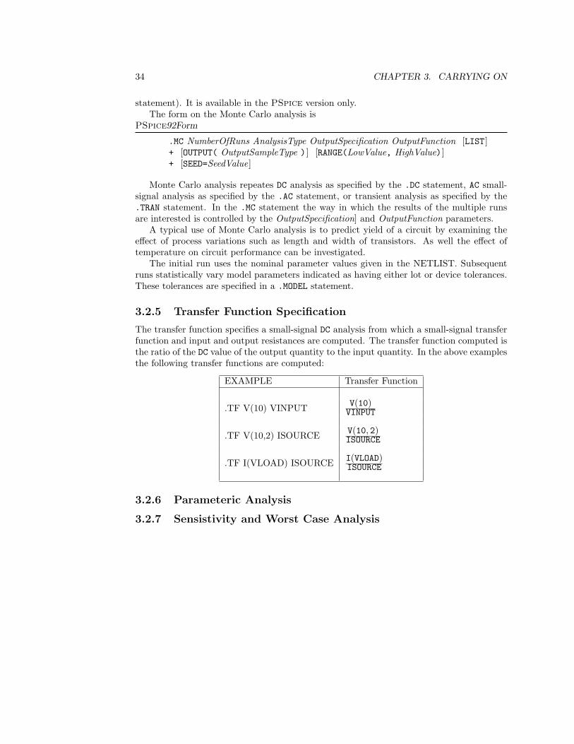
3.2 Analyses . . . . . . . . . . . . . . . . . . . . . . . . . . . . . . . . . . . . . . . 243.2.1 Transient Analysis . . . . . . . . . . . . . . . . . . . . . . . . . . . . . 243.2.2 DC Analyses . . . . . . . . . . . . . . . . . . . . . . . . . . . . . . . . 293.2.3 Small Signal AC Analysis . . . . . . . . . . . . . . . . . . . . . . . . . 323.2.4 Monte Carlo Analysis . . . . . . . . . . . . . . . . . . . . . . . . . . . 333.2.5 Transfer Function Specification . . . . . . . . . . . . . . . . . . . . . . 343.2.6 Parameteric Analysis . . . . . . . . . . . . . . . . . . . . . . . . . . . . 343.2.7 Sensistivity and Worst Case Analysis . . . . . . . . . . . . . . . . . . . 34
4 How Spice Works 434.1 Introduction . . . . . . . . . . . . . . . . . . . . . . . . . . . . . . . . . . . . . 434.2 AC Small Signal Analysis . . . . . . . . . . . . . . . . . . . . . . . . . . . . . 444.3 DC Analysis . . . . . . . . . . . . . . . . . . . . . . . . . . . . . . . . . . . . 45
iii
iv CONTENTS
4.4 Discussion . . . . . . . . . . . . . . . . . . . . . . . . . . . . . . . . . . . . . . 454.5 To Explore Further . . . . . . . . . . . . . . . . . . . . . . . . . . . . . . . . . 46
PART II SPICE SYNTAX 47
5 Input File 475.1 Introduction . . . . . . . . . . . . . . . . . . . . . . . . . . . . . . . . . . . . . 475.2 Circuit Model . . . . . . . . . . . . . . . . . . . . . . . . . . . . . . . . . . . . 475.3 Input Lines . . . . . . . . . . . . . . . . . . . . . . . . . . . . . . . . . . . . . 49
5.3.1 Analysis Statements . . . . . . . . . . . . . . . . . . . . . . . . . . . . 505.3.2 Control Statements . . . . . . . . . . . . . . . . . . . . . . . . . . . . . 515.3.3 Elements . . . . . . . . . . . . . . . . . . . . . . . . . . . . . . . . . . 535.3.4 Distributed Elements . . . . . . . . . . . . . . . . . . . . . . . . . . . . 545.3.5 Source Elements . . . . . . . . . . . . . . . . . . . . . . . . . . . . . . 545.3.6 Interface Elements . . . . . . . . . . . . . . . . . . . . . . . . . . . . . 55
5.4 Input Grammar . . . . . . . . . . . . . . . . . . . . . . . . . . . . . . . . . . . 555.4.1 Prefixes and Units . . . . . . . . . . . . . . . . . . . . . . . . . . . . . 56
5.5 Parameters . . . . . . . . . . . . . . . . . . . . . . . . . . . . . . . . . . . . . 565.6 Expressions . . . . . . . . . . . . . . . . . . . . . . . . . . . . . . . . . . . . . 58
5.6.1 Polynomials . . . . . . . . . . . . . . . . . . . . . . . . . . . . . . . . 595.6.2 Laplace Expressions . . . . . . . . . . . . . . . . . . . . . . . . . . . . 615.6.3 Chebyschev . . . . . . . . . . . . . . . . . . . . . . . . . . . . . . . . 61
5.7 Function Definition .FUNC PSpice92 Only . . . . . . . . . . . . . . . . . . 615.8 Limits . . . . . . . . . . . . . . . . . . . . . . . . . . . . . . . . . . . . . . . . 635.9 Syntax Variations . . . . . . . . . . . . . . . . . . . . . . . . . . . . . . . . . . 63
PART III CATALOG 64
6 Statement Catalog 65.AC, AC Analysis . . . . . . . . . . . . . . . . . . . . . . . . . . . . . . . . . . . . . 67COMMENT, Comment Card . . . . . . . . . . . . . . . . . . . . . . . . . . . . . . 69.DC, DC Analysis . . . . . . . . . . . . . . . . . . . . . . . . . . . . . . . . . . . . 70.DISTO, Spice2g6 (?) and Spice3 Only: Small-Signal Distortion Analysis . . . . 74.DISTRIBUTION, PSpice Only: Distribution Specification . . . . . . . . . . . . . 77.END, End Statement . . . . . . . . . . . . . . . . . . . . . . . . . . . . . . . . . . 79.ENDS, End Subcircuit Statement . . . . . . . . . . . . . . . . . . . . . . . . . . . 80.FOUR, Fourier Analysis . . . . . . . . . . . . . . . . . . . . . . . . . . . . . . . . . 81.FUNC, PSpice92 Only: Function Definition . . . . . . . . . . . . . . . . . . . . . 82.IC, Initial Conditions . . . . . . . . . . . . . . . . . . . . . . . . . . . . . . . . . . 83.INC, PSpice Only: Include Statement . . . . . . . . . . . . . . . . . . . . . . . . 84.LIB, PSpice Only: Library Statement . . . . . . . . . . . . . . . . . . . . . . . . 85.MC, PSpice Only: Monte Carlo Analysis . . . . . . . . . . . . . . . . . . . . . . . 87.MODEL, Model Statement . . . . . . . . . . . . . . . . . . . . . . . . . . . . . . . 90
CONTENTS v
.NODESET, Node Voltage Initialization . . . . . . . . . . . . . . . . . . . . . . . . 95
.NOISE, Small-Signal Noise Analysis . . . . . . . . . . . . . . . . . . . . . . . . . . 96
.OP, Operating Point Analysis . . . . . . . . . . . . . . . . . . . . . . . . . . . . . 99
.OPTIONS, Option Specification . . . . . . . . . . . . . . . . . . . . . . . . . . . . 100
.PARAM, PSpice92 Only: Parameter Definition . . . . . . . . . . . . . . . . . . . 106
.PLOT, Plot Specification . . . . . . . . . . . . . . . . . . . . . . . . . . . . . . . . 108
.PRINT, Print Specification . . . . . . . . . . . . . . . . . . . . . . . . . . . . . . . 113
.PROBE, PSpice Only: Data Output Specification . . . . . . . . . . . . . . . . . . 121
.PZ, Spice3Only: Pole-Zero Analysis . . . . . . . . . . . . . . . . . . . . . . . . . . 123
.SAVEBIAS, PSpice92 Only : Save Bias Conditions . . . . . . . . . . . . . . . . . 125
.SENS, PSpice Only: Sensitivity Analysis . . . . . . . . . . . . . . . . . . . . . . . 126
.STEP, PSpice92 Only: Parameteric Analysis . . . . . . . . . . . . . . . . . . . . 127
.SUBCKT, Subcircuit Statement . . . . . . . . . . . . . . . . . . . . . . . . . . . . 128
.TEMP, Temperature Specification . . . . . . . . . . . . . . . . . . . . . . . . . . . 131
.TEXT, PSpice92 Only: Text Parameter Definition . . . . . . . . . . . . . . . . . 132
.TF, PSpice Only: Transfer Function Specification . . . . . . . . . . . . . . . . . . 133TITLE, Title Line . . . . . . . . . . . . . . . . . . . . . . . . . . . . . . . . . . . . 134.TRAN, Transient Analysis . . . . . . . . . . . . . . . . . . . . . . . . . . . . . . . 135.WATCH, PSpice92 Only: Watch Analysis Statement . . . . . . . . . . . . . . . . 137.WCASE, PSpice92 Only: Sensitivity and Worst Case Analysis . . . . . . . . . . 138.WIDTH, Width Specification . . . . . . . . . . . . . . . . . . . . . . . . . . . . . . 141
7 Element Catalog 143B, GaAs MESFET . . . . . . . . . . . . . . . . . . . . . . . . . . . . . . . . . . . . 145C, Capacitor . . . . . . . . . . . . . . . . . . . . . . . . . . . . . . . . . . . . . . . 182D, Diode . . . . . . . . . . . . . . . . . . . . . . . . . . . . . . . . . . . . . . . . . 186E, Voltage-Controlled Voltage Source . . . . . . . . . . . . . . . . . . . . . . . . . . 191F, Current-Controlled Current Source . . . . . . . . . . . . . . . . . . . . . . . . . 195G, Voltage-Controlled Current Source . . . . . . . . . . . . . . . . . . . . . . . . . 197H, Current-Controlled Voltage Source . . . . . . . . . . . . . . . . . . . . . . . . . 201I, Independent Current Source . . . . . . . . . . . . . . . . . . . . . . . . . . . . . 203J, Junction Field-Effect Transistor . . . . . . . . . . . . . . . . . . . . . . . . . . . 212K, Mutual Inductor . . . . . . . . . . . . . . . . . . . . . . . . . . . . . . . . . . . 221L, Inductor . . . . . . . . . . . . . . . . . . . . . . . . . . . . . . . . . . . . . . . . 229M, MOSFET . . . . . . . . . . . . . . . . . . . . . . . . . . . . . . . . . . . . . . . 231N, PSpiceonly: Digital Input Interface . . . . . . . . . . . . . . . . . . . . . . . . 266O, PSpiceonly: Digital Output Interface . . . . . . . . . . . . . . . . . . . . . . . 270Q, Bipolar Junction Transistor . . . . . . . . . . . . . . . . . . . . . . . . . . . . . 273R, Resistor . . . . . . . . . . . . . . . . . . . . . . . . . . . . . . . . . . . . . . . . 283S, Voltage Controlled Switch . . . . . . . . . . . . . . . . . . . . . . . . . . . . . . 286T, Transmission Line . . . . . . . . . . . . . . . . . . . . . . . . . . . . . . . . . . . 290U, PSpiceonly: Digital Device . . . . . . . . . . . . . . . . . . . . . . . . . . . . . 294U, Universal Element . . . . . . . . . . . . . . . . . . . . . . . . . . . . . . . . . . . 295V, Independent Voltage Source . . . . . . . . . . . . . . . . . . . . . . . . . . . . . 297
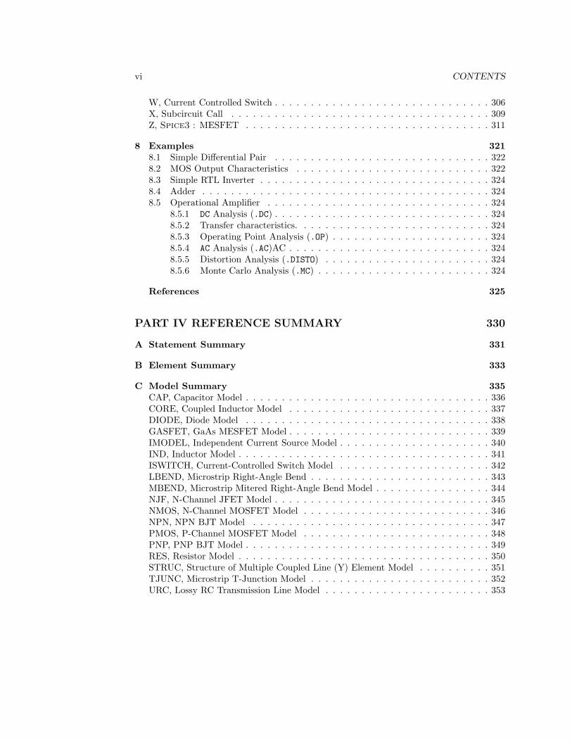
vi CONTENTS
W, Current Controlled Switch . . . . . . . . . . . . . . . . . . . . . . . . . . . . . . 306X, Subcircuit Call . . . . . . . . . . . . . . . . . . . . . . . . . . . . . . . . . . . . 309Z, Spice3 : MESFET . . . . . . . . . . . . . . . . . . . . . . . . . . . . . . . . . . 311
8 Examples 3218.1 Simple Differential Pair . . . . . . . . . . . . . . . . . . . . . . . . . . . . . . 3228.2 MOS Output Characteristics . . . . . . . . . . . . . . . . . . . . . . . . . . . 3228.3 Simple RTL Inverter . . . . . . . . . . . . . . . . . . . . . . . . . . . . . . . . 3248.4 Adder . . . . . . . . . . . . . . . . . . . . . . . . . . . . . . . . . . . . . . . . 3248.5 Operational Amplifier . . . . . . . . . . . . . . . . . . . . . . . . . . . . . . . 324
8.5.1 DC Analysis (.DC) . . . . . . . . . . . . . . . . . . . . . . . . . . . . . . 3248.5.2 Transfer characteristics. . . . . . . . . . . . . . . . . . . . . . . . . . . 3248.5.3 Operating Point Analysis (.OP) . . . . . . . . . . . . . . . . . . . . . . 3248.5.4 AC Analysis (.AC)AC . . . . . . . . . . . . . . . . . . . . . . . . . . . . 3248.5.5 Distortion Analysis (.DISTO) . . . . . . . . . . . . . . . . . . . . . . . 3248.5.6 Monte Carlo Analysis (.MC) . . . . . . . . . . . . . . . . . . . . . . . . 324
References 325
PART IV REFERENCE SUMMARY 330
A Statement Summary 331
B Element Summary 333
C Model Summary 335CAP, Capacitor Model . . . . . . . . . . . . . . . . . . . . . . . . . . . . . . . . . . 336CORE, Coupled Inductor Model . . . . . . . . . . . . . . . . . . . . . . . . . . . . 337DIODE, Diode Model . . . . . . . . . . . . . . . . . . . . . . . . . . . . . . . . . . 338GASFET, GaAs MESFET Model . . . . . . . . . . . . . . . . . . . . . . . . . . . . 339IMODEL, Independent Current Source Model . . . . . . . . . . . . . . . . . . . . . 340IND, Inductor Model . . . . . . . . . . . . . . . . . . . . . . . . . . . . . . . . . . . 341ISWITCH, Current-Controlled Switch Model . . . . . . . . . . . . . . . . . . . . . 342LBEND, Microstrip Right-Angle Bend . . . . . . . . . . . . . . . . . . . . . . . . . 343MBEND, Microstrip Mitered Right-Angle Bend Model . . . . . . . . . . . . . . . . 344NJF, N-Channel JFET Model . . . . . . . . . . . . . . . . . . . . . . . . . . . . . . 345NMOS, N-Channel MOSFET Model . . . . . . . . . . . . . . . . . . . . . . . . . . 346NPN, NPN BJT Model . . . . . . . . . . . . . . . . . . . . . . . . . . . . . . . . . 347PMOS, P-Channel MOSFET Model . . . . . . . . . . . . . . . . . . . . . . . . . . 348PNP, PNP BJT Model . . . . . . . . . . . . . . . . . . . . . . . . . . . . . . . . . . 349RES, Resistor Model . . . . . . . . . . . . . . . . . . . . . . . . . . . . . . . . . . . 350STRUC, Structure of Multiple Coupled Line (Y) Element Model . . . . . . . . . . 351TJUNC, Microstrip T-Junction Model . . . . . . . . . . . . . . . . . . . . . . . . . 352URC, Lossy RC Transmission Line Model . . . . . . . . . . . . . . . . . . . . . . . 353

CONTENTS vii
VMODEL, Independent Voltage Source . . . . . . . . . . . . . . . . . . . . . . . . 354VSWITCH, Voltage-Controlled Switch Model . . . . . . . . . . . . . . . . . . . . . 355XJUNC, Microstrip X-junction . . . . . . . . . . . . . . . . . . . . . . . . . . . . . 356ZSTEP, Microstrip Impedance Step Model . . . . . . . . . . . . . . . . . . . . . . . 357
D Summary of Expressions and Parameters 359D.1 Predefined Parameters . . . . . . . . . . . . . . . . . . . . . . . . . . . . . . . 359D.2 Algebraic Expressions . . . . . . . . . . . . . . . . . . . . . . . . . . . . . . . 360
E Error 361E.1 Introduction . . . . . . . . . . . . . . . . . . . . . . . . . . . . . . . . . . . . . 361E.2 List of Errors . . . . . . . . . . . . . . . . . . . . . . . . . . . . . . . . . . . . 362
F Reference Card 375

viii CONTENTS

List of Figures
2.1 Example circuit and corresponding input file. . . . . . . . . . . . . . . . . . . 82.2 Portions of the Spice output file. . . . . . . . . . . . . . . . . . . . . . . . . . 112.3 Example of output produced by the .plot control statement. . . . . . . . . . 122.4 Results plotted graphically. . . . . . . . . . . . . . . . . . . . . . . . . . . . . 13
3.1 TTL Circuit Description. . . . . . . . . . . . . . . . . . . . . . . . . . . . . . 173.2 Symbols used for a MOSFET and a top and side view of what a MOSFET
transistor looks like ‘in the silicon’. . . . . . . . . . . . . . . . . . . . . . . . . 193.3 Example of a MOSFET element specification. . . . . . . . . . . . . . . . . . . 203.4 A CMOS inverter. . . . . . . . . . . . . . . . . . . . . . . . . . . . . . . . . . 353.5 Example of a transmission line. . . . . . . . . . . . . . . . . . . . . . . . . . . 363.6 DC response example. Two alternative analyses are presented at the bottom
and are described in the text. . . . . . . . . . . . . . . . . . . . . . . . . . . . 373.7 Output V-I characteristics for CMOS inverter. . . . . . . . . . . . . . . . . . 383.8 LC filter and the Spice file specifying a frequency response analysis. (Com-
ments in emphasis are not part of the file.) . . . . . . . . . . . . . . . . . . . 393.9 Frequency response of the circuit shown in Figure 3.8. . . . . . . . . . . . . . 403.10 Output impedance vs. frequency for LC circuit shown in in Figure 3.8. . . . . 41
4.1 Definition of networks: (a) N ; and (b) N ′. . . . . . . . . . . . . . . . . . . . . 44
5.1 The Spice circuit representation. . . . . . . . . . . . . . . . . . . . . . . . . . 48
6.1 Two port definition for pole-zero analysis. . . . . . . . . . . . . . . . . . . . 1236.2 Subcircuit. . . . . . . . . . . . . . . . . . . . . . . . . . . . . . . . . . . . . . . 128
7.1 B — GASFET element. . . . . . . . . . . . . . . . . . . . . . . . . . . . . . . 1457.2 Schematic of the GASFET model . . . . . . . . . . . . . . . . . . . . . . . . . 1467.3 MESFET parasitic resistance parameter relationships. . . . . . . . . . . . . . 1557.4 GASFET leakage current parameter dependencies. . . . . . . . . . . . . . . . 1557.5 LEVEL 1 (Curtice model) I/V dependencies. . . . . . . . . . . . . . . . . . . 1577.6 LEVEL 1 (Curtice model) capacitance dependencies. . . . . . . . . . . . . . 1587.7 LEVEL 2 (Raytheon model) I/V dependencies. . . . . . . . . . . . . . . . . 159
ix

x LIST OF FIGURES
7.8 LEVEL 2 (Raytheon model) capacitance dependencies. . . . . . . . . . . . . 1607.9 LEVEL 3 (TOM model) I/V dependencies. . . . . . . . . . . . . . . . . . . . 1617.10 LEVEL 3 (TOM model) capacitance dependencies. . . . . . . . . . . . . . . 1637.11 LEVEL -1 (TOM-2 model) I/V dependencies. . . . . . . . . . . . . . . . . . 1647.12 LEVEL 3 (TOM model) I/V dependencies. . . . . . . . . . . . . . . . . . . . 1657.13 LEVEL 3 (TOM model) capacitance dependencies. . . . . . . . . . . . . . . 1677.14 LEVEL -1 (TOM-2 model) I/V dependencies. . . . . . . . . . . . . . . . . . 1687.15 LEVEL 4 (Curtice cubic model) I/V dependencies. . . . . . . . . . . . . . . 1697.16 LEVEL 4 (Curtice Cubic model) capacitance dependencies. . . . . . . . . . 1697.17 MESFET parasitic resistance parameter relationships. . . . . . . . . . . . . . 1737.18 LEVEL 5 (Materka-Kacprzak model) I/V dependencies. . . . . . . . . . . . 1747.19 LEVEL 5 (Materka-Kacprzak model) capacitance dependencies. . . . . . . . 1757.20 MESFET parasitic resistance parameter relationships. . . . . . . . . . . . . . 1777.21 LEVEL 6 (Angelov model) I/V dependencies. . . . . . . . . . . . . . . . . . 1787.22 LEVEL 6 (Angelov model) capacitance dependencies. . . . . . . . . . . . . . 1797.23 Small signal GASFET model . . . . . . . . . . . . . . . . . . . . . . . . . . . 1797.24 C — capacitor element. . . . . . . . . . . . . . . . . . . . . . . . . . . . . . . 1827.25 D — diode element. . . . . . . . . . . . . . . . . . . . . . . . . . . . . . . . . 1867.26 Schematic of diode element model. . . . . . . . . . . . . . . . . . . . . . . . . 1877.27 E — voltage-controlled voltage source element. . . . . . . . . . . . . . . . . . 1917.28 F — current-controlled current source element. . . . . . . . . . . . . . . . . . 1957.29 G — voltage-controlled current source element. . . . . . . . . . . . . . . . . . 1977.30 H — current-controlled voltage source element. . . . . . . . . . . . . . . . . . 2017.31 I — independent current source. . . . . . . . . . . . . . . . . . . . . . . . . . 2037.32 Current source exponential (EXP) waveform . . . . . . . . . . . . . . . . . . . 2077.33 Current source single frequency frequency modulation (SFFM) waveform . . . 2077.34 Current source transient pulse (PULSE) waveform . . . . . . . . . . . . . . . . 2097.35 Current source transient piece-wise linear (PWL) waveform . . . . . . . . . . . 2097.36 Current source transient sine (SIN) waveform . . . . . . . . . . . . . . . . . . 2117.37 J — Junction field effect transistor element . . . . . . . . . . . . . . . . . . . 2127.38 Schematic of the JFET model . . . . . . . . . . . . . . . . . . . . . . . . . . . 2147.39 JFET parasitic resistance parameter relationships. . . . . . . . . . . . . . . . 2177.40 JFET leakage current parameter dependecies. . . . . . . . . . . . . . . . . . 2177.41 I/V dependencies. . . . . . . . . . . . . . . . . . . . . . . . . . . . . . . . . . 2187.42 JFET capacitance dependencies. . . . . . . . . . . . . . . . . . . . . . . . . . 2197.43 K — Mutual inductor element. . . . . . . . . . . . . . . . . . . . . . . . . . . 2217.44 L — Inductor element. . . . . . . . . . . . . . . . . . . . . . . . . . . . . . . . 2297.45 M — MOSFET element . . . . . . . . . . . . . . . . . . . . . . . . . . . . . . 2317.46 Schematic of LEVEL 1, 2 and 3 MOSFET models . . . . . . . . . . . . . . . . 2367.47 MOSFET LEVEL 1, 2 and 3 parasitic resistance parameter relationships. . . . 2427.48 MOSFET leakage current parameter dependecies. . . . . . . . . . . . . . . . 2437.49 MOSFET LEVEL 1, 2 and 3 depletion capacitance parameter relationships . . 2457.50 LEVEL 1 I/V dependencies. . . . . . . . . . . . . . . . . . . . . . . . . . . . 2467.51 MOSFET LEVEL 1 overlap capacitance parameter relationships. . . . . . . . 247
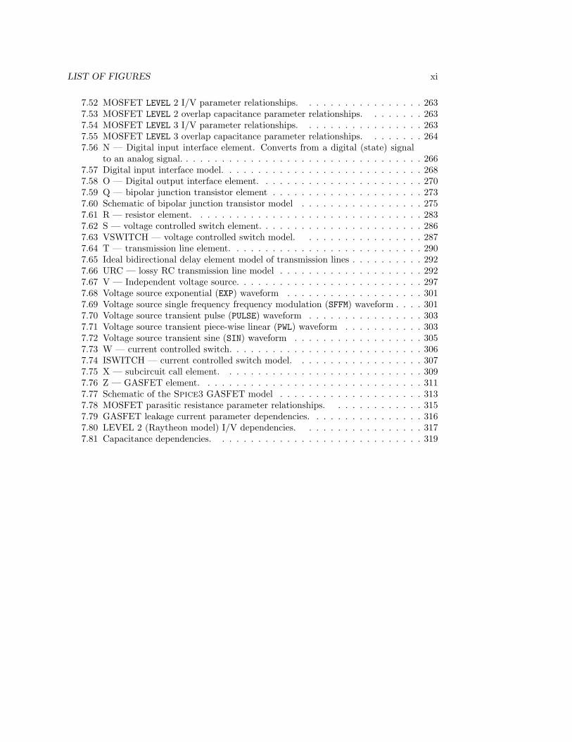
LIST OF FIGURES xi
7.52 MOSFET LEVEL 2 I/V parameter relationships. . . . . . . . . . . . . . . . . 2637.53 MOSFET LEVEL 2 overlap capacitance parameter relationships. . . . . . . . 2637.54 MOSFET LEVEL 3 I/V parameter relationships. . . . . . . . . . . . . . . . . 2637.55 MOSFET LEVEL 3 overlap capacitance parameter relationships. . . . . . . . 2647.56 N — Digital input interface element. Converts from a digital (state) signal
to an analog signal. . . . . . . . . . . . . . . . . . . . . . . . . . . . . . . . . . 2667.57 Digital input interface model. . . . . . . . . . . . . . . . . . . . . . . . . . . . 2687.58 O — Digital output interface element. . . . . . . . . . . . . . . . . . . . . . . 2707.59 Q — bipolar junction transistor element . . . . . . . . . . . . . . . . . . . . . 2737.60 Schematic of bipolar junction transistor model . . . . . . . . . . . . . . . . . 2757.61 R — resistor element. . . . . . . . . . . . . . . . . . . . . . . . . . . . . . . . 2837.62 S — voltage controlled switch element. . . . . . . . . . . . . . . . . . . . . . . 2867.63 VSWITCH — voltage controlled switch model. . . . . . . . . . . . . . . . . 2877.64 T — transmission line element. . . . . . . . . . . . . . . . . . . . . . . . . . . 2907.65 Ideal bidirectional delay element model of transmission lines . . . . . . . . . . 2927.66 URC — lossy RC transmission line model . . . . . . . . . . . . . . . . . . . . 2927.67 V — Independent voltage source. . . . . . . . . . . . . . . . . . . . . . . . . . 2977.68 Voltage source exponential (EXP) waveform . . . . . . . . . . . . . . . . . . . 3017.69 Voltage source single frequency frequency modulation (SFFM) waveform . . . . 3017.70 Voltage source transient pulse (PULSE) waveform . . . . . . . . . . . . . . . . 3037.71 Voltage source transient piece-wise linear (PWL) waveform . . . . . . . . . . . 3037.72 Voltage source transient sine (SIN) waveform . . . . . . . . . . . . . . . . . . 3057.73 W — current controlled switch. . . . . . . . . . . . . . . . . . . . . . . . . . . 3067.74 ISWITCH — current controlled switch model. . . . . . . . . . . . . . . . . . 3077.75 X — subcircuit call element. . . . . . . . . . . . . . . . . . . . . . . . . . . . 3097.76 Z — GASFET element. . . . . . . . . . . . . . . . . . . . . . . . . . . . . . . 3117.77 Schematic of the Spice3 GASFET model . . . . . . . . . . . . . . . . . . . . 3137.78 MOSFET parasitic resistance parameter relationships. . . . . . . . . . . . . 3157.79 GASFET leakage current parameter dependencies. . . . . . . . . . . . . . . . 3167.80 LEVEL 2 (Raytheon model) I/V dependencies. . . . . . . . . . . . . . . . . 3177.81 Capacitance dependencies. . . . . . . . . . . . . . . . . . . . . . . . . . . . . 319

xii LIST OF FIGURES
List of Tables
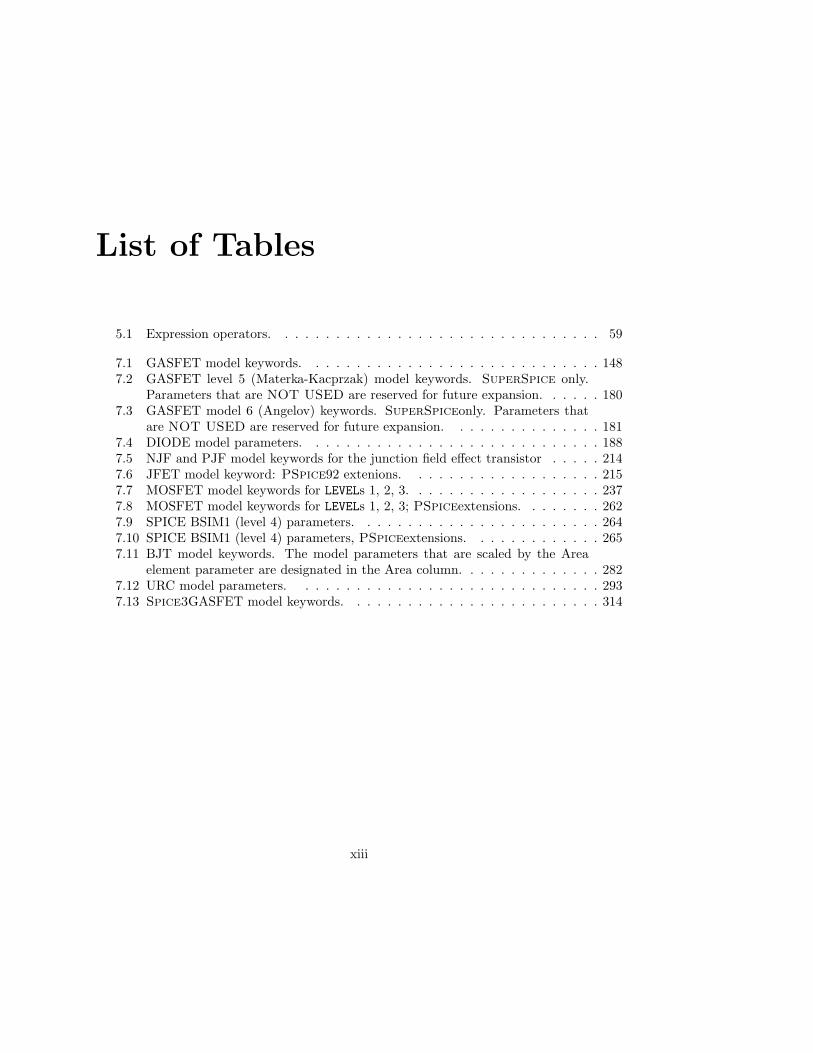
5.1 Expression operators. . . . . . . . . . . . . . . . . . . . . . . . . . . . . . . . 59
7.1 GASFET model keywords. . . . . . . . . . . . . . . . . . . . . . . . . . . . . 1487.2 GASFET level 5 (Materka-Kacprzak) model keywords. SuperSpice only.
Parameters that are NOT USED are reserved for future expansion. . . . . . 1807.3 GASFET model 6 (Angelov) keywords. SuperSpiceonly. Parameters that
are NOT USED are reserved for future expansion. . . . . . . . . . . . . . . 1817.4 DIODE model parameters. . . . . . . . . . . . . . . . . . . . . . . . . . . . . 1887.5 NJF and PJF model keywords for the junction field effect transistor . . . . . 2147.6 JFET model keyword: PSpice92 extenions. . . . . . . . . . . . . . . . . . . 2157.7 MOSFET model keywords for LEVELs 1, 2, 3. . . . . . . . . . . . . . . . . . . 2377.8 MOSFET model keywords for LEVELs 1, 2, 3; PSpiceextensions. . . . . . . . 2627.9 SPICE BSIM1 (level 4) parameters. . . . . . . . . . . . . . . . . . . . . . . . 2647.10 SPICE BSIM1 (level 4) parameters, PSpiceextensions. . . . . . . . . . . . . 2657.11 BJT model keywords. The model parameters that are scaled by the Area
element parameter are designated in the Area column. . . . . . . . . . . . . . 2827.12 URC model parameters. . . . . . . . . . . . . . . . . . . . . . . . . . . . . . 2937.13 Spice3GASFET model keywords. . . . . . . . . . . . . . . . . . . . . . . . . 314
xiii
xiv LIST OF TABLES
Preface
This book began because of a need for a better Spice manual for our students who useSpice3 in a multi workstation environment at the university and on their own IBM-PCcompatible computers. The great many low-cost Spicemanuals that are available are con-fined to just one commercial version of Spice (PSpiceby Microsim Corporation) and simplycause confusion when not used with PSpice. Many Spice users use several versions of Spiceand would like to know what the common denominator Spice syntax is. This book is a usersmanual and reference for three of the most commonly used Spice programs. Spice2g6isused as the common denominator of all Spice programs. PSpice and Spice3 extensionsof this “standard” are clearly identified. The book can be used as a reference by the userof any Spice-like program provided that the user restricts her or himself to the syntax ofSpice2g6. However personal computer versions of PSpice and Spice3 are available frombulletin boards (or by mail at low cost) although the Spice version is severely restricted asto the size of circuit which it can handle.
From the initial effort of developing a universal Spice manual, and with the feedbackfrom many Spice users in university and industry, the current manual was developed. Themanual has been written to support the needs of both novice and experienced users. Thefirst part of the book helps users get started with Spice perhaps for the first time. Then thealgorithms and methods that make Spice work are treated. The second part of the bookis a catalog of Spice statements and elements. The element catalog presents the electricalmodels of elements in a detail that has not been previously presented in a concise formbefore with a user perspective. An example is the clear explanation of the dependenciesof the parameters of the MOSFET models. A subject that can be particularly confusingotherwise. Most of the electrical models were developed by reverse engineering source codeas some have not been adequately documented previously. The reference section of themanual is well indexed and cross referenced making it easy to find desired information witha minimum number of indirections.
We continually strive to improve this manual and welcome your suggestions as to itsimprovement and your corrections.
Michael SteerNorth Carolina State Universityemail: [email protected]
Paul FranzonNorth Carolina State Universityemail: [email protected]
Chapter 1
Introduction
1.1 Introduction
Spice is a general-purpose circuit simulation program for nonlinear DC, nonlinear transient,and small-signal AC analyses. Circuits may contain resistors, capacitors, inductors, mutualinductors, independent voltage and current sources, dependent sources, transmission lines,switches, and the five most common semiconductor devices: diodes, BJTs, JFETs, MES-FETs, and MOSFETs. Spice was developed at the University of California at Berkeleyand after many years of effort culminated in the landmark Spice2g6 version. This wasthe last FORTRAN language version of Spice distributed by UC Berkeley and its syntaxand analysis options have become a standard for Spice-like simulators. With few excep-tions, all commercial versions and University versions of Spice are upwards compatiblewith Spice2g6 in that they support the complete syntax and analyses of Spice2g6. SinceSpice2g6 was released Spice3 was developed at UC Berkeley initially as a C languageequivalent of Spice2g6. The new capabilities of Spice3 include pole-zero analysis, andnew transistor models for MESFETs and for short and narrow channel MOSFETs as wellimproved numerical methods. Many commercial versions of Spice are based directly onSpice3. However there is a group of commercial Spice-like simulators that have signifi-cant advances over Spice2g6 and Spice3 in the areas of enhanced input syntax, improvedconvergence, better device models and more analysis types. Many of these enhanced Spiceprograms were completely rewritten and not ports of the Berkeley software. As can be ex-pected, the effort put into these commercial programs is reflected in their price. The firstSpice version for personal computers was the commerical program PSpice by MicroSimcorporation. PSpicenow has the largest customer base of all commerical Spice programs.Consequently the syntax of PSpice has become a second “standard”. The PSpice syntaxis upwards compatible to the Spice2g6 syntax. However, there are some incompatibilitiesbetween the Spice3 and PSpice syntaxes as PSpice was released before Spice3 becameavailable. The effect of this development is that all Spice simulators (including commer-cial programs) accept a Spice2g6 netlist but perhaps not a Spice3 netlist. Conflicts withSpice3 generally exist in the naming of additional elements and in the use of new models.
1
2 CHAPTER 1. INTRODUCTION
1.2 How to use this book
This manual is intended for both the novice and advanced user. If you are generally un-familiar with how to use Spice, or are not familiar with all of its features then Chapter 2and Chapter 3 are provided to get you started. The aim in Chapter 2 is just to help youwrite, run, and understand your first Spice file. In Chapter 3, each of the major typesof analyses Spice can do for you are introduced, by example. In contrast, Chapter ?? isintended for those wishing to understand how Spice works internally. Chapter 5 describesin the format of the Spice input file or netlist. Part II (Chapters 6 and 7) describe thesyntax of the Spice language and the predefined expressions provided within it. Part IIIsummarizes the Spice syntax, statements and elements in a quick look-up form suitable forthe experienced user. Chapter 9 presents more elaborate Spice examples. Also providedis a quick reference guide to Spice’s error messages and their meaning (Appendix E).
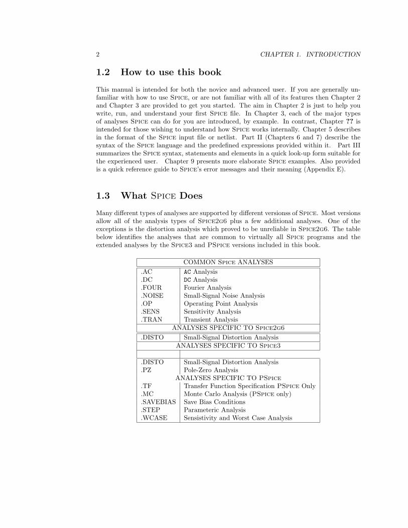
1.3 What Spice Does
Many different types of analyses are supported by different versionss of Spice. Most versionsallow all of the analysis types of Spice2g6 plus a few additional analyses. One of theexceptions is the distortion analysis which proved to be unreliable in Spice2g6. The tablebelow identifies the analyses that are common to virtually all Spice programs and theextended analyses by the Spice3 and PSpice versions included in this book.
COMMON Spice ANALYSES.AC AC Analysis.DC DC Analysis.FOUR Fourier Analysis.NOISE Small-Signal Noise Analysis.OP Operating Point Analysis.SENS Sensitivity Analysis.TRAN Transient Analysis
ANALYSES SPECIFIC TO Spice2g6
.DISTO Small-Signal Distortion AnalysisANALYSES SPECIFIC TO Spice3
.DISTO Small-Signal Distortion Analysis
.PZ Pole-Zero AnalysisANALYSES SPECIFIC TO PSpice
.TF Transfer Function Specification PSpice Only
.MC Monte Carlo Analysis (PSpice only)
.SAVEBIAS Save Bias Conditions
.STEP Parameteric Analysis
.WCASE Sensistivity and Worst Case Analysis
1.4. JUSTSPICE VERSIONS 3
1.4 justspice versions
This book is a manual for five versions of Spice: Spice2g6, Spice3, PSpice, Super-Spiceand HSpice. For these the input syntax, and models are described. Particularlyemphasis is given to Spice3 and PSpice as these are the most widley used Spice versions.For these the graphical user interface is also described.
The syntax, analysis types, and elements of Spice2g6form a common denominator withthe capabilities of Spice3and PSpicebeing extensions. Adhering to the Spice2g6 syntaxensures maximum portability of Spice netlists. Major restrictions of this syntax comparedto commercial versions include using integers to designate nodes. The Spice3syntax is justa small extension of the Spice2g6 syntax and is fully upwards compatible from Spice2g6.The PSpicesyntax is a considerable enhancement over the Spice2g6syntax. Highlights ofthe enhanced syntax are that node names are allowed which greatly increases the readibilityof the netlist, the use of symbolic expressions in place of numeric values, passing parametersto subcircuits, and many more analysis types. The PSpice syntax has become a second“standard” syntax.
Part II of this book serves as a combined user and reference manual while Part III isa condensed reference manual aimed at the experiendenced user needing to check syntax.Descriptions of statements and elements are based on the Spice2g6 syntax with the Spice3and PSpice extensions clearly identified.
1.5 How to Get Spice
PSpiceand Spice3 are the most widely used Spice-like programs. A student evaluationversion of PSpice for the PC is available on many bulletin boards. This program is full-functioned but the size of circuit with which it can be used is severely restricted. Anunrestricted PC version of Spice3 is also available on many bulletin boards and source codefrom which workstation versions can be made is available from the University of Californiaat Berkeley at nominal cost.
Spice3
The source code and makefiles for Spice3 is available from the Industrial Liason Office atthe University of California at Berkeley. The source code is possible to make a Spice3for virtually all workstations and similar computers. UC Berkeley allows for unlimitedredistribution of this code subject to their liabilty wnd export control conditions. The costfor the the Spice3 package was $250 at the time of writing. The office can be contactedusing
EECS/ERL Industrial Support Office497 Cory HallUniversity of CaliforniaBerkeley, CA 94720.
or by electronic mail using [email protected] . The ordering process is speeded upvia anonymous ftp of the liability waiver form and similar forms. The procedure is
4 CHAPTER 1. INTRODUCTION
¿ftp ilpsoft.berkeley.edulogin: anonymousEnter e-mail address as passwordpassword: your electronic mail address...ftp¿ cd pub ftp¿ get XXXX ...ftp¿ closeftp¿ quit¿
The file XXXX lists the files that are available and explains the procedure to follow.The make procedure for PC’s is not as straight forward for IBM-compatible personal
computers as for workstations. Fortunately a PC executable version of Spice3can be downloaded from various bulletin boards. Several bulletin boards that had this package are
wuarchive.wustl.eduoak.oakland.edu The executable is contained in
the file pub/msdos/electrical/spctr3e wich can be downloaded via anonlymous ftp (that this
by running ftp with the login anonymous). For example,
¿ftp your favorite bulletin board namelogin: anonymousEnter e-mail address as passwordpassword: your address.ftp> cd pub/msdos/electricalftp> get spctr3e.zipftp> closeftp> quit
A nominal fee is requested. Note that the pkunzip (sometimes called just unzip) programis required to unpack spctr3e using
pkunzip spctr3e.zipThe pkunzip program is almost certain to be available on the same bulletin board you usedto obtain spectr3e.
The disks for the PC version of Spice3are also available for a nominal fee by contactingX
Spice2g6
There is probably no good reason to use Spice2g6 rather than Spice3but here is how youcan get it anyway. Spice2g6 is also available by contacting the Industrial Liason Officeat the University of California using the same procedure as discussed above. Spice2g6 iswritten in FORTRAN while Spice3 is written in C.
A C version of Spice2g6 (automaticly converted from the FORTRAN by a FORTRAN-
1.6. DOCUMENTATION CONVENTIONS 5
to-C translator) is available via anonymous ftp from many bulletin boards including Xas the file pub/msdos/electrical/xxx. Follow the ftp procedure described above.
PSpice
An evaluation version of PSpice is available via anonymous ftp on the bulletin boards men-
tioned above. Three files are required:pspice5a.zippspice5b.zip andpspice5c.zip
The disks are also published by Prentice Hall as
PSpiceStudent Version Disks (—bf 2 5 1/4”disks) IBM PC compatible Release 5.0PSpiceStudent Version Disks (—bf 2 3 1/2”disks) IBM PS/2 compatible Release 5.0andPSpiceStudent Version Disks (2 3 1/2” disks)MAC II compatible Release 5.0
Microsim in the past has distributed these disks free to University and College instructors.The evaluation version of PSpice is full functioned but the size of circuit that can be sim-ulated is restricted. Microsim Corporation sells a professional version of PSpice for work-stations and minicomputers as well as the PC version. For information contact Microsimby calling 714-770-3022¿
1.6 Documentation Conventions
In this manual the general forms of statements and elements use the following conventionsto identify the type of input required:
1. Actual characters that must be typed by the user are in a typewriter font.
2. Input that must be replaced by a word or a numeric value is italicized.
3. Optional input is enclosed between square brackets “ [ ] ”.
4. Input that can be optionally repeated is followed by a string of dots “. . .”.
5. As in Spice input syntax a line is continued when a plus sign “+” appears in the firstcharacter position of the continued line.
As example the general form of resistor is
Rname N1 N2
+ ResistorValue IC=VR ]Here the first character on the first line is R which indicates that this line describes aresistor element. The full name of the resistor is Rname where name can be replaced by anyalphanumeric character string that uniquely identifies the element. Thus “R1”, “Rgate” and“ROP AMP 16 2” are names of resistors. It should be noted that Spice does not distinguish

6 CHAPTER 1. INTRODUCTION
between upper and lower case characters. ResistorValue must be replaced by the numericvalue of the resistor possibly including a scale factor. Thus 1MEG, 1E6, and 1000000. Thecomplete Spice input syntax is described in Chapter 5. With the exception of the linecontinuation indicated by the leading + sign a Spice element or statement must be fullycontained on a single line.
Chapter 2
Getting Started
In this chapter, we simulate a small circuit in order to introduce you to Spice. We describethe input file, or “circuit” file, showing you the generic structure of the file, and giving anumber of examples. Though in each example we describe what is shown, we do not list allthe options and variations for each item described. The reader is referred to the referencesections (chapters 6 and 7) for that. We then show you how to run Spice and discuss thedifferent features of the output file.
2.1 The Input File
A typical input file, and a schematic of the circuit and input waveform it is simulating, isshown in Figure 2.1. The input file is created with a text editor and is typically namedsomething like ‘test.cir’. The file is made up of five types of lines:
• A title line, up to 80 characters long, placed at the start of the file.
• An .end statement at the end of the file. This statement can be safely omitted inmany simulators but its usage is recommended for compatibility purposes.
• Any number of comment lines, each starting with ‘*’, can be placed anywhere afterthe title and before the end.
• Any number of element lines that describe the circuit to be simulated. The basicsyntax of the element line is
name node node ... value
where name is the name that you assign to the element. The first character in thename identifies the type of circuit element being described, e.g. ‘R’ for a resistor.From one to seven characters must then be added to the name to identify it uniquely,e.g. ‘R1’, or ‘Rpulldn’. Numbers are usually used. The node’s identify the nodesin the circuit to which the terminals or ‘leads’ of the circuit element are connected.
7

8 CHAPTER 2. GETTING STARTED
0
+
-V
in(t)
R1
C1
10k
100pF
1 2
V(2)
I(vin)
Simple RC Network Title Line** This is a comment Comments Lines*R1 1 2 500 Element LinesC1 2 0 5pvin 1 0 pulse (0 1.5 4ns 3ns 5ns 2ns 17ns)*.tran 500ps 34ns Control Statement Lines.print tran v(1) v(2) i(vin)*.end End Line
Figure 2.1: Example circuit and corresponding input file.
2.1. THE INPUT FILE 9
For example, one terminal of the capacitor ‘C1’ is connected to the node numbered‘0’, which must be used for the ground (or common reference) node, and the otherterminal is connected to node number ‘2’. In Spice each circuit node is identified bya unique number. value describes the value(s) needed to describe the element.
• Any number of control statement lines that specify what type of circuit analysis is tobe performed and how the results are to be reported.
The elements and control statement lines can be written in any order, even intermixed.
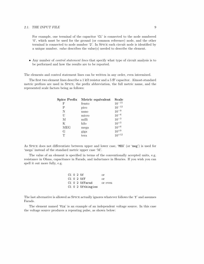
The first two element lines describe a 1 kΩ resistor and a 5 fF capacitor. Almost-standardmetric prefixes are used in Spice, the prefix abbreviation, the full metric name, and therepresented scale factors being as follows:
Spice Prefix Metric equivalent ScaleF femto 10−15
P pico 10−12
N nano 10−9
U micro 10−6
M milli 10−3
K kilo 10+3
MEG mega 10+6
G giga 10+9
T tera 10+12
As Spice does not differentiate between upper and lower case, ‘MEG’ (or ‘meg’) is used for‘mega’ instead of the standard metric upper case ‘M’.
The value of an element is specified in terms of the conventionally accepted units, e.g.resistance in Ohms, capacitance in Farads, and inductance in Henries. If you wish you canspell it out more fully, e.g.
C1 0 2 5f orC1 0 2 5fF orC1 0 2 5fFarad or evenC1 0 2 5fthingies
The last alternative is allowed as Spice actually ignores whatever follows the ‘f’ and assumesFarads.
The element named ‘Vin’ is an example of an independent voltage source. In this casethe voltage source produces a repeating pulse, as shown below:
10 CHAPTER 2. GETTING STARTED
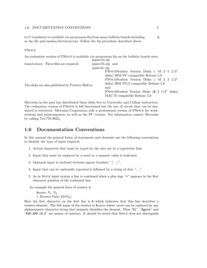
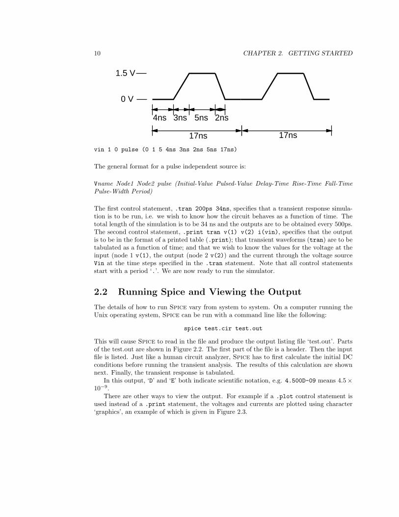
1.5 V
0 V
4ns 3ns 5ns 2ns
17ns 17ns
vin 1 0 pulse (0 1 5 4ns 3ns 2ns 5ns 17ns)
The general format for a pulse independent source is:
Vname Node1 Node2 pulse (Initial-Value Pulsed-Value Delay-Time Rise-Time Fall-TimePulse-Width Period)
The first control statement, .tran 200ps 34ns, specifies that a transient response simula-tion is to be run, i.e. we wish to know how the circuit behaves as a function of time. Thetotal length of the simulation is to be 34 ns and the outputs are to be obtained every 500ps.The second control statement, .print tran v(1) v(2) i(vin), specifies that the outputis to be in the format of a printed table (.print); that transient waveforms (tran) are to betabulated as a function of time; and that we wish to know the values for the voltage at theinput (node 1 v(1), the output (node 2 v(2)) and the current through the voltage sourceVin at the time steps specified in the .tran statement. Note that all control statementsstart with a period ‘.’. We are now ready to run the simulator.
2.2 Running Spice and Viewing the Output
The details of how to run Spice vary from system to system. On a computer running theUnix operating system, Spice can be run with a command line like the following:
spice test.cir test.out
This will cause Spice to read in the file and produce the output listing file ‘test.out’. Partsof the test.out are shown in Figure 2.2. The first part of the file is a header. Then the inputfile is listed. Just like a human circuit analyzer, Spice has to first calculate the initial DCconditions before running the transient analysis. The results of this calculation are shownnext. Finally, the transient response is tabulated.
In this output, ‘D’ and ‘E’ both indicate scientific notation, e.g. 4.500D-09 means 4.5×10⁻⁹.
There are other ways to view the output. For example if a .plot control statement isused instead of a .print statement, the voltages and currents are plotted using character‘graphics’, an example of which is given in Figure 2.3.
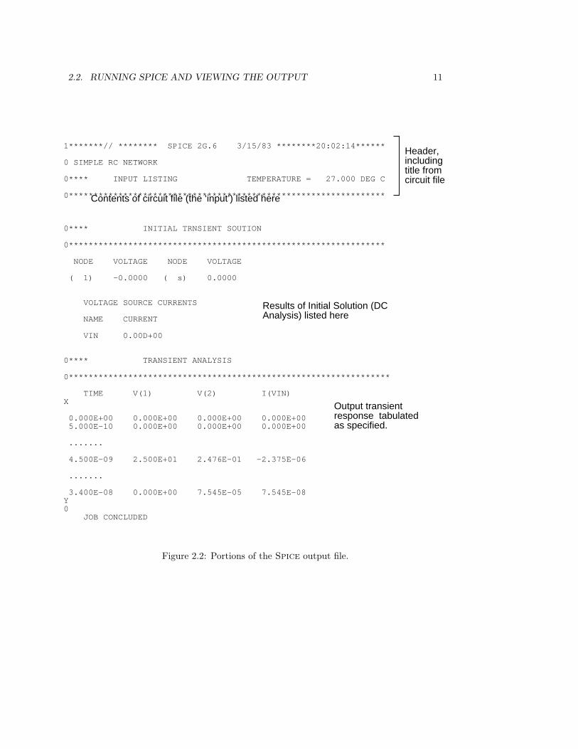
2.2. RUNNING SPICE AND VIEWING THE OUTPUT 11
1*******// ******** SPICE 2G.6 3/15/83 ********20:02:14******
0 SIMPLE RC NETWORK
0**** INPUT LISTING TEMPERATURE = 27.000 DEG C
0****************************************************************
0**** INITIAL TRNSIENT SOUTION
0****************************************************************
NODE VOLTAGE NODE VOLTAGE ( 1) -0.0000 ( s) 0.0000
VOLTAGE SOURCE CURRENTS
NAME CURRENT
VIN 0.00D+00
0**** TRANSIENT ANALYSIS
0*****************************************************************
TIME V(1) V(2) I(VIN)X
0.000E+00 0.000E+00 0.000E+00 0.000E+00 5.000E-10 0.000E+00 0.000E+00 0.000E+00
....... 4.500E-09 2.500E+01 2.476E-01 -2.375E-06
.......
3.400E-08 0.000E+00 7.545E-05 7.545E-08Y0 JOB CONCLUDED
Header,includingtitle fromcircuit file
Contents of circuit file (the ‘input’) listed here
Results of Initial Solution (DCAnalysis) listed here
Output transientresponse tabulated as specified.
Figure 2.2: Portions of the Spice output file.
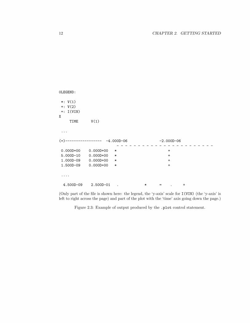
12 CHAPTER 2. GETTING STARTED
0LEGEND:
*: V(1)+: V(2)=: I(VIN)
XTIME V(1)
...
(=)----------------- -4.000D-06 -2.000D-06- - - - - - - - - - - - - - - - - - - - - - -
0.000D+00 0.000D+00 * +5.000D-10 0.000D+00 * +1.000D-09 0.000D+00 * +1.500D-09 0.000D+00 * +
....
4.500D-09 2.500D-01 . * = . +
(Only part of the file is shown here: the legend, the ‘y-axis’ scale for I(VIN) (the ‘y-axis’ isleft to right across the page) and part of the plot with the ‘time’ axis going down the page.)
Figure 2.3: Example of output produced by the .plot control statement.
2.3. ERROR MESSAGES 13
-0.2
0
0.2
0.4
0.6
0.8
1
1.2
1.4
1.6
0 5 10 15 20 25 30 35
Voltage (V)
Time (ns)
V(1)
V(2)
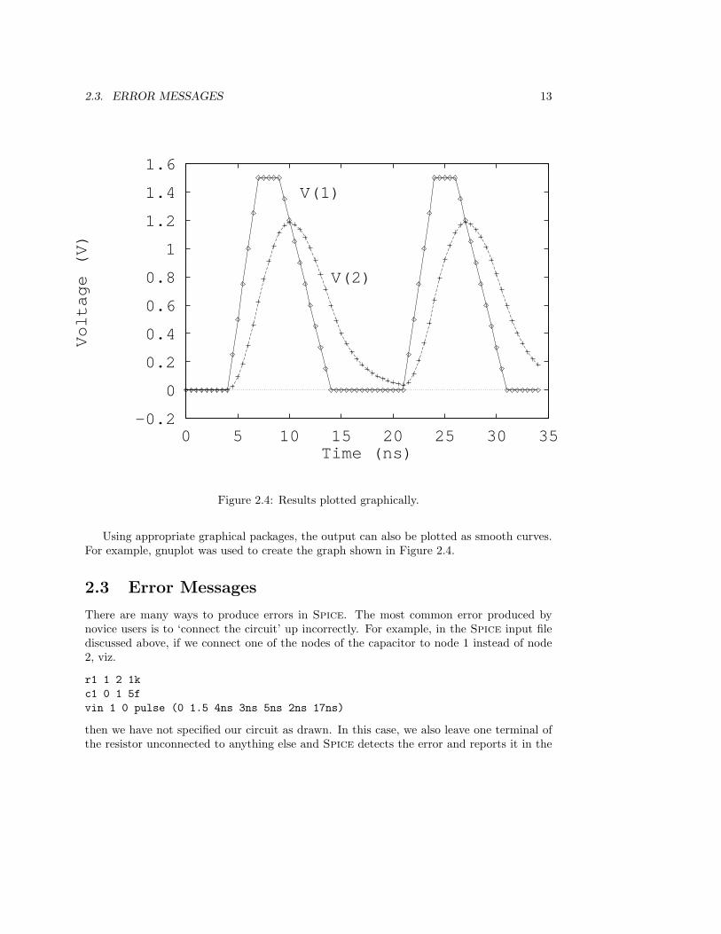
Figure 2.4: Results plotted graphically.
Using appropriate graphical packages, the output can also be plotted as smooth curves.For example, gnuplot was used to create the graph shown in Figure 2.4.
2.3 Error Messages
There are many ways to produce errors in Spice. The most common error produced bynovice users is to ‘connect the circuit’ up incorrectly. For example, in the Spice input filediscussed above, if we connect one of the nodes of the capacitor to node 1 instead of node2, viz.
r1 1 2 1kc1 0 1 5fvin 1 0 pulse (0 1.5 4ns 3ns 5ns 2ns 17ns)
then we have not specified our circuit as drawn. In this case, we also leave one terminal ofthe resistor unconnected to anything else and Spice detects the error and reports it in the

14 CHAPTER 2. GETTING STARTED
output file:
0*ERROR*: LESS THAN 2 CONNECTIONS AT NODE 2
However, life is rarely so simple. In a complex circuit it is always easy to get one nodenumber wrong on one element but leave all of the nodes connected to two or more elements.In this case Spice might detect no errors. If the output looks ‘wrong’ for any reason, thefirst thing to do is to draw your circuit by looking at the Spice file as written and checkthat against your intended circuit.
Another important thing to remember about error messages is that Spice is not verygood at drawing attention to them. Spice output files tend to be long and are crypticlooking. Error and Warning messages can be found almost anywhere within them. Readthe entire file. Errors are discussed further in Chapter 3 and Appendix E.
Chapter 3
Carrying On
In this chapter, we introduce the different element and control statement lines that Spiceallows you to use, starting with the different types of circuit elements. In particular wediscuss inductors, active elements (diodes and transistors), and transmission lines. Wethen cover the different types of analyses you can do with Spice, starting with the mostcommon, the transient analysis, which is introduced in Chapter 2. The main role of thecontrol statements is to specify these analyses.
Each implementation of Spice differs in the range of elements and control statementsused. In this chapter, we describe those elements and control statements found in all versionsof Spice, i.e. those found in Spice2g6.
3.1 Elements
Resistors and capacitors are described briefly in Chapter 2. We now look at the otherelements, both passive and active. The most common form of the element is described only.For example, we do not describe how a temperature dependency could be specified. Thatsort of detail is found in the reference section (chapters 6 and 7).
3.1.1 Inductors and Mutual Inductors
An example showing an inductor and a mutual inductor is shown below:15

16 CHAPTER 3. CARRYING ON
1
2
3
4
5
L1
L2 L3
M1
20 nH
40 nH 40 nH
k=0.9
L1 1 2 20nHL2 3 2 40nHL3 4 5 40nHK L1 L2 0.90
Note how the ‘dot’ is placed on the first node of each inductor.
3.1.2 Active Devices
Unlike passive devices, such as resistors, active, or semiconductor, devices can not be speci-fied by one or a few parameter values. To save typing effort a separate .model line is createdfor every semiconductor device type that might appear in the circuit. In this part of thetutorial, we do not describe the meaning of the parameters in the model line. That can befound in the Reference section (chapters 6 and 7). Instead, we give examples showing howsemiconductor devices are inserted into a Spice circuit. We only describe the bipolar junc-tion diode, bipolar junction transistor, and the MOS field effect transistor. Spice can alsobe used to describe junction field effect transistors and Gallium Arsenide but the process isthe same.
Diodes and Bipolar Transistors
The schematic and partial Spice net-list for a simple TTL inverter is shown in Figure 3.1.Note the following features in this circuit description:
• The format for bipolar junction transistors is:Qname NCollector NBase NEmitter [NSubstrate] ModelName [Area] [OFF]+ [IC=Vbe,Vce]specifying a three terminal device.
• The format for diodes is: Dname n1 n2 ModelName [Area] [OFF] [IC=VD ]specifying a two terminal device.

3.1. ELEMENTS 17
1
0
5
2
3
4
6
7Q1 Q2
Q3
R1 R2
R3
R4
1k 1.4k
100
1k
Q4
D1IN
OUT
Circuit described below
8
Q3 7 4 0 NQ1AD1 8 7 DPNQ4 6 3 8 NQ1AR4 5 6 100** Model element for NPN Transistor type NQ1A (courtesy Signetics).MODEL NQ1A NPN IS= 1.95E-17 BF= 7.03E+01 VAF= 1.80E+01 IKF= 1.80E-02
(Remainder of model deleted)
* Model for diode type DPN.MODEL DPN D(IS= 8.17E-17 RS= 2.85E+01 N= 9.99E-01 CJO= 1.65E-13+ VJ= 8.01E-01 M= 4.61E-01 EG= 7.99E-01 XTI= 4.00E+00)
Figure 3.1: TTL Circuit Description.
18 CHAPTER 3. CARRYING ON
• The use of ‘+’s in the model lines to ‘join’ different lines in the file into one line forSpice.
It is also possible to have an ‘area’ parameter in the diode and bipolar transistor element line.This area parameter is a scale factor, not an absolute measure. An area of ‘1.0’ (which is thedefault) specifies that the model parameters are used unchanged. Specifying another areafactor causes Spice to change some of the model parameters to reflect a larger or smallertransistor. An area of ‘2.0’ specifies a situation equivalent to two transistors operating inparallel.
MOSFETs
The MOSFET element line looks quite different than the element line for a bipolar transis-tor. There are two major differences, both of which are illustrated in Figure 3.2. First, theMOSFET is a four terminal device. Three of the terminals (source, drain, gate) have analo-gous functions to the three terminals in a bipolar transistor. The current passes between thedrain to the source (analogous to the emitter and collector) and is controlled by the voltageon the gate (analogous to the base). The fourth terminal is the ‘substrate’ referring to thebulk silicon in which the transistor sits. For correct functioning, the substrate must beconnected to the ground or Vcc node, for n-channel and p-channel transistors respectively.
The second major difference is that the physical dimensions of the transistor are spec-ified in the model line. Specifically, the channel length and width, and source and drainperimeters and areas are specified. These are the actual dimensions, as they appear on thechip. An example is shown in Figure 3.3. This example matches the usual general modelformat: Mname NDrain NGate NSsource NBulk ModelName [L=Length] [W=Width]
+ [AD=DrainDiffusionArea] [AS=SourceDiffusionArea]+ [PD=DrainPerimeter] [PS=SourcePerimeter]+ [OFF] [IC=VDS , VGS , VBS ]
where [] indicates optional parameters. PSpice supports additional element parameters.(For the full general format please see the reference catalog.)
Note that though the drain and source have different physical meanings (the source isthe source of the majority carrier – electrons for an n-channel [nmos] device and holes for ap-channel [pmos] device), no error is produced if they are interchanged in the Spice circuitdescription. For example, in figure 3.3, using M1 2 1 0 0 , produces the same simulationresults as using M1 0 1 2 0.
An example of a CMOS digital inverter circuit, together with its Spice model is givenin Figure 3.4. Note the use of the .option line in this example to fix circuit-wide defaultvalues for L, W, AD, and AS.
3.1.3 Transmission Lines
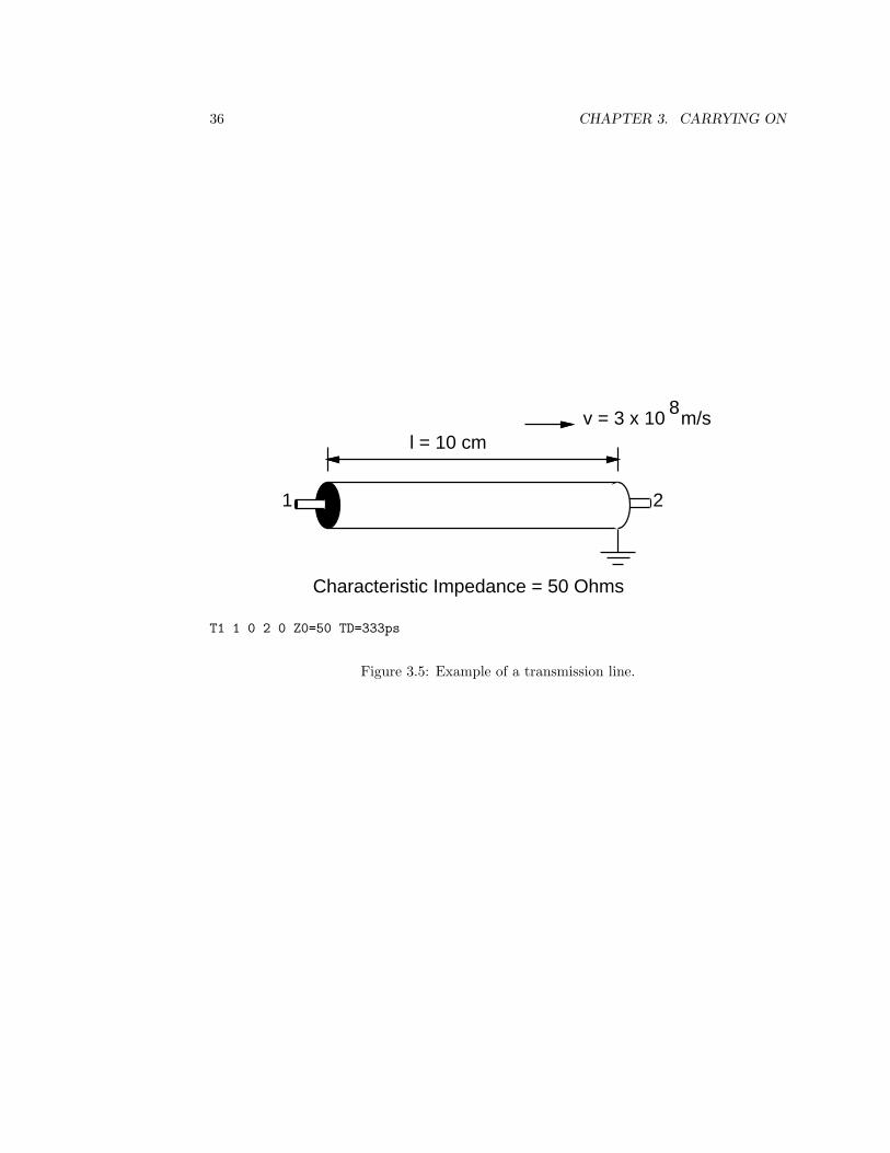
Though a transmission line is a four terminal device, two of the terminals are normally setto a common reference node, an example of which is shown in Figure 3.5. This losslesstransmission line model supports only a single mode of propagation. If the two ‘reference’terminals (nodes 0 in this example) correspond to two electrically different nodes in the

3.1. ELEMENTS 19
or Gate
Drain
Source
Gate
ChannelLength
ChannelWidth
Drain length
Drain Source
Channel
Bulk
Symbol
Top View
Side View
Source length
Gate
Drain
Source Bulk
Figure 3.2: Symbols used for a MOSFET and a top and side view of what a MOSFETtransistor looks like ‘in the silicon’.

20 CHAPTER 3. CARRYING ON
GateDrain Source
0.8 micron
1.2
mic
on
2 micron
Perimeter = 5.2 micron(‘pd’ and ‘ps’)
Area = 3.2 pm(‘ad’ and ‘as’)
2
M1 0 1 2 0 nenh l=0.8u w=1.6u ad=3.2p as=3.2p pd=5.2u ad=5.2u
Figure 3.3: Example of a MOSFET element specification.
physical circuit then two modes are excited and two transmission lines are required in thecorresponding Spice description.
If quick simulation times are important then it is necessary to limit the use of smalltransmission lines. In a transient simulation the minimum time step does not exceed halfthe propagation delay of the line. Smaller time steps result in longer simulation times. Ifthis is a problem, remember that a transmission line can be safely replaced by the equivalentlumped inductor and capacitor if the length of the line is smaller than 1/10th of the shortestsignal wavelength of interest.
3.1.4 Voltage and Current Sources
Independent Sources
Spice supplies a number of independent voltage and current source types. As many of thesource’s features only make sense in the context of the analysis to be used, only some of thesource’s features are discussed here. In particular, we present those features that might beused in a transient analysis (see Chapter 2 and Section 3.2.1).
Voltage supplies are specified using DC independent sources, for example:
VCC 5 0 DC 5
for a 5 V DC power supply between nodes 5 and 0.

3.1. ELEMENTS 21
Any repeating non-sinusoidal waveform can be specified using the pulse waveform spec-ification, an example of which was given in Chapter 2. pulse is often used to describe digitalclocks, for example.
Non-repeating non-sinusoidal waveforms are specified using the piece-wise linear (pwl)waveform function. One period of the pulse example presented in Chapter 2 is shown belowin the piece-wise linear format:
(0ns, 0V)
(4ns, 0V)
(7ns, 1.5V)(12ns, 1.5V)
(14ns, 0V)
(17ns, 0V)
vin 1 0 pwl (0ns 0V 4ns 0V 7ns 1.5V 12ns 1.5V 14ns 0V 17ns 0V)
22 CHAPTER 3. CARRYING ON
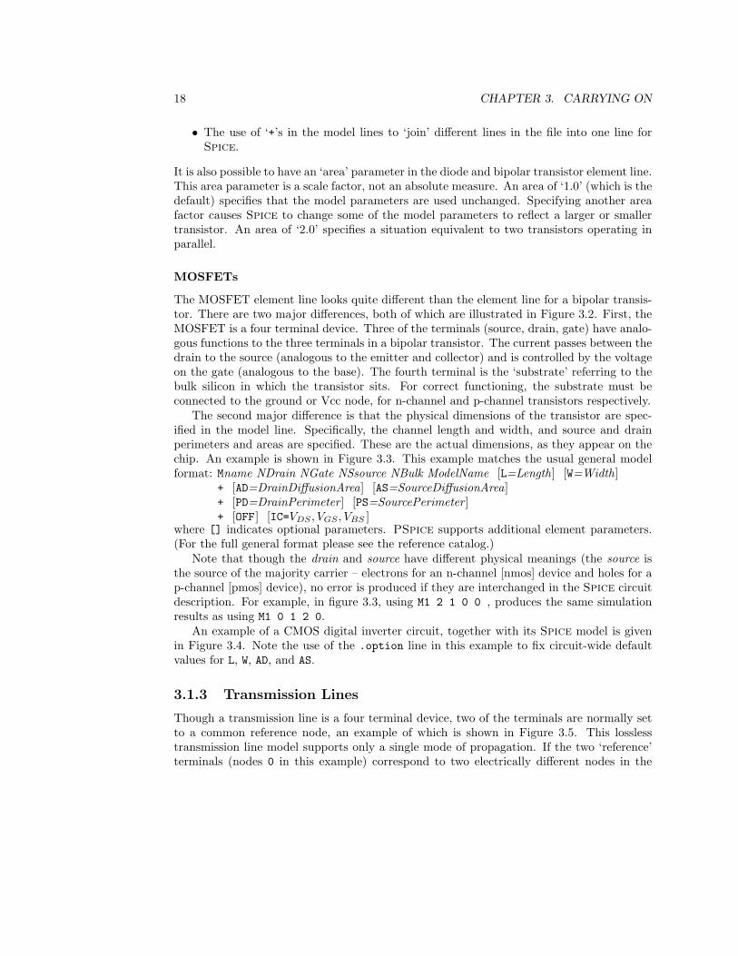
Sinusoidal and decaying sinusoidal waveforms are specified using the SIN function, forexample:
Vin 4 0 sin(2.5 1 100meg 10ns)
Time
Voltage
10 ns
100 MHz sinusoid
2.5
3.5
1.5
Spice also allows you to specify exponential and single-frequency FM signals. Please see thereference catalog for details.
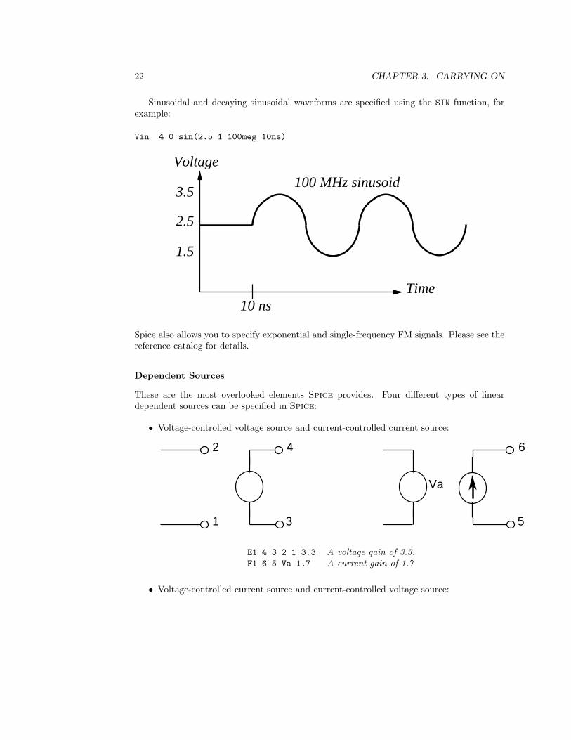
Dependent Sources
These are the most overlooked elements Spice provides. Four different types of lineardependent sources can be specified in Spice:
• Voltage-controlled voltage source and current-controlled current source:
1
2
3
4
Va
6
5
E1 4 3 2 1 3.3 A voltage gain of 3.3.F1 6 5 Va 1.7 A current gain of 1.7
• Voltage-controlled current source and current-controlled voltage source:

3.1. ELEMENTS 23
1
2
3
4
Va
6
5
V(2,1) G1 = 0.015 V(2,1)
I(Va)
H1 = 500 I(Va)
G1 4 3 2 1 15mmho A transconductance of 15×10−3mho (Ω−1).H1 6 5 Va 0.5k A transresistance of 500 Ohms
The above are linear sources. Non-linear sources can also be specified. For example, thefollowing voltage-controlled current source actually specifies a non-linear resistance thatcould be used as part of a non-linear Thevenin equivalent circuit:
1 2
Vthev V
0
Gout
out
Gout 2 1 2 0 0 1m -0.6m
The format used in this example is:
Gxxx node1 node2 ref-node1 ref-node2 C0 C1 C2
to produce a dependent source that obeys the equation:
I = C0 + C1(V (ref −node2)−V (ref −node1)) + C2(V (ref −node2)−V (ref −node1))2.
In this case, the equation specifying the current is:
I = 0 + 1× 10⁻³Vout − 0.6× 10⁻³V 2out
The above non-linear source is quadratic and dependent on only one other variable. Thesame format can be used to specify higher order polynomials. A source dependent on thevoltages/currents on/in ND other nodes/branches can be specified by including a poly(nd)statement in the element line. For example, the following linear voltage-controlled voltagesource specifies a gated sinusoidal source:
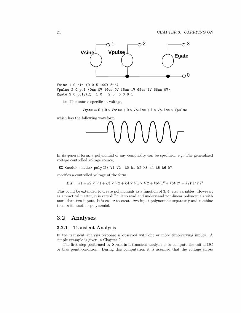
24 CHAPTER 3. CARRYING ON
2 31
0
Vsine VpulseEgate
Vsine 1 0 sin (0 0.5 100k 5us)Vpulse 2 0 pwl (0ns 0V 14us 0V 15us 1V 65us 1V 66us 0V)Egate 3 0 poly(2) 1 0 2 0 0 0 0 1
i.e. This source specifies a voltage,
Vgate = 0 + 0× Vsine + 0× Vpulse + 1× Vpulse× Vpulse
which has the following waveform:
In its general form, a polynomial of any complexity can be specified. e.g. The generalizedvoltage controlled voltage source,
EX <node> <node> poly(2) V1 V2 k0 k1 k2 k3 k4 k5 k6 k7
specifies a controlled voltage of the form
EX = k1 + k2× V 1 + k3× V 2 + k4× V 1× V 2 + k5V 12 + k6V 22 + k7V 12V 22
This could be extended to create polynomials as a function of 3, 4, etc. variables. However,as a practical matter, it is very difficult to read and understand non-linear polynomials withmore than two inputs. It is easier to create two-input polynomials separately and combinethem with another polynomial.
3.2 Analyses
3.2.1 Transient Analysis
In the transient analysis response is observed with one or more time-varying inputs. Asimple example is given in Chapter 2.
The first step performed by Spice in a transient analysis is to compute the initial DCor bias point condition. During this computation it is assumed that the voltage across
3.2. ANALYSES 25
capacitors is zero, the current through inductors is zero, and the value for dependent sourcesis zero. Spice then conducts the transient simulation by calculating all of the voltages andcurrents at a set of points in time. In the rest of this section, we discuss a number of issuesrelated to transient analyses, starting with a treatment of convergence.
DC Convergence
During both the DC analysis and the following transient analysis iterative numerical tech-niques are used to obtain a solution. The objective of these techniques is to iterate on thevalue of the node voltages and branch currents until successive iterations only bring verysmall changes in their values, i.e. Spice converges on a solution in the DC analysis and atevery time step.
Sometimes Spice can not converge on a solution. If this occurs during the DC analysisit will report this problem in the output file with a ‘convergence problem’ message like.Failure to converge in the DC analysis is usually due to an error in specifying node num-bers, circuit values or model parameter values. These should be checked carefully beforeproceeding further. However, sometimes Spice is having a genuine problem in convergingand you might have to help it find a solution.
In many bistable circuits (e.g. flip-flops) and positive feedback circuits, Spice will notconverge in the DC analysis or will converge to an undesirable value (e.g. midway betweenlogic-0 and logic-1 in a latch). One way to help Spice converge to the correct value is touse the off option to turn off devices in the feedback path, e.g.,
M0 0 1 2 0 pd=5.2u ad=5.2u off
allowing Spice to find a DC solution. Spice turns the devices back on during the transientanalysis. Another approach is to use nodeset to provide ‘hints’ to Spice or to specify initialconditions that force a solution.
Nodeset and Initial Conditions
The basic difference between using nodeset and specifying initial conditions is that the latterforces nodes to the specified voltage while nodeset only provides hints. The values specifiedby the nodeset line are only used during the first part of the DC solution procedure andthen ignored in the later parts. Thus if they are incorrect, or inconsistent, convergence isnot prevented. As an example of nodeset, ts use as follows in the the simple latch, willresult in the output (node 2) converging to 5 V (assuming a CMOS latch):
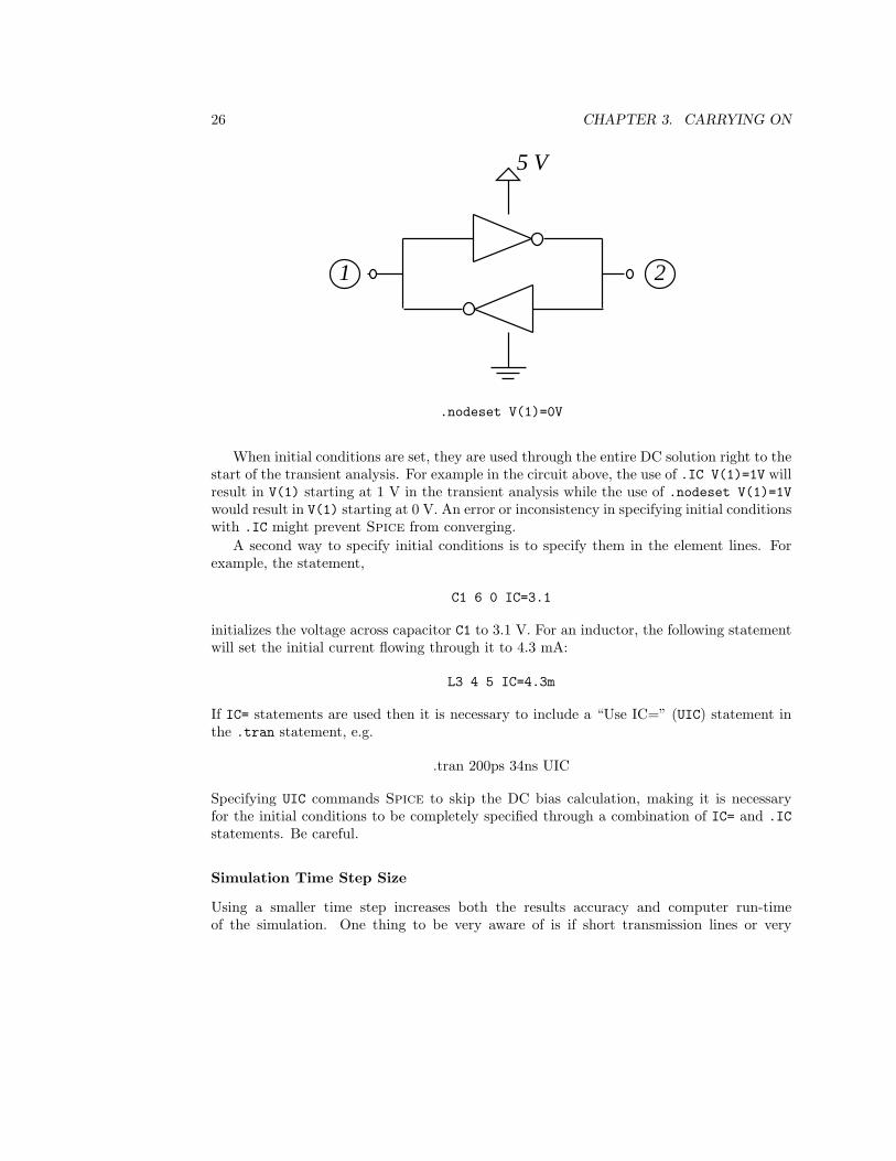
26 CHAPTER 3. CARRYING ON
1 2
5 V
.nodeset V(1)=0V
When initial conditions are set, they are used through the entire DC solution right to thestart of the transient analysis. For example in the circuit above, the use of .IC V(1)=1V willresult in V(1) starting at 1 V in the transient analysis while the use of .nodeset V(1)=1Vwould result in V(1) starting at 0 V. An error or inconsistency in specifying initial conditionswith .IC might prevent Spice from converging.
A second way to specify initial conditions is to specify them in the element lines. Forexample, the statement,
C1 6 0 IC=3.1
initializes the voltage across capacitor C1 to 3.1 V. For an inductor, the following statementwill set the initial current flowing through it to 4.3 mA:
L3 4 5 IC=4.3m
If IC= statements are used then it is necessary to include a “Use IC=” (UIC) statement inthe .tran statement, e.g.
.tran 200ps 34ns UIC
Specifying UIC commands Spice to skip the DC bias calculation, making it is necessaryfor the initial conditions to be completely specified through a combination of IC= and .ICstatements. Be careful.
Simulation Time Step Size
Using a smaller time step increases both the results accuracy and computer run-timeof the simulation. One thing to be very aware of is if short transmission lines or very
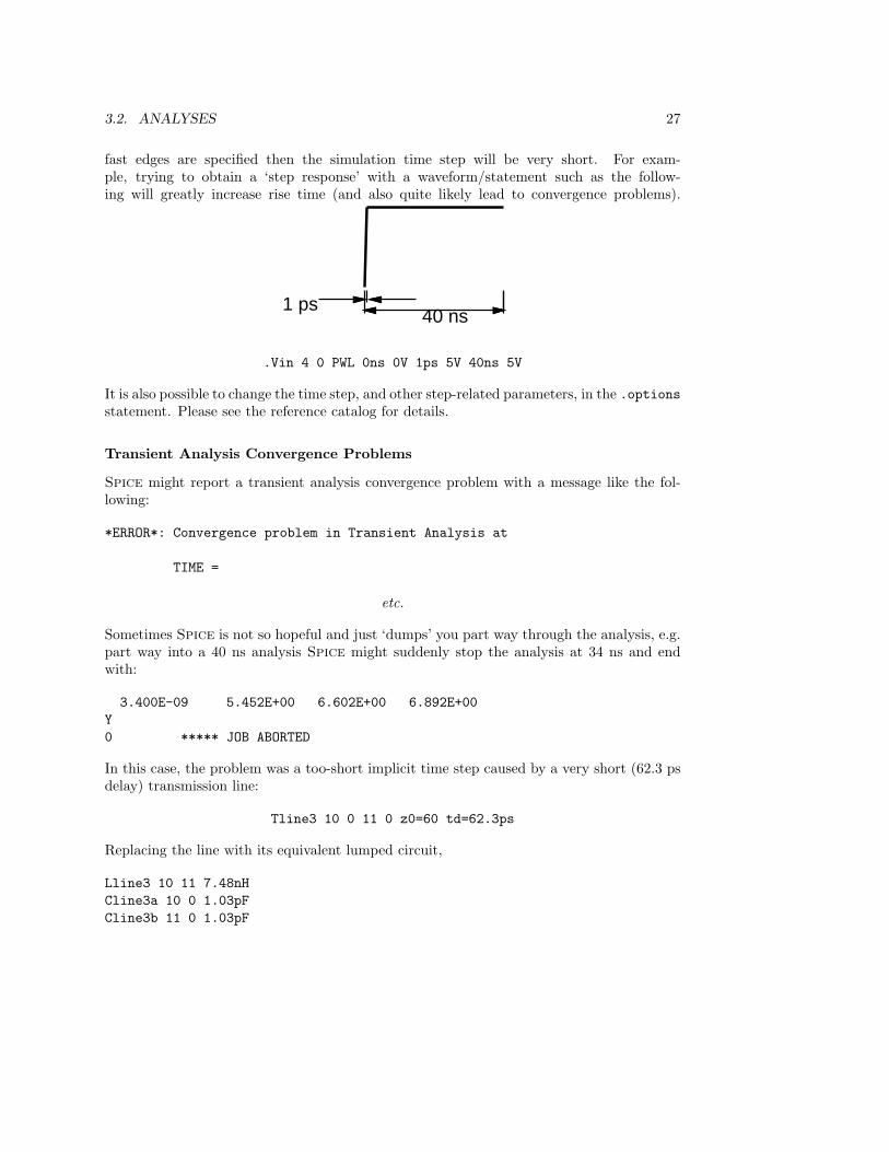
3.2. ANALYSES 27
fast edges are specified then the simulation time step will be very short. For exam-ple, trying to obtain a ‘step response’ with a waveform/statement such as the follow-ing will greatly increase rise time (and also quite likely lead to convergence problems).
1 ps40 ns
.Vin 4 0 PWL 0ns 0V 1ps 5V 40ns 5V
It is also possible to change the time step, and other step-related parameters, in the .optionsstatement. Please see the reference catalog for details.
Transient Analysis Convergence Problems
Spice might report a transient analysis convergence problem with a message like the fol-lowing:
*ERROR*: Convergence problem in Transient Analysis at
TIME =
etc.
Sometimes Spice is not so hopeful and just ‘dumps’ you part way through the analysis, e.g.part way into a 40 ns analysis Spice might suddenly stop the analysis at 34 ns and endwith:
3.400E-09 5.452E+00 6.602E+00 6.892E+00Y0 ***** JOB ABORTED
In this case, the problem was a too-short implicit time step caused by a very short (62.3 psdelay) transmission line:
Tline3 10 0 11 0 z0=60 td=62.3ps
Replacing the line with its equivalent lumped circuit,
Lline3 10 11 7.48nHCline3a 10 0 1.03pFCline3b 11 0 1.03pF
28 CHAPTER 3. CARRYING ON
solved the problem.If your transient analysis convergence problem is not being caused by a too short a
time step, then it is most likely caused by an error in specifying a circuit node number orparameter value. Your circuit and .model lines should be checked carefully. Often lookingat the circuit description as specified in the output listing is more useful than looking at thefile you typed in, as the output listing is describing what Spice ‘sees’.
However, Spice is a numerical program and can be quirky. For example, one simulationdriven by the pulse
V2 4 0 Pulse(0V 5V 0n 1.2n 1.2n 20n 40n)
would abort about half way through the simulation. However, turning the pulse ‘up-side-down’ (interchanging 0V and 5V),
V2 4 0 Pulse(5V 0V 0n 1.2n 1.2n 20n 40n)
allowed the simulation to complete.
Spectral Analysis – Fourier Transform
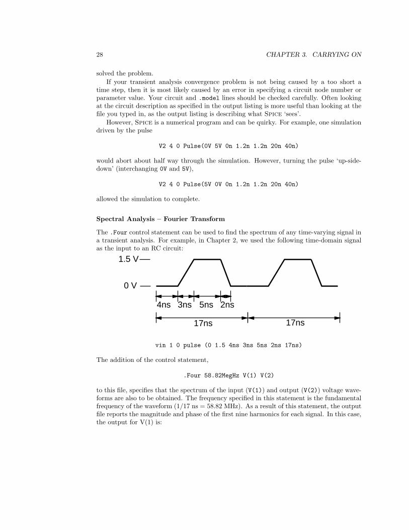
The .Four control statement can be used to find the spectrum of any time-varying signal ina transient analysis. For example, in Chapter 2, we used the following time-domain signalas the input to an RC circuit:
1.5 V
0 V
4ns 3ns 5ns 2ns
17ns 17ns
vin 1 0 pulse (0 1.5 4ns 3ns 5ns 2ns 17ns)
The addition of the control statement,
.Four 58.82MegHz V(1) V(2)
to this file, specifies that the spectrum of the input (V(1)) and output (V(2)) voltage wave-forms are also to be obtained. The frequency specified in this statement is the fundamentalfrequency of the waveform (1/17 ns = 58.82 MHz). As a result of this statement, the outputfile reports the magnitude and phase of the first nine harmonics for each signal. In this case,the output for V(1) is:
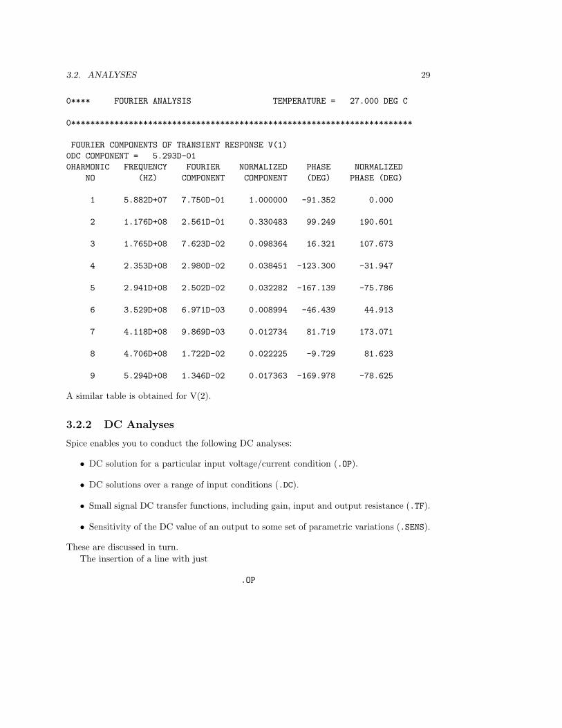
3.2. ANALYSES 29
0**** FOURIER ANALYSIS TEMPERATURE = 27.000 DEG C
0***********************************************************************
FOURIER COMPONENTS OF TRANSIENT RESPONSE V(1)0DC COMPONENT = 5.293D-010HARMONIC FREQUENCY FOURIER NORMALIZED PHASE NORMALIZED
NO (HZ) COMPONENT COMPONENT (DEG) PHASE (DEG)
1 5.882D+07 7.750D-01 1.000000 -91.352 0.000
2 1.176D+08 2.561D-01 0.330483 99.249 190.601
3 1.765D+08 7.623D-02 0.098364 16.321 107.673
4 2.353D+08 2.980D-02 0.038451 -123.300 -31.947
5 2.941D+08 2.502D-02 0.032282 -167.139 -75.786
6 3.529D+08 6.971D-03 0.008994 -46.439 44.913
7 4.118D+08 9.869D-03 0.012734 81.719 173.071
8 4.706D+08 1.722D-02 0.022225 -9.729 81.623
9 5.294D+08 1.346D-02 0.017363 -169.978 -78.625
A similar table is obtained for V(2).
3.2.2 DC Analyses
Spice enables you to conduct the following DC analyses:
• DC solution for a particular input voltage/current condition (.OP).
• DC solutions over a range of input conditions (.DC).
• Small signal DC transfer functions, including gain, input and output resistance (.TF).
• Sensitivity of the DC value of an output to some set of parametric variations (.SENS).
These are discussed in turn.The insertion of a line with just
.OP
30 CHAPTER 3. CARRYING ON
on it asks Spice to determine the DC bias point of the circuit with inductors shorted andcapacitors opened, just the same as the DC analysis conducted before a transient analysis.It might be used in situations where you wish to know the DC bias point but the analysisyou are doing does not request it (e.g. such as when determining a frequency response).
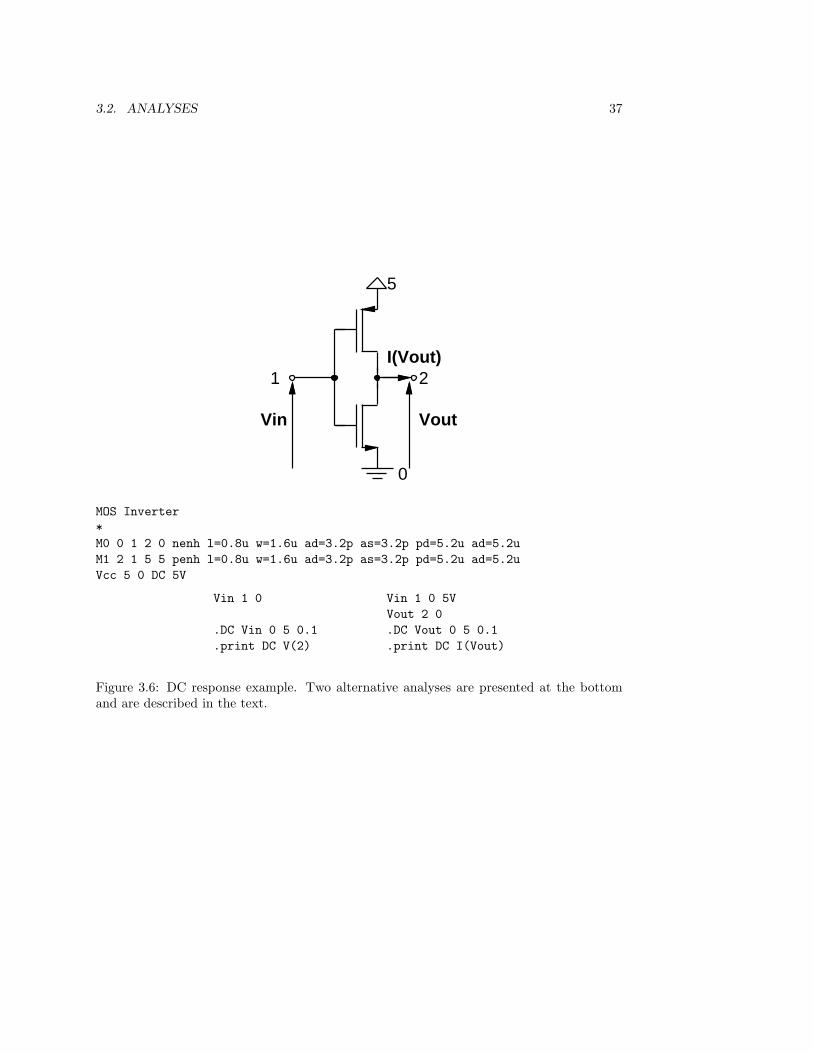
A command line beginning with .DC instructs Spice to sweep the specified voltagesource over the specified range, reporting the DC bias point for each combination of inputconditions. If more than one source is specified in the .DC statement, then the first sourcewill be swept over its entire range for every value of the second source. An example is givenin Figure 3.6 in which two analyses alternatives are presented at the bottom. The left handalternative instructs Spice to plot the transfer characteristics of the CMOS inverter, theright hand example instructs Spice to plot the output V-I characteristics for when Vin is5 V. Both examples specify that the voltage sweep is to be from 0 to 5 V in 0.1 V increments.The resulting output V-I characteristic (obtained using the statements on the right handside of the Figure 3.6) is plotted in Figure 3.7.
Now, if you wish to find the small signal output resistance at say Vout = X V,
rout =∂v
∂i
∣∣∣∣Vout=X V
then one way to obtain this would be to measure the slope of the plot shown in Figure 3.7at Vout = 0.5 V. However, Spice provides an easier way to get this result as a transferfunction .TF:
.TF I(vout) Vout
There is no need for a .print statement with .TF. Running this produces the output:
OUTPUT RESISTANCE AT I(VOUT) = 2.247D+03
A DC sweep can also be done by specifying a slow moving input and a conducting atransient analysis. Sometimes this is necessary, for example in circuits with hysteresis, suchas a Schmitt Trigger.
Sometimes we wish to know the sensitivities of various output parameters with respectto variations in circuit parameters. For example, we might wish to know whether to specifyresistors to +/-10% or +/-1% in order to guarantee a certain bias point in a transistoramplifier. This is done with the .sens statement. The following example determines thesensitivity of the bias point of an amplifier to variations in resistance values:
3.2. ANALYSES 31
0
5
3
4
Q1
R1
R2RE1
40k
40k100
RC14k
Cbuff100uF
1 2I(Vbase)
6Vin
Extract from input file:
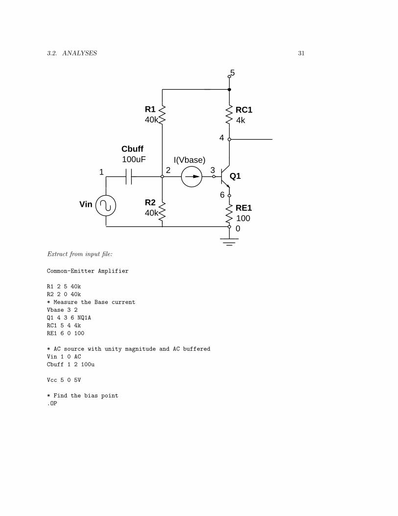
Common-Emitter Amplifier
R1 2 5 40kR2 2 0 40k* Measure the Base currentVbase 3 2Q1 4 3 6 NQ1ARC1 5 4 4kRE1 6 0 100
* AC source with unity magnitude and AC bufferedVin 1 0 ACCbuff 1 2 100u
Vcc 5 0 5V
* Find the bias point.OP
32 CHAPTER 3. CARRYING ON
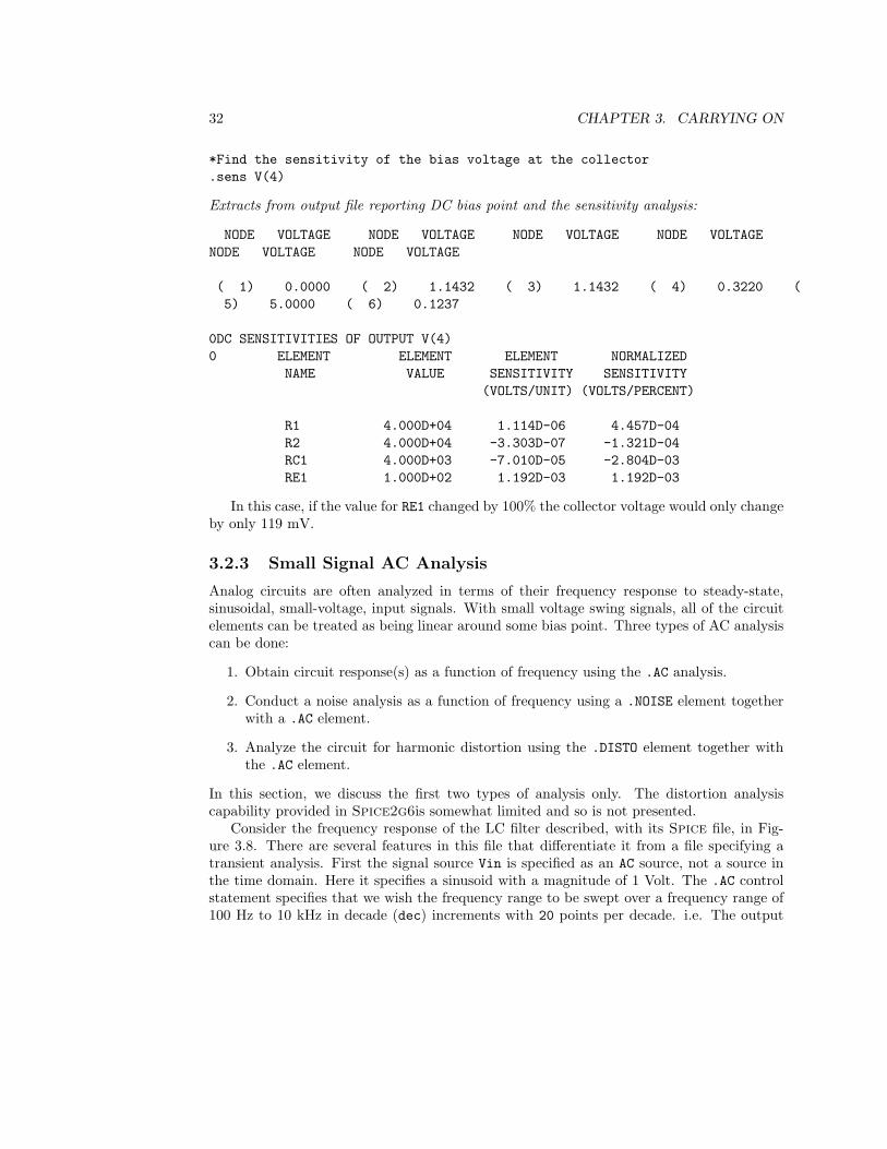
*Find the sensitivity of the bias voltage at the collector.sens V(4)
Extracts from output file reporting DC bias point and the sensitivity analysis:
NODE VOLTAGE NODE VOLTAGE NODE VOLTAGE NODE VOLTAGENODE VOLTAGE NODE VOLTAGE
( 1) 0.0000 ( 2) 1.1432 ( 3) 1.1432 ( 4) 0.3220 (5) 5.0000 ( 6) 0.1237
0DC SENSITIVITIES OF OUTPUT V(4)0 ELEMENT ELEMENT ELEMENT NORMALIZED
NAME VALUE SENSITIVITY SENSITIVITY(VOLTS/UNIT) (VOLTS/PERCENT)
R1 4.000D+04 1.114D-06 4.457D-04R2 4.000D+04 -3.303D-07 -1.321D-04RC1 4.000D+03 -7.010D-05 -2.804D-03RE1 1.000D+02 1.192D-03 1.192D-03
In this case, if the value for RE1 changed by 100% the collector voltage would only changeby only 119 mV.
3.2.3 Small Signal AC Analysis
Analog circuits are often analyzed in terms of their frequency response to steady-state,sinusoidal, small-voltage, input signals. With small voltage swing signals, all of the circuitelements can be treated as being linear around some bias point. Three types of AC analysiscan be done:
1. Obtain circuit response(s) as a function of frequency using the .AC analysis.
2. Conduct a noise analysis as a function of frequency using a .NOISE element togetherwith a .AC element.
3. Analyze the circuit for harmonic distortion using the .DISTO element together withthe .AC element.
In this section, we discuss the first two types of analysis only. The distortion analysiscapability provided in Spice2g6is somewhat limited and so is not presented.
Consider the frequency response of the LC filter described, with its Spice file, in Fig-ure 3.8. There are several features in this file that differentiate it from a file specifying atransient analysis. First the signal source Vin is specified as an AC source, not a source inthe time domain. Here it specifies a sinusoid with a magnitude of 1 Volt. The .AC controlstatement specifies that we wish the frequency range to be swept over a frequency range of100 Hz to 10 kHz in decade (dec) increments with 20 points per decade. i.e. The output
3.2. ANALYSES 33
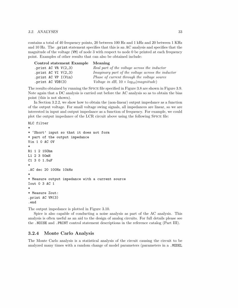
contains a total of 40 frequency points, 20 between 100 Hz and 1 kHz and 20 between 1 KHzand 10 Hz. The .print statement specifies that this is an AC analysis and specifies that themagnitude of the voltage (VM) of node 3 with respect to node 0 be printed at each frequencypoint. Examples of other results that can also be obtained include:
Control statement Example Meaning.print AC VR V(2,3) Real part of the voltage across the inductor.print AC VI V(2,3) Imaginary part of the voltage across the inductor.print AC VP I(Vin) Phase of current through the voltage source.print AC VDB(3) Voltage in dB, 10× log10(magnitude)
The results obtained by running the Spice file specified in Figure 3.8 are shown in Figure 3.9.Note again that a DC analysis is carried out before the AC analysis so as to obtain the biaspoint (this is not shown).
In Section 3.2.2, we show how to obtain the (non-linear) output impedance as a functionof the output voltage. For small voltage swing signals, all impedances are linear, so we areinterested in input and output impedance as a function of frequency. For example, we couldplot the output impedance of the LCR circuit above using the following Spice file:
RLC filter** ‘Short’ input so that it does not form* part of the output impedanceVin 1 0 AC 0V*R1 1 2 15OhmL1 2 3 50mHC1 3 0 1.5uF*.AC dec 20 100Hz 10kHz** Measure output impedance with a current sourceIout 0 3 AC 1** Measure Zout:.print AC VM(3).end
The output impedance is plotted in Figure 3.10.Spice is also capable of conducting a noise analysis as part of the AC analysis. This
analysis is often useful as an aid to the design of analog circuits. For full details please seethe .NOISE and .PRINT control statement descriptions in the reference catalog (Part III).
3.2.4 Monte Carlo Analysis
The Monte Carlo analysis is a statistical analysis of the circuit causing the circuit to beanalyzed many times with a random change of model parameters (parameters in a .MODEL
34 CHAPTER 3. CARRYING ON
statement). It is available in the PSpice version only.The form on the Monte Carlo analysis is
PSpice92Form
.MC NumberOfRuns AnalysisType OutputSpecification OutputFunction [LIST]+ [OUTPUT( OutputSampleType )] [RANGE(LowValue, HighValue)]+ [SEED=SeedValue]
Monte Carlo analysis repeates DC analysis as specified by the .DC statement, AC small-signal analysis as specified by the .AC statement, or transient analysis as specified by the.TRAN statement. In the .MC statement the way in which the results of the multiple runsare interested is controlled by the OutputSpecification] and OutputFunction parameters.
A typical use of Monte Carlo analysis is to predict yield of a circuit by examining theeffect of process variations such as length and width of transistors. As well the effect oftemperature on circuit performance can be investigated.
The initial run uses the nominal parameter values given in the NETLIST. Subsequentruns statistically vary model parameters indicated as having either lot or device tolerances.These tolerances are specified in a .MODEL statement.
3.2.5 Transfer Function Specification
The transfer function specifies a small-signal DC analysis from which a small-signal transferfunction and input and output resistances are computed. The transfer function computed isthe ratio of the DC value of the output quantity to the input quantity. In the above examplesthe following transfer functions are computed:
EXAMPLE Transfer Function
.TF V(10) VINPUT V(10)VINPUT
.TF V(10,2) ISOURCE V(10, 2)ISOURCE
.TF I(VLOAD) ISOURCE I(VLOAD)ISOURCE
3.2.6 Parameteric Analysis
3.2.7 Sensistivity and Worst Case Analysis

3.2. ANALYSES 35
1 2
5
0
CMOS Inverter Example*M0 0 1 2 0 nenh l=0.8u w=1.6u ad=3.2p as=3.2p pd=5.2u ad=5.2uM1 5 1 2 5 penh l=0.8u w=1.6u ad=3.2p as=3.2p pd=5.2u ad=5.2uVcc 5 0 DC 5V** following option line fixes transistor length and width, and* drain/source area defaults*.options defl=0.8u defw=1.6u defad=3.2p defas=3.2p**.model nenh nmos+ Level=2 Ld=4.000e-8 Tox=1.750000e-08+ Nsub=1.506725e+17 Vto=0.59073 Kp=6.124495e-05
(Remainder of model omitted.)
.model penh pmos+ Level=2 Ld=4.000000e-08 Tox=1.750000e-08
(Remainder of model omitted.)
Figure 3.4: A CMOS inverter.
36 CHAPTER 3. CARRYING ON
1 2
l = 10 cmv = 3 x 10 m/s8
Characteristic Impedance = 50 Ohms
T1 1 0 2 0 Z0=50 TD=333ps
Figure 3.5: Example of a transmission line.
3.2. ANALYSES 37
1 2
5
0
VoutVin
I(Vout)
MOS Inverter*M0 0 1 2 0 nenh l=0.8u w=1.6u ad=3.2p as=3.2p pd=5.2u ad=5.2uM1 2 1 5 5 penh l=0.8u w=1.6u ad=3.2p as=3.2p pd=5.2u ad=5.2uVcc 5 0 DC 5V
Vin 1 0 Vin 1 0 5VVout 2 0
.DC Vin 0 5 0.1 .DC Vout 0 5 0.1
.print DC V(2) .print DC I(Vout)
Figure 3.6: DC response example. Two alternative analyses are presented at the bottomand are described in the text.
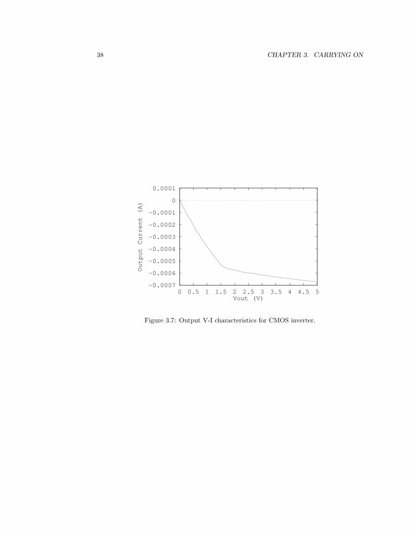
38 CHAPTER 3. CARRYING ON
-0.0007
-0.0006
-0.0005
-0.0004
-0.0003
-0.0002
-0.0001
0
0.0001
0 0.5 1 1.5 2 2.5 3 3.5 4 4.5 5
Output Current (A)
Vout (V)
Figure 3.7: Output V-I characteristics for CMOS inverter.

3.2. ANALYSES 39
Vin (f)
R1
C1
150
1.5uF
0
12
V(3)
3L1 50mH
RLC filter*Vin 1 0 AC 1V AC signal source*R1 1 2 15OhmL1 2 3 50mHC1 3 0 1.5uF*.AC dec 20 100Hz 10kHz AC analysis specification*.print AC VM(3) print results of AC analysis
Figure 3.8: LC filter and the Spice file specifying a frequency response analysis. (Commentsin emphasis are not part of the file.)

40 CHAPTER 3. CARRYING ON
0
1
2
3
4
5
6
7
8
9
10
100 1000 10000
Vout/Vin
Frequency (Hz)
Figure 3.9: Frequency response of the circuit shown in Figure 3.8.
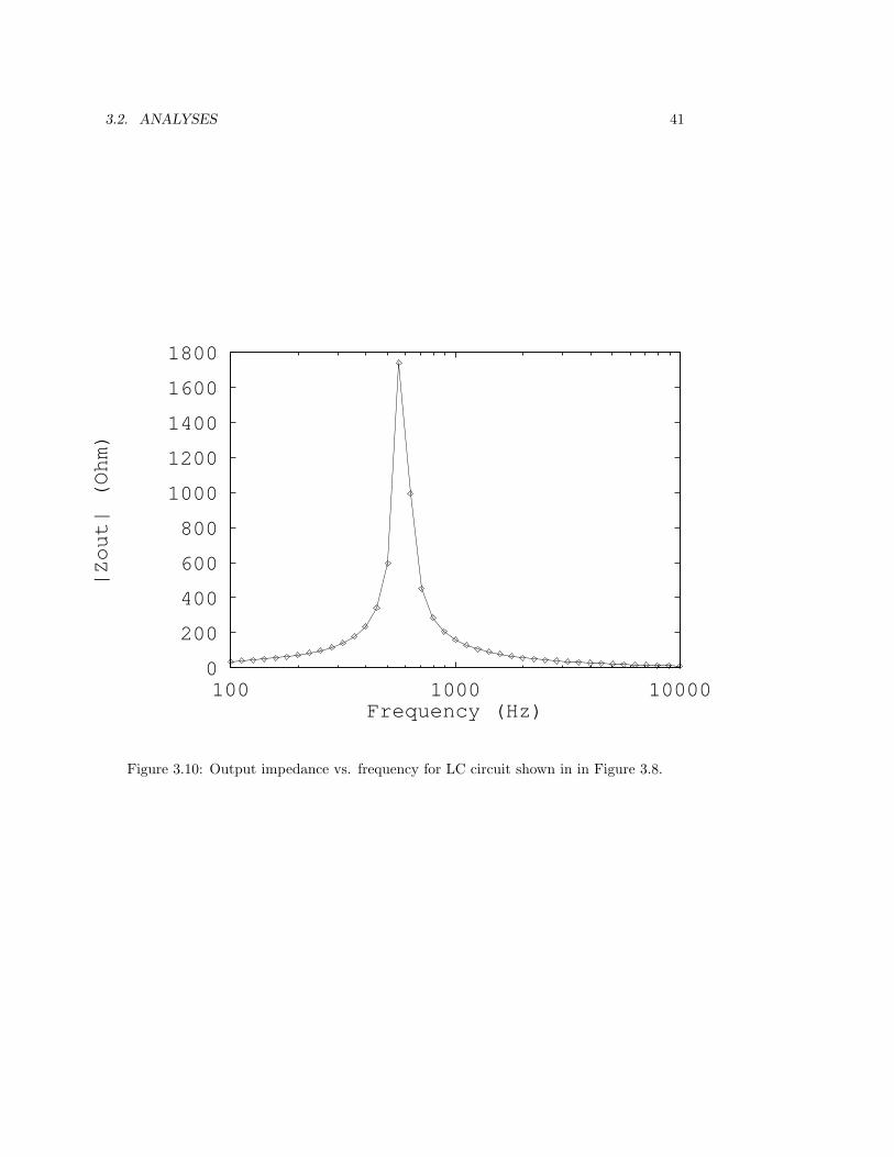
3.2. ANALYSES 41
0
200
400
600
800
1000
1200
1400
1600
1800
100 1000 10000
|Zout| (Ohm)
Frequency (Hz)
Figure 3.10: Output impedance vs. frequency for LC circuit shown in in Figure 3.8.

42 CHAPTER 3. CARRYING ON
Chapter 4
How Spice Works
4.1 Introduction
Spice has three basic analyses: DC analysis — initiated by the .DC statement; AC analysis —initiated by the .AC statement; and transient analysis — initiated by the .TRAN statement.AC analysis involves incorporating the relations relating terminal voltages and device currentsinto a matrix equation This matrix equation is called the network equation and embodies thetopology of the network and the constitutive relations (that is, device equation) describingindividual devices. It derives from a mathematical statement of Kirchoff’s current lawwith device currents replaced by node voltages with the substitution achieved by using theconstitutive relations of individual devices. Extensions to this basic form of the networkequation (called the modal formulation of the network equation) is required for elementsthat can not be mathematicly modeled as a current or currents in terms of voltages. ACanalysis is the appropriate place to begin a technical exposition of the analysis algorithmsin Spice as it illustrates the method of development of network equation is used by all otheranalyses.
Transient analysis requires, as well, that a time-stepping numerical integration algorithmbe incorporated into the network equations. A straight forward approach to transient anal-ysis, which was used prior to the development of the “Spice” approach, is to derive thestate equations in state space (that is in differential form using the s operator) and applythe time discretization of a numerical integration method to the complete network equation.However, in Spice the time discretization is incorporated in the constitutive relations beforethe network equation is developed. The time discretized network equation must be solvediteratively and the Newton iteration procedure is applied to the device equations along withthe time-discretization step. This has proved to be a particularly robust approach and isthe main reason Spice is so widely accepted.
43
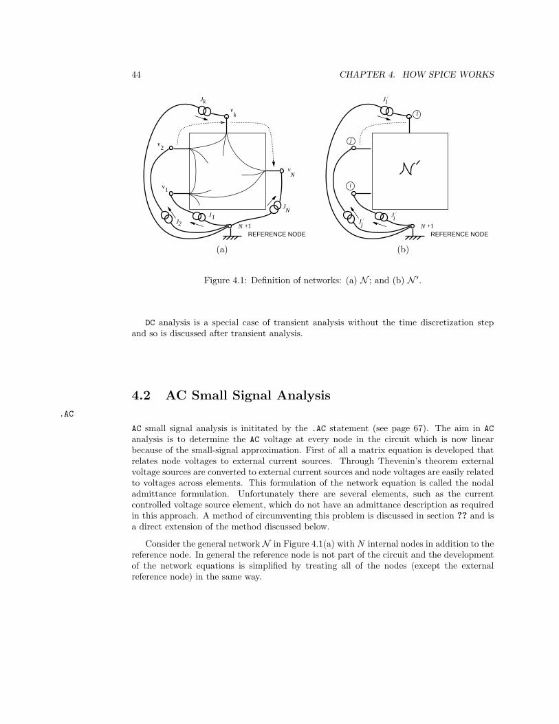
44 CHAPTER 4. HOW SPICE WORKS
N +1REFERENCE NODE
vN
vk
v
v
2
1
Jk
JJ
21
NJ
N +1REFERENCE NODE
J
JJ
i
j
l
ij
l
/
/
/
(a) (b)
Figure 4.1: Definition of networks: (a) N ; and (b) N ′.
DC analysis is a special case of transient analysis without the time discretization stepand so is discussed after transient analysis.
4.2 AC Small Signal Analysis
.AC
AC small signal analysis is inititated by the .AC statement (see page 67). The aim in ACanalysis is to determine the AC voltage at every node in the circuit which is now linearbecause of the small-signal approximation. First of all a matrix equation is developed thatrelates node voltages to external current sources. Through Thevenin’s theorem externalvoltage sources are converted to external current sources and node voltages are easily relatedto voltages across elements. This formulation of the network equation is called the nodaladmittance formulation. Unfortunately there are several elements, such as the currentcontrolled voltage source element, which do not have an admittance description as requiredin this approach. A method of circumventing this problem is discussed in section ?? and isa direct extension of the method discussed below.
Consider the general network N in Figure 4.1(a) with N internal nodes in addition to thereference node. In general the reference node is not part of the circuit and the developmentof the network equations is simplified by treating all of the nodes (except the externalreference node) in the same way.
4.3. DC ANALYSIS 45
All of the nodes of the network have external current sources J with Jn being theexternal current source between the n th node and the reference node. In practice most ofthe external current sources, the J ’s, are zero and those that are not are due to independentsources. The network equations used in Spice relate the node voltages, the v’s, and the J ’s.In matrix form
Yvn = Jn (4.1)
where vn is the vector of node voltages, and Jn is the vector of external currents. Solution ofequation (??) enablEs the node voltages to be evaluated given the external current sources.
In Spice the grounded reference node, node “0”, is part of the network and so thereis a linear dependence of the rows of Y (|Y| = 0). Hence Y is called the indefinite nodaladmittance matrix. One row and one column can be deleted from Y without the lossing anyinformation to yield what is called the definite nodal admittance matrix. For now considerthat the reference node is an arbitrary node. The correction required because the referencenode is actually part of the circuit is discussed in section ??.
4.3 DC Analysis.DC
The analysis of nonlinear resistive circuits, or equivalently the analysis of circuits at DCis an important first step in ACand transient analysis. In both cases nonlinear resistiveanalysis determines the initial starting point for further analysis incorporating energy storageelements such as capacitors and inductors.
DC analysis is Spice is identical to transient analysis discussed in the previous sectionexcept that the contributions of capacitors and inductors are ignored. DC analysis hasbetter convergence properties ithan transient analysis since energy storage elements, andthus resonant responses, are eliminated. As well the analysis is numericly efficient sinceonly a steady-state response is required and calculated.
4.4 Discussion
Spice supports several analyses other than those discussed above. Essentially these areextensions of the AC, DC and transient analyses.
The transfer function analysis, initiated by the .TF statement, calculates a transferfunction as the ratio of the DC value of an output quantity to the DC value of an inputquantity over a range of values of the input quantity. A DC analysis at each value of theinput quantity is performed.
With the .DISTO statement a distortion analysis is performed by dteremining the steady-state harmonic and intermodulation products for small input signal. Evaluation of thesmall-signal distortion is based on a third-order multi-dimensional Volterra series expansionof nonlinearities around their operating point. The method for calculating of the distortionproducts parallels AC analysis algorithm.
46 CHAPTER 4. HOW SPICE WORKS
The sensitivity analysis calculates the DC small-signal sensitivities of each output quantitywith respect to every circuit parameter. It is initiated by the .SENS statement. The transferfunction computed is the sensitivity (or partial derivative) of the DC value of the outputquantity with respect to the each and every circuit parameter.
If the .NOISE statement is included in the input file the noise generated by active devicesand resistors is evaluated. All active devices and some passive devices have noise modelsconsisting of uncorrelated noise current sources. These noise current sources are used asthe external current sources in ACanalysis. One noise source at a time is considered and theresponse at the output terminals and sources specified are calculated. The contributionsfrom each source are added in a root-mean-squared sense as they are uncorrelated. Thenoise analysis utilizes the network equation formulated and solved in AC analysis.
A Monte Carlo analysis is performed when the .MC statement is specified. In the MonteCarlo analysis either a DC, an AC, or a transient analysis is performed multiple times.
An operating point analysis initiated by the .OP statement is just a single DCanalysis.The Fourier analysis performed when the .FOUR statement is used is not really a separate
analysis at all. Really it is a way of examiing the results of a transient analysis by takingthe Fourier transform of a voltage or current response.
4.5 To Explore Further
The essential aspects of Spice are the models of devices and the algorithms for formulatingand solving the network equations. The derivation of the AC model of devices is straight-forward requiring the y parameters of the device. These are obtained from the analyticderivatives of the device equations calculated at the operating point of the circuit as de-termined from a DC analysis. For transient and DC analysis the associated discrete circuitmodel must be calculated from the device equations. The device equations of semiconduc-tor devices are calculated from knowledge of the device physics. Derivation of the modelsused for semiconductor devices in Spice2g6 and Spice3 are described in [2] (SemiconductorDevice Modeling with SPICE edited by P. Antognetti and G. Massobrio). Without fail themodels in Spice2g6 are available in all commercial versions of Spice. Spice3 and mostcommercial versions of Spice provide additional or enhanced models. Derivations of moreadvanced models are described in [8] (Semiconductor Device Modeling for VLSI by K. Lee,M. Shur, T. Fjeldly and T. Ytterdal).
In Spice the network equations are stored in sparse matrices to conserve memory usage.This also results in much faster solution of the network equations than if regular matriceswere used. Greater detail than that provided in this chapter of the numerical algorithmsused in Spice can be found in [1] (Fundamentals of Computer-Aided Circuit Simulation,”by W. J. McCalla).
Chapter 5
Input File
5.1 Introduction
The operation of Spice is controlled by statements which are embedded in an input filewhich includes as well descriptions of elements and their topology. The description of theelements and their topology is also known as a netlist. The output or results of a Spice netlistrun are logged in an output file and in more modern versions of Spice, in a data file forsubsequenct interactive plotting anad analysis. With PSpice the prgram for subsequentanalysis is probe and with Spice3 the comparable tool is NUTMEG.
5.2 Circuit Model
The model used by Spice to represent circuits is as shown in Figure 5.1. Spice supports modelsubcircuitsa hierarchical description of a circuit with subcircuits. A large number of parameters are
required for many elements, especially for active devices, and for these the model conceptis introduced where most of the parameters of active elements can be defined separatelyfrom invocation of the element. This permits a single model description to be used by manyelements. A model is specific to a particular element type but not all elements have models.Mostly models are used to set the parameters describing a semiconductor fabrication processand so are common to many elements.
47

48 CHAPTER 5. INPUT FILE
TOPLEVELCIRCUITDESCRIPTION
MODEL 1
MODEL 2
MODEL 4
MODEL 3
SUBCIRCUIT ADESCRIPTION
SUBCIRCUIT CDESCRIPTION
SUBCIRCUIT BDESCRIPTION
NETLIST
A EXPANSION
A.B EXPANSION
A.B.C EXPANSION
A.C EXPANSION
C EXPANSION
INTERNAL CIRCUITREPRESENTATION
CONTROLSTATEMENTS
Figure 5.1: The Spice circuit representation.
5.3. INPUT LINES 49
When the input file is read subcircuits definitions and models are stored internally sep-arately from the main circuit. Subcircuit calls are expanded if the subcricuits referencedare already defined and stored internally. If a referenced subcircuit is not defined thenthe subcircuit call is flagged as not being expanded and only when the input file has beencompletely read (up to the .END statement) is an attempt made to resolve incomplete expan-sions. In PSpice library files (described in the .LIB statement discussion on page 85) arechecked. The first time a library file is to be searched, an internal table of which subcircuitsand models are available and where they can be found in the library files is constructed.Models are treated in a similar way, a model is used if it has been defined otherwise resolvedreferences to models are expanded once the input file has been completely scanned (up tothe .END statement). With PSpice evaluation of expressions in subcircuits and models isonly performed when on fully expanded subcircuits. Note that expressions and libraries arenot supported in Spice2g6or in Spice3.
5.3 Input Lines
The input file of Spice is essentially unstructured. It must begin with a TITLE line and titleshould end in a .END statement although this is automaticlly assumed if the end of the .endinput file is read. The string on the TITLE line is used as the banner in the output logfile appearing at the top of each page. The .END statement marks the end of one circuitwith the effect that several circuits can be specified in the file (at least for Spice3 andPSpice). In between the TITLE line and the .END statement can be any mix of statements— which control the operation of the simulator and the analysis to be performed; optionalcomment lines — for documenting the input file; and element lines — which specify thecircuit elements. The input file can in fact contain no statements and the simulator willthen perform an operating point .OP analysis. Spice does not distinguish between upperand lower case characters.
Except for the TITLE line which is the first line of the input file, the type of input linesis distinguished by the first character on the line: statements begin with a period “.”;element lines begin with an alphabetic character “A–Z” — with the letter identifying theelement type (e.g. R for a resistor); and comment lines begin with an asterisk “*”. Inolder terminology, based on the original use of punched cards, statements are referred to as“dot cards” or “statement cards”; element lines are referred to as “element cards” or “devicecards”; and comment lines as “comment cards.”
50 CHAPTER 5. INPUT FILE
PSpice allows for in line comments indicated by a semicolon “;”. The semicolon andeverything following it on the same line are ignored except for purpose of echoing the inputfile in the output log file.
5.3.1 Analysis Statements
An analysis statement identifies the type of analysis to be performed. Any combination ofanalyses may be specified. Reporting of the results of an analysis is controlled by the .PRINT,.PLOT and, in with PSpiceby the .PROBE control statements. If no analysis statement isincluded in the input file then an operating point analysis (.OP) is performed by default. Abrief description of the analysis options and the page on which a complete description canbe found as follows.
.AC AC Analysis . . . . . . . . . . . . . . . . . . . . . . . . . . . . . . . . . . . . . . . . . . . Page 67
Obtains the small-signal circuit response as a function of frequency. The .AC analysis is oneof several small signal AC analyses.
.DC DC Analysis . . . . . . . . . . . . . . . . . . . . . . . . . . . . . . . . . . . . . . . . . . . Page 70
DC solutions over a range of input conditions (.DC). .DISTO Small-Signal Dis-
tortion Analysis Spice2g6 and Spice3 Only . . . . . . . . . . . . . . . . . . . . . . . . . . . . . . . Page 74
Analyze the circuit for harmonic and intermodulation distortion. This analysis is availablein Spice2g6 and Spice3 but is not available in PSpice as it has proved to be unreliable.In Spice2g6 the distortion analysis must be performed in conjunction with a .AC analysis.
.FOUR Fourier Analysis . . . . . . . . . . . . . . . . . . . . . . . . . . . . . . . . . . . . . . . Page 81
The .FOUR control statement can be used to find the spectrum of any time-varying signalin a (.TRAN) transient analysis. The .FOUR statement is unlike other analysis statementsas it does not initiate a simulation but interprets the result of a simulation initiated by the.TRAN sattement.
.MC Monte Carlo Analysis (PSpice only) . . . . . . . . . . . . . . . . . . . Page 87
The Monte Carlo analysis is a statistical analysis of the circuit causing the circuit to beanalyzed many times with a random change of model parameters (parameters in a .MODELstatement). The analyses specified in the .DC, .AC or .TRAN statements can be simulatedmultiple times.
.NOISE Small-Signal Noise Analysis . . . . . . . . . . . . . . . . . . . . . . . . . . . . Page 96
Conduct a small-signal noise analysis as a function of frequency. In PSpice this statementmust be used in conjunction with a .AC statement.
.OP Operating Point Analysis . . . . . . . . . . . . . . . . . . . . . . . . . . . . . . Page 99
DC solution for a particular input voltage/current condition. This is the default analysis ifno analysis is specified in the input file. This is the default analysis if not analysis type isspecified in the input file.
.PZ Pole-Zero Analysis, Spice3 Only . . . . . . . . . . . . . . . . . . . . . . . Page 123
5.3. INPUT LINES 51
In this analysis the poles and zeros of the small signal ACtransfer function of a two-port isevaluated. .SAVEBIAS Save Bias Conditions . . . . . . . . . . . . . . . . . . . . . . Page 125
.SENS Sensitivity Analysis . . . . . . . . . . . . . . . . . . . . . . . . . . . . . . . . . . . . Page 126
The sensitivity of the DC value of an output to some set of parametric variations is calcu-lated.
.STEP Parameteric Analysis PSpice92 Only . . . . . . . . . . . . . . . . . . Page 127
.TF Transfer Function Specification PSpice Only . . . . . . . . . . Page 133
Small signal DC transfer functions, including gain and input and output resistance arecomputed
.TRAN Transient Analysis . . . . . . . . . . . . . . . . . . . . . . . . . . . . . . . . . . . . . Page 135
In the transient analysis response is observed with one or more time-varying inputs.
.WCASE Sensistivity and Worst Case Analysis PSpice92 Only . . Page 138
5.3.2 Control Statements
.DISTRIBUTION Distribution Specification (PSpice only) . . . . . . . . . . . . . . . Page 77
This statement specifies the statistical tolerance distribution used in a Monte Carlo analysis(see the .MC statement on page 87).
.END End Statement . . . . . . . . . . . . . . . . . . . . . . . . . . . . . . . . . . . . . . . . Page 79
This statement indicates the end of the input of one circuit.
.ENDS End Subcircuit Statement . . . . . . . . . . . . . . . . . . . . . . . . . . . . . . Page 80
The end subcircuit statement indicates the end of a subcircuit definition.
.FUNC Function Definition PSpice92Only . . . . . . . . . . . . . . . . . . . . Page 82
Enables commonly used expressions to be more conveniently defined as functions.
.IC Initial Conditions . . . . . . . . . . . . . . . . . . . . . . . . . . . . . . . . . . . . . . Page 83
This statement is used to set initial conditions for transient analysis. It has no effect onother types of analyses.
.INC Include Statement, PSpice only . . . . . . . . . . . . . . . . . . . . . . . Page 84
Specifies the name of a file which is to be treated as part of the input file.
.LIB Library Statement, PSpice only . . . . . . . . . . . . . . . . . . . . . . . Page 85
Specifies the name of a library file.
.MODEL Model Statement . . . . . . . . . . . . . . . . . . . . . . . . . . . . . . . . . . . . . . Page 90
52 CHAPTER 5. INPUT FILE
Specifies the parameters of elements that either are too numerous to put on the element lineor are common to many elements.
.NODESET Node Voltage Initialization . . . . . . . . . . . . . . . . . . . . . . . . . . . . . Page 95
Specifies the voltage at one or more nodes to be used as an initial guess.
.OPTIONS Option Specification . . . . . . . . . . . . . . . . . . . . . . . . . . . . . . . . . . . Page 100
The options specification provides the user control over the program and sets defaults forcertain elements and analyses.
.PARAM Parameter Definition, PSpice92 Only . . . . . . . . . . . . . . . . . Page 106
This statement defines parameters that can be used in subsequent statements and elementlines.
.PLOT Plot Specification . . . . . . . . . . . . . . . . . . . . . . . . . . . . . . . . . . . . . . Page 108
The plot specification controls the information that is plotted in the output file as a characterplot. This is one way to view the result of various analyses.
.PRINT Print Specification . . . . . . . . . . . . . . . . . . . . . . . . . . . . . . . . . . . . . Page 113
The print specification controls the information that is reported as the result of variousanalyses.
.PROBE Data Output Specification, PSpice Only . . . . . . . . . . . . . . . Page 121
This statement saves the node voltages and device currents in a file for subsequent interactiveplotting
.SUBCKT Subcircuit Statement . . . . . . . . . . . . . . . . . . . . . . . . . . . . . . . . . . Page 128
Indicates the start of a subcircuit description and describes int interface to the subcircuit.
.TEMP Temperature Specification . . . . . . . . . . . . . . . . . . . . . . . . . . . . . Page 131
Specifies the temperature(s) to perform the analysis at.
.TEXT Text Parameter Definition, PSpice92 Only . . . . . . . . . . . . Page 132
.WATCH Watch Analysis Statement PSpice92 Only . . . . . . . . . . . . . Page 137
.WIDTH Width Specification . . . . . . . . . . . . . . . . . . . . . . . . . . . . . . . . . . . . Page 141

5.3. INPUT LINES 53
Specifies the column width for the output file.
5.3.3 Elements
The general form for elements is device name, followed by a list of nodes, followed by thenumeric value of the element, followed in some cases by the name of a model, and then byother keywords:
Name Node1 Node2 . . . NodeN NumericValue ModelName+ keyword=NumericValue . . . InitialConditions.
For some elements initial conditions (InitialConditions) can also be specified which can beused to ensure that the desired initial state of astable circuits is obtained and also to aid inconvergence. The first letter of the Name identifies the element. For example, if Name isRTEST then the element is a resistor.
The general form above is not the form for every element. The way in which Spiceevolved resulted in the syntax for element lines not being fully consistent. Commercialextensions, as with PSpice, allowing alphabetic names for nodes rather than just an integerdesignation also result in syntaxical problems. With this extension it is not possible to usethe fact that a field was alphabetic to distinguish between a node and a parameter name.However this change has necessitated no change to the the standard syntax as definedby Spice2g6. The problem appears in conjunction with other extensions which allow foran arbitrary number of nodes in some statements. The result is that the syntax can beslightly different than would be expected. For these reasons the description of the form ofa particular element or statement must be consulted to ensure that the syntax is correct.
Passive Elements
The passive devices supported in Spice2g6, Spice3 and PSpice and where their descrip-tions can be found are as follows:
C Capacitor . . . . . . . . . . . . . . . . . . . . . . . . . . . . . . . . . . . . . . . . . . . . . . . . . . . . . . . . . Page 182
K Mutual Inductor . . . . . . . . . . . . . . . . . . . . . . . . . . . . . . . . . . . . . . . . . . . . . . . . . . Page 221
L Inductor . . . . . . . . . . . . . . . . . . . . . . . . . . . . . . . . . . . . . . . . . . . . . . . . . . . . . . . . . . Page 229
R Resistor . . . . . . . . . . . . . . . . . . . . . . . . . . . . . . . . . . . . . . . . . . . . . . . . . . . . . . . . . . . Page 283
S Voltage Controlled Switch . . . . . . . . . . . . . . . . . . . . . . . . . . . . . . . . . . . . . . . . . Page 286
W Current Controlled Switch . . . . . . . . . . . . . . . . . . . . . . . . . . . . . . . . . . . . . . . . . Page 306
Active Elements
Form
Qname NCollector NBase NEmitter [NSubstrate] ModelName [Area] [OFF]+ [IC=Vbe,Vce]
54 CHAPTER 5. INPUT FILE
Unlike passive devices active devices can not be specified by one or a few parametervalues. Since many of the parameter values are the same for many devices it is convenientto specify them in a .MODEL statement that can be reused many times. All active elementsrequire a .MODEL statement and most allow an optional substrrate node to be used on theelement line.
The active devices supported in Spice2g6, Spice3 and PSpice and where their de-scriptions can be found are as follows:
B GaAs MESFET (PSpice only) . . . . . . . . . . . . . . . . . . . . . . . . . . . . . . . . . . . . Page 145
(See Z element for Spice3equivalent) . . . . . . . . . . . . . . . . . . . . . . . . . . . . . . . . . . ??
D Diode . . . . . . . . . . . . . . . . . . . . . . . . . . . . . . . . . . . . . . . . . . . . . . . . . . . . . . . . . . . . . Page 186
J Junction Field-Effect Transistor . . . . . . . . . . . . . . . . . . . . . . . . . . . . . . . . . . . Page 212
M MOSFET . . . . . . . . . . . . . . . . . . . . . . . . . . . . . . . . . . . . . . . . . . . . . . . . . . . . . . . . . Page 231
Z MESFET . . . . . . . . . . . . . . . . . . . . . . . . . . . . . . . . . . . . . . . . . . . . . . . . . . . . . . . . . Page ??
(See B element for PSpice equivalent) . . . . . . . . . . . . . . . . . . . . . . . . . . . . . . . . . . . . . . . . . 145
5.3.4 Distributed Elements
The distributed devices and where they are described are as follows:
T Transmission Line . . . . . . . . . . . . . . . . . . . . . . . . . . . . . . . . . . . . . . . . . . . . . . . . . Page 290
U Lossy RC Transmission Line . . . . . . . . . . . . . . . . . . . . . . . . . . . . . . . . . . . . . . . . . . . ??
5.3.5 Source Elements
The sources supported and where they can be found are as follows:
E Voltage-Controlled Voltage Source . . . . . . . . . . . . . . . . . . . . . . . . . . . . . . . . . Page 191
F Current-Controlled Current Source . . . . . . . . . . . . . . . . . . . . . . . . . . . . . . . . Page 195
G Voltage-Controlled Current Source . . . . . . . . . . . . . . . . . . . . . . . . . . . . . . . . Page 197
H Current-Controlled Voltage Source . . . . . . . . . . . . . . . . . . . . . . . . . . . . . . . . Page 201
I Independent Current Source . . . . . . . . . . . . . . . . . . . . . . . . . . . . . . . . . . . . . . . Page 203
V Independent Voltage Source . . . . . . . . . . . . . . . . . . . . . . . . . . . . . . . . . . . . . . . Page 297
5.4. INPUT GRAMMAR 55
The control of the E, F, G and H elements can be control by a polynomial function ofvoltage or current.
5.3.6 Interface Elements
The interface elements supported and where they can be found are as follows:
N Digital Input Interface, PSpice only . . . . . . . . . . . . . . . . . . . . . . . . . . . . . . . Page ??
Interfaces digital analog simulation by providing a means for a state transistion to controlan analog response.
O Digital Output Interface, PSpice only . . . . . . . . . . . . . . . . . . . . . . . . . . . . . Page ??
Determines the equivalent digital state of an analog signal.
U Digital Device . . . . . . . . . . . . . . . . . . . . . . . . . . . . . . . . . . . . . . . . . . . . . . . . . . . . . 294
X Subcircuit Call . . . . . . . . . . . . . . . . . . . . . . . . . . . . . . . . . . . . . . . . . . . . . . . . . . . . Page 309
Interfaces a circuit (or subcircuit) to a subcircuit.
5.4 Input Grammar
Each input line contains fields which are delimited (separated) by one of a number of char-acters. The most obvious delimiter is simply a space but other characters are also treated Delimiteras “white space” characters. White space is defined as one or any combination of the White Spacefollowing characters:
“blank” “tab” ( ) , =While the above characters appear in the input file they are ignored except that they aretreated as a field delimiter. The “(”, “)”, “=” and “,” characters are often used in the inputfile and are included in specifiying the syntax for elements and statements but they serveonly to add visual structure to the input.
Continuation lines begin with a plus “+” in the first column. For example LineContinuationR1 1 2 1000
and R1 1 2+1000
are equivalent.Comment lines begin with an asterisk “*” in the first position. In line comments are sup-
ported in PSpice and these begin with a semicolon “;” and must be contained wholly on oneline. For example * This just shows off a comment
R1 1 2 1000 ;This shows of an in line comment
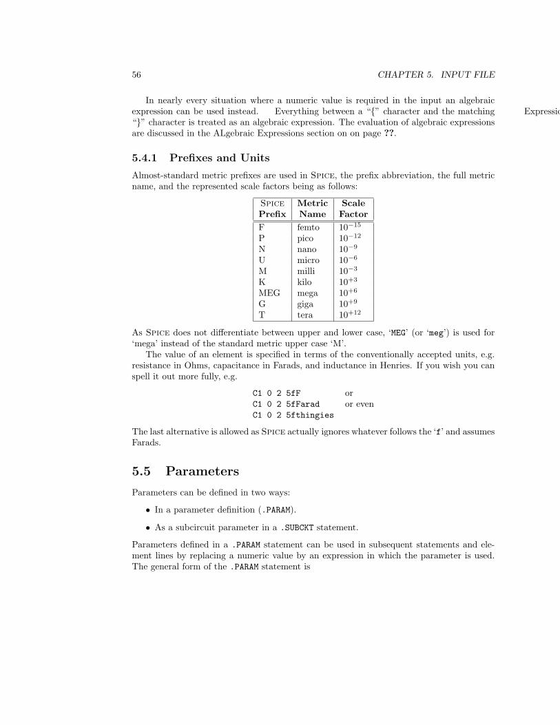
56 CHAPTER 5. INPUT FILE
In nearly every situation where a numeric value is required in the input an algebraicexpression can be used instead. Everything between a “” character and the matching Expression“” character is treated as an algebraic expression. The evaluation of algebraic expressionsare discussed in the ALgebraic Expressions section on on page ??.
5.4.1 Prefixes and Units
Almost-standard metric prefixes are used in Spice, the prefix abbreviation, the full metricname, and the represented scale factors being as follows:
Spice Metric ScalePrefix Name FactorF femto 10−15
P pico 10−12
N nano 10−9
U micro 10−6
M milli 10−3
K kilo 10+3
MEG mega 10+6
G giga 10+9
T tera 10+12
As Spice does not differentiate between upper and lower case, ‘MEG’ (or ‘meg’) is used for‘mega’ instead of the standard metric upper case ‘M’.
The value of an element is specified in terms of the conventionally accepted units, e.g.resistance in Ohms, capacitance in Farads, and inductance in Henries. If you wish you canspell it out more fully, e.g.
C1 0 2 5fF orC1 0 2 5fFarad or evenC1 0 2 5fthingies
The last alternative is allowed as Spice actually ignores whatever follows the ‘f’ and assumesFarads.
5.5 Parameters
Parameters can be defined in two ways:
• In a parameter definition (.PARAM).
• As a subcircuit parameter in a .SUBCKT statement.
Parameters defined in a .PARAM statement can be used in subsequent statements and ele-ment lines by replacing a numeric value by an expression in which the parameter is used.The general form of the .PARAM statement is
5.5. PARAMETERS 57
.PARAM [ParameterName = NumericValue . . . ]+ [ParameterName = Expression . . . ]
Here the ParameterName is the name of a parameter with the first character being al-phabetic (a-zA-Z) and can be assigned a numeric value NumericValue which may be fol-lowed immediately by a spice scale factor. For example, SMALL=1.E-9, SMALL=+1N,SMALL=1NV and SMALL=1.E-9V are equivalent and all establish a parameter SMALLwith a value of 10−9. If ParameterName is the name of a previously defined parameter atthe same level of subcircut expansion then the parameter value is changed. If the .PARAMstatement is is in the top level circuit then the parameter value is global and is available anywhere in the netlist. If the .PARAM statement is in a subcircuit then the parameter valueis local and can be used at the current subcircuit expansion level or lower in the subcircuitexpansion hierarchy. The same idea applies to values of a parameter changed in a subcir-cuit. Value changes are local and are available in the current subcircuit and lower nestedsubcircuits. Libraries are searched for parameters not defined in the circuit NETLIST or inincluded files. A .PARAM statement does not have to be within a subcircuit in a library.
Instead of a numeric value an algebraic expression can be used to establish the value ofthe parameter. The expression is evaluated in the standard way for an algebraic expressionreplacing numeric values and is evaluated at the time of expansion rather than as the netlistis read. This ensures the correct hierarchical interpretation of the netlist. The treatment ofexpression is discussed in section 5.6 on page 58. Note that as always the expression mustbe enclosed in matching braces ( . . . ).
Parameters can be used nearly anywhere a numeric value is expected by including themin an expression evaluation even if the expression contains a single parameter. For example
.PARAM rbig=10MEGR1 1 2 RBIG
establishes a resistance R1 between nodes 1 and 2 with a value of 106 Ω.
Several predefined parameters are supported and the user must avoid defining these asunpredictable results may result. The predefined parameters are
58 CHAPTER 5. INPUT FILE
Name Value DescriptionTEMP not supported Analysis temperature.
Reserved for future expansion
VT not supported Thermal voltage.Reserved for future expansion
5.6 Expressions
In PSpice most places where a numeric value is normally used an expression (within braces . . . ) can be used instead. An expression can contain any supported mathematicaloperation, constant numeric values or expressions. Exceptions are
• Polynomial coefficients.
• The values of the transmission line device parameters NL and F.
• The values of the piece-wise linear characteristic in the PWL form of the independentvoltage (V) and current (I) sources.
• The values of the resistor device parameter TC.
• As node numbers.
and
• Values of most statements (such as .TEMP, .AC, .TRAN etc.)
Specifically included are
• The values of all other device parameters.
• The values in .IC and .NODESET statements.
• The values in .SUBCKT statements.
and
• The values of all model parameters. F.
Operators that can be used in expressions are listed in Table 5.1.

5.6. EXPRESSIONS 59
Table 5.1: Expression operators.
Operator Syntax DescriptionPLUS x+y plusMINUS x-y minusUNARY PLUS +x unary plusUNARY MINUS -x unary minusMULTIPLY x*y multiplyDIVIDE y/x dividePOW x^y or x**y raise to a power, xy
AND x&y ANDOR x|y ORNOT !x NOTXOR x y XOR (exclusive or)SIN sin(x) sine, argument in radiansCOS cos(x) cosine, argument in radiansTAN tan(x) tangent, argument in radiansASIN asin(x) arcsine, argument in radiansACOS acos(x) arccosine, argument in radiansATAN atan(x) arctangent, argument in radiansSINH sinh(x) hyperbolic sineCOSH cosh(x) hyperbolic cosineTANH tanh(x) hyperbolic tangentEXP exp(x) exponentiation, ex
ASINH asinh(x) arc-hyberbolic sineACOSH acosh(x) arc-hyberbolic cosineATANH atanh(x) arc-hyberbolic tangentABS abs(x) absolute, |x|SQRT sqrt(x) square root,
√x
5.6.1 Polynomials
Polynomial expressions can be used with the controlled source elements (E, F, G and H) torealize nonlinear controlled sources. The specification of the polynomial must be at the endof the input line and has two forms. The polynomial format for a voltage-controlled currentsource (the G element) or a voltage-controlled voltage source (the E element) is
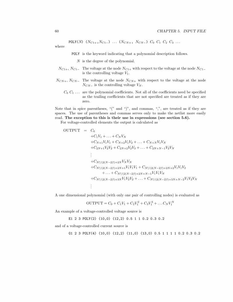
60 CHAPTER 5. INPUT FILE
POLY(N) (NC1+,NC1−) . . . (NCN+, NCN−) C0 C1 C2 C3 . . .where
POLY is the keyword indicating that a polynomial description follows.
N is the degree of the polynomial.
NC1+, NC1− The voltage at the node NC1+ with respect to the voltage at the node NC1−is the controlling voltage V1.
NCN+, NCN− The voltage at the node NCN+ with respect to the voltage at the nodeNCN− is the controlling voltage VN .
C0 C1 . . . are the polynomial coefficients. Not all of the coefficients need be specifiedas the trailing coefficients that are not specified are treated as if they arezero.
Note that in spice parentheses, “(” and “)”, and commas, “,”, are treated as if they arespaces. The use of parentheses and commas serves only to make the netlist more easilyread. The exception to this is their use in expressions (see section 5.6).
For voltage-controlled elements the output is calculated as
OUTPUT = C0
+C1V1 + . . . + CNVN
+CN+1V1V1 + CN+2V1V2 + . . . + CN+NV1VN
+C2N+1V2V2 + C2N+2V2V3 + . . . + C2N+N−1V2VN
...+CN !/(2(N−2)!)+2NVNVN
+CN !/(2(N−2)!)+2N+1V1V1V1 + CN !/(2(N−2)!)+2N+2V1V1V2
+ . . . + CN !/(2(N−2)!)+2N+N−1V1V1VN
+CN !/(2(N−2)!)+3NV1V2V2 + . . . + CN !/(2(N−2)!)+3N+N−2V1V2VN
...
A one dimensional polynomial (with only one pair of controlling nodes) is evaluated as
OUTPUT = C0 + C1V1 + C2V21 + C3V
31 + . . . CNV N
1
An example of a voltage-controlled voltage source is
E1 2 3 POLY(2) (10,0) (12,2) 0.5 1 1 0.2 0.3 0.2
and of a voltage-controlled current source is
G1 2 3 POLY(4) (10,0) (12,2) (11,0) (13,0) 0.5 1 1 1 1 0.2 0.3 0.2
5.7. FUNCTION DEFINITION .FUNC PSPICE92 ONLY 61
The format for a current-controlled current source (the F element) or a current-controlledvoltage source (the H element) is
POLY(N) VoltageSourceName1 . . . VoltageSourceNameN C0 C1 C2 C3 . . .where
POLY is the keyword indicating that that a polynomial description follows.
N is the degree of the polynomial.
VoltageSourceName1 is the name of the voltage source the current through which is controlcurrent I1.
VoltageSourceNameN is the name of the voltage source the current through which is controlcurrent IN .
C0 C1 . . . are the polynomial coefficients.
For these elements the output is calculated as
OUTPUT = C0
+C1V1 + . . . + CNVN
+CN+1V1V1 + CN+2V1V2 + . . . + CN+NV1VN
+C2N+1V2V2 + C2N+2V2V3 + . . . + C2N+N−1V2VN
...+CN !/(2(N−2)!)+2NVNVN
+CN !/(2(N−2)!)+2N+1V1V1V1 + CN !/(2(N−2)!)+2N+2V1V1V2 (5.1)+ . . . + CN !/(2(N−2)!)+2N+N−1V1V1VN
+CN !/(2(N−2)!)+3NV1V2V2 + . . . + CN !/(2(N−2)!)+3N+N−2V1V2VN
... (5.2)
An example of a current-controlled voltage source is:
H1 2 3 POLY(2) VIN V2 0.5 1 1 0.2 0.3 0.2
and of a current-controlled current source is:
F1 2 3 POLY(4) VIN V2 (11,0) (13,0) 0.5 1 1 1 1 0.2 0.3 0.2
5.6.2 Laplace Expressions
5.6.3 Chebyschev
5.7 Function Definition .FUNC PSpice92 Only
The .FUNC statement can be used to conveniently define commonly used expressions.
62 CHAPTER 5. INPUT FILE
.FUNC FunctionName( [Argument1, Argument2, . . . Argument10] ] ] ) = Function-Declaration
FunctionName is the name of the function being defined. It must begin with an alpha-betic character (A-Z).
Argument1 is a function argument. There can be from 0 to 10 arguments.
FunctionDeclaration can be any regular algebraic expression (see section ?? on page??) and can use previously defined functions and the Laplace variable s. The expressiondelimiters and need not be used. The FunctionDeclaration is automaticly enclosed withinthe expression delimiters and . The function declaration plus the two delimiters must beno more than 80 characters (one line) long.
The names of predefined functions msut be avoided. The predefined functions are listedin section ?? on page ??.
Functions are treated as macros in the C programming language. when user definedfunctions are invoked a textual expansion is performed and the resultant expansion is evalu-ated as a regular expression. The FunctionDeclaration before and after expansion is enclosedwithin expression delimiters and . This defines how nested functions are treated.
5.8. LIMITS 63
It is faster to use predefined functions if available. Predefined functions also test thevalidity of the arguments and evaluate the correct asymptotic behavior.
5.8 Limits
Program Limits
Spice2g6 Spice3 PSpicePSpiceEvaluationVersion
Subcircuit Nesting ?Length of names and other char-acter strings
?
Length of filenamesNumber of circuit elements
5.9 Syntax Variations
Commercial versions have enhanced the syntax of Berkeley version of Spice. In virtually allcases the syntax of Spice2g6 and Spice3is a subset of the syntax of commercial versionsof Spice. Here we list some exceptions.
• Units. Spice does not allow units immediately following a quantity. For example, thefollowing is acceptable in all versions.VIN 1 0 DC 4VIN 1 0 DC 4UVFor example, the following is not acceptable in all Spice2g6 and Spice3VIN 1 0 DC 4Vbut is acceptable in HSpice, PSpiceand SuperSpice.

64 CHAPTER 5. INPUT FILE

Chapter 6
Statement Catalog
.AC AC Analysis . . . . . . . . . . . . . . . . . . . . . . . . . . . . . . . . . . . . . . . . . . . . . . . . . . 67
COMMENT Comment Line . . . . . . . . . . . . . . . . . . . . . . . . . . . . . . . . . . . . . . . . . . . . . . . . 69
.DC DC Analysis . . . . . . . . . . . . . . . . . . . . . . . . . . . . . . . . . . . . . . . . . . . . . . . . . . 70
.DISTO Small-Signal Distortion Analysis Spice2g6 (?) and Spice3 Only 74
.DISTRIBUTION Distribution Specification (PSpice only) . . . . . . . . . . . . . . . . . . . . . . 77
.END End Statement . . . . . . . . . . . . . . . . . . . . . . . . . . . . . . . . . . . . . . . . . . . . . . . . 79
.ENDS End Subcircuit Statement . . . . . . . . . . . . . . . . . . . . . . . . . . . . . . . . . . . . . 80
.FOUR Fourier Analysis . . . . . . . . . . . . . . . . . . . . . . . . . . . . . . . . . . . . . . . . . . . . . . . 81
.FUNC Function Definition PSpice92Only . . . . . . . . . . . . . . . . . . . . . . . . . . . . 82
.IC Initial Conditions . . . . . . . . . . . . . . . . . . . . . . . . . . . . . . . . . . . . . . . . . . . . . 83
.INC Include Statement . . . . . . . . . . . . . . . . . . . . . . . . . . . . . . . . . . . . . . . . . . . . . 84
.LIB Library Statement . . . . . . . . . . . . . . . . . . . . . . . . . . . . . . . . . . . . . . . . . . . . 85
.MC Monte Carlo Analysis (PSpice only) . . . . . . . . . . . . . . . . . . . . . . . . . . 87
.MODEL Model Statement . . . . . . . . . . . . . . . . . . . . . . . . . . . . . . . . . . . . . . . . . . . . . . 90
.NODESET Node Voltage Initialization . . . . . . . . . . . . . . . . . . . . . . . . . . . . . . . . . . . . 95
.NOISE Small-Signal Noise Analysis . . . . . . . . . . . . . . . . . . . . . . . . . . . . . . . . . . . 96
.OP Operating Point Analysis . . . . . . . . . . . . . . . . . . . . . . . . . . . . . . . . . . . . . . 99
.OPTIONS Option Specification . . . . . . . . . . . . . . . . . . . . . . . . . . . . . . . . . . . . . . . . . . . 100
65
66 CHAPTER 6. STATEMENT CATALOG
.PARAM Parameter Definition PSpice92 Only . . . . . . . . . . . . . . . . . . . . . . . . . 106
.PLOT Plot Specification . . . . . . . . . . . . . . . . . . . . . . . . . . . . . . . . . . . . . . . . . . . . . 108
.PRINT Print Specification . . . . . . . . . . . . . . . . . . . . . . . . . . . . . . . . . . . . . . . . . . . . 113
.PROBE Data Output Specification PSpice Only . . . . . . . . . . . . . . . . . . . . . . 121
.PZ Pole-Zero Analysis Spice3 Only . . . . . . . . . . . . . . . . . . . . . . . . . . . . . . . 123
.SAVEBIAS Save Bias Conditions . . . . . . . . . . . . . . . . . . . . . . . . . . . . . . . . . . . . . . . . . . 125
.SENS Sensitivity Analysis . . . . . . . . . . . . . . . . . . . . . . . . . . . . . . . . . . . . . . . . . . . 126
.STEP Parameteric Analysis PSpice92 Only . . . . . . . . . . . . . . . . . . . . . . . . . 127
.SUBCKT Subcircuit Statement . . . . . . . . . . . . . . . . . . . . . . . . . . . . . . . . . . . . . . . . . . 128
.TEMP Temperature Specification . . . . . . . . . . . . . . . . . . . . . . . . . . . . . . . . . . . . . 131
.TEXT Text Parameter Definition PSpice92 Only . . . . . . . . . . . . . . . . . . . . 132
.TF Transfer Function Specification PSpice Only . . . . . . . . . . . . . . . . . . 133
TITLE Title Line . . . . . . . . . . . . . . . . . . . . . . . . . . . . . . . . . . . . . . . . . . . . . . . . . . . . . 134
.TRAN Transient Analysis . . . . . . . . . . . . . . . . . . . . . . . . . . . . . . . . . . . . . . . . . . . . 135
.WATCH Watch Analysis Statement PSpice92 Only . . . . . . . . . . . . . . . . . . . . 137
.WCASE Sensitivity and Worst Case Analysis PSpice92 Only . . . . . . . . . . 138
.WIDTH Width Specification . . . . . . . . . . . . . . . . . . . . . . . . . . . . . . . . . . . . . . . . . . . 141
Conventions
Square brackets “[ . . . ] ”indicate an optional quantity.Italics indicate a quantity that is replaced by a specific value.

AC Analysis 67
AC Analysis .AC
The .AC statement initializes an AC small-signal analysis sweeping the frequency of theindependent voltage and current sources.Form
.AC DEC FrequenciesPerDecade FStart FStop
.AC OCT FrequenciesPerOctave FStart FStop
.AC LIN NumberPoints FStart FStop
DEC is the decade sweep keyword specifying that the frequency F1 is to be sweptlogarithmically by decades.
FrequenciesPerDecade specifies the number of frequencies per decade.
OCT is the octave sweep keyword specifying that the frequency is to be sweptlogarithmically by octaves.
FrequenciesPerOctave specifies the number of frequencies per octave.
LIN is the linear sweep keyword specifying that the frequency is to be sweptlinearly.
NumberPoints specifies the total number of frequencies in a linear sweep.
FStart is the starting frequency of the frequency sweep.(Units: Hz; Required; FStart > 0)
FStop is the stopping frequency of the frequency sweep.(Units: Hz; Required; FStop ≥ FStart)
Example
.AC DEC 10 1kHz 100Mhz
.AC DEC 10 1kHz 100Mhz
Note

68 CHAPTER 6. STATEMENT CATALOG
1. A DC analysis is automatically performed prior to an AC small-signal analysis to findthe operating point. Using the DC values of voltage and current at the operating pointthe linearized, small-signal models of nonlinear devices are determined.
2. In AC analysis voltage sources without AC specifications are shorted and current sourceswithout AC specifications are opened.

Comment Card 69
Comment Card COMMENT
Used to insert a comment in the circuit NETLIST.Form
* a comment string
Note
1. A comment line begins with an asterisk “*” in the first position of the line. There canbe no leading white space.
2. Comment lines can appear anywhere in the input file and are ignored except that theyare echoed in the output log file.
3. In PSpicecomments can appear anywhere on following a semicolon “;”. The remainderof the line (following the “;”) is ignored except for purposes of echoing the inputNETLIST in the log file.
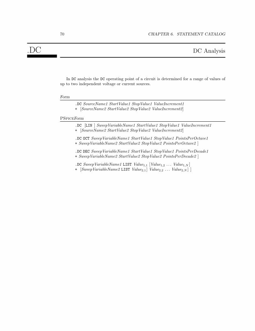
70 CHAPTER 6. STATEMENT CATALOG
.DC DC Analysis
In DC analysis the DC operating point of a circuit is determined for a range of values ofup to two independent voltage or current sources.
Form
.DC SourceName1 StartValue1 StopValue1 ValueIncrement1+ [SourceName2 StartValue2 StopValue2 ValueIncrement2]
PSpiceForm
.DC [LIN ] SweepVariableName1 StartValue1 StopValue1 ValueIncrement1+ [SourceName2 StartValue2 StopValue2 ValueIncrement2]
.DC OCT SweepVariableName1 StartValue1 StopValue1 PointsPerOctave1+ SweepVariableName2 StartValue2 StopValue2 PointsPerOctave2 ]
.DC DEC SweepVariableName1 StartValue1 StopValue1 PointsPerDecade1+ SweepVariableName2 StartValue2 StopValue2 PointsPerDecade2 ]
.DC SweepVariableName1 LIST Value1,1 [Value1,2 . . . Value1,N ]+ [SweepVariableName2 LIST Value2,1 ] Value2,2 . . . Value2,N ] ]
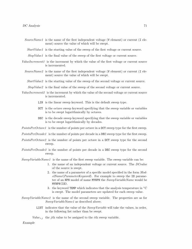
DC Analysis 71
SourceName1 is the name of the first independent voltage (V element) or current (I ele-ment) source the value of which will be swept.
StartValue1 is the starting value of the sweep of the first voltage or current source.
StopValue1 is the final value of the sweep of the first voltage or current source.
ValueIncrement1 is the increment by which the value of the first voltage or current sourceis incremented.
SourceName2 is the name of the first independent voltage (V element) or current (I ele-ment) source the value of which will be swept.
StartValue2 is the starting value of the sweep of the second voltage or current source.
StopValue2 is the final value of the sweep of the second voltage or current source.
ValueIncrement2 is the increment by which the value of the second voltage or current sourceis incremented.
LIN is the linear sweep keyword. This is the default sweep type.
OCT is the octave sweep keyword specifying that the sweep variable or variablesis to be swept logarithmically by octaves.
DEC is the decade sweep keyword specifying that the sweep variable or variablesis to be swept logarithmically by decades.
PointsPerOctave1 is the number of points per octave in a OCT sweep type for the first sweep.
PointsPerDecade1 is the number of points per decade in a DEC sweep type for the first sweep.
PointsPerOctave2 is the number of points per octave in a OCT sweep type for the secondsweep.
PointsPerDecade2 is the number of points per decade in a DEC sweep type for the secondsweep.
SweepVariableName1 is the name of the first sweep variable. The sweep variable can be:1. the name of an independent voltage or current source. The DCvalue
of the source is swept.2. the name of a parameter of a specific model specified in the form Mod-
elName(ParameterKeyword). For example to sweep the IS parame-ter of an NPN model of name MYNPN the SweepVariableName would beMYNPN(IS).
3. the keyword TEMP which indicates that the analysis temperature in Cis swept. The model parameters are updated for each sweep value.
SweepVariableName2 is the name of the second sweep variable. The properties are as forSweepVariableName1 as described above.
LIST indicates that the value of the SweepVariable will take the values, in order,in the following list rather than be swept.
Value i,j the jth value to be assigned to the ith sweep variable.
Example
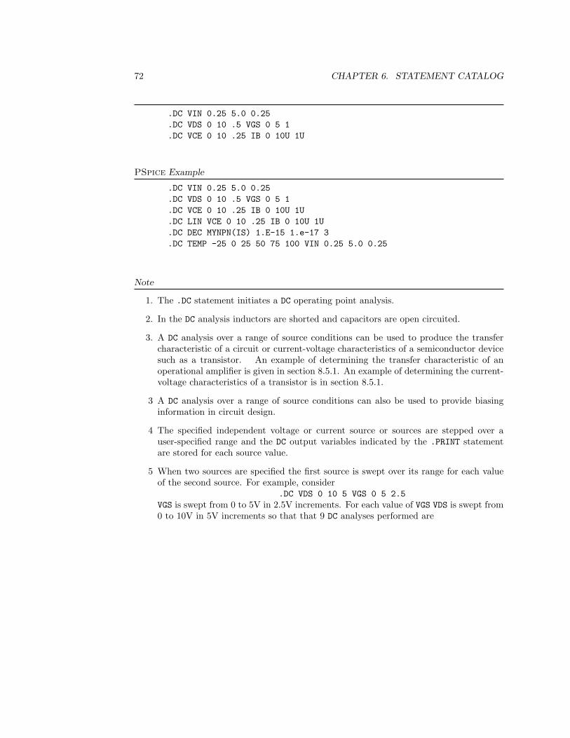
72 CHAPTER 6. STATEMENT CATALOG
.DC VIN 0.25 5.0 0.25
.DC VDS 0 10 .5 VGS 0 5 1
.DC VCE 0 10 .25 IB 0 10U 1U
PSpice Example
.DC VIN 0.25 5.0 0.25
.DC VDS 0 10 .5 VGS 0 5 1
.DC VCE 0 10 .25 IB 0 10U 1U
.DC LIN VCE 0 10 .25 IB 0 10U 1U
.DC DEC MYNPN(IS) 1.E-15 1.e-17 3
.DC TEMP -25 0 25 50 75 100 VIN 0.25 5.0 0.25
Note
1. The .DC statement initiates a DC operating point analysis.
2. In the DC analysis inductors are shorted and capacitors are open circuited.
3. A DC analysis over a range of source conditions can be used to produce the transfercharacteristic of a circuit or current-voltage characteristics of a semiconductor devicesuch as a transistor. An example of determining the transfer characteristic of anoperational amplifier is given in section 8.5.1. An example of determining the current-voltage characteristics of a transistor is in section 8.5.1.
3 A DC analysis over a range of source conditions can also be used to provide biasinginformation in circuit design.
4 The specified independent voltage or current source or sources are stepped over auser-specified range and the DC output variables indicated by the .PRINT statementare stored for each source value.
5 When two sources are specified the first source is swept over its range for each valueof the second source. For example, consider
.DC VDS 0 10 5 VGS 0 5 2.5VGS is swept from 0 to 5V in 2.5V increments. For each value of VGS VDS is swept from0 to 10V in 5V increments so that that 9 DC analyses performed are
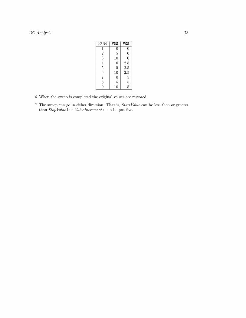
DC Analysis 73
RUN VDS VGS1 0 02 5 03 10 04 0 2.55 5 2.56 10 2.57 0 58 5 59 10 5
6 When the sweep is completed the original values are restored.
7 The sweep can go in either direction. That is, StartValue can be less than or greaterthan StopValue but ValueIncrement must be positive.
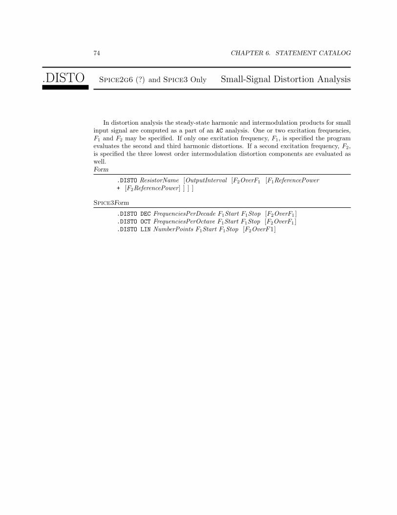
74 CHAPTER 6. STATEMENT CATALOG
.DISTO Spice2g6 (?) and Spice3 Only Small-Signal Distortion Analysis
In distortion analysis the steady-state harmonic and intermodulation products for smallinput signal are computed as a part of an AC analysis. One or two excitation frequencies,F1 and F2 may be specified. If only one excitation frequency, F1, is specified the programevaluates the second and third harmonic distortions. If a second excitation frequency, F2,is specified the three lowest order intermodulation distortion components are evaluated aswell.Form
.DISTO ResistorName [OutputInterval [F2OverF1 [F1ReferencePower+ [F2ReferencePower] ] ] ]
Spice3Form
.DISTO DEC FrequenciesPerDecade F1Start F1Stop [F2OverF1 ]
.DISTO OCT FrequenciesPerOctave F1Start F1Stop [F2OverF1 ]
.DISTO LIN NumberPoints F1Start F1Stop [F2OverF1]
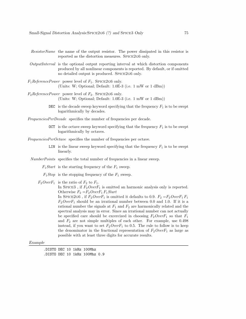
Small-Signal Distortion Analysis:Spice2g6 (?) and Spice3 Only 75
ResistorName the name of the output resistor. The power dissipated in this resistor isreported as the distortion measures. Spice2g6 only.
OutputInterval is the optional output reporting interval at which distortion componentsproduced by all nonlinear components is reported. By default, or if omittedno detailed output is produced. Spice2g6 only.
F1ReferencePower power level of F1. Spice2g6 only.(Units: W; Optional; Default: 1.0E-3 (i.e. 1 mW or 1 dBm))
F2ReferencePower power level of F2. Spice2g6 only.(Units: W; Optional; Default: 1.0E-3 (i.e. 1 mW or 1 dBm))
DEC is the decade sweep keyword specifying that the frequency F1 is to be sweptlogarithmically by decades.
FrequenciesPerDecade specifies the number of frequencies per decade.
OCT is the octave sweep keyword specifying that the frequency F1 is to be sweptlogarithmically by octaves.
FrequenciesPerOctave specifies the number of frequencies per octave.
LIN is the linear sweep keyword specifying that the frequency F1 is to be sweptlinearly.
NumberPoints specifies the total number of frequencies in a linear sweep.
F1Start is the starting frequency of the F1 sweep.
F1Stop is the stopping frequency of the F1 sweep.
F2OverF1 is the ratio of F2 to F1.In Spice3 , if F2OverF1 is omitted an harmonic analysis only is reported.Otherwise F2 =F2OverF1 F1StartIn Spice2g6 , if F2OverF1 is omitted it defaults to 0.9. F2 =F2OverF1 F1
F2OverF1 should be an irrational number between 0.0 and 1.0. If it is arational number the signals at F1 and F2 are harmonically related and thespectral analysis may in error. Since an irrational number can not actuallybe specified care should be excercized in choosing F2OverF1 so that F1
and F2 are not simple multiples of each other. For example, use 0.498instead, if you want to set F2OverF1 to 0.5. The rule to follow is to keepthe denominator in the fractional representation of F2OverF1 as large aspossible with at least three digits for accurate results.
Example
.DISTO DEC 10 1kHz 100Mhz
.DISTO DEC 10 1kHz 100Mhz 0.9
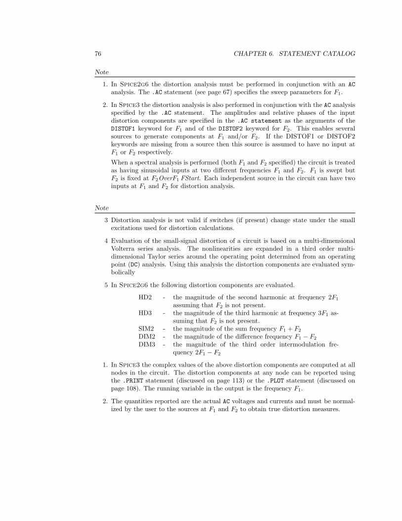
76 CHAPTER 6. STATEMENT CATALOG
Note
1. In Spice2g6 the distortion analysis must be performed in conjunction with an ACanalysis. The .AC statement (see page 67) specifies the sweep parameters for F1.
2. In Spice3 the distortion analysis is also performed in conjunction with the AC analysisspecified by the .AC statement. The amplitudes and relative phases of the inputdistortion components are specified in the .AC statement as the arguments of theDISTOF1 keyword for F1 and of the DISTOF2 keyword for F2. This enables severalsources to generate components at F1 and/or F2. If the DISTOF1 or DISTOF2keywords are missing from a source then this source is assumed to have no input atF1 or F2 respectively.
When a spectral analysis is performed (both F1 and F2 specified) the circuit is treatedas having sinusoidal inputs at two different frequencies F1 and F2. F1 is swept butF2 is fixed at F2OverF1 FStart. Each independent source in the circuit can have twoinputs at F1 and F2 for distortion analysis.
Note
3 Distortion analysis is not valid if switches (if present) change state under the smallexcitations used for distortion calculations.
4 Evaluation of the small-signal distortion of a circuit is based on a multi-dimensionalVolterra series analysis. The nonlinearities are expanded in a third order multi-dimensional Taylor series around the operating point determined from an operatingpoint (DC) analysis. Using this analysis the distortion components are evaluated sym-bolically
5 In Spice2g6 the following distortion components are evaluated.
HD2 - the magnitude of the second harmonic at frequency 2F1
assuming that F2 is not present.HD3 - the magnitude of the third harmonic at frequency 3F1 as-
suming that F2 is not present.SIM2 - the magnitude of the sum frequency F1 + F2
DIM2 - the magnitude of the difference frequency F1 − F2
DIM3 - the magnitude of the third order intermodulation fre-quency 2F1 − F2
1. In Spice3 the complex values of the above distortion components are computed at allnodes in the circuit. The distortion components at any node can be reported usingthe .PRINT statement (discussed on page 113) or the .PLOT statement (discussed onpage 108). The running variable in the output is the frequency F1.
2. The quantities reported are the actual AC voltages and currents and must be normal-ized by the user to the sources at F1 and F2 to obtain true distortion measures.
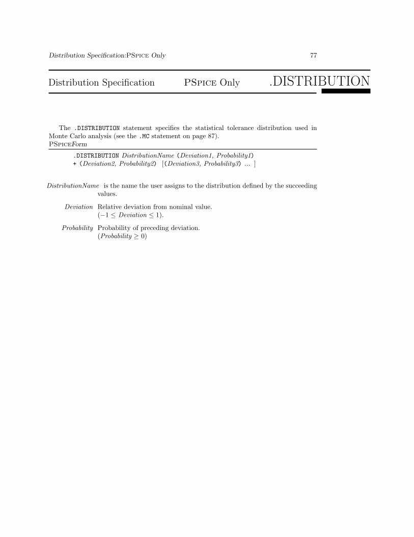
Distribution Specification:PSpice Only 77
Distribution Specification PSpice Only .DISTRIBUTION
The .DISTRIBUTION statement specifies the statistical tolerance distribution used inMonte Carlo analysis (see the .MC statement on page 87).PSpiceForm
.DISTRIBUTION DistributionName (Deviation1, Probability1)+ (Deviation2, Probability2) [(Deviation3, Probability3) ... ]
DistributionName is the name the user assigns to the distribution defined by the succeedingvalues.
Deviation Relative deviation from nominal value.(−1 ≤ Deviation ≤ 1).
Probability Probability of preceding deviation.(Probability ≥ 0)

78 CHAPTER 6. STATEMENT CATALOG
.DISTRIBUTION
Note
1. Parentheses, ‘(’ and ‘)’, and commas, ‘,’, in the NETLIST are ignored and are generallyused to make the NETLIST more readable.
2. The pairs of values (Deviation, Probability) define a piecewise linear probability distri-bution curve used in calculating the random numbers used in Monte Carlo analysis.
3. The Deviations must be in ascending order:Deviation1 < Deviation2 < Deviation3 < . . .
4. 100 (Deviation, Probability) pairs can be specified.

End Statement 79
End Statement .END
This statement indicates the end of the NETLIST of a circuit. While it is often insertedautomatically by most Spice simulators when the last statement of the NETLIST is readand it is not .END its usage is recommended as several circuits in one file are supported bysome versions of Spice including PSpice.Form
.END
80 CHAPTER 6. STATEMENT CATALOG
.ENDS End Subcircuit Statement
The end subcircuit statement indicates the end of a subcircuit definition.Form
.ENDS [SubcircuitName]
SubcircuitName Indicates which subcircuit is being terminated. If omitted, all subcircuitsbeing defined are terminated. Its use is required when nested subcircuitdefinitions are being made. It is good practise to use the full form of.ENDS.
Example
.ENDS NAND GATE
Note
1. See the definition of .SUBCKT on page 128.
Fourier Analysis 81
Fourier Analysis .FOUR
The Fourier analysis statement initiates a Fourier analysis of the results of a transientanalysis.Form
.FOUR Frequency OutputSpecification [OutputSpecification . . . ]
Frequency specifies the fundamental frequency of the transient waveform to be ana-lyzed. It is used to determine the period of the waveform.
OutputSpecification specifies the quantity to be reported as the result of the Fourier Analysis.It has the same format as the OutputSpecification in a .PRINT statement(see page 113).
Example
.FOUR 1M V(10,2) V(5) I(VLOAD)
Note
1. Fourier analysis uses the transient output waveform in the time interval from TSTOP−Tto TSTOP. T is the period of the Frequency parameter (T = 1/Frequency) specified inthe .FOUR statement. TSTOP is the final transient analysis time specified in the .TRANstatement (which is described on page 135.
2. Unlike most other analyses, a .PRINT, .PROBE or .PLOT statement is not required forthe data to be reported.
82 CHAPTER 6. STATEMENT CATALOG
.FUNC PSpice92 Only Function Definition
In this statement commonly used expressions can be defined as more convenient func-tions.PSpice92Form
.FUNC FunctionName( [Argument1, Argument2, . . . Argument10] ] ] ) = Function-Declaration
FunctionName is the name of the function being defined. It must begin with an alphabeticcharacter (A-Z).
Argument1 is a function argument. There can be from 0 to 10 arguments.
FunctionDeclaration can be any regular algebraic expression (see section ?? on page ??)and can use previously defined functions and the Laplace variable s. Theexpression delimiters and need not be used. The FunctionDeclaration isautomatically enclosed within the expression delimiters and . The func-tion declaration plus the two delimiters must be no more than 80 characters(one line) long.
Example
.FUNC
Note
1. The names of predefined functions must be avoided. The predefined functions arelisted in section ?? on page ??.
2. Functions are treated as macros in the C programming language. when user definedfunctions are invoked a textual expansion is performed and the resultant expansion isevaluated as a regular expression. The FunctionDeclaration before and after expansionis enclosed within expression delimiters and . This defines how nested functionsare treated.
3. It is faster to use predefined functions if available. Predefined functions also test thevalidity of the arguments and evaluate the correct as asymptotic behavior.
Initial Conditions 83
Initial Conditions .IC
The .IC statement is used to set initial conditions for transient analysis. It has no effecton other types of analyses.Form
.IC V(NodeName1)=Voltage1 [V(NodeName2) =Voltage2 . . . ]
V is the keyword specifying a node voltage
NodeName is the name of a node. Note that in Spice2g6 and Spice3 NodeName mustbe an integer.
Voltage is a numeric value.
Example
.IC V(11)=4.9 V(2)=2.5
Note
1. Initial conditions can be specified for the following elements: B (MESFET), C (capac-itor), D (diode), Q (BJT), M (MOSFET) and J (JFET)
2. The .IC statement has two different effects depending on whether the UIC (use initialconditions) keyword is present on the .TRAN statement.
(a) If the UIC keyword is specified in the .TRAN statement:The initial conditions specified in the .IC statement are used to establish theinitial conditions. Initial conditions specified for individual elements using the ICparameter on the element line will always have precedence over those specified ina .IC statement.No DC analysis is performed prior to a transient analysis. Thus it is important toestablish the initial conditions at all nodes using the .IC statement or using theIC element parameter.
(b) If the UIC keyword is not specified in the .TRAN statement:A DC analysis is performed prior to a transient analysis. During the DC analysisthe node voltages indicated in the .IC statement are held constant at the initialcondition values. During transient analysis the nodes are not constrained to theinitial condition values.

84 CHAPTER 6. STATEMENT CATALOG
.INC PSpice Only Include Statement
Form
.INC FileName
Filename is the name of the file which is to be included.
Note
1. The contents of Filename are read as if it were part of the original file.
2. Libraries could be included using the .INC statement or by the .LIB statement dis-cussed on page 85. The difference is that the .INC statement includes the contentsof the library file (except for comments) in internal data structures. However a .LIBstatement causes the library file to be scanned and an index constructed for model(.MODEL) and subcircuit (.SUBCKT) statements. The models subcircuits in the libraryfile are included in internal data structures if they are referred to. Thus the use of.LIB statements is a much more efficient way of using library files leading to both asmaller program and faster library access, especially for large libraries. Library filescan only contain models and subcircuits so that the type of files that can be incor-porated using a .LIB statement is more restricted than the type of file that can beincorporated using a .INC statement.

Library Statement:PSpice Only 85
Library Statement PSpice Only .LIB
The .LIB statement is an efficient way to include .MODEL statements and subcircuits.Form
.LIB [FileName ]
Filename is the name of the library file. (Optional; Default: NOM.LIB)
Note
86 CHAPTER 6. STATEMENT CATALOG
1. The library file can only contain a restricted set of Spice statements. It must containonly .MODEL statements, subcircuit definitions (between .SUBCKT and .ENDS state-ments), and .LIB statements.
2. The library file Filename is searched in the current directory and then in a list of di-rectories specified by the environment variable PSPICELIB (for compatibility purposesthe environment variable PSPICELIB is also supported).
3. If the DOS operating system is being used the library environment specification hasthe form
SET PSPICELIB = Directory1 [; Directory2 . . . ]
The environment variable may be set in the AUTOEXEC.BAT file in the root DOS direc-tory or before PSpice is evoked. For example:
SET PSPICELIB = C:\SPICE\MY LIB;D:\SPICE\TI LIB
4. If the UNIX operating system is being used the library environment specification hasthe form
setenv PSPICELIB = Directory1 [; Directory2 . . . ]
For example:
setenv PSPICELIB = /SPICE/MY LIB; /SPICE/TI LIB
5. Libraries could be included using the .INC statement or by the .LIB statement. Thedifference is that the .INC statement includes the contents of the library file (exceptfor comments) in internal data structures. However a .LIB statement causes the li-brary file to be scanned and an index constructed of model (.MODEL) and subcircuit(.SUBCKT) statements. The models subcircuits in the library file are included in inter-nal data structures only if they are referred to. Thus the use of .LIB statements is amuch more efficient way of using library files leading to both a smaller program andfaster library access, especially for large libraries.

Monte Carlo Analysis:PSpice Only 87
Monte Carlo Analysis PSpice Only .MC
The Monte Carlo analysis is a statistical analysis of the circuit causing the circuit to beanalyzed many times with a random change of model parameters (parameters in a .MODELstatement).PSpiceForm
.MC NumberOfRuns AnalysisType OutputSpecification OutputFunction [LIST]+ [OUTPUT( OutputSampleType )]
PSpice92Form
.MC NumberOfRuns AnalysisType OutputSpecification OutputFunction [LIST]+ [OUTPUT( OutputSampleType )] [RANGE(LowValue, HighValue)]+ [SEED=SeedValue]
88 CHAPTER 6. STATEMENT CATALOG
NumberOfRuns is the total number of runs to do. This number includes the initial nominalrun.
AnalysisType is the type of analysis to be performed in the Monte Carlo runs after theinitial nominal run (using the nominal values of model parameters). Allanalyses specified in the NETLIST are performed in the nominal run. TheAnalysisType must be one of the following:
DC is a keyword indicating that the DC analysis as specified bythe .DC statement is repeated. The sweep variable usedin analyzing the output OutputSpecification is the value ofthe independent voltage or current source specified in the.DC statement (as discussed on page 70).
AC is a keyword indicating that the AC small-signal analysisas specified by the .AC statement is repeated. The sweepvariable used in analyzing the output OutputSpecificationis frequency.
TRAN is a keyword indicating that the transient analysis as spec-ified by the .TRAN statement is repeated. The sweep vari-able used in analyzing the output OutputSpecification istime.
OutputSpecification specifies the quantity to be reported as the result of the Monte CarloAnalysis. It has the same format as the OutputSpecification in a .PRINTstatement (see page 113). The result is the value of the OutputSpecificationwith respect to a sweep for DC and AC analysis, and as a waveform for TRANanalysis.
OutputFunction indicates the function to be performed on the output indicated by Out-putSpecification to reduce the sweep or waveform at each run to a singlenumeric value. The OutputSpecification must be one of the followingkeywords:
YMAX which produces the greatest deviation of the sweep or wave-form from the nominal run.
MAX which results in the maximum value in each sweep or wave-form.
MIN which results in the minimum value in each sweep or wave-form.
RISE EDGE(Value) which reports as the result the first run when the wave-form crosses above the threshold Value. The algorithmused requires that one point in the waveform be belowValue and the succeeding point be above Value.
FALL EDGE(Value) which reports as the result the first run when the wave-form crosses below the threshold Value. The algorithmused requires that one point in the waveform be aboveValue and the succeeding point be below Value.
LIST is an optional keyword that results in the model parameter values that arestatistically varied being printed out prior to each run. If it is omitted thenthe statistically generated model parameter values are not produced priorto each run.
OUTPUT is an optional keyword indicating the type of output to be produced by runsafter the initial nominal run. The output produced for each run sampled isdetermined by the .PLOT, .PRINT and .PROBE statements in the NETLIST.If this keyword is missing output is produced only for the nominal run.
OutputSampleType indicates the method by which runs are selected for output reporting.The output produced for each run selected is determined by the .PLOT,.PRINT and .PROBE statements in the NETLIST. OutputSampleType mustbe one of the following:
ALL indicates that the output is to be produced for all runs.
FIRST Nruns indicates that the output is to be produced only for thefirst Nruns runs.
EVERY NthRun indicates that the output is to be produced for NthRunthrun.
RUNS Run1 [Run2 ... [Run25 ] ] indicates that the output is to be pro-duced for the indicated runs. Up to 25 runs can be indi-cated.
RANGE is an optional range indicating the range of the sweep variable over whichOutputFunction is to be performed. If this keyword is missing, output isproduced but the range is not restricted. The range of the sweep variableto be considered is from LowValue to HighValue inclusive.
LowValue is the low end of the sweep variable to be considered in evaluating Output-Function.
HighValue is the low end of the sweep variable to be considered in evaluating Output-Function.
SEED is the keyword for the seed of the random number generator used in MonteCarlo Analysis
SeedValue is the value of the seed used in the random number generator used toselect sample runs at random. (Optional; Default: 17,533; 1 ≤ SeedValue≤32, 767)
Note
Monte Carlo Analysis:PSpice Only 89
1. A typical use of Monte Carlo analysis is to predict yield of a circuit by examining theeffect of process variations such as length and width of transistors.
2. A .TEMP statement also can result in multiple circuit simulations as the temperatureis varied. In conjunction with a .MC statement a Monte Carlo analysis is performedfor each temperature before the temperature is updated in a temperature sweep.
3. Only model parameters (parameters in a .MODEL statement) are varied.
4. If the AnalysisType is DC only one independent voltage or current source can be spec-ified in the .DC statement (discussed on page 70).
5. The random number generator is the subtractive method generator described by Knuth[28, p. 171].
6. The initial run uses the nominal parameter values given in the NETLIST. Subsequentruns statistically vary model parameters indicated as having either lot LOT or deviceDEV tolerances. These tolerances are specified in a .MODEL statement (see page 90).
MethodThe initial Run of a Monte Carlo Analysis uses the nominal values of the model parameterspossibly updated to their new values if the analysis temperature is different from the thenominal temperature in effect when the .MODEL statement was read. The nominal valuesof the model parameters as well as their tolerances and type of statistical distribution arespecified in a .MODEL statement (see page 90). If X(T ) is the value of the model parameterat temperature T , r is a random number between −1 and +1 inclusive, and XT is thetolerance of X(TNOM) is the nominal temperature, the value of X to be used in Monte Carloanalysis is
X ′(T ) = X(T )(1 + rXT ) (6.1)
The random number r has a statistical distribution which has a type indicated in the.MODEL statement. The distribution type must be either one of the built-in distributionsor specified by the user in a .DISTRIBUTION statement (see page 77). The tolerance isspecified immediately following the distribution in a .MODEL statement. Specification ofthe distribution type and tolerance assignment are described on page 92.

90 CHAPTER 6. STATEMENT CATALOG
.MODEL Model Statement
Model statements specify the parameters of elements that either are too numerous toput on the element line or are common to many elements.
Form
.MODEL ModelName ModelType (Keyword=Value ... )
PSpiceForm
.MODEL ModelName ModelType (Keyword=Value [ToleranceSpecification] . . . )
ModelName is the name of the model specified by the user.
ModelType is the model type which is specific to particular elements. The model typesare given in the table below.
ToleranceSpecification is the specification of the statistical distribution and tolerance of aparameter. This is used in a Monte Carlo simulation to assign randomvariations to the model parameter. ToleranceSpecification is discussed onpage 92.
Keyword is the name of the model parameter which is discussed on the pages referredto below.
Value is the numeric value of the model parameter.
Example
.MODEL MOSFET1 MOS (LEVEL=2 VTO=-0.76 GAMMA=0.6 CGSO=3.35E-10)

Model Statement 91
.MODEL
MODEL SPICE ELEMENT DESCRIPTION PAGETYPE VERSION— NAME
PASSIVE DEVICE MODELSRES R resistor model 284, 284CAP C capacitor model 183, 184IND PSpice L inductor model 230
SEMICONDUCTOR DEVICE MODELSD D diode model 187NPN Q NPN bjt model 274PNP Q PNP bjt model 274LPNP PSpice Q Lateral PNP bjt model 274NJF J N-channel junction FET (JFET) 213PJF J P-channel junction FET (JFET) 213GASFET PSpice B N-channel GaAs MESFET 313, 145NMF Spice3 B N-channel GaAs MESFET ??PMF Spice3 B P-channel GaAs MESFET ??NMOS M N-channel MOSFET 233PMOS M P-channel MOSFET 233SWMODEL Spice3 ??URC Spice3 T Lossy RC transmission line 292
MISCELLANEOUS DEVICE MODELSCORE PSpice K nonlinear, transformer (magnetic core) 224VSWITCH PSpice S voltage switch 287ISWITCH PSpice W current switch 307SW Spice3 ??CSW Spice3 ??
DISTRIBUTED DEVICE MODELSURC Uniform Distributed RC model 292

92 CHAPTER 6. STATEMENT CATALOG
.MODELMODEL SPICE ELEMENT DESCRIPTION PAGETYPE VERSION NAME
DIGITAL INTERFACE AND DIGITAL DEVICE MODELSDINPUT PSpice N digital input model 268DOUTPUT PSpice O digital output model 271UIO PSpice U digital I/O model ??UGATE PSpice U standard gate ??UTGATE PSpice U tri-state gate ??UEFF PSpice U edge-triggered flip-flop ??UGFF PSpice U gated flip-flop ??UWDTH PSpice U pulse width checker ??USUHD PSpice U setup and hold checker ??UDLY PSpice U digital delay line ??UADC PSpice U multi-bit analog-to-digital converter ??UDAC PSpice U multi-bit digital-to-analog converter ??
Virtually all of the device model parameters have default values which generally result intypical operation.
Tolerance and Distribution AssignmentImmediately following the specification of a model parameter a statistical distributionTolerance
Specification and tolerance can be assigned. These are used in conjunction with Monte Carlo analysiswhich is controlled by the .MC statement described on page 87 The Monte Carlo analysisis a statistical analysis of the circuit causing the circuit to be analyzed many times with arandom change of certain model parameters). The form of the tolerance and distributionassignment is
DEV [/DeviceTrackingIndex] [/DistributionType] Tolerance [%]+ LOT [/LotTrackingIndex] [/DistributionType] Tolerance [%]

Model Statement 93
DEV is the keyword for the device tolerance specification.
DeviceTrackingIndex specifies which random number to use. It must be one of 1, 2, ... 10.Two parameters with the same DeviceTrackingIndex are correlated. Con-versely if two parameters have different DeviceTrackingIndex then they areuncorrelated.LotTrackingIndex and DeviceTrackingIndex refer to different random num-bers and so choosing the same LotTrackingIndex and DeviceTrackingIndexdoes not correlate the LOT and DEV distributions.(Units: none; Optional; Default: 1)
DistributionType is the type of the statistical distribution used in generating random num-bers. There are two predefined distribution types and a user specified dis-tribution type can be used. The allowable types are:
UNIFORM specifies a uniform distribution of random numbers be-tween -1 and +1.
GAUSS specifies a Gaussian distribution of random numbers be-tween ±4σ. In this case Tolerance specifies σ.
DistributionName is the name of a user specified distribution specified in a.DISTRIBUTION statement (see page 77).
LotTolerance is the lot tolerance specification. It may be specified as an absolute quantityor as a percentage if followed by %. It is converted to a fraction of thenominal value. The magnitude of the fractional value must be ≤ 1.
LOT is the keyword for the lot tolerance specification.
LotTrackingIndex specifies which random number to use. It must be one of 1, 2, ... 10. Twoparameters with the same LotTrackingIndex are correlated. Conversely twoparameters have different LotTrackingIndex’s then they are uncorrelated.LotTrackingIndex and DeviceTrackingIndex refer to different random num-bers and so choosing the same LotTrackingIndex and DeviceTrackingIndexdoes not correlate the LOT and DEV distributions.(Units: none; Optional; Default: 1)
DeviceTolerance is the device tolerance specification. It may be specified as an absolutequantity or as a percentage if followed by %. It is converted to a fractionof the nominal value. The magnitude of the fractional value must be ≤ 1.
Example
.MODEL
94 CHAPTER 6. STATEMENT CATALOG
Note
1. Both lot (LOT) and device (DEV) tolerances can be specified separately. Lot and devicetolerances combine for the purposes of determining the total tolerance of a modelparameter. The sum of device and lot tolerances must be less than the nominal modelparameter value (i.e. is less than 100%).
2. A total of 20 random number are generated internally. Of these 10 are for lot toleranc-ing and 10 are for device tolerancing. Parameters with the same lot tolerance index(LotToleranceIndex) use the same random number to generate statistical variationsand so are fully correlated. Similarly parameters with the same device tolerance index(DeviceToleranceIndex) use the same random number. However the random numberfor a lot and that for a device are always uncorrelated. If X(T ) is the value of amodel parameter at temperature T , RLOT(LotToleranceIndex ) is random number forlot variations and RDEV(DeviceToleranceIndex ) is random number for device varia-tions, XLOT is the fractional lot tolerance XDEV is the fractional device tolerance, thevalue used in a Monte Carlo simulation is
X ′(T ) = X(T ) (1 + RLOT(LotTrackingIndex )XLOT + RDEV(DeviceTrackingIndex )XDEV)(6.2)

Node Voltage Initialization 95
Node Voltage Initialization .NODESET
Form
.NODESET V(NodeName)=Voltage [V(NodeName)=Voltage . . . ]
V is the keyword specifying a node voltage
NodeName is the name of a node. Note that in Spice2g6 and Spice3 NodeName mustbe an integer.
Example
.NODESET V(11)=4.9 V(2)=2.5
Note
1. This statement can be used if convergence problems are encountered in a DC analysis.For most circuits Spice will be able to determine the DC voltage or initial transientsolution.
2. The statement can be used with astable circuits such as multivibrators and flip flopsto ensure that these circuits are initialized in a particular state.

96 CHAPTER 6. STATEMENT CATALOG
.NOISE Small-Signal Noise Analysis
In noise analysis the noise generated by active devices and resistors is evaluated.Form
.NOISE OutputVoltageSpecification InputSourceName OutputInterval
Spice3Form
.NOISE OutputVoltageSpecification InputSourceName DEC+ FrequenciesPerDecade FStart FStop [OutputInterval ]
.NOISE OutputVoltageSpecification InputSourceName OCT+ FrequenciesPerOctave FStart FStop [OutputInterval ]
.NOISE OutputVoltageSpecification InputSourceName LIN+ NumberPoints FStart FStop OutputInterval
Small-Signal Noise Analysis 97
OutputVoltageSpecification is a specification of an output voltage which is to be the output ofthe noise analysis. It acts as a summing point for the noise contributions ofthe individual noise current generators. The noise voltage appearing at theoutput for each noise generator is summed in the RMS sense. Any voltagespecification may be used including the voltage at a node, e.g. using V(5),or the voltage between nodes, e.g. using V(5,3). The noise is reported inunits of V/
√Hz.
InputSourceName is the name of the independent voltage (V) or current (I) source that isto be the input reference source to which equivalent input noise is referred.The input source does not produce noise itself. If the input source is anindependent voltage source then the equivalent input noise is reported inunits of V/
√Hz. If the input source is an independent current source then
the equivalent input noise is reported in units of A/√
Hz.
OutputInterval is the optional output reporting interval at which the values of the noisecurrent generators internal to the elements of the circuit are reported. Thereport is produced every OutputInterval th frequency. If zero or omitted nodetailed output is produced.
DEC is the decade sweep keyword specifying that the noise analysis is to beevaluated at a number of frequency points. The frequency is swept loga-rithmically by decades.
FrequenciesPerDecade specifies the number of frequencies per decade.
OCT is the octave sweep keyword specifying that the noise analysis is to beevaluated at a number of frequency points. The frequency is swept loga-rithmically by octaves.
FrequenciesPerOctave specifies the number of frequencies per octave.
LIN is the linear frequency sweep keyword. At each frequency a noise analysisis performed.
NumberPoints specifies the total number of frequencies in a linear sweep.
FStart is the starting frequency of the sweep.
FStop is the stopping frequency of the sweep.
Example
.NOISE V(5) VIN DEC 10 1kHZ 100Mhz
.NOISE V(5,3) V1 OCT 8 1.0 1.0e6 1
Example

98 CHAPTER 6. STATEMENT CATALOG
.NOISE V(5) VIN
.NOISE V(5,3) I1
Note
1. In noise analysis the noise generated by active devices and resistors is evaluated as anoise spectral density. The densities are integrated over the the range of frequenciesto obtain a gross noise measure for the circuit (for the specified frequency range).The finer the frequency spacing the more accurate will be the noise analysis. Thenoise contributions of individual noise generators are summed at the node or branchspecified by OutputVoltageSpecification. The noise at this output port is reported aswell as the equivalent input noise (the output noise referred to the input) at the inputsource identified by InputSourceName.
2. Two types of output are produced by noise analysis:
(a) noise spectral density versus frequency, and
(b) total integrated noise over the specified frequency range.
3. In Spice3 the AC frequency sweep for noise analysis must be specified in the .NOISEstatement. In PSpice the frequency sweep specified in the .AC statement is used.
4. The noise table is produced while analysis is being performed. Noise reporting isproduced using the .PRINT and .PLOT statements.
5. Noise is generated by resistors and by semiconductor devices. Resistors generatethermal noise while the noise model of semiconductor devices includes thermal noise,shot noise and flicker noise. Noise models of individual elements are discussed in theelement catalog beginning on page 143.

Operating Point Analysis 99
Operating Point Analysis .OP
In the operating point analysis a DC analysis is performed to determine the DC voltagesand currents without performing any sweeps.Form
.OP
Note
1. The operating point analysis is performed by default prior to AC small-signal (.AC) andtransient (.TRAN) analyses to determine the operating point about which the circuitis linearized for AC analysis and as the initial starting point for transient analysis.
2. The (.OP) analysis is performed if no other analyses are specified.
3. The operating point analysis is performed with inductors shorted and capacitorsopened.
4. Following DC analysis the nonlinear devices are linearized to determine their AC small-signal models.
5. A .TRAN analysis performs its own DC analysis to determine the initial conditions (orbias point) for transient analysis ignoring the bias point determined in a .OP analysis.
100 CHAPTER 6. STATEMENT CATALOG
.OPTIONS Option Specification
The options specification provides the user control over the program and a way of settingdefaults for certain elements and analyses.Form
.OPTIONS [Keyword] ... [Keyword=Value] ...
Multiple keywords can be included in a single .OPTIONS statement and in any order.
Keywords:
ACCT Sets reporting of accounting and statistics. This option is a flag and doesnot have a value.(Default: not set)
ABSTOL=Value Sets the absolute current error tolerance.(Default: 1 pA (10−12))
BYPASS The bypass option.Spice3 only.
CHGTOL=Value Resets the charge tolerance of the program.(Units: C; Default: 10 fC 10−14)
CPTIME=Value Sets the maximum CPU-time.(Units: s; Default: ∞)Spice2g6 only.
DEFAD=Value Sets the default value of the MOS drain diffusion area (AD) used in the Melement (see page 231).(Units: m2 Default: 0)
DEFAS=Value Sets the default value of the MOS source diffusion area (AS) used in the Melement (see page 231).(Units: m2 Default: 0)
Option Specification 101
.OPTIONSDEFL=Value Sets the value of the MOS channel length (L) used in the M element (see
page 231).(Units: m; Default: 100µm (1E-4))
DEFW=Value Resets the value for MOS channel width (W) used in the M element (seepage 231).(Units: m; Default: 100 µm (1E-4))
EXPAND Reports in output logfile the devices and nodes created in subcircuit ex-pansions. This option is a flag and does not have a value.(Default: no expansion)PSpice only.
GMIN=Value Resets the value of the minimum conductance GMIN. The usage of GMIN iscontrolled by the code implementing individual elements. Generally is theminimum conductance between nodes. It is used to aid convergence.(Units: S; Default: 10−12 (1E-12))
ITL1=IntegerValue Sets the limit on the number of DC iterations.(Default: 100)
ITL2=IntegerValue Sets the DC transfer curve iteration limit.(Default: 50)
ITL3=IntegerValue Sets the minimum number of iterations used in transient analysis.(Default: 4)Spice2g6 only.
ITL4=IntegerValue Sets the maximum of transient iterations at each time point.(Default: 10)Spice2g6 only.
ITL5=IntegerValue Sets the transient analysis total iteration limit. If ITL5=0 this test isomitted. Used in transient analysis (.TRAN).PSpice only.(Default: 5000)
LIBRARY Reports in output logfile the statements and devices extracted from a li-brary file This option is a flag and does not have a value.(Default: no report)PSpice only.

102 CHAPTER 6. STATEMENT CATALOG
LIMPTS=Value Sets the maximum number of points that can be printed or plotted in a DC, AC or transient analysis.(Default: 201)Spice2g6 only.
LIMTIM=Value Sets the maximum CPU time for generating plots. Used only if the pro-gram was terminated because the time specified by the CPTIME option wasexceeded.(Units: s; Default: 10)Spice2g6 only.
Option Specification 103
.OPTIONSLIST Sets summary reporting of circuit elements in input NETLIST.
(Default: not set)
LVLCOD=IntegerValue Sets an internal option of the program when running on CDC com-puters. If LVLCOD=1 machine code for the matrix solution is generated.(Default: 2)Spice2g6 only.
LVLTIM=IntegerValue If LVLTIM=1 then iteration time step control is used. If LVLTIM=2then the time step indicated by the truncation error is used. If METHOD=GEARand MAXORD¿2 then LVLTIM is set to 2 by SPICE.(Default: 2)Spice2g6 only.
MAXORD=IntegerValue Sets the maximum order of the integration method if METHOD=GEAR(Default: 2; 2≤MAXORD≤6)Spice2g6 only.
METHOD=String Sets the numerical integration method to be used. If METHOD=GEAR thenGear’s method is used. If METHOD=TRAPEZOIDAL then the trapezoidal methodis used.(Default: TRAPEZOIDAL)Spice2g6 only.
NODE Sets reporting of the node table.(Default: not set)
NOECHO Suppresses listing of input file in output log file.(Default: input lines listed.)PSpice only.
[NOFREQ ] Number of frequency points to be used in simulation of distributed circuit.Must be a power of 2.(Default: 1024)
NOMOD Un-sets reporting of model parameters.(Default: set)
NOPAGE Un-sets page breaks in the output log file. Useful if the log file is to printedby a program which automatically paginates the output. This option is aflag and does not have a value.(Default: set)

104 CHAPTER 6. STATEMENT CATALOG
NUMDGT=IntegerValue Sets the number of significant digits used in printing values in theoutput log file.(Default: 4; 0 < IntegerValue ≤ 8)Spice2g6 and PSpice only.
Option Specification 105
.OPTIONSOPTS Sets reporting of the option values.
(Default: not set)
PIVREL=Value Sets the minimum acceptable pivot value used in partial pivoting in thesolution of the network equations (such as solving for the nodal voltagesvn in (4.1) on page 45). PIVREL is the minimum acceptable ratio of anacceptable pivot value to the largest column entry.(Default: 0.001)
PIVTOL=Value Sets the minimum value of a matrix element for it to be used as a pivot.(Default: 10−13)
RELTOL=Value Sets the relative error tolerance of voltages and currents.(Default: 0.001)
TNOM=Value Sets the nominal temperature. This is assumed to be the temperature atwhich the model parameters were measured. In some cases it is overwrittenby a temperature parameter in the .MODEL statement.(Units: C; Default: 27C (300K))
TRTOL=Value Sets the factor by which the approximated truncation error evaluated intransient analysis is scaled.(Default: 7)
VNTOL=Value Sets the absolute voltage error tolerance.(Units: V; Default: 1µV (1E-6))
106 CHAPTER 6. STATEMENT CATALOG
.PARAM PSpice92 Only Parameter Definition
This statement defines parameters that can be used in subsequent statements and ele-ment lines.PSpiceForm
.PARAM [ParameterName = NumericValue . . . ] [ParameterName = Expression . . . ]
ParameterName Name of a parameter with first character being alphabetic (a-z). If this isthe name of a previously defined parameter at the same level of subcircuitexpansion then the parameter value is changed. If the .PARAM statement isis in the top level circuit then the parameter value is global. If the .PARAMstatement is is in a subcircuit then the parameter value is local and canbe used at the current subcircuit expansion level or lower in the subcircuitexpansion hierarchy.
NumericValue is a numeric value which can be an integer or floating point number followedby optional scale factor and/or unit. (e.g. 1.E-9, 1N, 1NV and 1.E-9V areequivalent.)
Expression is a standard expression as described in the Algebraic Expressions sectionon page ??. Note that the expression must be enclosed in braces ( . . . ).
Example
.PARAM VDD = 10V, VSS = 0 VREF = 2.5
.PARAM VREF = VDD/2 .PARAM LENGTH = 1.10*L
Note

Parameter Definition:PSpice92 Only 107
1. Predefined parameters are supported and the user must avoid using these. Predefinedparameters:
Name Value DescriptionTEMP not supported Analysis temperature.
Reserved for future expansion
VT not supported Thermal voltage.Reserved for future expansion
2. In PSpice , in most places where a numeric value is required an expression (withinbraces . . . ) can be used instead. An expression can contain any support mathe-matical operation, constant numeric values or expressions. Exceptions are
• Polynomial coefficients.
• The values of the transmission line device parameters NL and F.
• The values of the piece-wise linear characteristic in the PWL form of the indepen-dent voltage (V) and current (I) sources.
and
• The values of the resistor device parameter TC.
• As node numbers.
• Values of most statements (such as .TEMP, .AC, .TRAN etc.)
Specifically included are
• The values of all other device parameters.
• The values in .IC and .NODESET statements.
• The values in .SUBCKT statements.
and
• The values of all model parameters. F.
3. Hierarchical usage of .PARAM statements in subcircuits is supported. The parametersdefined in a .PARAM statement are available in the subcircuit in which they are definedor in lower nested subcircuits. Thus parameters defined in a subcircuit are not availablehigher in the hierarchy. The same concept applies to values of a parameter changed ina subcircuit. Value changes are local and are available in the current subcircuit andlower nested subcircuits.
4. Libraries are searched for parameters not defined in the circuit NETLIST or in includedfiles. A .PARAM statement does not have to be within a subcircuit in a library.
108 CHAPTER 6. STATEMENT CATALOG
.PLOT Plot Specification
The plot specification controls the information that is plotted as the result of variousanalyses.Form
.PLOT TRAN OutputSpecification [PlotLimits]+ [OutputSpecification [PlotLimits] . . . ]
.PLOT AC OutputSpecification [PlotLimits]+ [OutputSpecification [PlotLimits] . . . ]
.PLOT DC OutputSpecification [PlotLimits]+ [OutputSpecification [PlotLimits] . . . ]
.PLOT NOISE NoiseOutputSpecification [(DistortionReportType)] [PlotLimits]+ [NoiseOutputSpecification [(DistortionReportType)] [PlotLimits]
.PLOT DISTO DistortionOutputSpecification [(DistortionReportType)] [PlotLimits]+ [DistortionOutputSpecification [(DistortionReportType) ] [PlotLimits ] . . . ][(DistortionReportType)] [PlotLimits]
PSpiceForm
.PLOT TRAN OutputSpecification [PlotLimits]+ [OutputSpecification [PlotLimits] . . . ]
.PLOT AC OutputSpecification [PlotLimits]+ [OutputSpecification [PlotLimits] . . . ]
.PLOT DC OutputSpecification [PlotLimits]+ [OutputSpecification [PlotLimits] . . . ]
.PLOT NOISE NoiseOutputSpecification [(DistortionReportType)] [PlotLimits]+ [NoiseOutputSpecification [(DistortionReportType)] [PlotLimits]
Plot Specification 109
TRAN is the keyword specifying that this .PLOT statement controls the reportingof results of a transient analysis initiated by the .TRAN statement.
AC is the keyword specifying that this .PLOT statement controls the reportingof results of a small-signal AC analysis initiated by the .AC statement.
DC is the keyword specifying that this .PLOT statement controls the reportingof results of a DC analysis initiated by the .DC statement.
NOISE is the keyword specifying that this .PLOT statement controls the reportingof results of a noise analysis initiated by the .NOISE statement.
DISTO is the keyword specifying that this .PLOT statement controls the reportingof results of a small-signal AC distortion analysis initiated by the .DISTOstatement.
OutputSpecification specifies the voltage or current to be plotted against the sweep variable.The sweep variable is dependent on the type of analysis.Many forms of OutputSpecification are supported by PSpice . Belowis a description of the basic forms that are supported both by Spice2g6and PSpice . A comprehensive description of OutputSpecification sup-ported by PSpice is given in the section on output specification on page116.
Voltages may be specified as an absolute voltage at a node: V(NodeName)or the voltage at one node with respect to that at another node, e.g.V(Node1Name,Node2Name).For the reporting of the results of an AC analysis the following outputs canbe specified by replacing the V as follows:
VR - real partVI - imaginary partVM - magnitudeVP - phaseVDB - 10 log(10 magnitude)
In AC analysis the default is VM for magnitude.
Currents are specified by referencing the name of the voltage source throughwhich the current is measured, e.g. I(VVoltageSourceName).

110 CHAPTER 6. STATEMENT CATALOG
For the reporting of the results of an AC analysis the following outputs canbe specified by replacing the I as follows:
IR - real partII - imaginary partIM - magnitudeIP - phaseIDB - 10 log(10 magnitude)
In AC analysis the default is IM for magnitude.
PlotLimits are optional and can be placed after any output specification. PlotLimitshas the form (LowerLimit,UpperLimit) . All quantities will be plottedusing the same PlotLimits. The default is to automatically scale the plotand perhaps use different scales for each of the quantities to be plotted.
NoiseOutputSpecification specifies the noise measure to be reported. The two options areONOISE which reports the output noise and INOISE which reports the equiv-alent input noise. See the .NOISE statement on page 96 for a detailedexplanation.

Plot Specification 111
It must be one of the following:ONOISE - magnitude of the output noiseDB(ONOISE) - output noise in dBINOISE - magnitude of the equivalent input noiseDB(INOISE) - equivalent input noise in dBGAIN - voltage gainDB(GAIN) - voltage gain in dB (= 20 log(GAIN)GT - transducer gainDB(GT) - transducer gain in dB (= 10 log(GT)NF - spot noise factorDB(NF) - spot noise figure (= 10 log(NF)SNR - output signal-to-noise ratioDB(SNR) - output signal-to-noise ratio in dB (= 20 log(SNR)TNOISE - output noise temperature.
SParameterOutputSpecification specifies the S-parameter output variables that are to beprinted. Each variable must have one of the following forms:
S(i,j) - Magnitude of Sij
SR(i,j) - Real part of Sij
SI(i,j) - Imaginary part of Sij
SP(i,j) - Phase of Sij in degreesSDB(i,j) - Magnitude of Sij in dB (= 20 log(S(i,j)))SG(i,j) - Group delay of Sij
The port numbers are i, j which are specified using the PNR keywor whenthe port (‘P’) element is specified.
DistortionOutputSpecification specifies the distortion component to be reported in a tabularformat of up to 8 columns plus an initial column with the sweep variable.The DistortionOutputSpecification is one of the following:
HD2 - the second harmonic distortionHD3 - the second harmonic distortionSIM2 - the sum frequency intermodulation componentDIM2 - the difference frequency intermodulation componentDIM3 - the third order intermodulation component
See the .DISTO statement on page 74 for a description of these distortioncomponents.
DistortionReportType specifies the format for reporting the distortion components. It mustbe one of the following:
R - real partI - imaginary partM - magnitudeP - phaseDB - 10 log(10 magnitude)
The default is M for magnitude.
Example
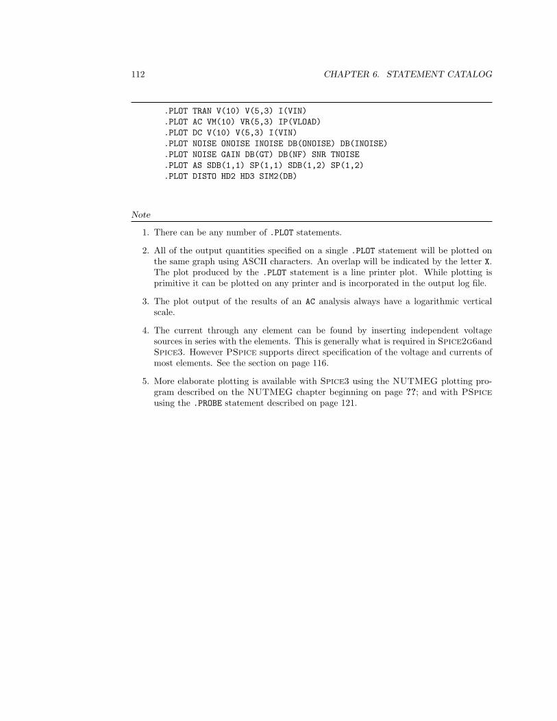
112 CHAPTER 6. STATEMENT CATALOG
.PLOT TRAN V(10) V(5,3) I(VIN)
.PLOT AC VM(10) VR(5,3) IP(VLOAD)
.PLOT DC V(10) V(5,3) I(VIN)
.PLOT NOISE ONOISE INOISE DB(ONOISE) DB(INOISE)
.PLOT NOISE GAIN DB(GT) DB(NF) SNR TNOISE
.PLOT AS SDB(1,1) SP(1,1) SDB(1,2) SP(1,2)
.PLOT DISTO HD2 HD3 SIM2(DB)
Note
1. There can be any number of .PLOT statements.
2. All of the output quantities specified on a single .PLOT statement will be plotted onthe same graph using ASCII characters. An overlap will be indicated by the letter X.The plot produced by the .PLOT statement is a line printer plot. While plotting isprimitive it can be plotted on any printer and is incorporated in the output log file.
3. The plot output of the results of an AC analysis always have a logarithmic verticalscale.
4. The current through any element can be found by inserting independent voltagesources in series with the elements. This is generally what is required in Spice2g6andSpice3. However PSpice supports direct specification of the voltage and currents ofmost elements. See the section on page 116.
5. More elaborate plotting is available with Spice3 using the NUTMEG plotting pro-gram described on the NUTMEG chapter beginning on page ??; and with PSpiceusing the .PROBE statement described on page 121.
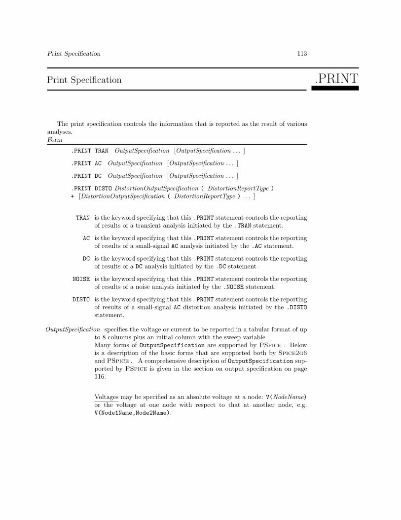
Print Specification 113
Print Specification .PRINT
The print specification controls the information that is reported as the result of variousanalyses.Form
.PRINT TRAN OutputSpecification [OutputSpecification . . . ]
.PRINT AC OutputSpecification [OutputSpecification . . . ]
.PRINT DC OutputSpecification [OutputSpecification . . . ]
.PRINT DISTO DistortionOutputSpecification ( DistortionReportType )+ [DistortionOutputSpecification ( DistortionReportType ) . . . ]
TRAN is the keyword specifying that this .PRINT statement controls the reportingof results of a transient analysis initiated by the .TRAN statement.
AC is the keyword specifying that this .PRINT statement controls the reportingof results of a small-signal AC analysis initiated by the .AC statement.
DC is the keyword specifying that this .PRINT statement controls the reportingof results of a DC analysis initiated by the .DC statement.
NOISE is the keyword specifying that this .PRINT statement controls the reportingof results of a noise analysis initiated by the .NOISE statement.
DISTO is the keyword specifying that this .PRINT statement controls the reportingof results of a small-signal AC distortion analysis initiated by the .DISTOstatement.
OutputSpecification specifies the voltage or current to be reported in a tabular format of upto 8 columns plus an initial column with the sweep variable.Many forms of OutputSpecification are supported by PSpice . Belowis a description of the basic forms that are supported both by Spice2g6and PSpice . A comprehensive description of OutputSpecification sup-ported by PSpice is given in the section on output specification on page116.
Voltages may be specified as an absolute voltage at a node: V(NodeName)or the voltage at one node with respect to that at another node, e.g.V(Node1Name,Node2Name).
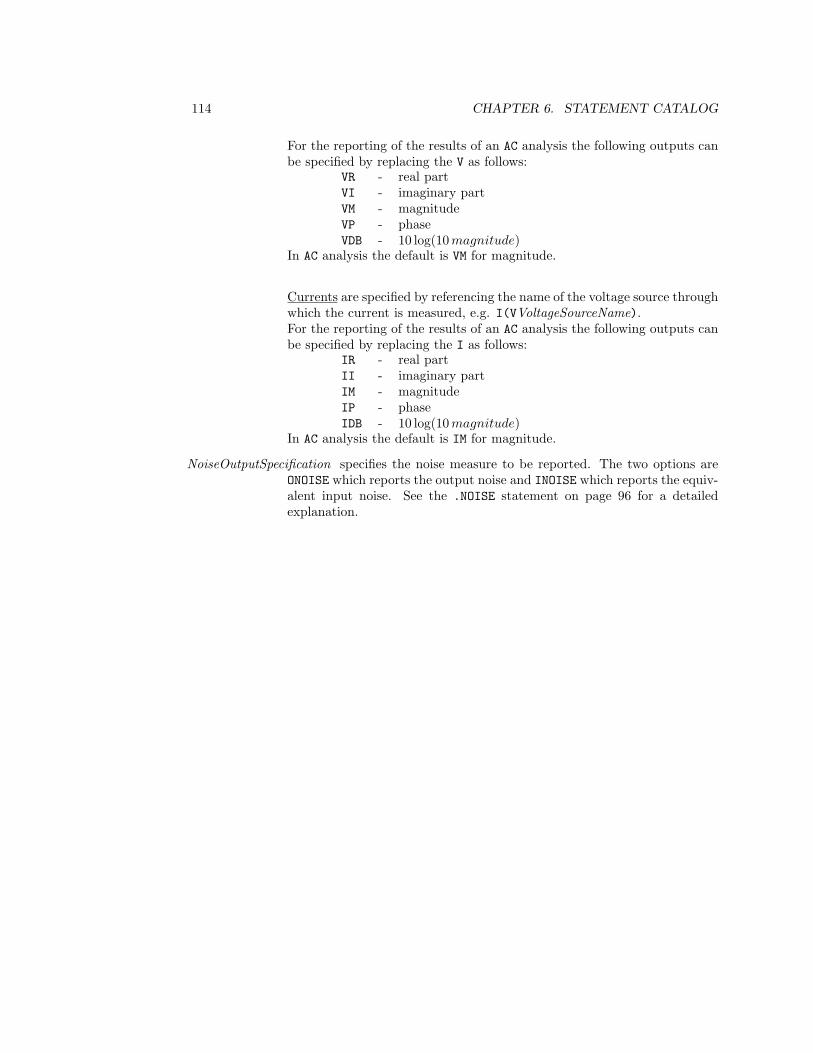
114 CHAPTER 6. STATEMENT CATALOG
For the reporting of the results of an AC analysis the following outputs canbe specified by replacing the V as follows:
VR - real partVI - imaginary partVM - magnitudeVP - phaseVDB - 10 log(10 magnitude)
In AC analysis the default is VM for magnitude.
Currents are specified by referencing the name of the voltage source throughwhich the current is measured, e.g. I(VVoltageSourceName).For the reporting of the results of an AC analysis the following outputs canbe specified by replacing the I as follows:
IR - real partII - imaginary partIM - magnitudeIP - phaseIDB - 10 log(10 magnitude)
In AC analysis the default is IM for magnitude.
NoiseOutputSpecification specifies the noise measure to be reported. The two options areONOISE which reports the output noise and INOISE which reports the equiv-alent input noise. See the .NOISE statement on page 96 for a detailedexplanation.

Print Specification 115
It must be one of the following:ONOISE - RMS output noise voltageDB(ONOISE) - output noise voltage in dB (= 20 log(ONOISE)INOISE - RMS equivalent input noise voltageDB(INOISE) - equivalent input noise voltage in dB (= 20 log(INOISE)GAIN - voltage gainDB(GAIN) - voltage gain in dB (= 20 log(GAIN)GT - transducer gainDB(GT) - transducer gain in dB (= 10 log(GT)NF - spot noise factorDB(NF) - spot noise figure (= 10 log(NF)SNR - output signal-to-noise ratioDB(SNR) - output signal-to-noise ratio in dB (= 20 log(SNR)TNOISE - output noise temperature.
SParameterOutputSpecification specifies the S-parameter output variables that are to beprinted. Each variable must have one of the following forms:
S(i,j) - Magnitude of Sij
SR(i,j) - Real part of Sij
SI(i,j) - Imaginary part of Sij
SP(i,j) - Phase of Sij in degreesSDB(i,j) - Magnitude of Sij in dB (= 20 log(S(i,j)))SG(i,j) - Group delay of Sij
The port numbers are i, j which are specified using the PNR keyword whenthe port element is specified.
DistortionOutputSpecification specifies the distortion component to be reported in a tabularformat of up to 8 columns plus an initial column with the sweep variable.The DistortionOutputSpecification is one of the following:
HD2 - the second harmonic distortionHD3 - the second harmonic distortionSIM2 - the sum frequency intermodulation componentDIM2 - the difference frequency intermodulation componentDIM3 - the third order intermodulation component
See the .DISTO statement on page 74 for a description of these distortioncomponents.
DistortionReportType specifies the format for reporting the distortion components. It mustbe one of the following:
R - real partI - imaginary partM - magnitudeP - phaseDB - 10 log(10 magnitude)
The default is M for magnitude.
Example

116 CHAPTER 6. STATEMENT CATALOG
.PRINT TRAN V(10) V(5,3) I(VIN)
.PRINT AC VM(10) VR(5,3) IP(VLOAD)
.PRINT DC V(10) V(5,3) I(VIN)
.PRINT NOISE ONOISE INOISE DB(ONOISE) DB(INOISE)
.PRINT NOISE GAIN DB(GT) DB(NF) SNR TNOISE
.PRINT AS SDB(1,1) SP(1,1) SDB(1,2) SP(1,2)
.PRINT DISTO HD2 HD3 SIM2(DB)
Note
1. There can be any number of .PRINT statements.
2. The number of significant digits of the results reported is NUMDGT which is set in a.OPTIONS statement (see page 103).
3. The current through any element can be found by inserting independent voltagesources in series with the elements. This is generally what is required in Spice2g6andSpice3. However PSpice supports direct specification of the voltage and currents ofmost elements. See the section on page 116.
Output Specification for PSpicePSpice supports a relatively large variety of output specifications compared to that avail-
able with Spice2g6 and Spice3. The output specifications described in the following canbe used .PRINT and .PLOT statements. The various forms of output specifications enablethe current and voltages of virtually all devices to be examined¿
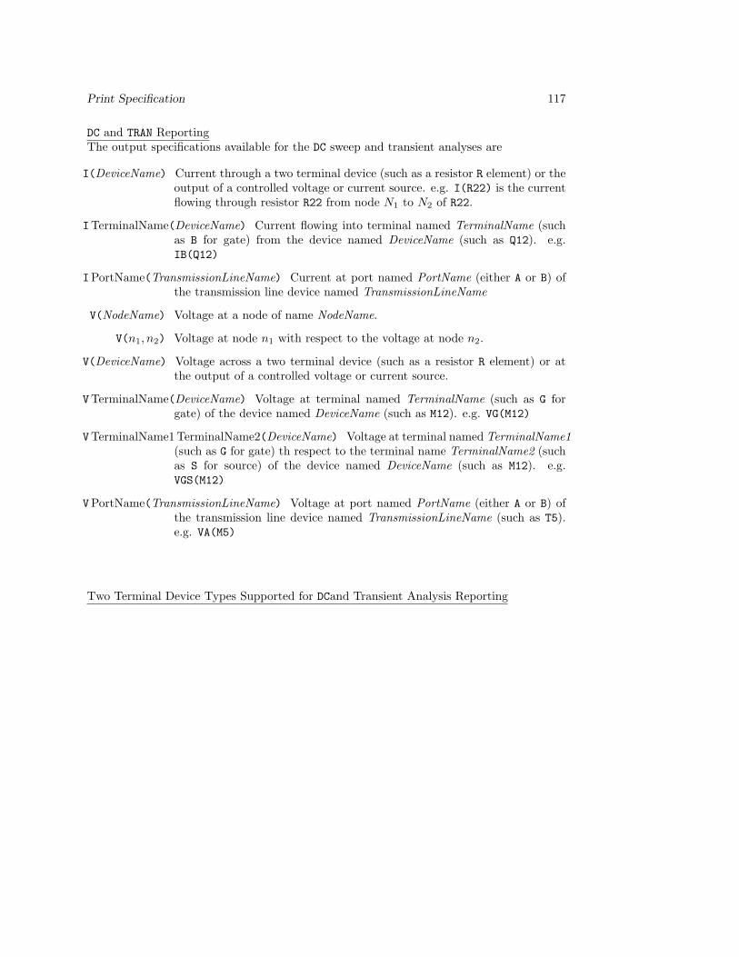
Print Specification 117
DC and TRAN ReportingThe output specifications available for the DC sweep and transient analyses are
I(DeviceName) Current through a two terminal device (such as a resistor R element) or theoutput of a controlled voltage or current source. e.g. I(R22) is the currentflowing through resistor R22 from node N1 to N2 of R22.
ITerminalName(DeviceName) Current flowing into terminal named TerminalName (suchas B for gate) from the device named DeviceName (such as Q12). e.g.IB(Q12)
IPortName(TransmissionLineName) Current at port named PortName (either A or B) ofthe transmission line device named TransmissionLineName
V(NodeName) Voltage at a node of name NodeName.
V(n1, n2) Voltage at node n1 with respect to the voltage at node n2.
V(DeviceName) Voltage across a two terminal device (such as a resistor R element) or atthe output of a controlled voltage or current source.
VTerminalName(DeviceName) Voltage at terminal named TerminalName (such as G forgate) of the device named DeviceName (such as M12). e.g. VG(M12)
VTerminalName1TerminalName2(DeviceName) Voltage at terminal named TerminalName1(such as G for gate) th respect to the terminal name TerminalName2 (suchas S for source) of the device named DeviceName (such as M12). e.g.VGS(M12)
VPortName(TransmissionLineName) Voltage at port named PortName (either A or B) ofthe transmission line device named TransmissionLineName (such as T5).e.g. VA(M5)
Two Terminal Device Types Supported for DCand Transient Analysis Reporting
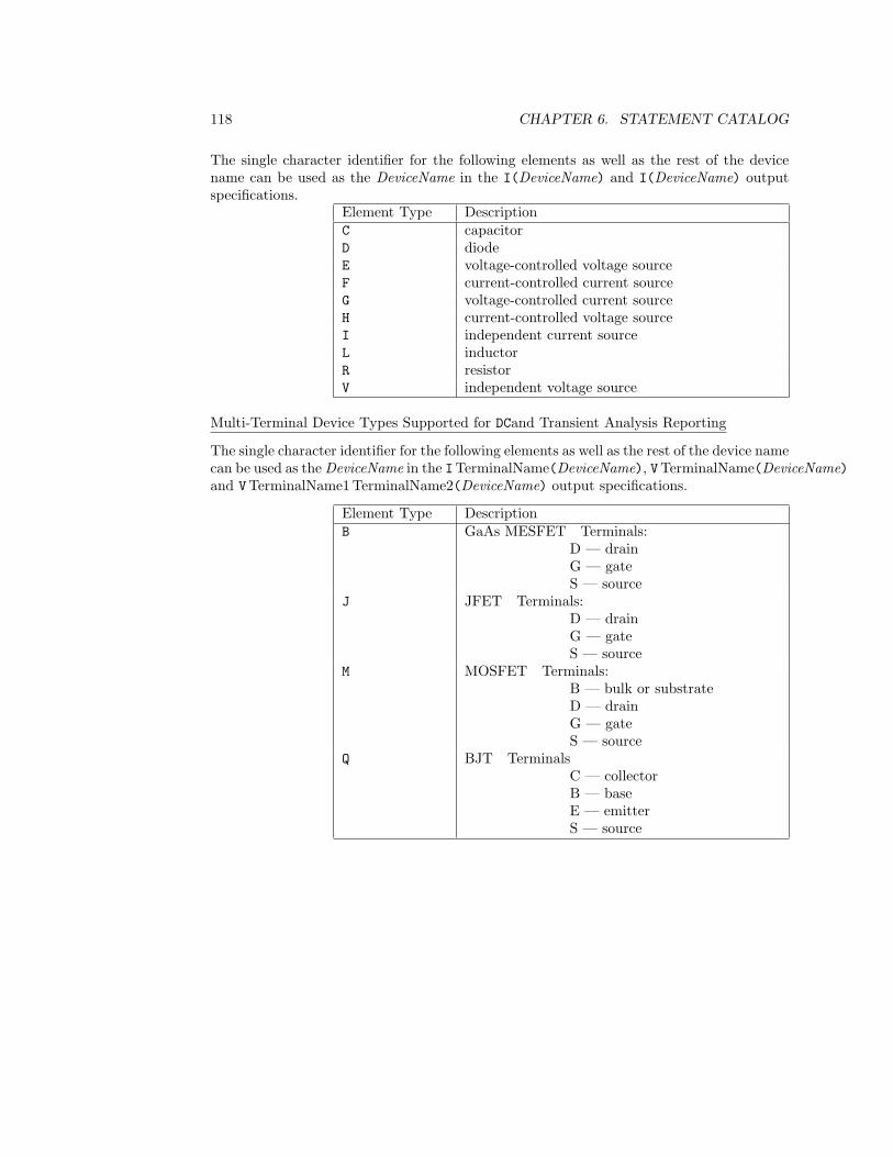
118 CHAPTER 6. STATEMENT CATALOG
The single character identifier for the following elements as well as the rest of the devicename can be used as the DeviceName in the I(DeviceName) and I(DeviceName) outputspecifications.
Element Type DescriptionC capacitorD diodeE voltage-controlled voltage sourceF current-controlled current sourceG voltage-controlled current sourceH current-controlled voltage sourceI independent current sourceL inductorR resistorV independent voltage source
Multi-Terminal Device Types Supported for DCand Transient Analysis Reporting
The single character identifier for the following elements as well as the rest of the device namecan be used as the DeviceName in the ITerminalName(DeviceName), VTerminalName(DeviceName)and VTerminalName1TerminalName2(DeviceName) output specifications.
Element Type DescriptionB GaAs MESFET Terminals:
D — drainG — gateS — source
J JFET Terminals:D — drainG — gateS — source
M MOSFET Terminals:B — bulk or substrateD — drainG — gateS — source
Q BJT TerminalsC — collectorB — baseE — emitterS — source

Print Specification 119
AC ReportingThe output specifications available for reporting the results of an AC frequency sweep anal-ysis includes all of the specification formats discussed above for DC and transient analysistogether with a number of possible suffixes:
DB - 10 log(10 magnitude)M - magnitudeP - phaseR - real partI - imaginary partG - group delay = ∂φ/∂f
where φ is the phase of the quantity being reported and fis the analysis frequency.
In AC analysis the default suffix is M for magnitude.
Two-Terminal Device Types Supported for AC Reporting
The single character identifier for the following elements as well as the rest of the devicename can be used as the DeviceName in the I(DeviceName) and I(DeviceName) outputspecifications.
Element Type DescriptionC capacitorD diodeI independent current sourceL inductorR resistorV independent voltage source
Multi-Terminal Device Types Supported for DCand Transient Analysis Reporting
The single character identifier for the following elements as well as the rest of the device namecan be used as the DeviceName in the ITerminalName(DeviceName), VTerminalName(DeviceName)and VTerminalName1TerminalName2(DeviceName) output specifications.
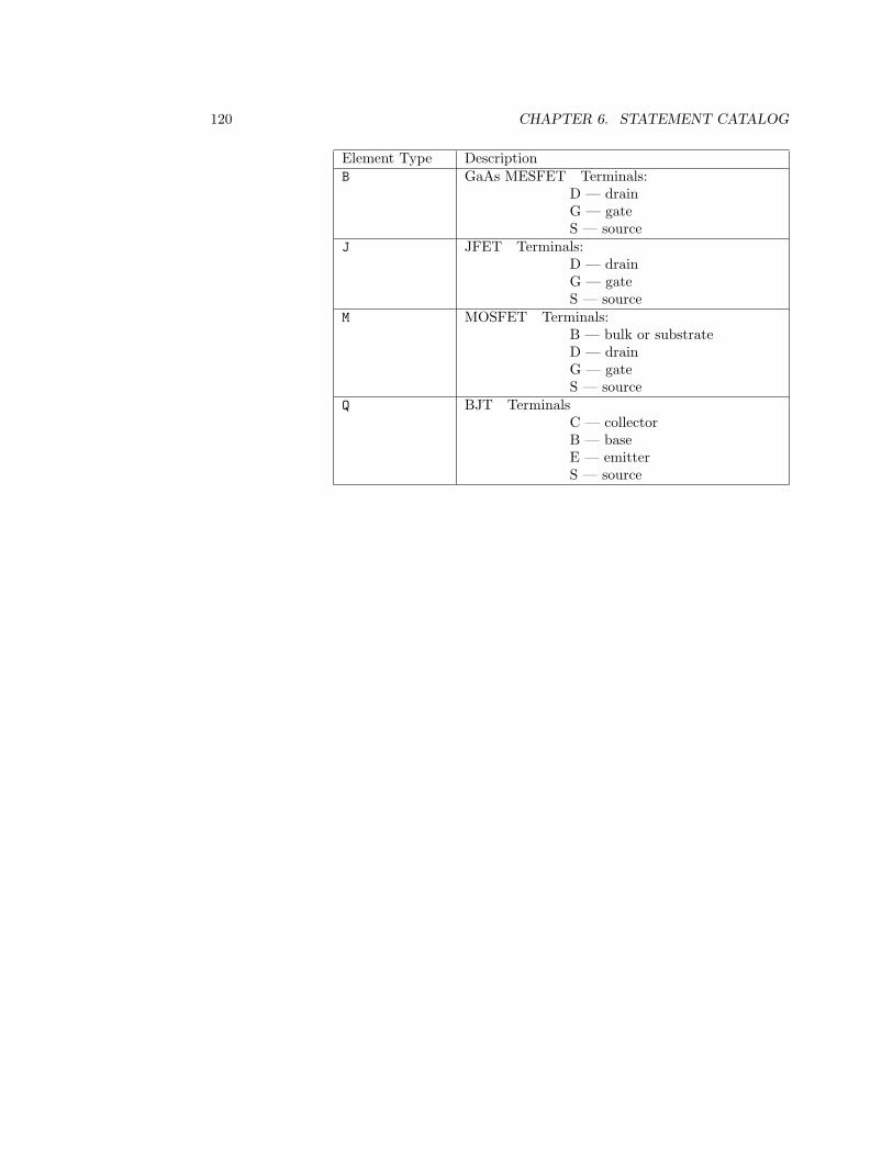
120 CHAPTER 6. STATEMENT CATALOG
Element Type DescriptionB GaAs MESFET Terminals:
D — drainG — gateS — source
J JFET Terminals:D — drainG — gateS — source
M MOSFET Terminals:B — bulk or substrateD — drainG — gateS — source
Q BJT TerminalsC — collectorB — baseE — emitterS — source

Data Output Specification:PSpice Only 121
Data Output Specification PSpice Only .PROBE
There is a big problem here — Probe is a trademark of Microsimcorporation
The .PROBE statement saves the node voltages and device currents in a file for subsequentprobing.PSpiceForm
.PROBE [/CSDF] [OutputSpecification . . . ]
/CSDF is a keyword resulting in the output probing file being written in ASCIIformat. By default the probing file is output in the more efficient binaryformat. However, only the ASCII formated is fully portable between com-puters and operating systems.
OutputSpecification specifies a node voltage or device current to be included in the probedata file. The output specifications supported are those supported forthe .PRINT and .PLOT statements. A comprehensive description of theOutputSpecification supported is given in the section on output specifi-cation on page 116.If an OutputSpecification is not given then all node voltages and devicecurrents are stored in the probing file.
Example
.PROBE V(10) V(5,3) I(VIN)
.PROBE VM(10) VR(5,3) IP(VLOAD)
.PROBE/CSDF V(10) IG(VIN)
.PROBE
The first example will output data from .DC, .AC and .TRAN analyses.
The second example will output data only from a .AC analysis.The third example will output the node voltage at node 10 for .DC, .AC and .TRAN analysesbut output the group delay of the current in the independent voltage source VIN only froman .AC analysis. As well the data will be output in ASCII format.The fourth example results in all node voltages and device currents being stored.
Note

122 CHAPTER 6. STATEMENT CATALOG
1. The probing data is stored in the file PROBE.DAT .
2. The results of DC, AC and transient analyses are saved. An OutputSpecification whichis unique to a particular type of analysis is ignored when the the results of analysesare being selected to storage. An example is VI(10) which selects the imaginary partof the voltage at node 10 and so only applies for storage of the results for an ACsmall-signal analysis.
3. The results stored in the probe file can subsequently be viewed using the Probeprogramdescribed in chapter ??.

Pole-Zero Analysis:Spice3Only 123
Pole-Zero Analysis Spice3Only .PZ
In pole zero analysis the poles and zeros of the small signal ACtransfer function of atwo-port is evaluated.
pfigpz.ps
Figure 6.1: Two port definition for pole-zero analysis.
Form
.PZ Node1 Node2 Node3 Node4 CUR POL
.PZ Node1 Node2 Node3 Node4 CUR ZER
.PZ Node1 Node2 Node3 Node4 CUR PZ
.PZ Node1 Node2 Node3 Node4 VOL POL
.PZ Node1 Node2 Node3 Node4 VOL ZER
.PZ Node1 Node2 Node3 Node4 VOL PZ
Node1 is the positive input node.
Node2 is the negative input node.
Node3 is the positive output node.
Node4 is the negative output node.
CUR is the keyword to evaluate the transfer function (output voltage)/(inputcurrent)
VOL is the keyword to evaluate the transfer function (output voltage)/(inputvoltage)
POL is the keyword to evaluate the poles of the transfer function only.
ZERO is the keyword to evaluate the zeroes of the transfer function only.
PZ is the keyword to evaluate the poles and zeroes of the transfer function.
Example
.PZ 1 0 3 0 CUR POL
.PZ 2 3 5 0 VOL ZER
.PZ 4 1 4 1 CUR PZ
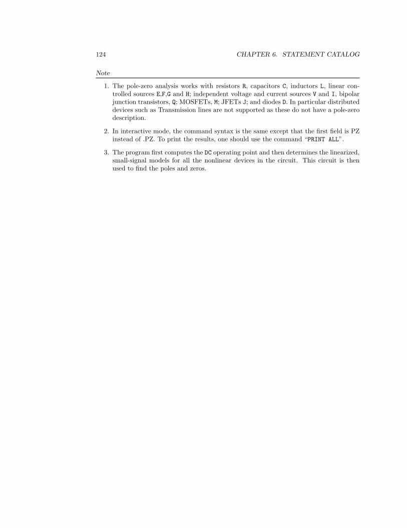
124 CHAPTER 6. STATEMENT CATALOG
Note
1. The pole-zero analysis works with resistors R, capacitors C, inductors L, linear con-trolled sources E,F,G and H; independent voltage and current sources V and I, bipolarjunction transistors, Q; MOSFETs, M; JFETs J; and diodes D. In particular distributeddevices such as Transmission lines are not supported as these do not have a pole-zerodescription.
2. In interactive mode, the command syntax is the same except that the first field is PZinstead of .PZ. To print the results, one should use the command “PRINT ALL”.
3. The program first computes the DC operating point and then determines the linearized,small-signal models for all the nonlinear devices in the circuit. This circuit is thenused to find the poles and zeros.

Save Bias Conditions:PSpice92 Only 125
Save Bias Conditions PSpice92 Only .SAVEBIAS
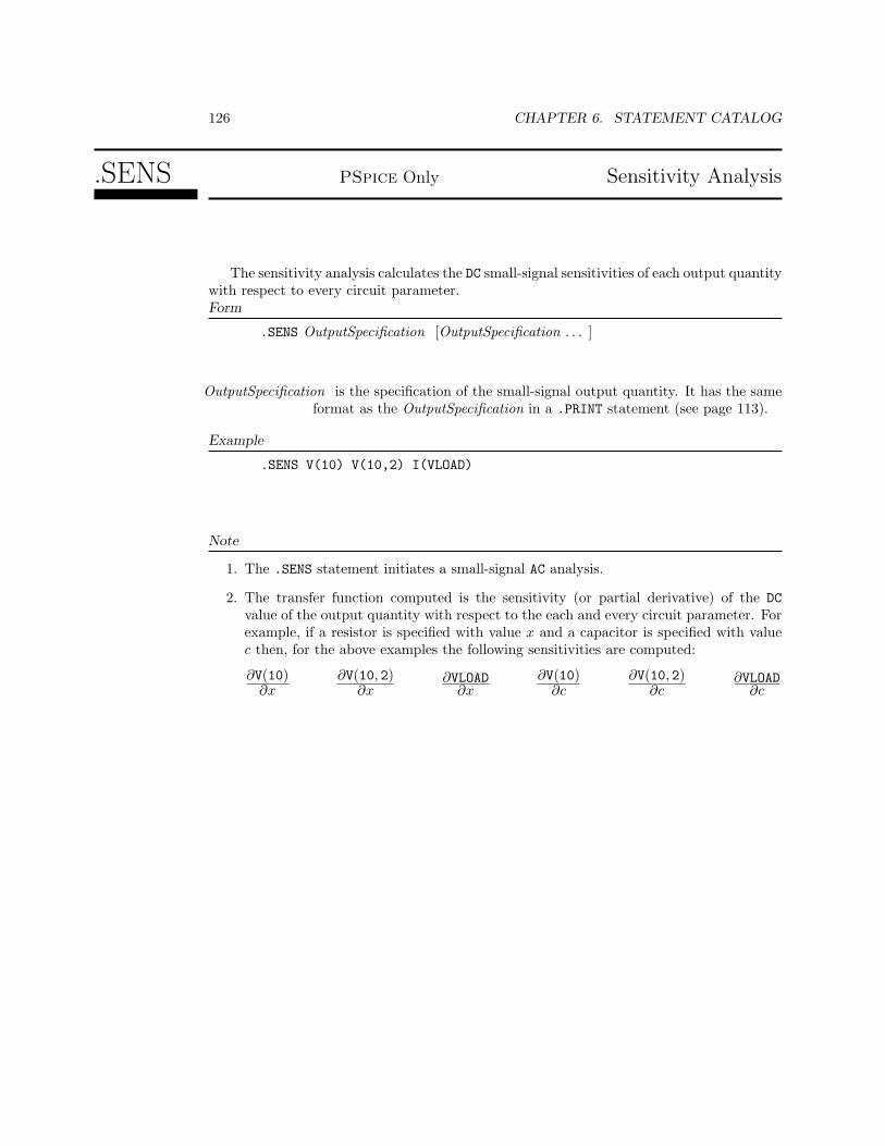
126 CHAPTER 6. STATEMENT CATALOG
.SENS PSpice Only Sensitivity Analysis
The sensitivity analysis calculates the DC small-signal sensitivities of each output quantitywith respect to every circuit parameter.Form
.SENS OutputSpecification [OutputSpecification . . . ]
OutputSpecification is the specification of the small-signal output quantity. It has the sameformat as the OutputSpecification in a .PRINT statement (see page 113).
Example
.SENS V(10) V(10,2) I(VLOAD)
Note
1. The .SENS statement initiates a small-signal AC analysis.
2. The transfer function computed is the sensitivity (or partial derivative) of the DCvalue of the output quantity with respect to the each and every circuit parameter. Forexample, if a resistor is specified with value x and a capacitor is specified with valuec then, for the above examples the following sensitivities are computed:
∂V(10)∂x
∂V(10, 2)∂x
∂VLOAD∂x
∂V(10)∂c
∂V(10, 2)∂c
∂VLOAD∂c

Parameteric Analysis:PSpice92 Only 127
Parameteric Analysis PSpice92 Only .STEP
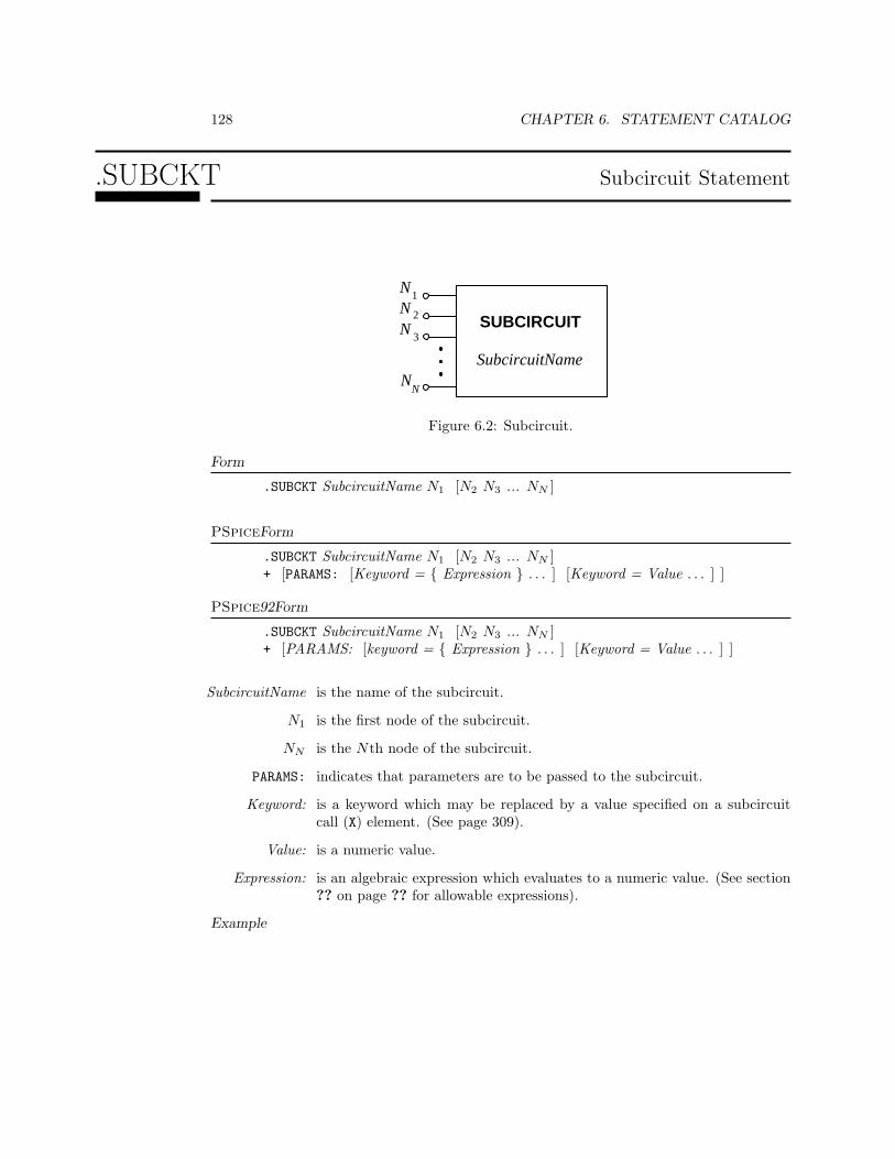
128 CHAPTER 6. STATEMENT CATALOG
.SUBCKT Subcircuit Statement
1
2
3SUBCIRCUIT
SubcircuitName
NN
NNN
Figure 6.2: Subcircuit.
Form
.SUBCKT SubcircuitName N1 [N2 N3 ... NN ]
PSpiceForm
.SUBCKT SubcircuitName N1 [N2 N3 ... NN ]+ [PARAMS: [Keyword = Expression . . . ] [Keyword = Value . . . ] ]
PSpice92Form
.SUBCKT SubcircuitName N1 [N2 N3 ... NN ]+ [PARAMS: [keyword = Expression . . . ] [Keyword = Value . . . ] ]
SubcircuitName is the name of the subcircuit.
N1 is the first node of the subcircuit.
NN is the Nth node of the subcircuit.
PARAMS: indicates that parameters are to be passed to the subcircuit.
Keyword: is a keyword which may be replaced by a value specified on a subcircuitcall (X) element. (See page 309).
Value: is a numeric value.
Expression: is an algebraic expression which evaluates to a numeric value. (See section?? on page ?? for allowable expressions).
Example

Subcircuit Statement 129
.SUBCKT MULTI 2 4 17 3 1

130 CHAPTER 6. STATEMENT CATALOG
.SUBCKT
Note
1. The global ground node, node 0 (or in PSpice node GND) must not be one of thesubcircuit nodes.
2. Subcircuits are incorporated by using the “X” element. The number of nodes of the“X” element must correspond to the number of nodes in the definition of the subcircuit(i.e. is in the .SUBCKT statement). See page 309 for a description of the X element.
3. The last line in a subcircuit definition is the .ENDS line (see page 80).
4. The only restriction on the statements within a subcircuit is that control lines such as.AC, .DC or .OPTIONS are not allowed. However, element lines, model statements andother subcircuit definitions and subcircuit calls are allowed.
5. Device models or subcircuit definitions included as part of a subcircuit definitionare local only. Subcircuits and models that are to be “known” by all elements andsubcircuits must be defined at the top level of the circuit hierarchy.
6. The nodes of elements in the subcircuit definition are local except for those that alsoappear on the .SUBCKT statement and for the ground (0) node. The local nodes aregiven the unique name
SubcircuitName1:[SubcircuitName2: . . . ]LocalNodeName .and local devices are given the unique name
DeviceType:SubcircuitName1:[SubcircuitName2 . . . ]DeviceName .

Temperature Specification 131
Temperature Specification .TEMP
The .TEMP statement specifies the temperatures at which the circuit is to be simulated.Form
.TEMP T1 [T2 . . . TN ]
T1 is the first temperature at which the circuit is to be simulated.
TN is the Nth temperature at which the circuit is to be simulated.
Note
1. The circuit is first simulated at temperature T1 and then resimulated at temperatureT2 and so on.
2. If the .TEMP statement is missing then T1 is assumed to be TNOM specified in a.OPTIONS statement.
3. Model parameters are specified at TNOM and prior to the simulation at a new temper-ature temperature dependent device parameters are reevaluated.

132 CHAPTER 6. STATEMENT CATALOG
.TEXT PSpice92 Only Text Parameter Definition
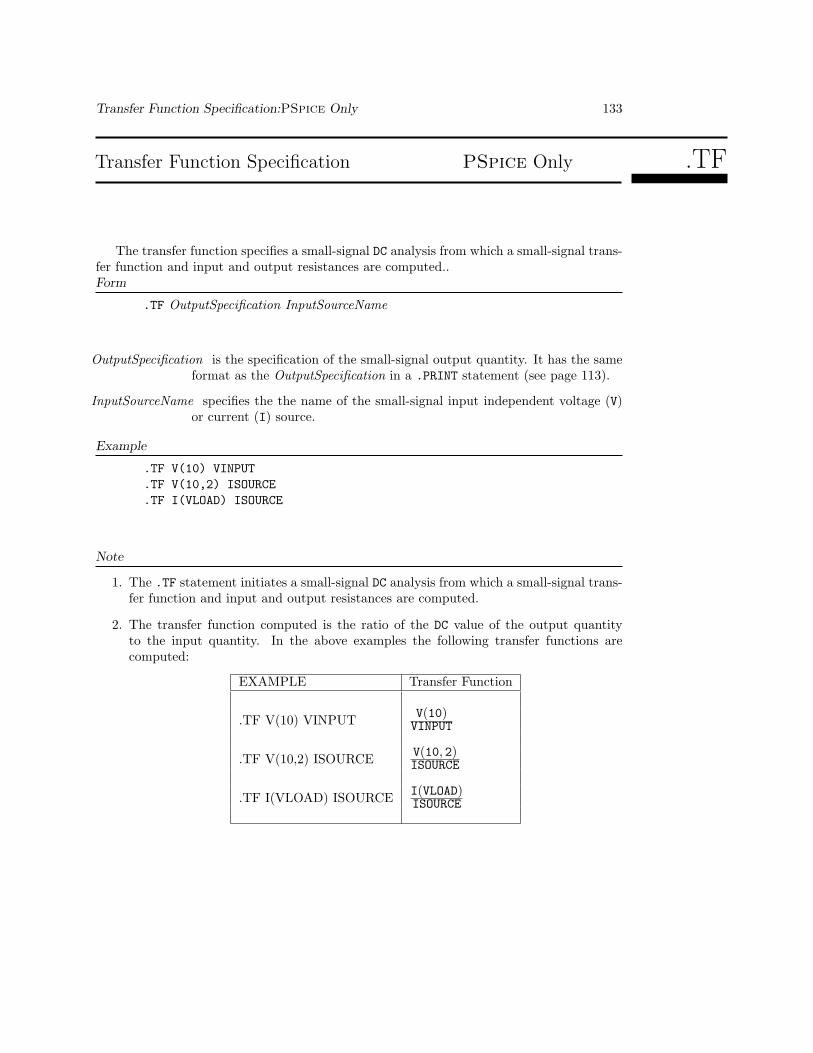
Transfer Function Specification:PSpice Only 133
Transfer Function Specification PSpice Only .TF
The transfer function specifies a small-signal DC analysis from which a small-signal trans-fer function and input and output resistances are computed..Form
.TF OutputSpecification InputSourceName
OutputSpecification is the specification of the small-signal output quantity. It has the sameformat as the OutputSpecification in a .PRINT statement (see page 113).
InputSourceName specifies the the name of the small-signal input independent voltage (V)or current (I) source.
Example
.TF V(10) VINPUT
.TF V(10,2) ISOURCE
.TF I(VLOAD) ISOURCE
Note
1. The .TF statement initiates a small-signal DC analysis from which a small-signal trans-fer function and input and output resistances are computed.
2. The transfer function computed is the ratio of the DC value of the output quantityto the input quantity. In the above examples the following transfer functions arecomputed:
EXAMPLE Transfer Function
.TF V(10) VINPUT V(10)VINPUT
.TF V(10,2) ISOURCE V(10, 2)ISOURCE
.TF I(VLOAD) ISOURCE I(VLOAD)ISOURCE

134 CHAPTER 6. STATEMENT CATALOG
TITLE Title Line
The TITLE line must be the first line of the input file. The string on this line includedas the banner in the output log file appearing at the top of each page.
Transient Analysis 135
Transient Analysis .TRAN
In transient analysis the current and voltages in a circuit are computed as a function oftime.
General form:Form
.TRAN TSTEP TSTOP [TSTART [TMAX] ] [UIC]
TSTEP is the time increment for reporting transient simulation results.(Units: s)
TSTOP is the final analysis time.(Units: s)
TSTART is the start time for reporting the transient results. Transient analysisalways begins at time 0. Before the time TSTART no results are recorded.(Units: s; Optional; Default: 0)
TMAX is the maximum step size used in incrementing the time during transientanalysis.(Units: s; Optional; Default: the smaller of TSTEP and (TSTOP-TSTART)/50)
UIC is the optional keyword to use initial conditions specified on the elementline, by a .IC statement or a .NODESET statement. Normally the operatingpoint is determined (using a DC analysis) before a transient analysis isinitiated. If the UIC keyword is present the initial DC analysis is omittedand instead the initial conditions specified by the IC parameter supportedby certain elements, by the .IC statement, or by the .NODESET statementare used. In addition PSpice supports using an operating point solutionthat was previously saved using the .SAVEBIAS statement.
Example
.TRAN 1NS 100NS
.TRAN 1NS 1000NS 500NS
.TRAN 10NS 1US UIC
Note
136 CHAPTER 6. STATEMENT CATALOG
1. If the UIC keyword is not present a DC analysis is automatically performed prior toa transient (.TRAN) analysis to find the operating point of the circuit. All sourceswhich are not time dependent (for example, power supplies) are set to their DC value.The transient time interval is specified on a .TRAN control line. The operating pointsolution is used as the initial conditions for a transient analysis. Individual operatingpoint solutions are overridden by initial transient conditions specified on the .TRANstatement or by the initial conditions specified for specific elements by the IC keyword.
2. Normally the operating point is determined (using a DC analysis) before a transientanalysis is initiated. If the UIC keyword is present the initial DC analysis is omittedand instead the initial conditions specified by the IC parameter supported by certainelements, by the .IC statement (see 83), or by the .NODESET statement (see 95) areused. In addition PSpice supports using an operating point solution that waspreviously saved using the .SAVEBIAS statement described on page 125.
3. If the UIC keyword is present the initial conditions specified in the .IC statement(described on page 83) are used to establish the initial conditions. Initial conditionsspecified for individual elements using the IC parameter on the element line will alwayshave precedence over those specified in a .IC statement.No DC analysis is performed prior to a transient analysis. Thus it is important toestablish the initial conditions at all nodes using the .IC statement or using the ICelement parameter.

Watch Analysis Statement:PSpice92 Only 137
Watch Analysis Statement PSpice92 Only .WATCH

138 CHAPTER 6. STATEMENT CATALOG
.WCASE PSpice92 Only Sensitivity and Worst Case Analysis
The sensitivity and worst case analysis is a statistical analysis of a circuit causing thecircuit to analyzed many times with a random change of model parameters (parameters ina .MODEL statement).Form
.WCASE NumberOfRuns AnalysisType OutputSpecification OutputFunction [LIST]+ [OUTPUT(OutputSampleType )] [RANGE(LowValue, HighValue)]
Sensitivity and Worst Case Analysis:PSpice92 Only 139
NumberOfRuns is the total number of runs to do. This number includes the initial nominalrun.
AnalysisType is the type of analysis to be performed in Monte Carlo runs after the initialnominal run. All analyses specified in the NETLIST are performed in thenominal run. The AnalysisType must be one of the following:
to be filled in
DC is a keyword indicating that the DC analysis as specified by the .DC state-ment is repeated. The sweep variable used in analyzing the output Out-putSpecification is the value of the independent voltage or current sourcespecified in the .DC statement which is discussed on page 70.
AC is a keyword indicating that the AC small-signal analysis as specified by the.AC statement is repeated. The sweep variable used in analyzing the outputOutputSpecification is frequency.
TRAN is a keyword indicating that the transient analysis as specified by the .TRANstatement is repeated. The sweep variable used in analyzing the outputOutputSpecification is time.
OutputSpecification specifies the quantity to be reported as the result of the Monte CarloAnalysis. It has the same format as the OutputSpecification in a .PRINTstatement (see page 113). The result is the value of the OutputSpecificationwith respect to a sweep for DC and AC analysis, and as a waveform for TRANanalysis.
OutputFunction indicates the function to be performed on the output indicated by Out-putSpecification to reduce the sweep or waveform at each run to a singlenumeric value. The OutputFunction must be one of the following key-words:
YMAX which produces the greatest deviation of the sweep or wave-form from the nominal run.
MAX which results in the maximum value in each sweep or wave-form.
MIN which results in the minimum value in each sweep or wave-form.
RISE EDGE(Value) which reports as the result the first run when the wave-form crosses above the threshold Value. The algorithmused requires that one point in the waveform be belowValue and the succeeding point be above Value.
FALL EDGE(Value) which reports as the result the first run when the wave-form crosses below the threshold Value. The algorithmused requires that one point in the waveform be aboveValue and the succeeding point be below Value.
RANGE is an optional range indicating the range of the sweep variable over whichOutputFunction is to be performed. If this keyword is missing output isproduced the range is not restricted. The range of the sweep variable to beconsidered is from LowValue to HighValue inclusive.
LowValue is the low end of the sweep variable to be considered in evaluating Output-Function.
HighValue is the low end of the sweep variable to be considered in evaluating Output-Function.
LIST is an optional keyword that results in the model parameter values that arestatistically varied being printed out prior to each run. If it is omitted thenthe the statistically generated model parameter values are not producedprior to each run.
OUTPUT is an optional keyword indicating the type of output to be produced by runsafter the initial nominal run. The output produced for each run sampled isdetermined by the .PLOT, .PRINT and .PROBE statements in the NETLIST.If this keyword is missing output is produced only for the nominal run.
SEED is the keyword for the seed of the random number generator used in MonteCarlo Analysis
SeedValue is the value of the seed used in the random number generator used toselect sample runs at random. (Optional; Default: 17,533; 1 ≤ SeedValue≤32, 767)
Note

140 CHAPTER 6. STATEMENT CATALOG
1. If the AnalysisType is DC only one independent voltage or current source can be spec-ified in the .DC statement (discussed on page 70).
2. The random number generator is the subtractive method generator described by Knuth[28, p. 171].
3. The initial run uses the nominal parameter values given in the NETLIST. Subsequentruns statistically vary model parameters indicated as having either lot LOT or deviceDEV tolerances. These tolerances are specified in a .MODEL statement (see page 90).

Width Specification 141
Width Specification .WIDTH
Form
.WIDTH OUT=ColumnWidth
OUT is the keyword for column width of the output file.
ColumnWidth is the column width of the output file. It must be either 80 or 132. If thereis no .WIDTH statement the ColumnWidth defaults to 80.
Example
.WIDTH OUT=80
.WIDTH OUT=132

142 CHAPTER 6. STATEMENT CATALOG
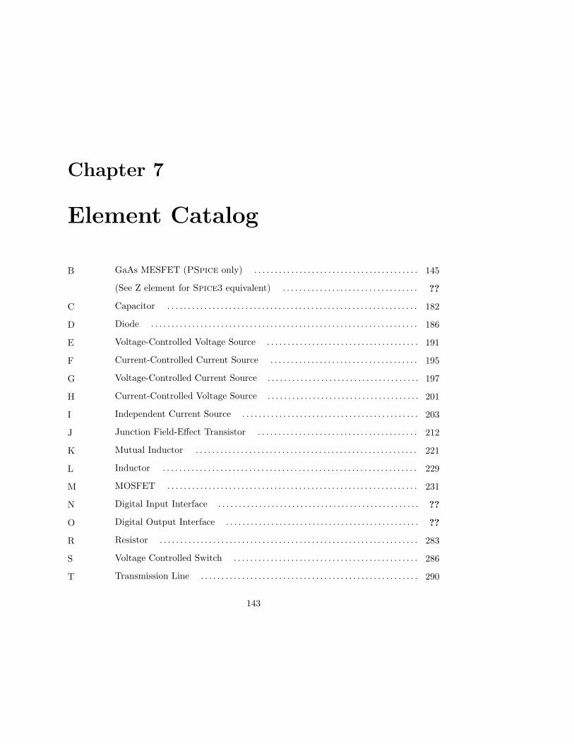
Chapter 7
Element Catalog
B GaAs MESFET (PSpice only) . . . . . . . . . . . . . . . . . . . . . . . . . . . . . . . . . . . . . . . . 145
(See Z element for Spice3 equivalent) . . . . . . . . . . . . . . . . . . . . . . . . . . . . . . . . . ??
C Capacitor . . . . . . . . . . . . . . . . . . . . . . . . . . . . . . . . . . . . . . . . . . . . . . . . . . . . . . . . . . . . . 182
D Diode . . . . . . . . . . . . . . . . . . . . . . . . . . . . . . . . . . . . . . . . . . . . . . . . . . . . . . . . . . . . . . . . . 186
E Voltage-Controlled Voltage Source . . . . . . . . . . . . . . . . . . . . . . . . . . . . . . . . . . . . . 191
F Current-Controlled Current Source . . . . . . . . . . . . . . . . . . . . . . . . . . . . . . . . . . . . 195
G Voltage-Controlled Current Source . . . . . . . . . . . . . . . . . . . . . . . . . . . . . . . . . . . . . 197
H Current-Controlled Voltage Source . . . . . . . . . . . . . . . . . . . . . . . . . . . . . . . . . . . . . 201
I Independent Current Source . . . . . . . . . . . . . . . . . . . . . . . . . . . . . . . . . . . . . . . . . . . 203
J Junction Field-Effect Transistor . . . . . . . . . . . . . . . . . . . . . . . . . . . . . . . . . . . . . . . 212
K Mutual Inductor . . . . . . . . . . . . . . . . . . . . . . . . . . . . . . . . . . . . . . . . . . . . . . . . . . . . . . 221
L Inductor . . . . . . . . . . . . . . . . . . . . . . . . . . . . . . . . . . . . . . . . . . . . . . . . . . . . . . . . . . . . . . 229
M MOSFET . . . . . . . . . . . . . . . . . . . . . . . . . . . . . . . . . . . . . . . . . . . . . . . . . . . . . . . . . . . . . 231
N Digital Input Interface . . . . . . . . . . . . . . . . . . . . . . . . . . . . . . . . . . . . . . . . . . . . . . . . . ??
O Digital Output Interface . . . . . . . . . . . . . . . . . . . . . . . . . . . . . . . . . . . . . . . . . . . . . . . ??
R Resistor . . . . . . . . . . . . . . . . . . . . . . . . . . . . . . . . . . . . . . . . . . . . . . . . . . . . . . . . . . . . . . . 283
S Voltage Controlled Switch . . . . . . . . . . . . . . . . . . . . . . . . . . . . . . . . . . . . . . . . . . . . . 286
T Transmission Line . . . . . . . . . . . . . . . . . . . . . . . . . . . . . . . . . . . . . . . . . . . . . . . . . . . . . 290
143

144 CHAPTER 7. ELEMENT CATALOG
U Digital Device . . . . . . . . . . . . . . . . . . . . . . . . . . . . . . . . . . . . . . . . . . . . . . . . . . . . . . . . . 294
U Lossy RC Transmission Line . . . . . . . . . . . . . . . . . . . . . . . . . . . . . . . . . . . . . . . . . . . ??
V Independent Voltage Source . . . . . . . . . . . . . . . . . . . . . . . . . . . . . . . . . . . . . . . . . . . 297
W Current Controlled Switch . . . . . . . . . . . . . . . . . . . . . . . . . . . . . . . . . . . . . . . . . . . . . 306
X Subcircuit Call . . . . . . . . . . . . . . . . . . . . . . . . . . . . . . . . . . . . . . . . . . . . . . . . . . . . . . . . 309
Z MESFET . . . . . . . . . . . . . . . . . . . . . . . . . . . . . . . . . . . . . . . . . . . . . . . . . . . . . . . . . . . . . ??
(See B element for PSpice equivalent) . . . . . . . . . . . . . . . . . . . . . . . . . . . . . . . . . . . . . . . . . . . . 145
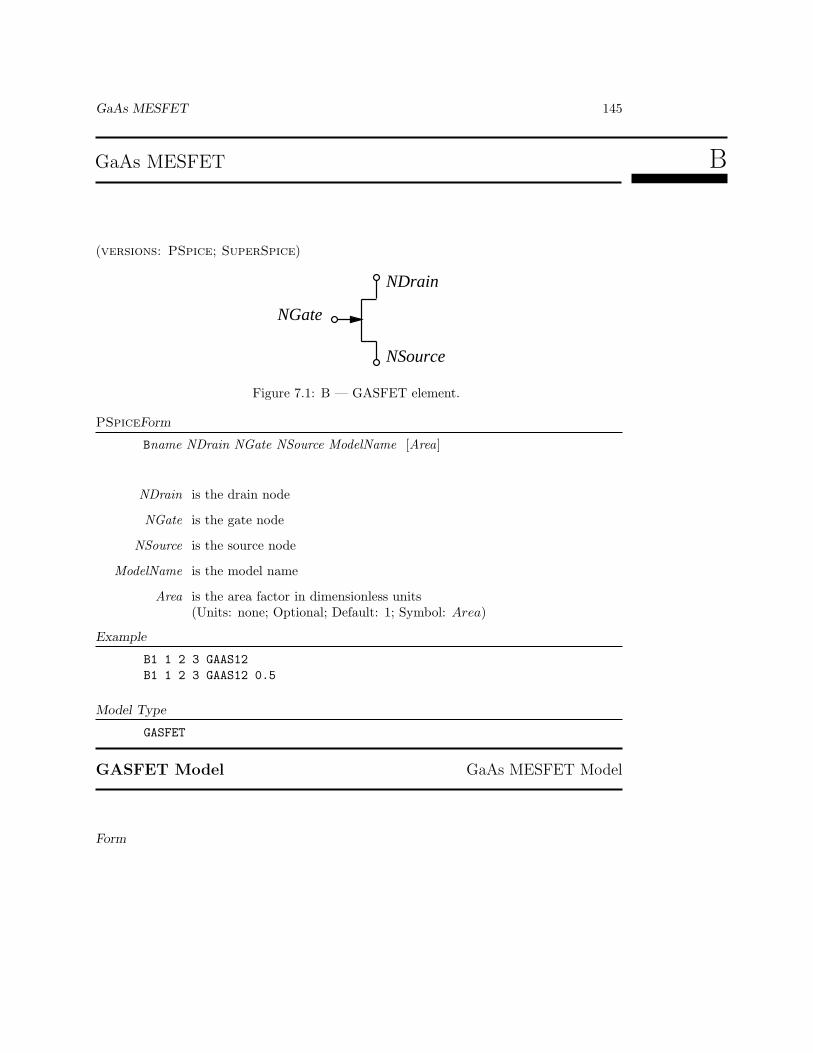
GaAs MESFET 145
GaAs MESFET B
(versions: PSpice; SuperSpice)
NGate
NDrain
NSource
Figure 7.1: B — GASFET element.
PSpiceForm
Bname NDrain NGate NSource ModelName [Area]
NDrain is the drain node
NGate is the gate node
NSource is the source node
ModelName is the model name
Area is the area factor in dimensionless units(Units: none; Optional; Default: 1; Symbol: Area)
Example
B1 1 2 3 GAAS12B1 1 2 3 GAAS12 0.5
Model Type
GASFET
GASFET Model GaAs MESFET Model
Form
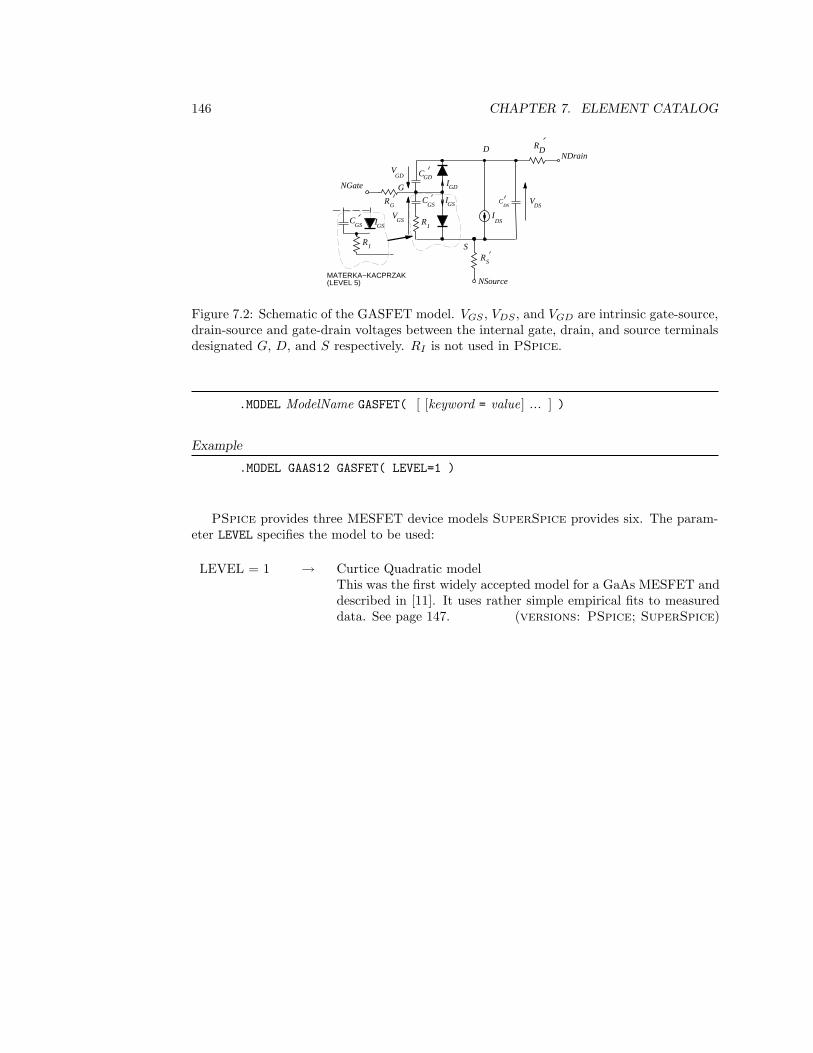
146 CHAPTER 7. ELEMENT CATALOG
NGate G
S
NSource
NDrainD
RG
IDS
VGS
CGS
RI
IGD
IGS
RS
RD
CGDV
GD
CDS
CGS
RI
IGS
MATERKA−KACPRZAK(LEVEL 5)
VDS
Figure 7.2: Schematic of the GASFET model. VGS , VDS , and VGD are intrinsic gate-source,drain-source and gate-drain voltages between the internal gate, drain, and source terminalsdesignated G, D, and S respectively. RI is not used in PSpice.
.MODEL ModelName GASFET( [ [keyword = value] ... ] )
Example
.MODEL GAAS12 GASFET( LEVEL=1 )
PSpice provides three MESFET device models SuperSpice provides six. The param-eter LEVEL specifies the model to be used:
LEVEL = 1 → Curtice Quadratic modelThis was the first widely accepted model for a GaAs MESFET anddescribed in [11]. It uses rather simple empirical fits to measureddata. See page 147. (versions: PSpice; SuperSpice)
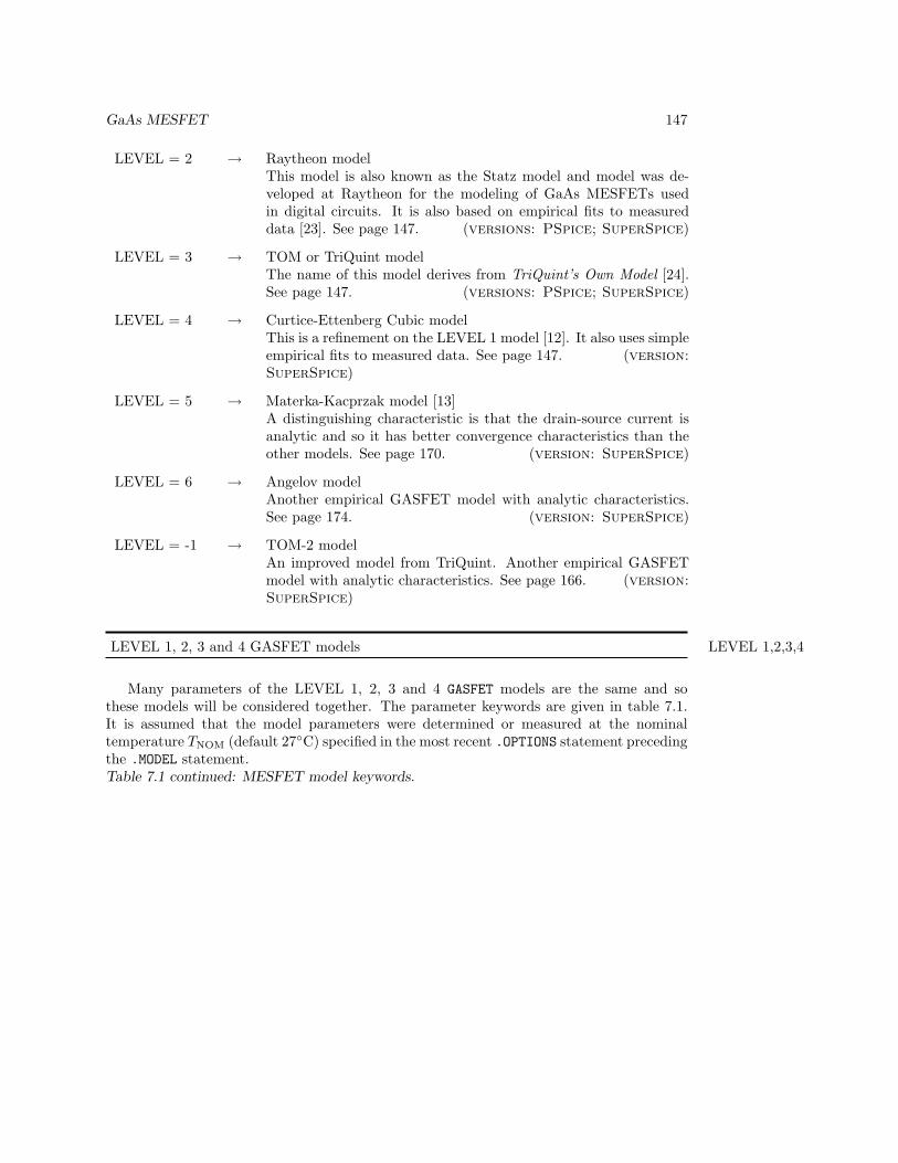
GaAs MESFET 147
LEVEL = 2 → Raytheon modelThis model is also known as the Statz model and model was de-veloped at Raytheon for the modeling of GaAs MESFETs usedin digital circuits. It is also based on empirical fits to measureddata [23]. See page 147. (versions: PSpice; SuperSpice)
LEVEL = 3 → TOM or TriQuint modelThe name of this model derives from TriQuint’s Own Model [24].See page 147. (versions: PSpice; SuperSpice)
LEVEL = 4 → Curtice-Ettenberg Cubic modelThis is a refinement on the LEVEL 1 model [12]. It also uses simpleempirical fits to measured data. See page 147. (version:SuperSpice)
LEVEL = 5 → Materka-Kacprzak model [13]A distinguishing characteristic is that the drain-source current isanalytic and so it has better convergence characteristics than theother models. See page 170. (version: SuperSpice)
LEVEL = 6 → Angelov modelAnother empirical GASFET model with analytic characteristics.See page 174. (version: SuperSpice)
LEVEL = -1 → TOM-2 modelAn improved model from TriQuint. Another empirical GASFETmodel with analytic characteristics. See page 166. (version:SuperSpice)
LEVEL 1, 2, 3 and 4 GASFET models LEVEL 1,2,3,4
Many parameters of the LEVEL 1, 2, 3 and 4 GASFET models are the same and sothese models will be considered together. The parameter keywords are given in table 7.1.It is assumed that the model parameters were determined or measured at the nominaltemperature TNOM (default 27C) specified in the most recent .OPTIONS statement precedingthe .MODEL statement.Table 7.1 continued: MESFET model keywords.
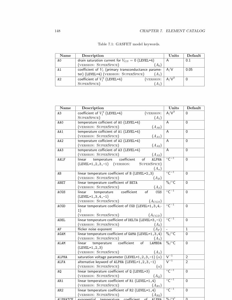
148 CHAPTER 7. ELEMENT CATALOG
Table 7.1: GASFET model keywords.
Name Description Units DefaultA0 drain saturation current for VGS = 0 (LEVEL=4)
(version: SuperSpice) (A0)A 0.1
A1 coefficient of V1 (primary transconductance parame-ter) (LEVEL=4) (version: SuperSpice) (A1)
A/V 0.05
A2 coefficient of V 21 (LEVEL=4) (version:
SuperSpice) (A1)A/V2 0
Name Description Units DefaultA3 coefficient of V 3
1 (LEVEL=4) (version:SuperSpice) (A1)
A/V3 0
AA0 temperature cofficient of A0 (LEVEL=4)(version: SuperSpice) (AA0)
A 0
AA1 temperature cofficient of A1 (LEVEL=4)(version: SuperSpice) (AA1)
A 0
AA2 temperature cofficient of A2 (LEVEL=4)(version: SuperSpice) (AA2)
A 0
AA3 temperature cofficient of A3 (LEVEL=4)(version: SuperSpice) (AA3)
A 0
AALF linear temperature coefficient of ALPHA(LEVEL=1,2,3,-1) (version: SuperSpice)
(Aα)
C−1 0
AB linear temperature coefficient of B (LEVEL=2,3)(version: SuperSpice) (AB)
C−1 0
ABET linear temperature coefficient of BETA(version: SuperSpice) (Aβ)
%/C 0
ACGS linear temperature coefficient of CGS(LEVEL=1,3,4,-1)(version: SuperSpice) (ACGS)
C−1 0
ACGD linear temperature coefficient of CGD (LEVEL=1,3,4,-1)(version: SuperSpice) (ACGD)
C−1 0
ADEL linear temperature coefficient of DELTA (LEVEL=3,-1)(version: SuperSpice) (Aδ)
C−1 0
AF flicker noise exponent (AF ) - 1AGAM linear temperature coefficient of GAMA (LEVEL=1,3,4)
(version: SuperSpice) (Aλ)%/C 0
ALAM linear temperature coefficient of LAMBDA(LEVEL=1,2,3)(version: SuperSpice) (Aλ)
%/C 0
ALPHA saturation voltage parameter (LEVEL=1,2,3,-1) (α) V−1 2
ALFA alternative keyword of ALPHA (LEVEL=1,2,3,-1)(version: SuperSpice) (α)
V−1 2
AQ linear temperature coefficient of Q (LEVEL=3)(version: SuperSpice) (AQ)
C−1 0
AR1 linear temperature coefficient of R1 (LEVEL=1,4)(version: SuperSpice) (AR1)
C−1 0
AR2 linear temperature coefficient of R2 (LEVEL=1,4)(version: SuperSpice) (AR2)
C−1 0
ALPHATCE exponential temperature coefficient of ALPHA(LEVEL=-1)(version: SuperSpice) (TC,α)
%/C 0
Table 7.1 continued: MESFET model keywords.
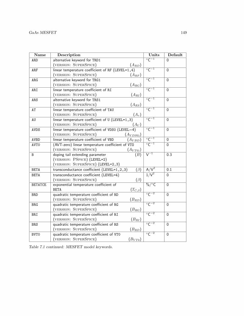
GaAs MESFET 149
Name Description Units DefaultARD alternative keyword for TRD1
(version: SuperSpice) (ARD)
C−1 0
ARF linear temperature coefficient of RF (LEVEL=1,4)(version: SuperSpice) (ARF )
C−1 0
ARG alternative keyword for TRG1(version: SuperSpice) (ARG)
C−1 0
ARI linear temperature coefficient of RI(version: SuperSpice) (ARI)
C−1 0
ARS alternative keyword for TRS1(version: SuperSpice) (ARS)
C−1 0
AT linear temperature coefficient of TAU(version: SuperSpice) (Aτ )
C−1 0
AU linear temperature coefficient of U (LEVEL=1,3)(version: SuperSpice) (AU )
C−1 0
AVDS linear temperature coefficient of VDS0 (LEVEL=4)(version: SuperSpice) (AV DS0))
C−1 0
AVBD linear temperature coefficient of VBD (AV BD) C−1 0
AVT0 (AVT-zero) linear temperature coefficient of VTO(version: SuperSpice) (AV T0))
C−1 0
B doping tail extending parameter (B)(version: PSpice) (LEVEL=2)(version: SuperSpice) (LEVEL=2,3)
V−1 0.3
BETA transconductance coefficient (LEVEL=1,2,3) (β) A/V2 0.1
BETA transconductance coefficient (LEVEL=4)(version: SuperSpice) (β)
1/V2 0
BETATCE exponential temperature coefficient ofBETA (TC,β)
%/C 0
BRD quadratic temperature coefficient of RD(version: SuperSpice) (BRD)
C−2 0
BRG quadratic temperature coefficient of RG(version: SuperSpice) (BRG)
C−2 0
BRI quadratic temperature coefficient of RI(version: SuperSpice) (BRI)
C−2 0
BRS quadratic temperature coefficient of RS(version: SuperSpice) (BRD)
C−2 0
BVT0 quadratic temperature coefficient of VT0(version: SuperSpice) (BV T0)
C−2 0
Table 7.1 continued: MESFET model keywords.
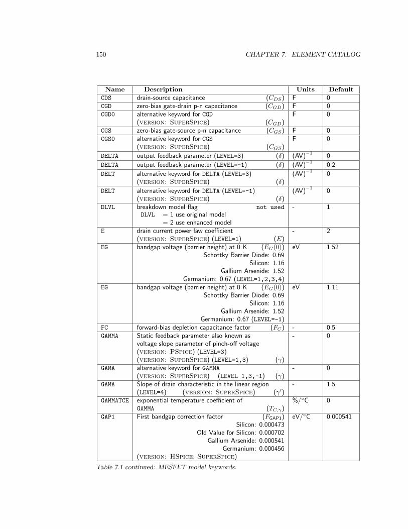
150 CHAPTER 7. ELEMENT CATALOG
Name Description Units DefaultCDS drain-source capacitance (CDS) F 0CGD zero-bias gate-drain p-n capacitance (CGD) F 0CGD0 alternative keyword for CGD
(version: SuperSpice) (CGD)F 0
CGS zero-bias gate-source p-n capacitance (CGS) F 0CGS0 alternative keyword for CGS
(version: SuperSpice) (CGS)F 0
DELTA output feedback parameter (LEVEL=3) (δ) (AV)−1 0
DELTA output feedback parameter (LEVEL=-1) (δ) (AV)−1 0.2
DELT alternative keyword for DELTA (LEVEL=3)(version: SuperSpice) (δ)
(AV)−1 0
DELT alternative keyword for DELTA (LEVEL=-1)(version: SuperSpice) (δ)
(AV)−1 0
DLVL breakdown model flag not usedDLVL = 1 use original model
= 2 use enhanced model
- 1
E drain current power law coefficient(version: SuperSpice) (LEVEL=1) (E)
- 2
EG bandgap voltage (barrier height) at 0 K (EG(0))Schottky Barrier Diode: 0.69
Silicon: 1.16Gallium Arsenide: 1.52
Germanium: 0.67 (LEVEL=1,2,3,4)
eV 1.52
EG bandgap voltage (barrier height) at 0 K (EG(0))Schottky Barrier Diode: 0.69
Silicon: 1.16Gallium Arsenide: 1.52
Germanium: 0.67 (LEVEL=-1)
eV 1.11
FC forward-bias depletion capacitance factor (FC) - 0.5GAMMA Static feedback parameter also known as
voltage slope parameter of pinch-off voltage(version: PSpice) (LEVEL=3)(version: SuperSpice) (LEVEL=1,3) (γ)
- 0
GAMA alternative keyword for GAMMA(version: SuperSpice) (LEVEL 1,3,-1) (γ)
- 0
GAMA Slope of drain characteristic in the linear region(LEVEL=4) (version: SuperSpice) (γ′)
- 1.5
GAMMATCE exponential temperature coefficient ofGAMMA (TC,γ)
%/C 0
GAP1 First bandgap correction factor (FGAP1)Silicon: 0.000473
Old Value for Silicon: 0.000702Gallium Arsenide: 0.000541
Germanium: 0.000456(version: HSpice; SuperSpice)
eV/C 0.000541
Table 7.1 continued: MESFET model keywords.
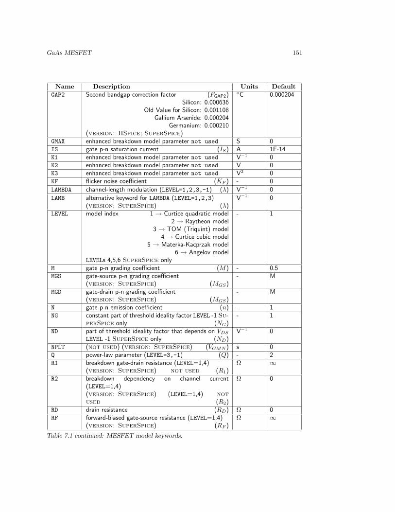
GaAs MESFET 151
Name Description Units DefaultGAP2 Second bandgap correction factor (FGAP2)
Silicon: 0.000636Old Value for Silicon: 0.001108
Gallium Arsenide: 0.000204Germanium: 0.000210
(version: HSpice; SuperSpice)
C 0.000204
GMAX enhanced breakdown model parameter not used S 0IS gate p-n saturation current (IS) A 1E-14K1 enhanced breakdown model parameter not used V−1 0K2 enhanced breakdown model parameter not used V 0K3 enhanced breakdown model parameter not used V2 0KF flicker noise coefficient (KF ) - 0
LAMBDA channel-length modulation (LEVEL=1,2,3,-1) (λ) V−1 0
LAMB alternative keyword for LAMBDA (LEVEL=1,2,3)(version: SuperSpice) (λ)
V−1 0
LEVEL model index 1 → Curtice quadratic model2 → Raytheon model
3 → TOM (Triquint) model4 → Curtice cubic model
5 → Materka-Kacprzak model6 → Angelov model
LEVELs 4,5,6 SuperSpice only
- 1
M gate p-n grading coefficient (M) - 0.5MGS gate-source p-n grading coefficient
(version: SuperSpice) (MGS)- M
MGD gate-drain p-n grading coefficient(version: SuperSpice) (MGS)
- M
N gate p-n emission coefficient (n) - 1NG constant part of threshold ideality factor LEVEL -1 Su-
perSpice only (NG)- 1
ND part of threshold ideality factor that depends on VDS
LEVEL -1 SuperSpice only (ND)V−1 0
NPLT (not used) (version: SuperSpice) (VGMN ) s 0Q power-law parameter (LEVEL=3,-1) (Q) - 2R1 breakdown gate-drain resistance (LEVEL=1,4)
(version: SuperSpice) not used (R1)Ω ∞
R2 breakdown dependency on channel current(LEVEL=1,4)(version: SuperSpice) (LEVEL=1,4) notused (R2)
Ω 0
RD drain resistance (RD) Ω 0RF forward-biased gate-source resistance (LEVEL=1,4)
(version: SuperSpice) (RF )Ω ∞
Table 7.1 continued: MESFET model keywords.

152 CHAPTER 7. ELEMENT CATALOG
Name Description Units DefaultRG gate resistance (RG) Ω 0RI channel resistance (not used)
(version: SuperSpice) (RI)Ω 0
RS source resistance (RS) Ω 0T alternative keyword for TAU
(version: SuperSpice) (τ)s 0
TBET alternative keyword for BETATCE(version: SuperSpice) (TC,β)
s 0
TJ junction temperature (not used)(version: SuperSpice) (TJ)
s 0
TM (not used) (version: SuperSpice) (TM ) s 0TME (not used) (version: SuperSpice) (TME) s 0TNOM nominal temperature (not used)
(version: SuperSpice) (TNOM)s 0
TAU conduction current delay time (τ) s 0
TRG1 linear temperature coefficient of RG (ARG) C−1 0
TRD1 linear temperature coefficient of RD (ARD) C−1 0
TRS1 linear temperature coefficient of RS (ARS) C−1 0U critical field parameter for mobility degradation
(LEVEL=1,2,3)(version: SuperSpice) (U)
V/m 0
VBI gate p-n potential (VBI) V 1VBR enhanced breakdown model parameter not used V2 ∞VBD breakdown voltage
(version: SuperSpice) (AV BD))V ∞
VDELTA capacitance transistion voltage(LEVEL=2,3) (V∆)
V 0.2
VDS0 VDS at which BETA was measured(LEVEL=4) (version: SuperSpice) (V∆)
V 4
VGMN (not used) (version: SuperSpice) (VGMN ) s 0VGMX (not used) (version: SuperSpice) (VGMN ) s 0VDMX (not used) (version: SuperSpice) (VGMN ) s 0VMAX capacitance limiting voltage
(LEVEL=2,3) (VMAX)V 0.5
VTO (VT-oh) pinch-off voltage (VT0) V -2.5VT0 (VT-0) alternative keyword for VTO
(version: SuperSpice) (AV DS0))V -2.5
VTOTC linear temperature coefficient of VTO (TC,V T0) V/C 0XTI temperature exponent of IS (XTI) - 0VBITC linear temperature coefficient of VBI (TC,BI) - 0
Some versions of Spice use incorrect default values for some of the parameters. Oneexample is the default value for EG. The accepted value has changed with time. It is alwaysa good idea not to rely on default values other than 0. The physical constants used in themodel evaluation are
k Boltzmann’s constant 1.3806226 10−23 J/Kq electronic charge 1.6021918 10−19 C
Standard Calculations

GaAs MESFET 153
Absolute temperatures (in kelvins, K) are used. The thermal voltage VTH = kT/q and theband gap energy at the nominal temperature is
EG(TNOM) = EG(0)− FGAP14T 2NOM/ (TNOM + FGAP2). (7.1)
Here EG(0) is the parameter EG — the band gap energy at 0 K. FGAP1 and FGAP2 arenot parameters in PSpice. PSpice documentation indicates that PSpice uses FGAP1 =0.000702 and FGAP2 = 1108.
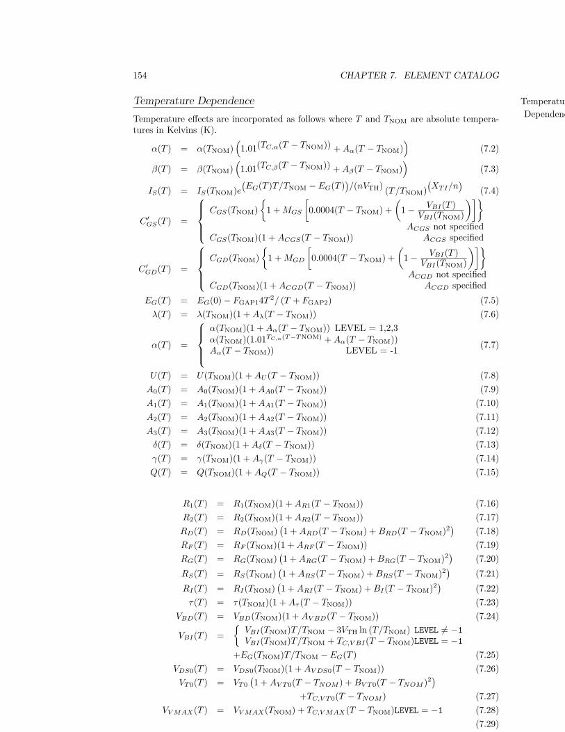
154 CHAPTER 7. ELEMENT CATALOG
Temperature Dependence TemperatureDependenceTemperature effects are incorporated as follows where T and TNOM are absolute tempera-
tures in Kelvins (K).
α(T ) = α(TNOM)(1.01(TC,α(T − TNOM)) + Aα(T − TNOM)
)(7.2)
β(T ) = β(TNOM)(1.01(TC,β(T − TNOM)) + Aβ(T − TNOM)
)(7.3)
IS(T ) = IS(TNOM)e(EG(T )T/TNOM − EG(T )
)/(nVTH) (T/TNOM)
(XTI/n
)(7.4)
C ′GS(T ) =
CGS(TNOM)
1 + MGS
[0.0004(T − TNOM) +
(1− VBI(T )
VBI(TNOM)
)]
ACGS not specifiedCGS(TNOM)(1 + ACGS(T − TNOM)) ACGS specified
C ′GD(T ) =
CGD(TNOM)
1 + MGD
[0.0004(T − TNOM) +
(1− VBI(T )
VBI(TNOM)
)]
ACGD not specifiedCGD(TNOM)(1 + ACGD(T − TNOM)) ACGD specified
EG(T ) = EG(0)− FGAP14T 2/ (T + FGAP2) (7.5)λ(T ) = λ(TNOM)(1 + Aλ(T − TNOM)) (7.6)
α(T ) =
α(TNOM)(1 + Aα(T − TNOM)) LEVEL = 1,2,3α(TNOM)(1.01TC,α(T−TNOM) + Aα(T − TNOM))Aα(T − TNOM)) LEVEL = -1
(7.7)
U(T ) = U(TNOM)(1 + AU (T − TNOM)) (7.8)A0(T ) = A0(TNOM)(1 + AA0(T − TNOM)) (7.9)A1(T ) = A1(TNOM)(1 + AA1(T − TNOM)) (7.10)A2(T ) = A2(TNOM)(1 + AA2(T − TNOM)) (7.11)A3(T ) = A3(TNOM)(1 + AA3(T − TNOM)) (7.12)
δ(T ) = δ(TNOM)(1 + Aδ(T − TNOM)) (7.13)γ(T ) = γ(TNOM)(1 + Aγ(T − TNOM)) (7.14)Q(T ) = Q(TNOM)(1 + AQ(T − TNOM)) (7.15)
R1(T ) = R1(TNOM)(1 + AR1(T − TNOM)) (7.16)R2(T ) = R2(TNOM)(1 + AR2(T − TNOM)) (7.17)RD(T ) = RD(TNOM)
(1 + ARD(T − TNOM) + BRD(T − TNOM)2
)(7.18)
RF (T ) = RF (TNOM)(1 + ARF (T − TNOM)) (7.19)RG(T ) = RG(TNOM)
(1 + ARG(T − TNOM) + BRG(T − TNOM)2
)(7.20)
RS(T ) = RS(TNOM)(1 + ARS(T − TNOM) + BRS(T − TNOM)2
)(7.21)
RI(T ) = RI(TNOM)(1 + ARI(T − TNOM) + BI(T − TNOM)2
)(7.22)
τ(T ) = τ(TNOM)(1 + Aτ (T − TNOM)) (7.23)VBD(T ) = VBD(TNOM)(1 + AV BD(T − TNOM)) (7.24)
VBI(T ) =
VBI(TNOM)T/TNOM − 3VTH ln (T/TNOM) LEVEL 6= −1VBI(TNOM)T/TNOM + TC,V BI(T − TNOM)LEVEL = −1
+EG(TNOM)T/TNOM − EG(T ) (7.25)VDS0(T ) = VDS0(TNOM)(1 + AV DS0(T − TNOM)) (7.26)VT0(T ) = VT0
(1 + AV T0(T − TNOM ) + BV T0(T − TNOM )2
)
+TC,V T0(T − TNOM ) (7.27)VV MAX(T ) = VV MAX(TNOM) + TC,V MAX(T − TNOM)LEVEL = −1 (7.28)
(7.29)
Parasitic Resistances
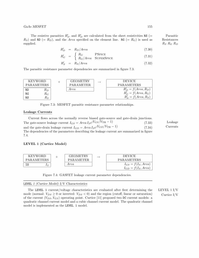
GaAs MESFET 155
The resistive parasitics R′S , and R′D are calculated from the sheet resistivities RS (= ParasiticResistancesRS RG RD
RS) and RD (= RD), and the Area specified on the element line. RG (= RG) is used assupplied.
R′D = RD/Area (7.30)
R′G =
RG PSpiceRG/Area SuperSpice
(7.31)
R′S = RS/Area (7.32)
The parasitic resistance parameter dependencies are summarized in figure 7.3.
KEYWORDPARAMETERSRD RD
RG RG
RS RS
+ GEOMETRYPARAMETERArea
→ DEVICEPARAMETERS
R′D = f(Area,RD)R′G = f(Area, RG)R′S = f(Area, RS)
Figure 7.3: MESFET parasitic resistance parameter relationships.
Leakage Currents
Current flows across the normally reverse biased gate-source and gate-drain junctions.LeakageCurrents
The gate-source leakage current IGS = Area ISe(VGS/VTH − 1) (7.33)and the gate-drain leakage current IGD = Area ISe(VGD/VTH − 1) (7.34)The dependencies of the parameters describing the leakage current are summarized in figure7.4.
LEVEL 1 (Curtice Model)
KEYWORDPARAMETERSIS IS
+ GEOMETRYPARAMETERArea
→ DEVICEPARAMETERS
IGS = f(IS , Area)IGD = f(IS , Area)
Figure 7.4: GASFET leakage current parameter dependencies.
LEVEL 1 (Curtice Model) I/V Characteristics
The LEVEL 1 current/voltage characteristics are evaluated after first determining the LEVEL 1 I/VCurtice I/Vmode (normal: VDS ≥ 0 or inverted: VDS < 0) and the region (cutoff, linear or saturation)
of the current (VDS , VGS) operating point. Curtice [11] proposed two DC current models: aquadratic channel current model and a cubic channel current model. The quadratic channelmodel is implemented as the LEVEL 1 model.
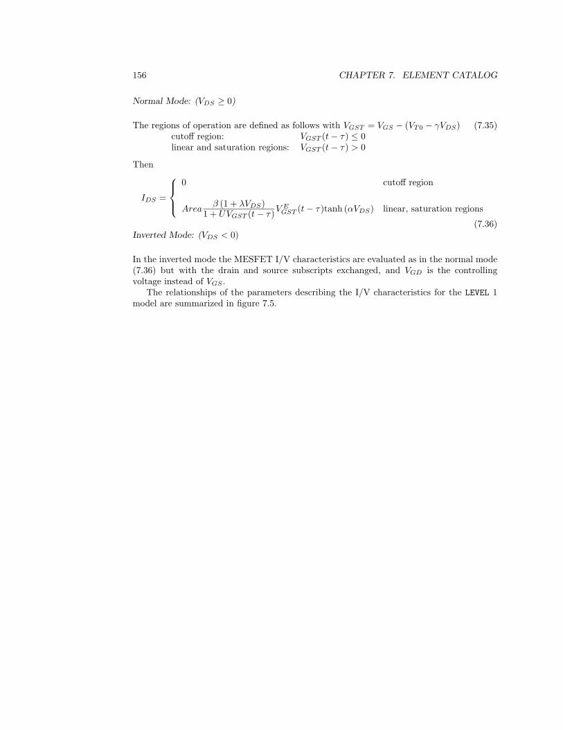
156 CHAPTER 7. ELEMENT CATALOG
Normal Mode: (VDS ≥ 0)
The regions of operation are defined as follows with VGST = VGS − (VT0 − γVDS) (7.35)cutoff region: VGST (t− τ) ≤ 0linear and saturation regions: VGST (t− τ) > 0
Then
IDS =
0 cutoff region
Areaβ (1 + λVDS)
1 + UVGST (t− τ)V EGST (t− τ)tanh (αVDS) linear, saturation regions
(7.36)Inverted Mode: (VDS < 0)
In the inverted mode the MESFET I/V characteristics are evaluated as in the normal mode(7.36) but with the drain and source subscripts exchanged, and VGD is the controllingvoltage instead of VGS .
The relationships of the parameters describing the I/V characteristics for the LEVEL 1model are summarized in figure 7.5.
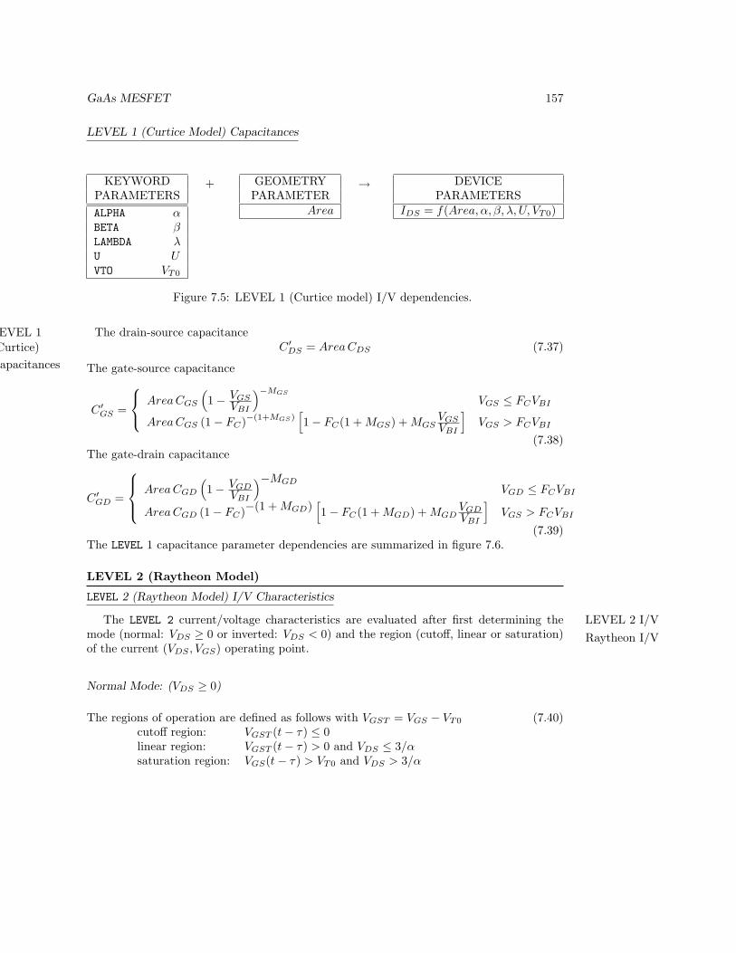
GaAs MESFET 157
LEVEL 1 (Curtice Model) Capacitances
KEYWORDPARAMETERSALPHA αBETA βLAMBDA λU UVTO VT0
+ GEOMETRYPARAMETER
Area
→ DEVICEPARAMETERS
IDS = f(Area, α, β, λ, U, VT0)
Figure 7.5: LEVEL 1 (Curtice model) I/V dependencies.
The drain-source capacitanceLEVEL 1(Curtice)Capacitances
C ′DS = AreaCDS (7.37)
The gate-source capacitance
C ′GS =
AreaCGS
(1− VGS
VBI
)−MGS
VGS ≤ FCVBI
AreaCGS (1− FC)−(1+MGS)[1− FC(1 + MGS) + MGS
VGSVBI
]VGS > FCVBI
(7.38)The gate-drain capacitance
C ′GD =
Area CGD
(1− VGD
VBI
)−MGDVGD ≤ FCVBI
Area CGD (1− FC)−(1 + MGD) [1− FC(1 + MGD) + MGD
VGDVBI
]VGS > FCVBI
(7.39)The LEVEL 1 capacitance parameter dependencies are summarized in figure 7.6.
LEVEL 2 (Raytheon Model)
LEVEL 2 (Raytheon Model) I/V Characteristics
The LEVEL 2 current/voltage characteristics are evaluated after first determining the LEVEL 2 I/VRaytheon I/Vmode (normal: VDS ≥ 0 or inverted: VDS < 0) and the region (cutoff, linear or saturation)
of the current (VDS , VGS) operating point.
Normal Mode: (VDS ≥ 0)
The regions of operation are defined as follows with VGST = VGS − VT0 (7.40)cutoff region: VGST (t− τ) ≤ 0linear region: VGST (t− τ) > 0 and VDS ≤ 3/αsaturation region: VGS(t− τ) > VT0 and VDS > 3/α

158 CHAPTER 7. ELEMENT CATALOG
KEYWORDPARAMETERSCGD CGD
CGS CGS
CDS CDS
FC FC
VBI VBI
MGS MGS
MGD MGD
+ GEOMETRYPARAMETER
Area
→ DEVICEPARAMETERS
C ′DS = f(Area, CDS)C ′GD =f(Area, CGD, FC , VBI ,MGD)C ′GS =f(Area, CGS , FC , VBI ,MGS)
Figure 7.6: LEVEL 1 (Curtice model) capacitance dependencies.
Then
IDS =
0 cutoff region
Areaβ
1 + UVGST(1 + λVDS) VGST (t− τ)2
1 + BVGST (t− τ)Ktanh linear and saturation
regions(7.41)
where
Ktanh =
1−(1− VDS
α3
)3
linear region
1 saturation regions
(7.42)
is a Taylor series approximation to the tanh function of the LEVEL 1 model.
Inverted Mode: (VDS < 0)
In the inverted mode the MESFET I/V characteristics are evaluated as in the normal mode(7.41) but with the drain and source subscripts exchanged, and VGD is the controllingvoltage instead of VGS .
The relationships of the parameters describing the I/V characteristics of the LEVEL 2model are summarized in figure 7.7.
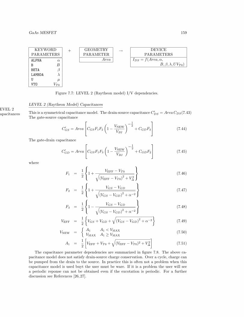
GaAs MESFET 159
KEYWORDPARAMETERSALPHA αB BBETA βLAMBDA λU µVTO VT0
+ GEOMETRYPARAMETER
Area
→ DEVICEPARAMETERS
IDS = f(Area, α,B, β, λ, UVT0)
Figure 7.7: LEVEL 2 (Raytheon model) I/V dependencies.
LEVEL 2 (Raytheon Model) CapacitancesLEVEL 2Capacitances This is a symmetrical capacitance model. The drain-source capacitance C ′DS = Area CDS(7.43)
The gate-source capacitance
C ′GS = Area
CGSF1F2
(1− VNEW
VBI
)− 12
+ CGDF3
(7.44)
The gate-drain capacitance
C ′GD = Area
CGSF1F3
(1− VNEW
VBI
)− 12
+ CGDF2
(7.45)
where
F1 =12
1 +
VEFF − VT0√(VEFF − VT0)
2 + V 2∆
(7.46)
F2 =12
1 +
VGS − VGD√(VGS − VGD)2 + α−2
(7.47)
F3 =12
1− VGS − VGD√
(VGS − VGD)2 + α−2
(7.48)
VEFF =12
VGS + VGD +
√(VGS − VGD)2 + α−2
(7.49)
VNEW =
A1 A1 < VMAX
VMAX A1 ≥ VMAX(7.50)
A1 =12
[VEFF + VT0 +
√(VEFF − VT0)2 + V 2
∆
](7.51)
The capacitance parameter dependencies are summarized in figure 7.8. The above ca-pacitance model does not satisfy drain-source charge conservation. Over a cycle, charge canbe pumped from the drain to the source. In practice this is often not a problem when thiscapacitance model is used buyt the user must be ware. If it is a problem the user will seea periodic reponse can not be obtained even if the excotation is periodic. For a furtherdiscussion see References [26,27].
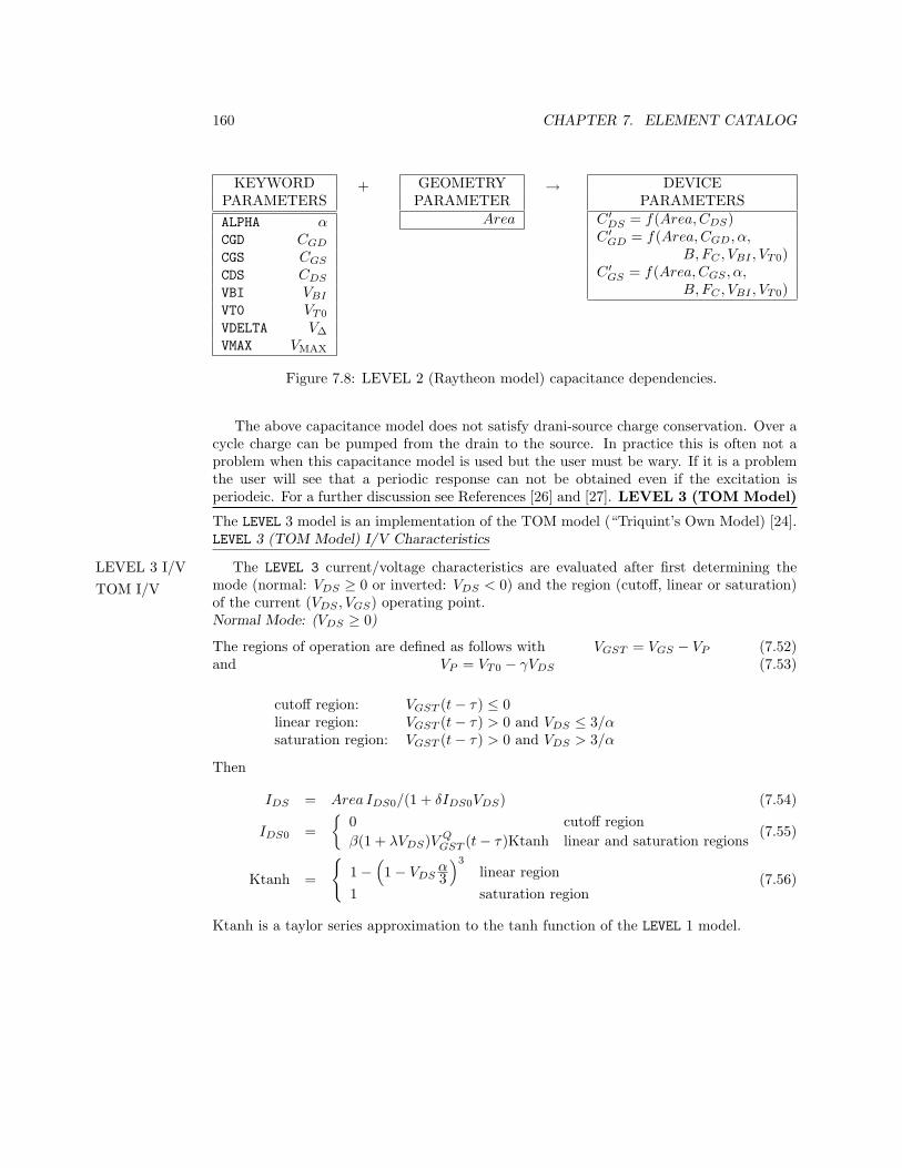
160 CHAPTER 7. ELEMENT CATALOG
KEYWORDPARAMETERSALPHA αCGD CGD
CGS CGS
CDS CDS
VBI VBI
VT0 VT0
VDELTA V∆
VMAX VMAX
+ GEOMETRYPARAMETER
Area
→ DEVICEPARAMETERS
C ′DS = f(Area, CDS)C ′GD = f(Area,CGD, α,
B, FC , VBI , VT0)C ′GS = f(Area, CGS , α,
B, FC , VBI , VT0)
Figure 7.8: LEVEL 2 (Raytheon model) capacitance dependencies.
The above capacitance model does not satisfy drani-source charge conservation. Over acycle charge can be pumped from the drain to the source. In practice this is often not aproblem when this capacitance model is used but the user must be wary. If it is a problemthe user will see that a periodic response can not be obtained even if the excitation isperiodeic. For a further discussion see References [26] and [27]. LEVEL 3 (TOM Model)
The LEVEL 3 model is an implementation of the TOM model (“Triquint’s Own Model) [24].LEVEL 3 (TOM Model) I/V Characteristics
The LEVEL 3 current/voltage characteristics are evaluated after first determining theLEVEL 3 I/VTOM I/V mode (normal: VDS ≥ 0 or inverted: VDS < 0) and the region (cutoff, linear or saturation)
of the current (VDS , VGS) operating point.Normal Mode: (VDS ≥ 0)
The regions of operation are defined as follows with VGST = VGS − VP (7.52)and VP = VT0 − γVDS (7.53)
cutoff region: VGST (t− τ) ≤ 0linear region: VGST (t− τ) > 0 and VDS ≤ 3/αsaturation region: VGST (t− τ) > 0 and VDS > 3/α
Then
IDS = Area IDS0/(1 + δIDS0VDS) (7.54)
IDS0 =
0 cutoff regionβ(1 + λVDS)V Q
GST (t− τ)Ktanh linear and saturation regions(7.55)
Ktanh =
1−
(1− VDS
α3
)3
linear region1 saturation region
(7.56)
Ktanh is a taylor series approximation to the tanh function of the LEVEL 1 model.
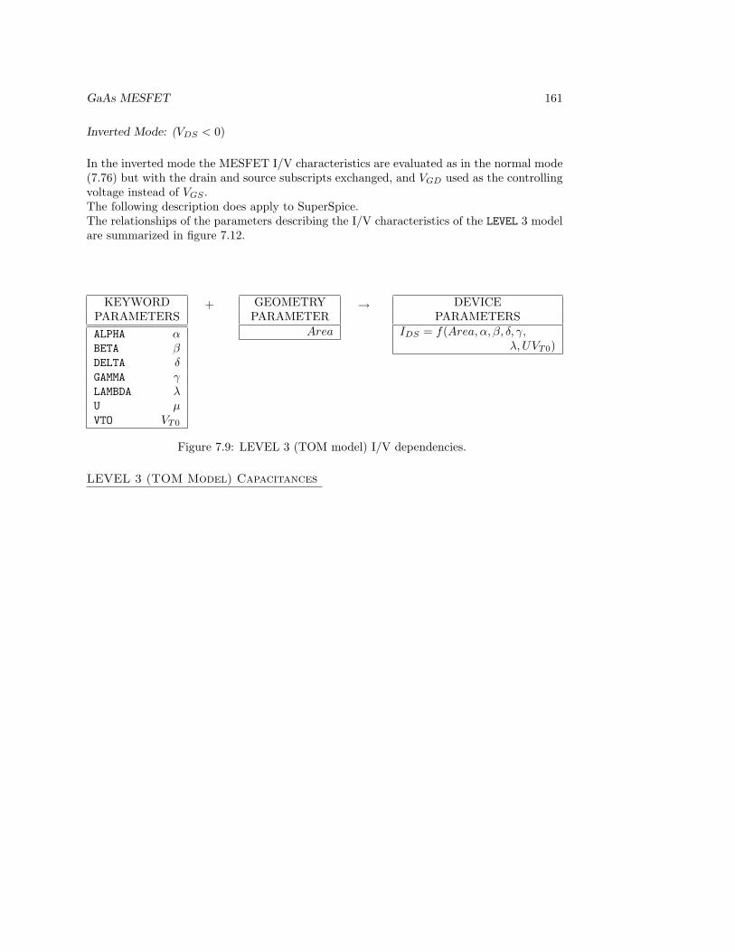
GaAs MESFET 161
Inverted Mode: (VDS < 0)
In the inverted mode the MESFET I/V characteristics are evaluated as in the normal mode(7.76) but with the drain and source subscripts exchanged, and VGD used as the controllingvoltage instead of VGS .The following description does apply to SuperSpice.The relationships of the parameters describing the I/V characteristics of the LEVEL 3 modelare summarized in figure 7.12.
KEYWORDPARAMETERSALPHA αBETA βDELTA δGAMMA γLAMBDA λU µVTO VT0
+ GEOMETRYPARAMETER
Area
→ DEVICEPARAMETERS
IDS = f(Area, α, β, δ, γ,λ, UVT0)
Figure 7.9: LEVEL 3 (TOM model) I/V dependencies.
LEVEL 3 (TOM Model) Capacitances
162 CHAPTER 7. ELEMENT CATALOG
The drain-source capacitance C ′DS = Area CDS (7.57)The gate-source capacitance
C ′GS = Area
CGSF1F2
(1− VNEW
VBI
)− 12
+ CGDF3
(7.58)
The gate-drain capacitance is given by
C ′GD = Area
CGSF1F3
(1− VNEW
VBI
)− 12
+ CGDF2
(7.59)
F1 =12
1 +
VEFF − VP√(VEFF − VT0)
2 + V 2∆
(7.60)
F2 =12
1 +
VGS − VGD√(VGS − VGD)2 + α−2
(7.61)
F3 =12
1− VGS − VGD√
(VGS − VGD)2 + α−2
(7.62)
VEFF =12
VGS + VGD +
√(VGS − VGD)2 + α−2
(7.63)
VNEW =
A1 A1 < VMAX
VMAX A1 ≥ VMAX(7.64)
and A1 = 12
[VEFF + VP +
√(VEFF − VP )2 + V 2
∆
](7.65)
The capacitance parameter dependencies are summarized in figure 7.13.
LEVEL -1 (TOM-2 Model)LEVEL -1 The LEVEL -1 model is an enhancement of the LEVEL 3 TOM model.
LEVEL -1 (TOM Model) I/V Characteristics
The LEVEL -1 current/voltage characteristics are evaluated after first determining theLEVEL -1 I/VTOM-2 I/V mode (normal: VDS ≥ 0 or inverted: VDS < 0) and the region (cutoff, linear or saturation)
of the current (VDS , VGS) operating point.Normal Mode: (VDS ≥ 0)
The regions of operation are defined as follows with VGST = VGS − VP (7.66)and VP = VT0 − γVDS (7.67)
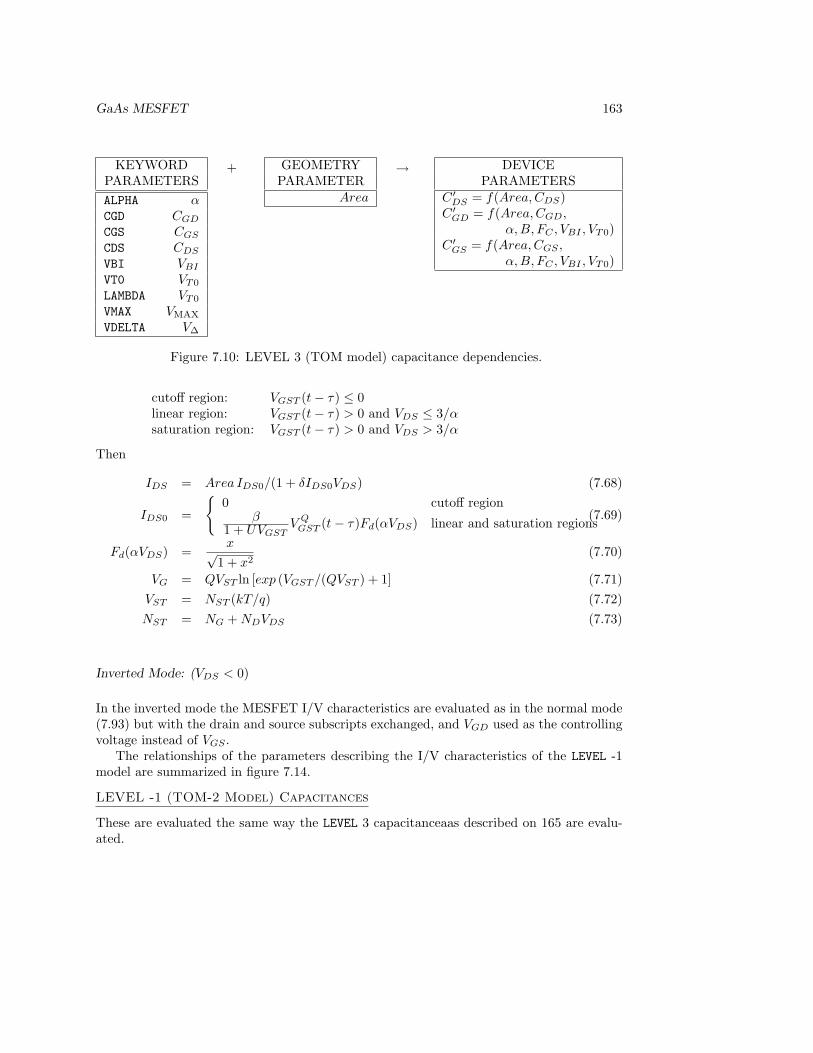
GaAs MESFET 163
KEYWORDPARAMETERSALPHA αCGD CGD
CGS CGS
CDS CDS
VBI VBI
VT0 VT0
LAMBDA VT0
VMAX VMAX
VDELTA V∆
+ GEOMETRYPARAMETER
Area
→ DEVICEPARAMETERS
C ′DS = f(Area, CDS)C ′GD = f(Area,CGD,
α, B, FC , VBI , VT0)C ′GS = f(Area, CGS ,
α, B, FC , VBI , VT0)
Figure 7.10: LEVEL 3 (TOM model) capacitance dependencies.
cutoff region: VGST (t− τ) ≤ 0linear region: VGST (t− τ) > 0 and VDS ≤ 3/αsaturation region: VGST (t− τ) > 0 and VDS > 3/α
Then
IDS = Area IDS0/(1 + δIDS0VDS) (7.68)
IDS0 =
0 cutoff region
β1 + UVGST
V QGST (t− τ)Fd(αVDS) linear and saturation regions
(7.69)
Fd(αVDS) =x√
1 + x2(7.70)
VG = QVST ln [exp (VGST /(QVST ) + 1] (7.71)VST = NST (kT/q) (7.72)NST = NG + NDVDS (7.73)
Inverted Mode: (VDS < 0)
In the inverted mode the MESFET I/V characteristics are evaluated as in the normal mode(7.93) but with the drain and source subscripts exchanged, and VGD used as the controllingvoltage instead of VGS .
The relationships of the parameters describing the I/V characteristics of the LEVEL -1model are summarized in figure 7.14.
LEVEL -1 (TOM-2 Model) Capacitances
These are evaluated the same way the LEVEL 3 capacitanceaas described on 165 are evalu-ated.
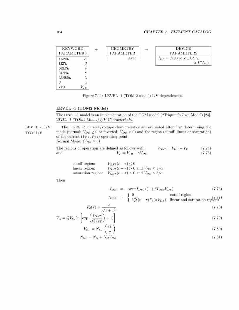
164 CHAPTER 7. ELEMENT CATALOG
KEYWORDPARAMETERSALPHA αBETA βDELTA δGAMMA γLAMBDA λU µVTO VT0
+ GEOMETRYPARAMETER
Area
→ DEVICEPARAMETERS
IDS = f(Area, α, β, δ, γ,λ, UVT0)
Figure 7.11: LEVEL -1 (TOM-2 model) I/V dependencies.
LEVEL -1 (TOM2 Model)
The LEVEL -1 model is an implementation of the TOM model (“Triquint’s Own Model) [24].LEVEL -1 (TOM2 Model) I/V Characteristics
The LEVEL -1 current/voltage characteristics are evaluated after first determining theLEVEL -1 I/VTOM I/V mode (normal: VDS ≥ 0 or inverted: VDS < 0) and the region (cutoff, linear or saturation)
of the current (VDS , VGS) operating point.Normal Mode: (VDS ≥ 0)
The regions of operation are defined as follows with VGST = VGS − VP (7.74)and VP = VT0 − γVDS (7.75)
cutoff region: VGST (t− τ) ≤ 0linear region: VGST (t− τ) > 0 and VDS ≤ 3/αsaturation region: VGST (t− τ) > 0 and VDS > 3/α
Then
IDS = Area IDS0/(1 + δIDS0VDS) (7.76)
IDS0 =
0 cutoff regionV Q
G (t− τ)Fd(αVDS) linear and saturation regions(7.77)
Fd(x) =x√
1 + x2(7.78)
VG = QVST ln[exp
(VGST
QVST
)+ 1)
](7.79)
VST = NST
(kT
q
)(7.80)
NST = NG + NDVDS (7.81)
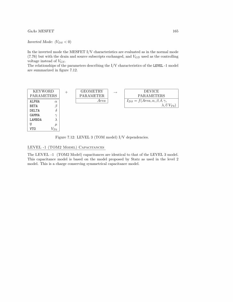
GaAs MESFET 165
Inverted Mode: (VDS < 0)
In the inverted mode the MESFET I/V characteristics are evaluated as in the normal mode(7.76) but with the drain and source subscripts exchanged, and VGD used as the controllingvoltage instead of VGS .The relationships of the parameters describing the I/V characteristics of the LEVEL -1 modelare summarized in figure 7.12.
KEYWORDPARAMETERSALPHA αBETA βDELTA δGAMMA γLAMBDA λU µVTO VT0
+ GEOMETRYPARAMETER
Area
→ DEVICEPARAMETERS
IDS = f(Area, α, β, δ, γ,λ, UVT0)
Figure 7.12: LEVEL 3 (TOM model) I/V dependencies.
LEVEL -1 (TOM2 Model) Capacitances
The LEVEL -1 (TOM2 Model) capacitances are identical to that of the LEVEL 3 model.This capacitance model is based on the model proposed by Statz as used in the level 2model. This is a charge conserving symmetrical capacitance model.
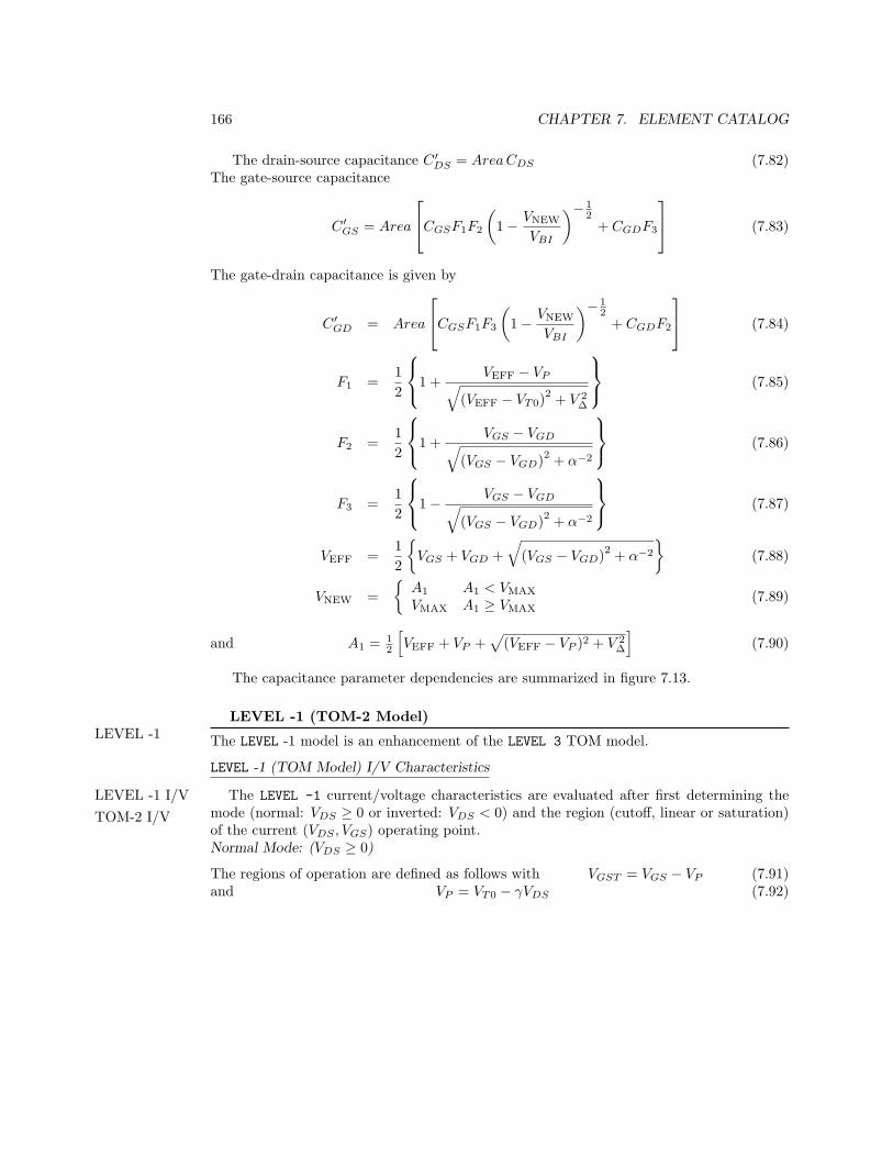
166 CHAPTER 7. ELEMENT CATALOG
The drain-source capacitance C ′DS = Area CDS (7.82)The gate-source capacitance
C ′GS = Area
CGSF1F2
(1− VNEW
VBI
)− 12
+ CGDF3
(7.83)
The gate-drain capacitance is given by
C ′GD = Area
CGSF1F3
(1− VNEW
VBI
)− 12
+ CGDF2
(7.84)
F1 =12
1 +
VEFF − VP√(VEFF − VT0)
2 + V 2∆
(7.85)
F2 =12
1 +
VGS − VGD√(VGS − VGD)2 + α−2
(7.86)
F3 =12
1− VGS − VGD√
(VGS − VGD)2 + α−2
(7.87)
VEFF =12
VGS + VGD +
√(VGS − VGD)2 + α−2
(7.88)
VNEW =
A1 A1 < VMAX
VMAX A1 ≥ VMAX(7.89)
and A1 = 12
[VEFF + VP +
√(VEFF − VP )2 + V 2
∆
](7.90)
The capacitance parameter dependencies are summarized in figure 7.13.
LEVEL -1 (TOM-2 Model)LEVEL -1 The LEVEL -1 model is an enhancement of the LEVEL 3 TOM model.
LEVEL -1 (TOM Model) I/V Characteristics
The LEVEL -1 current/voltage characteristics are evaluated after first determining theLEVEL -1 I/VTOM-2 I/V mode (normal: VDS ≥ 0 or inverted: VDS < 0) and the region (cutoff, linear or saturation)
of the current (VDS , VGS) operating point.Normal Mode: (VDS ≥ 0)
The regions of operation are defined as follows with VGST = VGS − VP (7.91)and VP = VT0 − γVDS (7.92)

GaAs MESFET 167
KEYWORDPARAMETERSALPHA αCGD CGD
CGS CGS
CDS CDS
VBI VBI
VT0 VT0
LAMBDA VT0
VMAX VMAX
VDELTA V∆
+ GEOMETRYPARAMETER
Area
→ DEVICEPARAMETERS
C ′DS = f(Area, CDS)C ′GD = f(Area,CGD,
α, B, FC , VBI , VT0)C ′GS = f(Area, CGS ,
α, B, FC , VBI , VT0)
Figure 7.13: LEVEL 3 (TOM model) capacitance dependencies.
cutoff region: VGST (t− τ) ≤ 0linear region: VGST (t− τ) > 0 and VDS ≤ 3/αsaturation region: VGST (t− τ) > 0 and VDS > 3/α
Then
IDS = Area IDS0/(1 + δIDS0VDS) (7.93)
IDS0 =
0 cutoff region
β1 + UVGST
V QGST (t− τ)Fd(αVDS) linear and saturation regions
(7.94)
Fd(αVDS) =x√
1 + x2(7.95)
VG = QVST ln [exp (VGST /(QVST ) + 1] (7.96)VST = NST (kT/q) (7.97)NST = NG + NDVDS (7.98)
Inverted Mode: (VDS < 0)
In the inverted mode the MESFET I/V characteristics are evaluated as in the normal mode(7.93) but with the drain and source subscripts exchanged, and VGD used as the controllingvoltage instead of VGS .
The relationships of the parameters describing the I/V characteristics of the LEVEL -1model are summarized in figure 7.14.
LEVEL -1 (TOM-2 Model) Capacitances
These are evaluated the same way the LEVEL 3 capacitanceaas described on 165 are evalu-ated.
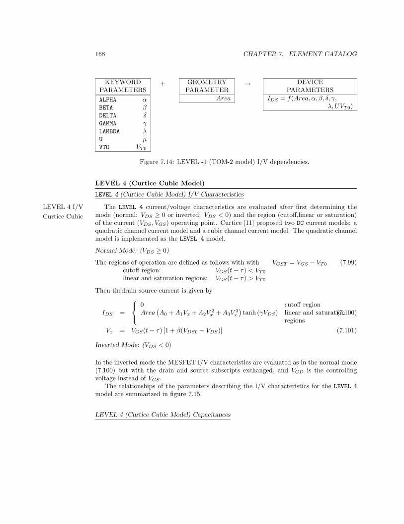
168 CHAPTER 7. ELEMENT CATALOG
KEYWORDPARAMETERSALPHA αBETA βDELTA δGAMMA γLAMBDA λU µVTO VT0
+ GEOMETRYPARAMETER
Area
→ DEVICEPARAMETERS
IDS = f(Area, α, β, δ, γ,λ, UVT0)
Figure 7.14: LEVEL -1 (TOM-2 model) I/V dependencies.
LEVEL 4 (Curtice Cubic Model)
LEVEL 4 (Curtice Cubic Model) I/V Characteristics
The LEVEL 4 current/voltage characteristics are evaluated after first determining theLEVEL 4 I/VCurtice Cubic mode (normal: VDS ≥ 0 or inverted: VDS < 0) and the region (cutoff,linear or saturation)
of the current (VDS , VGS) operating point. Curtice [11] proposed two DC current models: aquadratic channel current model and a cubic channel current model. The quadratic channelmodel is implemented as the LEVEL 4 model.
Normal Mode: (VDS ≥ 0)
The regions of operation are defined as follows with with VGST = VGS − VT0 (7.99)cutoff region: VGS(t− τ) < VT0
linear and saturation regions: VGS(t− τ) > VT0
Then thedrain source current is given by
IDS =
0 cutoff regionArea
(A0 + A1Vx + A2V
2x + A3V
3x
)tanh (γVDS) linear and saturation
regions(7.100)
Vx = VGS(t− τ) [1 + β(VDS0 − VDS)] (7.101)
Inverted Mode: (VDS < 0)
In the inverted mode the MESFET I/V characteristics are evaluated as in the normal mode(7.100) but with the drain and source subscripts exchanged, and VGD is the controllingvoltage instead of VGS .
The relationships of the parameters describing the I/V characteristics for the LEVEL 4model are summarized in figure 7.15.
LEVEL 4 (Curtice Cubic Model) Capacitances

GaAs MESFET 169
KEYWORDPARAMETERSA0 A0
A1 A1
A2 A2
A3 A3
BETA βGAMMA γT, TAU τVTO VT0
+ GEOMETRYPARAMETER
Area
→ DEVICEPARAMETERS
IDS = f(Area,A0, A1, A2, A3, β, γ, VT0)
Figure 7.15: LEVEL 4 (Curtice cubic model) I/V dependencies.
The drain-source capacitance C ′DS = Area CDS (7.102) LEVEL 4Curtice
CubicCapacitances
the gate-source and gate-drain capacitances are
C ′GS =
AreaCGS
(1− VGS
VBI
)−MGSVGS ≤ FCVBI
AreaCGS (1− FC)−(1 + MGS) [1− FC(1 + MGS) + MGS
VGSVBI
]VGS > FCVBI
(7.103)
CGD =
AreaCGD
(1− VGD
VBI
)−MGDVGD ≤ FCVBI
AreaCGD (1− FC)−(1 + MGD) [1− FC(1 + MGD) + MGD
VGDVBI
]VGS > FCVBI
(7.104)
The LEVEL 4 capacitance parameter dependencies are summarized in figure 7.16.
KEYWORDPARAMETERSCGD CGD
CGS CGS
CDS CDS
FC FC
VBI VBI
MGS MGS
MGD MGD
+ GEOMETRYPARAMETER
Area
→ DEVICEPARAMETERS
C ′DS = f(Area, CDS)C ′GD =f(Area, CGD, FC , VBI ,MGD)C ′GS =f(Area, CGS , FC , VBI ,MGS)
Figure 7.16: LEVEL 4 (Curtice Cubic model) capacitance dependencies.

170 CHAPTER 7. ELEMENT CATALOG
LEVEL 5 (Materka-Kacprzak Model)LEVEL 5Materka-Kacprzak
The parameter keywords of the Materka-Kacprzak model are given in table 7.2.Table 7.2 continued: MESFET level 5 (Materka-Kacprzak) model keywords.
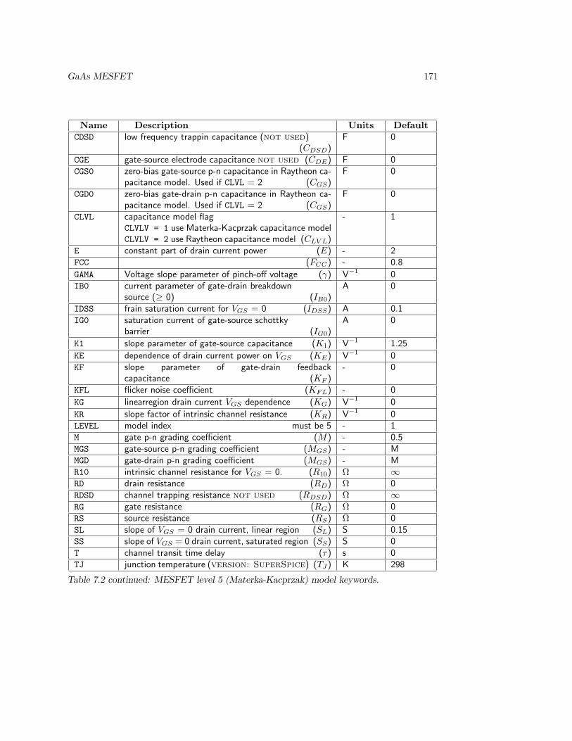
GaAs MESFET 171
Name Description Units DefaultCDSD low frequency trappin capacitance (not used)
(CDSD)F 0
CGE gate-source electrode capacitance not used (CDE) F 0CGS0 zero-bias gate-source p-n capacitance in Raytheon ca-
pacitance model. Used if CLVL = 2 (CGS)F 0
CGD0 zero-bias gate-drain p-n capacitance in Raytheon ca-pacitance model. Used if CLVL = 2 (CGS)
F 0
CLVL capacitance model flagCLVLV = 1 use Materka-Kacprzak capacitance modelCLVLV = 2 use Raytheon capacitance model (CLV L)
- 1
E constant part of drain current power (E) - 2FCC (FCC) - 0.8
GAMA Voltage slope parameter of pinch-off voltage (γ) V−1 0IB0 current parameter of gate-drain breakdown
source (≥ 0) (IB0)A 0
IDSS frain saturation current for VGS = 0 (IDSS) A 0.1IG0 saturation current of gate-source schottky
barrier (IG0)A 0
K1 slope parameter of gate-source capacitance (K1) V−1 1.25
KE dependence of drain current power on VGS (KE) V−1 0KF slope parameter of gate-drain feedback
capacitance (KF )- 0
KFL flicker noise coefficient (KFL) - 0
KG linearregion drain current VGS dependence (KG) V−1 0
KR slope factor of intrinsic channel resistance (KR) V−1 0LEVEL model index must be 5 - 1M gate p-n grading coefficient (M) - 0.5MGS gate-source p-n grading coefficient (MGS) - MMGD gate-drain p-n grading coefficient (MGS) - MR10 intrinsic channel resistance for VGS = 0. (R10) Ω ∞RD drain resistance (RD) Ω 0RDSD channel trapping resistance not used (RDSD) Ω ∞RG gate resistance (RG) Ω 0RS source resistance (RS) Ω 0SL slope of VGS = 0 drain current, linear region (SL) S 0.15SS slope of VGS = 0 drain current, saturated region (SS) S 0T channel transit time delay (τ) s 0TJ junction temperature (version: SuperSpice) (TJ) K 298
Table 7.2 continued: MESFET level 5 (Materka-Kacprzak) model keywords.
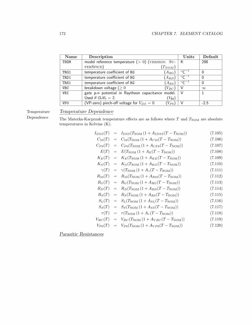
172 CHAPTER 7. ELEMENT CATALOG
Name Description Units DefaultTNOM model reference temperature (> 0) (version: Su-
perSpice) (TNOM )K 298
TRG1 temperature coefficient of RG (ARG) C−1 0
TRD1 temperature coefficient of RG (ARD) C−1 0
TRS1 temperature coefficient of RG (ARS) C−1 0VBC breakdown voltage (≥ 0 (VBC) V ∞VBI gate p-n potential in Raytheon capacitance model.
Used if CLVL = 2. (VBI)V 1
VP0 (VP-zero) pinch-off voltage for VDS = 0 (VP0) V -2.5
Temperature DependenceTemperatureDependence The Materka-Kacprzak temperature effects are as follows where T and TNOM are absolute
temperatures in Kelvins (K).
IDSS(T ) = IDSS(TNOM (1 + AIDSS(T − TNOM)) (7.105)C10(T ) = C10(TNOM (1 + AC10(T − TNOM)) (7.106)CF0(T ) = CF0(TNOM (1 + ACF0(T − TNOM)) (7.107)
E(T ) = E(TNOM (1 + AE(T − TNOM)) (7.108)KE(T ) = KE(TNOM (1 + AKE(T − TNOM)) (7.109)KG(T ) = KG(TNOM (1 + AKG(T − TNOM)) (7.110)
γ(T ) = γ(TNOM (1 + Aγ(T − TNOM)) (7.111)R10(T ) = R10(TNOM (1 + AR10(T − TNOM)) (7.112)RG(T ) = RG(TNOM (1 + ARG(T − TNOM)) (7.113)RD(T ) = RD(TNOM (1 + ARD(T − TNOM)) (7.114)RS(T ) = RS(TNOM (1 + ARS(T − TNOM)) (7.115)SL(T ) = SL(TNOM (1 + ASL(T − TNOM)) (7.116)SS(T ) = SS(TNOM (1 + ASS(T − TNOM)) (7.117)τ(T ) = τ(TNOM (1 + Aτ (T − TNOM)) (7.118)
VBC(T ) = VBC(TNOM (1 + AV BC(T − TNOM)) (7.119)VP0(T ) = VP0(TNOM (1 + AV P0(T − TNOM)) (7.120)
Parasitic Resistances
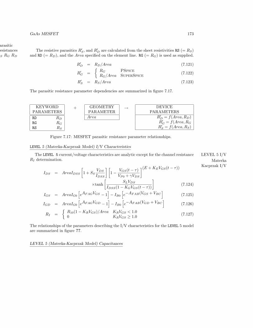
GaAs MESFET 173
ParasiticResistancesRS RG RD
The resistive parasitics R′S , and R′D are calculated from the sheet resistivities RS (= RS)and RD (= RD), and the Area specified on the element line. RG (= RG) is used as supplied.
R′D = RD/Area (7.121)
R′G =
RG PSpiceRG/Area SuperSpice
(7.122)
R′S = RS/Area (7.123)
The parasitic resistance parameter dependencies are summarized in figure 7.17.
KEYWORDPARAMETERSRD RD
RG RG
RS RS
+ GEOMETRYPARAMETERArea
→ DEVICEPARAMETERS
R′D = f(Area,RD)R′G = f(Area,RG
R′S = f(Area, RS)
Figure 7.17: MESFET parasitic resistance parameter relationships.
LEVEL 5 (Materka-Kacprzak Model) I/V Characteristics
The LEVEL 5 current/voltage characteristics are analytic except for the channel resistance LEVEL 5 I/VMaterka
Kacprzak I/VRI determination.
IDS = AreaIDSS
[1 + SS
VDS
IDSS
] [1− VGS(t− τ)
VP0 + γVDS
](E + KEVGS(t− τ))
×tanh[
SLVDS
IDSS(1−KGVGS(t− τ))
](7.124)
IGS = AreaIG0
[eAFAGVGS − 1
]− IB0
[e−AFAB(VGS + VBC
](7.125)
IGD = AreaIG0
[eAFAGVGD − 1
]− IB0
[e−AFAB(VGD + VBC
](7.126)
RI =
R10(1−KRVGS)/Area KRVGS < 1.00 KRVGS ≥ 1.0 (7.127)
The relationships of the parameters describing the I/V characteristics for the LEVEL 5 modelare summarized in figure ??.
LEVEL 5 (Materka-Kacprzak Model) Capacitances

174 CHAPTER 7. ELEMENT CATALOG
KEYWORDPARAMETERSAFAG AFAG
AFAB AFAB
GAMA γIDSS IDSS
IB0 IB0
IG0 IG0
KG KG
KE KE
KR KR
R10 R10
SS SS
SL SL
T τVBC VBC
VP0 VP0
+ GEOMETRYPARAMETER
Area
→ DEVICEPARAMETERS
IDS = f(Area, E, γ, IDSS ,KE , KG, SL, SS , τ, VP0)
IGS = f(Area, AFAB , AFAG,IB0, IG0, VBC)
IGD = f(Area,AFAB , AFAG,IB0, IG0, VBC)
RI = f(Area,KR, R10, VGS)
Figure 7.18: LEVEL 5 (Materka-Kacprzak model) I/V dependencies.
Two capacitance models are available depending on the value of the CLV L (CLVL) param- LEVEL 5Materka-Kacprzak
Capacitances
eter. With CLV L = 1 (default) the standard Materka capacitance model described below isused. With CLV L = 0 the Raytheon capacitance model described on page 159 is used. TheMaterka-Kacprzak capacitances are
C ′DS = Area CDS (7.128)
C ′GS =
Area[C10(1−K1VGS)MGS + C1S
]K1VGS < FCC
Area[C10(1− FCC)MGS + C1S
]K1VGS ≥ FCC
(7.129)
C ′GD =
Area[CF0(1−K1V1)MGD
]K1V1 < FCC
Area[CF0(1− FCC)MGD
]K1V1 ≥ FCC
(7.130)
The LEVEL 5 capacitance parameter dependencies are summarized in figure 7.19.
LEVEL 6 (Angelov Model)LEVEL 6Angelov The parameter keywords of the Materka-Kacprzak model are given in table 7.3.
Table 7.3 continued: MESFET LEVEL 6 (Angelov) model keywords.
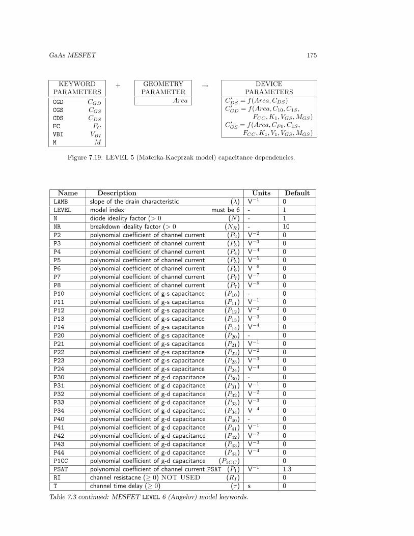
GaAs MESFET 175
KEYWORDPARAMETERSCGD CGD
CGS CGS
CDS CDS
FC FC
VBI VBI
M M
+ GEOMETRYPARAMETER
Area
→ DEVICEPARAMETERS
C ′DS = f(Area, CDS)C ′GD = f(Area,C10, C1S ,
FCC ,K1, VGS ,MGS)C ′GS = f(Area, CF0, C1S ,
FCC ,K1, V1, VGS ,MGS)
Figure 7.19: LEVEL 5 (Materka-Kacprzak model) capacitance dependencies.
Name Description Units DefaultLAMB slope of the drain characteristic (λ) V−1 0LEVEL model index must be 6 - 1N diode ideality factor (> 0 (N) - 1NR breakdown ideality factor (> 0 (NR) - 10P2 polynomial coefficient of channel current (P2) V−2 0P3 polynomial coefficient of channel current (P3) V−3 0P4 polynomial coefficient of channel current (P4) V−4 0P5 polynomial coefficient of channel current (P5) V−5 0P6 polynomial coefficient of channel current (P6) V−6 0P7 polynomial coefficient of channel current (P7) V−7 0P8 polynomial coefficient of channel current (P7) V−8 0P10 polynomial coefficient of g-s capacitance (P10) - 0P11 polynomial coefficient of g-s capacitance (P11) V−1 0P12 polynomial coefficient of g-s capacitance (P12) V−2 0P13 polynomial coefficient of g-s capacitance (P13) V−3 0P14 polynomial coefficient of g-s capacitance (P14) V−4 0P20 polynomial coefficient of g-s capacitance (P20) - 0P21 polynomial coefficient of g-s capacitance (P21) V−1 0P22 polynomial coefficient of g-s capacitance (P22) V−2 0P23 polynomial coefficient of g-s capacitance (P23) V−3 0P24 polynomial coefficient of g-s capacitance (P24) V−4 0P30 polynomial coefficient of g-d capacitance (P30) - 0P31 polynomial coefficient of g-d capacitance (P31) V−1 0P32 polynomial coefficient of g-d capacitance (P32) V−2 0P33 polynomial coefficient of g-d capacitance (P33) V−3 0P34 polynomial coefficient of g-d capacitance (P34) V−4 0P40 polynomial coefficient of g-d capacitance (P40) - 0P41 polynomial coefficient of g-d capacitance (P41) V−1 0P42 polynomial coefficient of g-d capacitance (P42) V−2 0P43 polynomial coefficient of g-d capacitance (P43) V−3 0P44 polynomial coefficient of g-d capacitance (P44) V−4 0P1CC polynomial coefficient of g-d capacitance (P1CC) 0PSAT polynomial coefficient of channel current PSAT (P1) V−1 1.3RI channel resistacne (≥ 0) NOT USED (RI) 0T channel time delay (≥ 0) (τ) s 0
Table 7.3 continued: MESFET LEVEL 6 (Angelov) model keywords.

176 CHAPTER 7. ELEMENT CATALOG
Name Description Units DefaultTJ junction temperature (TJ) K 298TM IDS linear temperature coefficient (TM ) 0TME IDS power law temperature coefficient (TME) 0TNOM model reference temperature (> 0) (TNOM ) K 298VBD breakdown voltage (VBD) 0VPK0 gate-source voltage for unsaturated peak gm (VPK0) V -0.5VPKS gate-source voltage for peak gm (VPKS) V 0XTI saturation current temperature exponent (XTI) 2
Temperature DependenceTemperatureDependence Temperature effects are incorporated as follows where T and TNOM are absolute tempera-
tures in Kelvins (K) and the thermal voltage VTH = kT/q.
α(T ) = α(TNOM) (1 + Aα(T − TNOM)) (7.131)CGS0(T ) = CGS0(TNOM)
(1 + ACGS(T − TNOM) + BCGS(T − TNOM)2
)(7.132)
CGD0(T ) = CGD0(TNOM)(1 + ACGD(T − TNOM) + BCGD(T − TNOM)2
)(7.133)
EG(T ) = EG(0)− FGAP14T 2/ (T + FGAP2) (7.134)γ(T ) = γ(TNOM) (1 + Aγ(T − TNOM)) (7.135)
IPK(T ) = IPK(TNOM) (1 + AIPK(T − TNOM)) (7.136)RI(T ) = RI(TNOM)
(1 + ARI(T − TNOM) + BRI(T − TNOM)2
)(7.137)
RG(T ) = RG(TNOM)(1 + ARG(T − TNOM) + BRG(T − TNOM)2
)(7.138)
RD(T ) = RD(TNOM)(1 + ARD(T − TNOM) + BRD(T − TNOM)2
)(7.139)
RS(T ) = RS(TNOM)(1 + ARS(T − TNOM) + BRS(T − TNOM)2
)(7.140)
VPK(T ) = VPK(TNOM) (1 + AV PK(T − TNOM)) (7.141)VBD(T ) = VBD(TNOM) (1 + AV BD(T − TNOM)) (7.142)
TMIDSTME???? (7.143)
Parasitic Resistances
The resistive parasitics R′S , and R′D are calculated from the sheet resistivities RS (= RS)ParasiticResistancesRS RG RD
and RD (= RD), and the Area specified on the element line. RG (= RG) is used as supplied.
R′D = RD/Area (7.144)R′G = RG/Area (7.145)R′S = RS/Area (7.146)
The parasitic resistance parameter dependencies are summarized in figure 7.20.LEVEL 6 (Angelov Model) I/V Characteristics
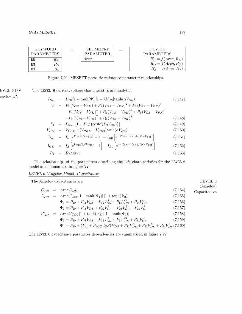
GaAs MESFET 177
KEYWORDPARAMETERSRD RD
RG RG
RS RS
+ GEOMETRYPARAMETERArea
→ DEVICEPARAMETERS
R′D = f(Area,RD)R′G = f(Area, RG)R′S = f(Area, RS)
Figure 7.20: MESFET parasitic resistance parameter relationships.
The LEVEL 6 current/voltage characteristics are analytic:LEVEL 6 I/VAngelov I/V
IDS = IPK [1 + tanh(Ψ)][1 + λVDS ]tanh(αVDS) (7.147)
Ψ = P1 (VGS − VPK) + P2 (VGS − VPK)2 + P3 (VGS − VPK)3
+P4 (VGS − VPK)4 + P5 (VGS − VPK)5 + P6 (VGS − VPK)6
+P7 (VGS − VPK)7 + P8 (VGS − VPK)8 (7.148)P1 = PSAT
[1 + B1/
(cosh2(B2VDS)
)](7.149)
VPK = VPK0 + (VPKS − VPK0)tanh(αVDS) (7.150)
IGS = IS
[eVGS/(NVTH) − 1
]− IB0
[e−(VGS+VBD)/(NRVTH)
](7.151)
IGD = IS
[eVGD/(NVTH) − 1
]− IB0
[e−(VGD+VBD)/(NRVTH)
](7.152)
RI = R′I/Area (7.153)
The relationships of the parameters describing the I/V characteristics for the LEVEL 6model are summarized in figure ??.
LEVEL 6 (Angelov Model) Capacitances
The Angelov capacitances are LEVEL 6(Angelov)
CapacitancesC ′DS = AreaCDS (7.154)C ′GS = AreaCGS0 [1 + tanh(Ψ1)] [1 + tanh(Ψ2)] (7.155)
Ψ1 = P10 + P11VGS + P12V2GS + P13V
3GS + P14V
4GS (7.156)
Ψ2 = P20 + P11VDS + P22V2DS + P23V
3DS + P24V
4DS (7.157)
C ′GD = AreaCGD0 [1 + tanh(Ψ3)] [1− tanh(Ψ4)] (7.158)Ψ3 = P30 + P31VGS + P32V
2GS + P33V
3GS + P34V
4GS (7.159)
Ψ4 = P40 + (P41 + P1CCVGS)VDS + P42V2DS + P43V
3DS + P44V
4DS (7.160)
The LEVEL 6 capacitance parameter dependencies are summarized in figure 7.22.
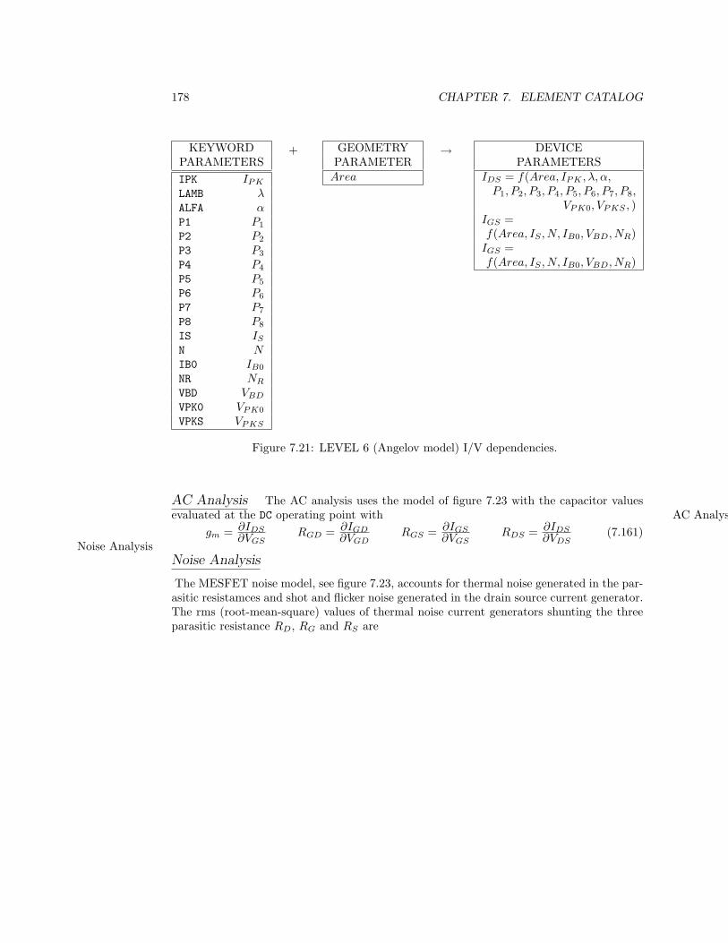
178 CHAPTER 7. ELEMENT CATALOG
KEYWORDPARAMETERSIPK IPK
LAMB λALFA αP1 P1
P2 P2
P3 P3
P4 P4
P5 P5
P6 P6
P7 P7
P8 P8
IS IS
N NIB0 IB0
NR NR
VBD VBD
VPK0 VPK0
VPKS VPKS
+ GEOMETRYPARAMETERArea
→ DEVICEPARAMETERS
IDS = f(Area, IPK , λ, α,P1, P2, P3, P4, P5, P6, P7, P8,
VPK0, VPKS , )IGS =f(Area, IS , N, IB0, VBD, NR)
IGS =f(Area, IS , N, IB0, VBD, NR)
Figure 7.21: LEVEL 6 (Angelov model) I/V dependencies.
AC Analysis The AC analysis uses the model of figure 7.23 with the capacitor valuesAC Analysisevaluated at the DC operating point with
gm = ∂IDS∂VGS
RGD = ∂IGD∂VGD
RGS = ∂IGS∂VGS
RDS = ∂IDS∂VDS
(7.161)Noise Analysis
Noise Analysis
The MESFET noise model, see figure 7.23, accounts for thermal noise generated in the par-asitic resistamces and shot and flicker noise generated in the drain source current generator.The rms (root-mean-square) values of thermal noise current generators shunting the threeparasitic resistance RD, RG and RS are
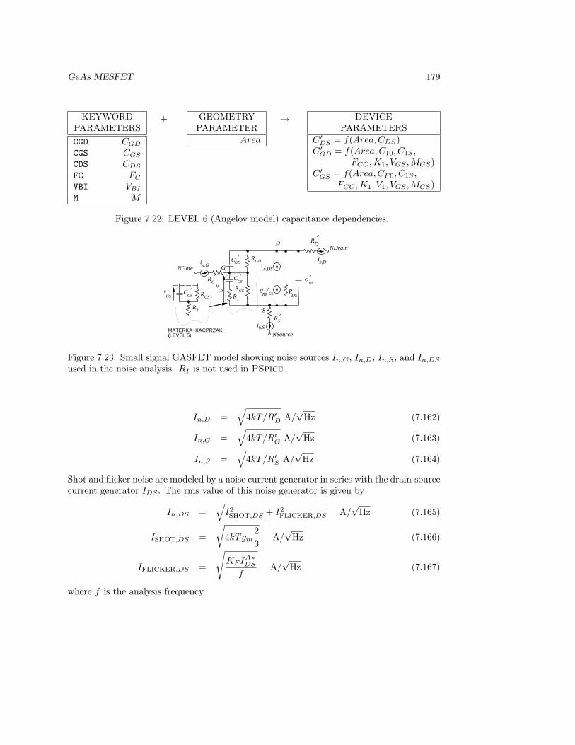
GaAs MESFET 179
KEYWORDPARAMETERSCGD CGD
CGS CGS
CDS CDS
FC FC
VBI VBI
M M
+ GEOMETRYPARAMETER
Area
→ DEVICEPARAMETERS
C ′DS = f(Area, CDS)C ′GD = f(Area,C10, C1S ,
FCC ,K1, VGS ,MGS)C ′GS = f(Area, CF0, C1S ,
FCC ,K1, V1, VGS ,MGS)
Figure 7.22: LEVEL 6 (Angelov model) capacitance dependencies.
NGate G
S
NSource
NDrainD
RG
CGS
RI
RS
RD
CGD
CDS
CGS
RI
MATERKA−KACPRZAK(LEVEL 5)
GSv GS
vgm R
DS
in,DS
n,Si
n,Gi n,D
iRGD
RGS
RGS
GSv
Figure 7.23: Small signal GASFET model showing noise sources In,G, In,D, In,S , and In,DS
used in the noise analysis. RI is not used in PSpice.
In,D =√
4kT/R′D A/√
Hz (7.162)
In,G =√
4kT/R′G A/√
Hz (7.163)
In,S =√
4kT/R′S A/√
Hz (7.164)
Shot and flicker noise are modeled by a noise current generator in series with the drain-sourcecurrent generator IDS . The rms value of this noise generator is given by
In,DS =√
I2SHOT,DS + I2
FLICKER,DS A/√
Hz (7.165)
ISHOT,DS =
√4kTgm
23
A/√
Hz (7.166)
IFLICKER,DS =
√KF IAF
DS
fA/√
Hz (7.167)
where f is the analysis frequency.
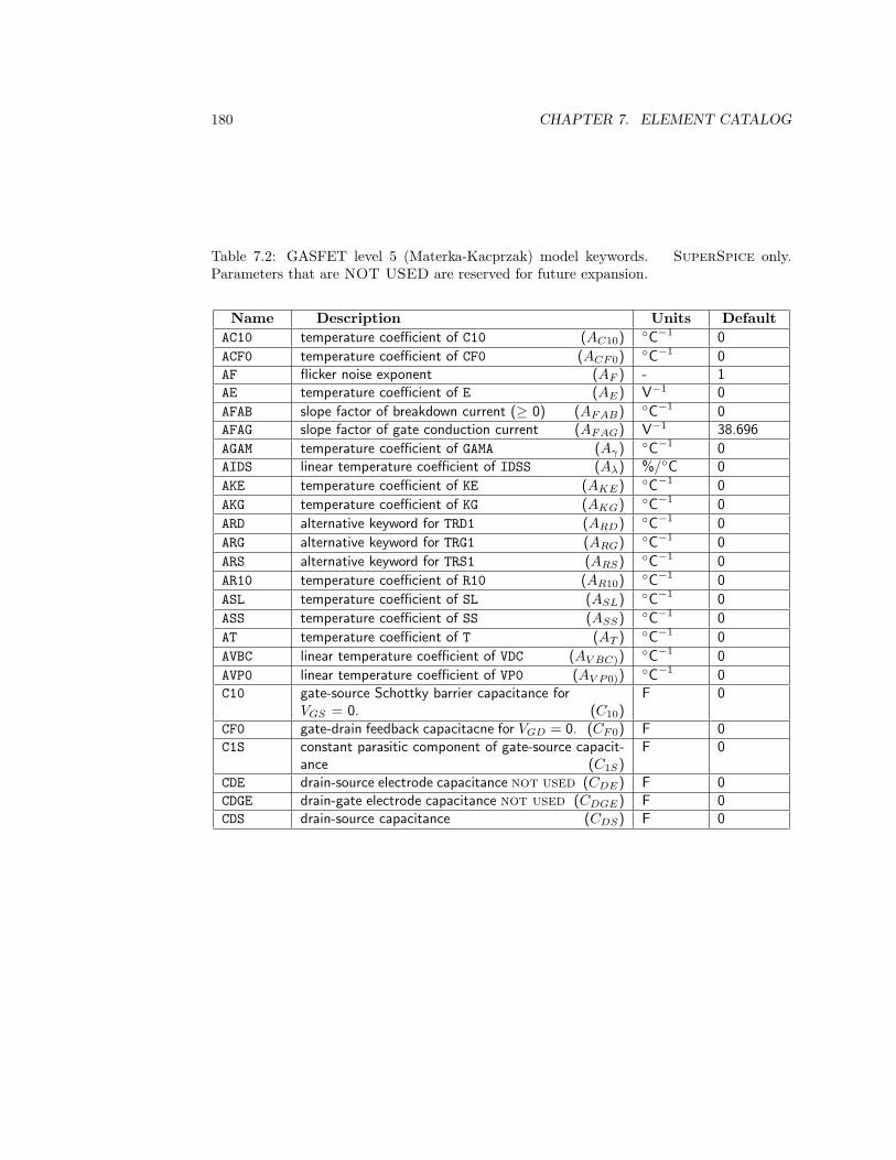
180 CHAPTER 7. ELEMENT CATALOG
Table 7.2: GASFET level 5 (Materka-Kacprzak) model keywords. SuperSpice only.Parameters that are NOT USED are reserved for future expansion.
Name Description Units DefaultAC10 temperature coefficient of C10 (AC10)
C−1 0
ACF0 temperature coefficient of CF0 (ACF0)C−1 0
AF flicker noise exponent (AF ) - 1AE temperature coefficient of E (AE) V−1 0
AFAB slope factor of breakdown current (≥ 0) (AFAB) C−1 0AFAG slope factor of gate conduction current (AFAG) V−1 38.696
AGAM temperature coefficient of GAMA (Aγ) C−1 0AIDS linear temperature coefficient of IDSS (Aλ) %/C 0
AKE temperature coefficient of KE (AKE) C−1 0
AKG temperature coefficient of KG (AKG) C−1 0
ARD alternative keyword for TRD1 (ARD) C−1 0
ARG alternative keyword for TRG1 (ARG) C−1 0
ARS alternative keyword for TRS1 (ARS) C−1 0
AR10 temperature coefficient of R10 (AR10)C−1 0
ASL temperature coefficient of SL (ASL) C−1 0
ASS temperature coefficient of SS (ASS) C−1 0
AT temperature coefficient of T (AT ) C−1 0
AVBC linear temperature coefficient of VDC (AV BC))C−1 0
AVP0 linear temperature coefficient of VP0 (AV P0))C−1 0
C10 gate-source Schottky barrier capacitance forVGS = 0. (C10)
F 0
CF0 gate-drain feedback capacitacne for VGD = 0. (CF0) F 0C1S constant parasitic component of gate-source capacit-
ance (C1S)F 0
CDE drain-source electrode capacitance not used (CDE) F 0CDGE drain-gate electrode capacitance not used (CDGE) F 0CDS drain-source capacitance (CDS) F 0
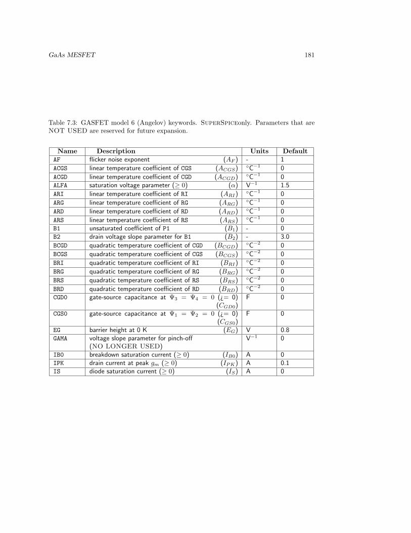
GaAs MESFET 181
Table 7.3: GASFET model 6 (Angelov) keywords. SuperSpiceonly. Parameters that areNOT USED are reserved for future expansion.
Name Description Units DefaultAF flicker noise exponent (AF ) - 1
ACGS linear temperature coefficient of CGS (ACGS) C−1 0
ACGD linear temperature coefficient of CGD (ACGD) C−1 0ALFA saturation voltage parameter (≥ 0) (α) V−1 1.5
ARI linear temperature coefficient of RI (ARI)C−1 0
ARG linear temperature coefficient of RG (ARG) C−1 0
ARD linear temperature coefficient of RD (ARD) C−1 0
ARS linear temperature coefficient of RS (ARS) C−1 0B1 unsaturated coefficient of P1 (B1) - 0B2 drain voltage slope parameter for B1 (B2) - 3.0
BCGD quadratic temperature coefficient of CGD (BCGD) C−2 0
BCGS quadratic temperature coefficient of CGS (BCGS) C−2 0
BRI quadratic temperature coefficient of RI (BRI)C−2 0
BRG quadratic temperature coefficient of RG (BRG) C−2 0
BRS quadratic temperature coefficient of RS (BRS) C−2 0
BRD quadratic temperature coefficient of RD (BRD) C−2 0CGD0 gate-source capacitance at Ψ3 = Ψ4 = 0 (¿= 0)
(CGD0)F 0
CGS0 gate-source capacitance at Ψ1 = Ψ2 = 0 (¿= 0)(CGS0)
F 0
EG barrier height at 0 K (EG) V 0.8GAMA voltage slope parameter for pinch-off
(NO LONGER USED)V−1 0
IB0 breakdown saturation current (≥ 0) (IB0) A 0IPK drain current at peak gm (≥ 0) (IPK) A 0.1IS diode saturation current (≥ 0) (IS) A 0
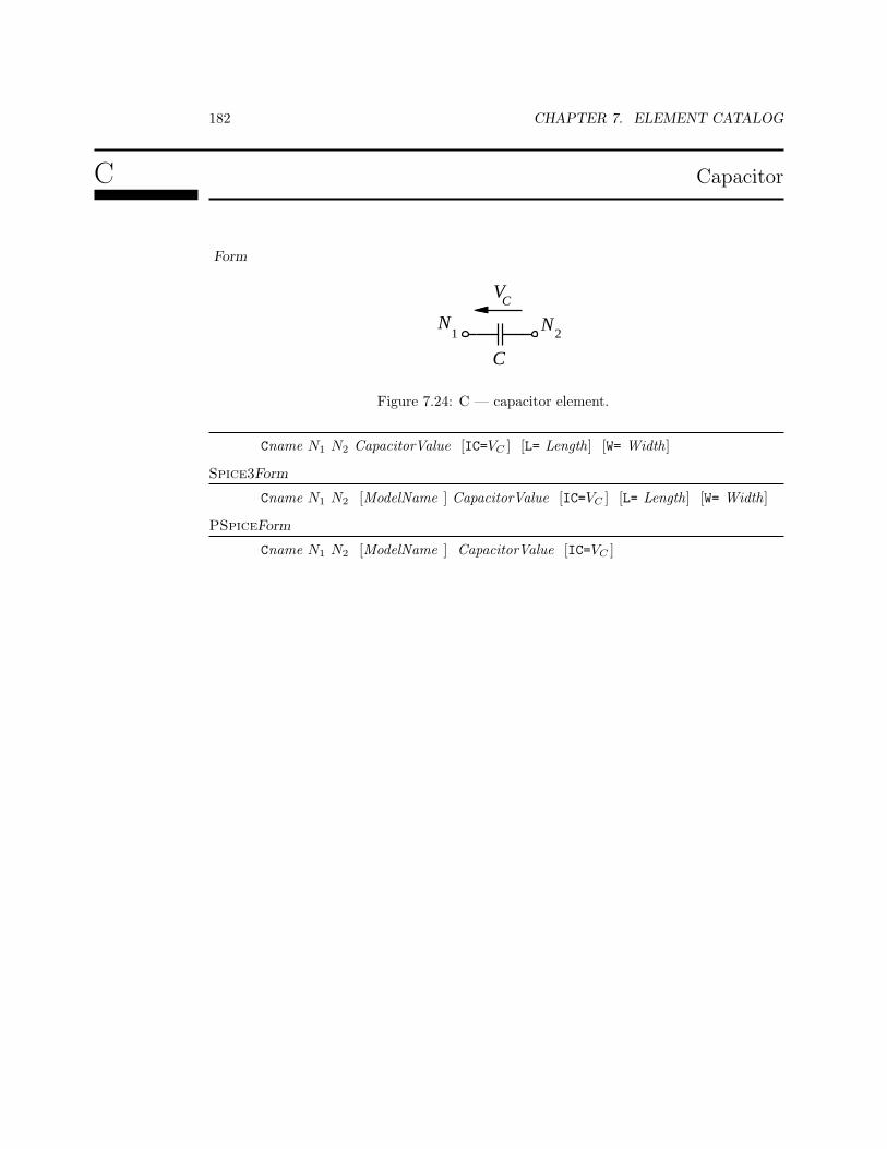
182 CHAPTER 7. ELEMENT CATALOG
C Capacitor
Form
1 2
C
VC
N N
Figure 7.24: C — capacitor element.
Cname N1 N2 CapacitorValue [IC=VC ] [L= Length] [W= Width]
Spice3Form
Cname N1 N2 [ModelName ] CapacitorValue [IC=VC ] [L= Length] [W= Width]
PSpiceForm
Cname N1 N2 [ModelName ] CapacitorValue [IC=VC ]
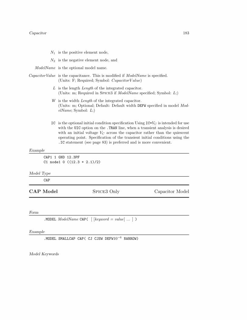
Capacitor 183
N1 is the positive element node,
N2 is the negative element node, and
ModelName is the optional model name.
CapacitorValue is the capacitance. This is modified if ModelName is specified.(Units: F; Required; Symbol: CapacitorV alue)
L is the length Length of the integrated capacitor.(Units: m; Required in Spice3 if ModelName specified; Symbol: L;)
W is the width Length of the integrated capacitor.(Units: m; Optional; Default: Default width DEFW specified in model Mod-elName; Symbol: L;)
IC is the optional initial condition specification Using IC=VC is intended for usewith the UIC option on the .TRAN line, when a transient analysis is desiredwith an initial voltage VC across the capacitor rather than the quiescentoperating point. Specification of the transient initial conditions using the.IC statement (see page 83) is preferred and is more convenient.
Example
CAP1 1 GND 12.3PFC1 node1 0 ((12.3 + 2.1)/2)
Model Type
CAP
CAP Model Spice3 Only Capacitor Model
Form
.MODEL ModelName CAP( [ [keyword = value] ... ] )
Example
.MODEL SMALLCAP CAP( CJ CJSW DEFW10−6 NARROW)
Model Keywords
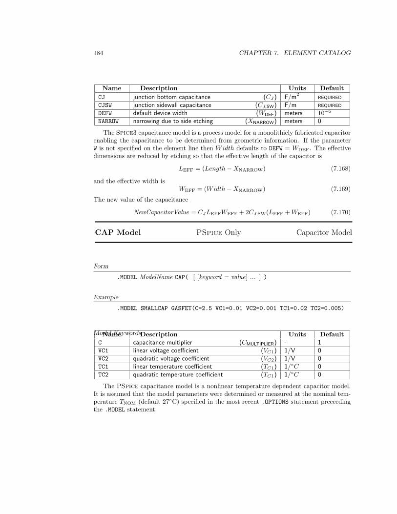
184 CHAPTER 7. ELEMENT CATALOG
Name Description Units DefaultCJ junction bottom capacitance (CJ) F/m2
REQUIRED
CJSW junction sidewall capacitance (CJ,SW) F/m REQUIRED
DEFW default device width (WDEF) meters 10−6
NARROW narrowing due to side etching (XNARROW) meters 0
The Spice3 capacitance model is a process model for a monolithicly fabricated capacitorenabling the capacitance to be determined from geometric information. If the parameterW is not specified on the element line then Width defaults to DEFW = WDEF. The effectivedimensions are reduced by etching so that the effective length of the capacitor is
LEFF = (Length−XNARROW) (7.168)
and the effective width isWEFF = (Width−XNARROW) (7.169)
The new value of the capacitance
NewCapacitorValue = CJLEFFWEFF + 2CJ,SW(LEFF + WEFF) (7.170)
CAP Model PSpice Only Capacitor Model
Form
.MODEL ModelName CAP( [ [keyword = value] ... ] )
Example
.MODEL SMALLCAP GASFET(C=2.5 VC1=0.01 VC2=0.001 TC1=0.02 TC2=0.005)
Model KeywordsName Description Units DefaultC capacitance multiplier (CMULTIPLIER) - 1VC1 linear voltage coefficient (VC1) 1/V 0VC2 quadratic voltage coefficient (VC2) 1/V 0TC1 linear temperature coefficient (TC1) 1/C 0TC2 quadratic temperature coefficient (TC1) 1/C 0
The PSpice capacitance model is a nonlinear temperature dependent capacitor model.It is assumed that the model parameters were determined or measured at the nominal tem-perature TNOM (default 27C) specified in the most recent .OPTIONS statement preceedingthe .MODEL statement.
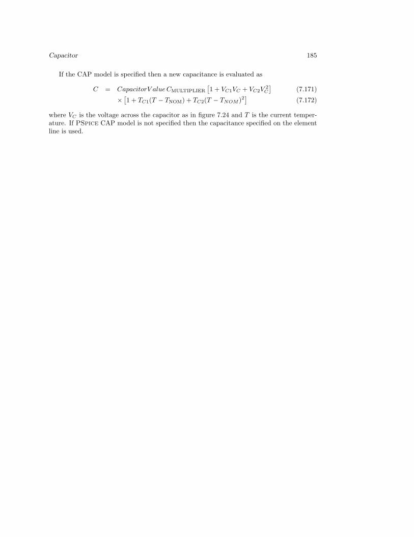
Capacitor 185
If the CAP model is specified then a new capacitance is evaluated as
C = CapacitorV alue CMULTIPLIER
[1 + VC1VC + VC2V
2C
](7.171)
× [1 + TC1(T − TNOM) + TC2(T − TNOM )2
](7.172)
where VC is the voltage across the capacitor as in figure 7.24 and T is the current temper-ature. If PSpice CAP model is not specified then the capacitance specified on the elementline is used.

186 CHAPTER 7. ELEMENT CATALOG
D Diode
NCathodeNAnode
Figure 7.25: D — diode element.
Form
Dname n1 n2 ModelName [Area] [OFF] [IC=VD ]
PSpiceForm
Dname n1 n2 ModelName [Area] [OFF]
n1 is the positive (anode) diode node.
n1 is the negative (cathode) diode node.
ModelName is the model name.
Area is an optional relative area factor.(Units: none; Optional; Default: 1, Symbol: Area)
OFF indicates an (optional) starting condition on the device for DC operatingpoint analysis. If specified the DC operating point is calculated with theterminal voltages set to zero. Once convergence is obtained, the programcontinues to iterate to obtain the exact value of the terminal voltages. TheOFF option is used to enforce the solution to correspond to a desired stateif the circuit has more than one stable state.
IC is the (optional) initial condition specification. Using IC = VD is intendedfor use with the UIC option on the other than the quiescent operating point.Specification of the transient initial conditions using the .IC statement (seepage 83) is preferred and is more convenient.
Example
DBRIDGE 2 10 DIODE1DCLMP 3 7 DMOD 3.0 IC=0.2
Model Type

Diode 187
DIODE
DIODE Model Diode Model
VD C ID
RS
NCathode
NAnode
Figure 7.26: Schematic of diode element model.
Note
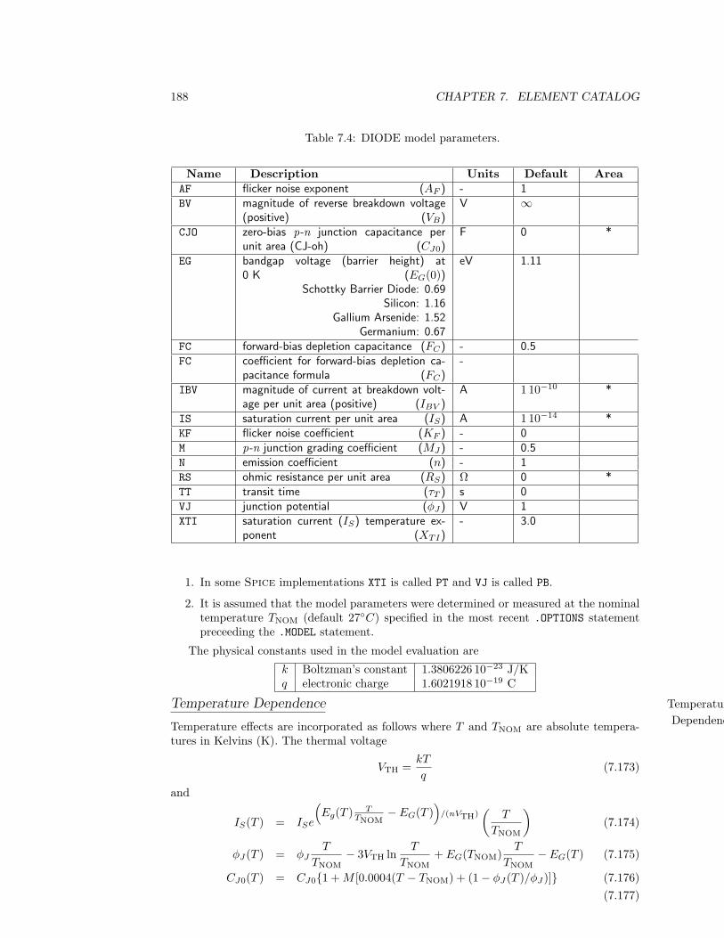
188 CHAPTER 7. ELEMENT CATALOG
Table 7.4: DIODE model parameters.
Name Description Units Default AreaAF flicker noise exponent (AF ) - 1BV magnitude of reverse breakdown voltage
(positive) (VB)V ∞
CJO zero-bias p-n junction capacitance perunit area (CJ-oh) (CJ0)
F 0 *
EG bandgap voltage (barrier height) at0 K (EG(0))
Schottky Barrier Diode: 0.69Silicon: 1.16
Gallium Arsenide: 1.52Germanium: 0.67
eV 1.11
FC forward-bias depletion capacitance (FC) - 0.5FC coefficient for forward-bias depletion ca-
pacitance formula (FC)-
IBV magnitude of current at breakdown volt-age per unit area (positive) (IBV )
A 1 10−10 *
IS saturation current per unit area (IS) A 1 10−14 *KF flicker noise coefficient (KF ) - 0M p-n junction grading coefficient (MJ) - 0.5N emission coefficient (n) - 1RS ohmic resistance per unit area (RS) Ω 0 *TT transit time (τT ) s 0VJ junction potential (φJ) V 1XTI saturation current (IS) temperature ex-
ponent (XTI)- 3.0
1. In some Spice implementations XTI is called PT and VJ is called PB.
2. It is assumed that the model parameters were determined or measured at the nominaltemperature TNOM (default 27C) specified in the most recent .OPTIONS statementpreceeding the .MODEL statement.
The physical constants used in the model evaluation are
k Boltzman’s constant 1.3806226 10−23 J/Kq electronic charge 1.6021918 10−19 C
Temperature Dependence TemperatureDependenceTemperature effects are incorporated as follows where T and TNOM are absolute tempera-
tures in Kelvins (K). The thermal voltage
VTH =kT
q(7.173)
and
IS(T ) = ISe
(Eg(T ) T
TNOM− EG(T )
)/(nVTH)
(T
TNOM
)(7.174)
φJ(T ) = φJT
TNOM− 3VTH ln
T
TNOM+ EG(TNOM)
T
TNOM− EG(T ) (7.175)
CJ0(T ) = CJ01 + M [0.0004(T − TNOM) + (1− φJ (T )/φJ)] (7.176)(7.177)
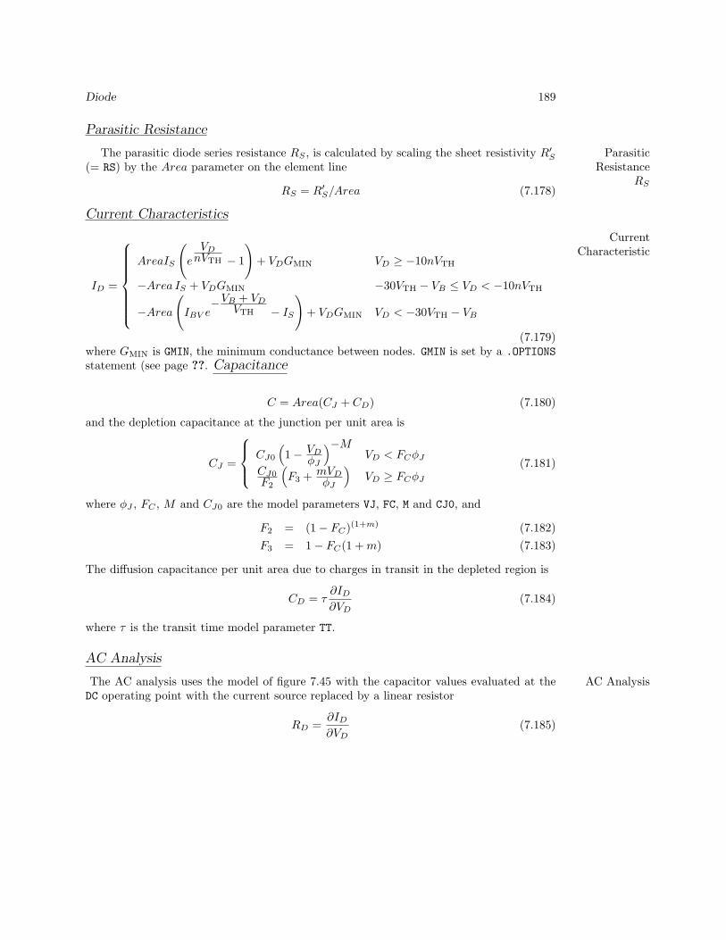
Diode 189
Parasitic Resistance
The parasitic diode series resistance RS , is calculated by scaling the sheet resistivity R′S ParasiticResistance
RS
(= RS) by the Area parameter on the element line
RS = R′S/Area (7.178)
Current Characteristics
CurrentCharacteristic
ID =
AreaIS
(e
VDnVTH − 1
)+ VDGMIN VD ≥ −10nVTH
−Area IS + VDGMIN −30VTH − VB ≤ VD < −10nVTH
−Area
(IBV e
−VB + VDVTH − IS
)+ VDGMIN VD < −30VTH − VB
(7.179)where GMIN is GMIN, the minimum conductance between nodes. GMIN is set by a .OPTIONSstatement (see page ??. Capacitance
C = Area(CJ + CD) (7.180)
and the depletion capacitance at the junction per unit area is
CJ =
CJ0
(1− VD
φJ
)−MVD < FCφJ
CJ0F2
(F3 + mVD
φJ
)VD ≥ FCφJ
(7.181)
where φJ , FC , M and CJ0 are the model parameters VJ, FC, M and CJ0, and
F2 = (1− FC)(1+m) (7.182)F3 = 1− FC(1 + m) (7.183)
The diffusion capacitance per unit area due to charges in transit in the depleted region is
CD = τ∂ID
∂VD(7.184)
where τ is the transit time model parameter TT.
AC Analysis
The AC analysis uses the model of figure 7.45 with the capacitor values evaluated at the AC AnalysisDC operating point with the current source replaced by a linear resistor
RD =∂ID
∂VD(7.185)
190 CHAPTER 7. ELEMENT CATALOG
Noise Analysis
The DIODE noise model accounts for thermal noise generated in the parasitic seriesNoise Analysis resistance and shot and flicker noise generated in the the junction. The rms (root-mean-
square) value of the thermal noise current generators shunting RS isNoise Model
In,S =√
4kT/RS A/√
Hz (7.186)
The RMS value of noise current generators shunting RD in the AC model is
In,J =(I2SHOT + I2
FLICKER
)(7.187)
where the RMS shot noise current is
ISHOT =√
2qID A/√
Hz A/√
Hz (7.188)
and the RMS flicker noise current is
IFLICKER =
√KF IAF
D
fKCHANNELA/√
Hz (7.189)
where f is the analysis frequency and RD is the ACjunction resistance in (7.185)
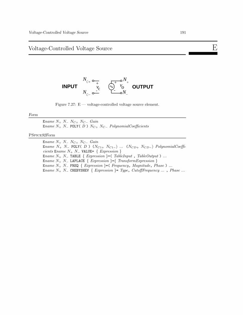
Voltage-Controlled Voltage Source 191
Voltage-Controlled Voltage Source E
+
-
C+
C-
v+
- c
+
-vo OUTPUT
N N
NNINPUT
Figure 7.27: E — voltage-controlled voltage source element.
Form
Ename N+ N− NC+ NC− GainEname N+ N− POLY( D ) NC+ NC− PolynomialCoefficients
PSpice92Form
Ename N+ N− NC+ NC− GainEname N+ N− POLY( D ) (NC1+ NC1−) ... (NCD+ NCD−) PolynomialCoeffi-cients Ename N+ N− VALUE= Expression Ename N+ N− TABLE Expression =( TableInput , TableOutput ) ...Ename N+ N− LAPLACE Expression = TransformExpression Ename N+ N− FREQ Expression =( Frequency, Magnitude, Phase ) ...Ename N+ N− CHEBYSHEV Expression = Type, CutoffFrequency ... , Phase ...
192 CHAPTER 7. ELEMENT CATALOG
N+ is the positive voltage source node.
N− is the negative voltage source node.
NC+ is the positive controlling node.
NC− is the negative controlling node.
Gain is the voltage gain.
POLY is the identifier for the polynomial form of the element
D is the degree of the poynomial. The number of pairs of controlling nodesmust be equal to Degree.
NCi+ the positive node of the i th controlling node pair.
NCi− the negative node of the i th controlling node pair.
PolynomialCoefficients is the set of polynomial coefficients which must be specified in thestandard polynomial coefficient format discussed on page 59.
VALUE is the identifier for the value form of the element.
Expression This is an expression of the form discussed on page 59.
TABLE is the identifier for the table form of the element.
TableInput This is the independent input of the table. See the TABLE parameter above.
TableInput This is the dependent output of the table. See the TABLE parameter above.
LAPLACE is the identifier for the laplace form of the element.
TransformExpression
FREQ is the identifier for the frequency form of the element.
Frequency
Magnitude
Phase
CHEBYSHEV is the identifier for the chebyshev form of the element.
Type
CutoffFrequency
Phase
Example

Voltage-Controlled Voltage Source 193
E1 2 3 14 1 2.0Note
1. Several form of the voltage-controlled voltage source element are supported in additionto the Linear Gain form which is the default. The other forms are selected based onthe the identifier POLY, VALUE, TABLE, LAPLACE, FREQ or CHEBYSHEV.
Linear Gain Instance
Ename N+ N− NC+ NC− Gain
The value of the voltage generator is linearly proportional to the controlling voltage:
vo = Gain vc (7.190)
POLYnomial Instance
Ename N+ N− POLY( D ) (NC1+ NC1−) ... (NCD+ NCD−) PolynomialCoefficients
The value of the voltage generator is a polynomial function of the controlling voltages:
vo = f(vc1, ..., vci, ...vcD) (7.191)
where the number of controlling voltages is D — the degree of the polynomial specified onthe element line. vci is the ith controlling voltage and is the voltage of the nci+ node withrespect to the nci+ node.
VALUE Instance — PSpice92 only
Ename N+ N− VALUE= Expression The value of the voltage generator is the resultant of an expression evaluation.
vo = f(vc) (7.192)
TABLE Instance — PSpice92 only
Ename N+ N− TABLE Expression =( TableInput , TableOutput ) ...
vo = f(vc) (7.193)

194 CHAPTER 7. ELEMENT CATALOG
LAPLACE Instance — PSpice92 only
Ename N+ N− LAPLACE Expression = TransformExpression
vo = f(vc) (7.194)
FREQ — PSpice92 only
Ename N+ N− FREQ Expression =( Frequency, Magnitude, Phase ) ...
vo = f(vc) (7.195)
CHEBYSHEV — PSpice92 only
Ename N+ N− CHEBYSHEV Expression = Type, CutoffFrequency ... , Phase ...
Current-Controlled Current Source 195
Current-Controlled Current Source F
+
-
ic
VoltageSourceName
+
-
iO
INPUT OUTPUTN
NN
NC
C
+
-
Figure 7.28: F — current-controlled current source element.
Form
Fname N+ N− VoltageSourceName GainFname N+ N− POLY( D ) VoltageSourceName1 ... VoltageSourceNameD Polyno-mialCoefficients
N+ is the positive voltage source node.
N− is the negative voltage source node.
VoltageSourceName is the name of the voltage source the current through which is thecontrolling current. The voltage source must be a V element.
Gain is the current gain.
POLY is the identifier for the polynomial form of the element
D is the degree of the poynomial. The number of pairs of controlling nodesmust be equal to Degree.
VoltageSourceNamei is the name of the voltage source the current through which is the ithcontrolling current. The voltage source must be a V element.
PolynomialCoefficients is the set of polynomial coefficients which must be specified in thestandard polynomial coefficient format discussed on page 59.
Example
E1 2 3 14 1 2.0Linear Gain Instance
196 CHAPTER 7. ELEMENT CATALOG
Fname N+ N− NC+ NC− Gain
The value of the voltage generator is linearly proportional to the controlling current:
vo = Gain vc (7.196)
POLYnomial Instance
Fname N+ N− POLY( D ) (NC1+ NC1−) ... (NCD+ NCD−) PolynomialCoefficients
The value of the voltage generator is a polynomial function of the controlling voltages:
vo = f(ic1, ..., ici, ...icD) (7.197)
where the number of controlling currents is D — the degree of the polynomial specified onthe element line. ici is the ith controlling current and is the current flowing from the +terminal to the − terminal in the ith voltage source of name VoltageSourceName.

Voltage-Controlled Current Source 197
Voltage-Controlled Current Source G
+
-
C+
C-
v+
-
iON
N N
NINPUT OUTPUT
Figure 7.29: G — voltage-controlled current source element.
Form
Gname N+ N− NC+ NC− TransconductanceGname N+ N− POLY( D ) NC+ NC− PolynomialCoefficients
PSpice92Form
Gname N+ N− NC+ NC− TransconductanceGname N+ N− POLY( D ) (NC1+ NC1−) ... (NCD+ NCD−) PolynomialCoeffi-cients Gname N+ N− VALUE= Expression Gname N+ N− TABLE Expression =( TableInput , TableOutput ) ...Gname N+ N− LAPLACE Expression = TransformExpression Gname N+ N− FREQ Expression =( Frequency, Magnitude, Phase ) ...Gname N+ N− CHEBYSHEV Expression = Type, CutoffFrequency ... , Phase ...

198 CHAPTER 7. ELEMENT CATALOG
N+ is the positive voltage source node.
N− is the negative voltage source node.
NC+ is the positive controlling node.
NC− is the negative controlling node.
Transconductance is the transconductance.
POLY is the identifier for the polynomial form of the element
D is the degree of the poynomial. The number of pairs of controlling nodesmust be equal to Degree.
NCi+ the positive node of the i th controlling node pair.
NCi− the negative node of the i th controlling node pair.
PolynomialCoefficients is the set of polynomial coefficients which must be specified in thestandard polynomial coefficient format discussed on page 59.
VALUE is the identifier for the value form of the element.
Expression This is an expression of the form discussed on page 59.
TABLE is the identifier for the table form of the element.
TableInput This is the independent input of the table. See the TABLE parameter above.
TableInput This is the dependent output of the table. See the TABLE parameter above.
LAPLACE is the identifier for the laplace form of the element.
TransformExpression
FREQ is the identifier for the frequency form of the element.
Frequency
Magnitude
Phase
CHEBYSHEV is the identifier for the chebyshev form of the element.
Type
CutoffFrequency
Phase
Example
Voltage-Controlled Current Source 199
G1 2 3 14 1 2.0
Note
1. Several form of the voltage-controlled voltage source element are supported in additionto the Linear Transconductance form which is the default. The other forms are selectedbased on the the identifier POLY, VALUE, TABLE, LAPLACE, FREQ or CHEBYSHEV.
Linear Transconductance Instance
Gname N+ N− NC+ NC− Transconductance
The value of the voltage generator is linearly proportional to the controlling voltage:
vo = Transconductance vc (7.198)
POLYnomial Instance
Gname N+ N− POLY( D ) (NC1+ NC1−) ... (NCD+ NCD−) PolynomialCoefficients
The value of the voltage generator is a polynomial function of the controlling voltages:
vo = f(vc1, ..., vci, ...vcD) (7.199)
where the number of controlling voltages is D — the degree of the polynomial specified onthe element line. vci is the ith controlling voltage and is the voltage of the nci+ node withrespect to the nci+ node.
VALUE Instance — PSpice92 only
Gname N+ N− VALUE= Expression The value of the voltage generator is the resultant of an expression evaluation.
vo = f(vc) (7.200)
TABLE Instance — PSpice92 only
Gname N+ N− TABLE Expression =( TableInput , TableOutput ) ...
vo = f(vc) (7.201)
200 CHAPTER 7. ELEMENT CATALOG
LAPLACE Instance — PSpice92 only
Gname N+ N− LAPLACE Expression = TransformExpression
vo = f(vc) (7.202)
FREQ — PSpice92 only
Gname N+ N− FREQ Expression =( Frequency, Magnitude, Phase ) ...
vo = f(vc) (7.203)
CHEBYSHEV — PSpice92 only
Gname N+ N− CHEBYSHEV Expression = Type, CutoffFrequency ... , Phase ...
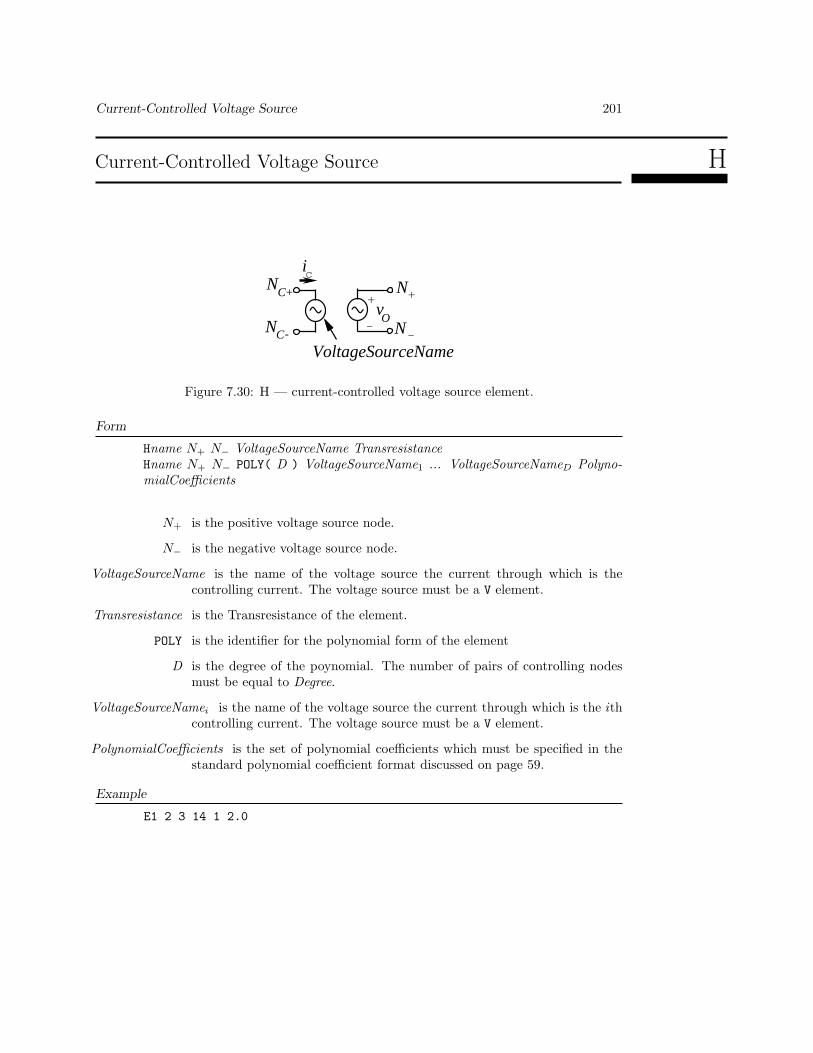
Current-Controlled Voltage Source 201
Current-Controlled Voltage Source H
+
-
ic
+
-
VoltageSourceNameN
NNC+
NC-
vO
Figure 7.30: H — current-controlled voltage source element.
Form
Hname N+ N− VoltageSourceName TransresistanceHname N+ N− POLY( D ) VoltageSourceName1 ... VoltageSourceNameD Polyno-mialCoefficients
N+ is the positive voltage source node.
N− is the negative voltage source node.
VoltageSourceName is the name of the voltage source the current through which is thecontrolling current. The voltage source must be a V element.
Transresistance is the Transresistance of the element.
POLY is the identifier for the polynomial form of the element
D is the degree of the poynomial. The number of pairs of controlling nodesmust be equal to Degree.
VoltageSourceNamei is the name of the voltage source the current through which is the ithcontrolling current. The voltage source must be a V element.
PolynomialCoefficients is the set of polynomial coefficients which must be specified in thestandard polynomial coefficient format discussed on page 59.
Example
E1 2 3 14 1 2.0
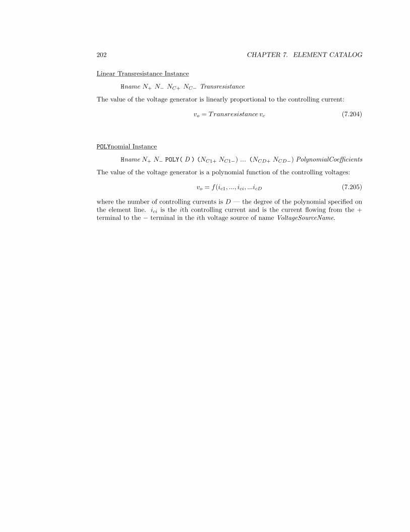
202 CHAPTER 7. ELEMENT CATALOG
Linear Transresistance Instance
Hname N+ N− NC+ NC− Transresistance
The value of the voltage generator is linearly proportional to the controlling current:
vo = Transresistance vc (7.204)
POLYnomial Instance
Hname N+ N− POLY( D ) (NC1+ NC1−) ... (NCD+ NCD−) PolynomialCoefficients
The value of the voltage generator is a polynomial function of the controlling voltages:
vo = f(ic1, ..., ici, ...icD (7.205)
where the number of controlling currents is D — the degree of the polynomial specified onthe element line. ici is the ith controlling current and is the current flowing from the +terminal to the − terminal in the ith voltage source of name VoltageSourceName.

Independent Current Source 203
Independent Current Source I
+
-
N
N
i
Figure 7.31: I — independent current source.
Form
Iname N+ N− [ [DC] [DCvalue]+ [AC [ACmagnitude [ACphase] ] ]+ [DISTOF1 [F1Magnitude [F1Phase] ] ] + [DISTOF2 [F2Magnitude [F2Phase] ]]
Spice3Form
Iname N+ N− [ [DC] [DCvalue]+ [AC [ACmagnitude [ACphase] ] ]+ [TransientSpecification ]+ [DISTOF1 [F1Magnitude [F1Phase] ] ]+ [DISTOF2 [F2Magnitude [F2Phase] ] ]
PSpiceForm
Iname N+ N− [ [DC] [DCvalue] [AC [ACmagnitude [ACphase] ] ]+ [TransientSpecification ]
Example
IBIAS 1 0 1.0MICLOCK 20 5 PULSE(0M 10M 1N 2N 1.5N 21.9N 5N 20N)ISSIGNAL AC 1U 90
204 CHAPTER 7. ELEMENT CATALOG
N+ is the positive current source node. (Current flow is out of the positive tothe negative node
N− is the negative current source node.
DC is the optional keyword for the DC value of the source.
DCvalue is the DC current value of the source.(Units: A; Optional; Default: 0; Symbol: IDC)
AC is the keyword for the AC value of the source.
ACmagnitude is the AC magnitude of the source used during ACanalysis. That is, it is thepeak AC current so that the AC signal is ACmagnitude sin(ωt + ACphase).ACmagnitude is ignored for other types of analyses.(Units: A; Optional; Default: 1; Symbol: IAC)
ACphase is the ac phase of the source. It is used only in AC analysis.(Units: Degrees; Optional; Default: 0; Symbol: φAC)
DISTOF1 is the distortion keyword for distortion component 1 which hass frequencyF1. (see the description of the .DISTO statement on page 74).
F1magnitude is the magnitude of the distortion component at F1. See .DISTOF1 keywordabove.(Units: A; Optional; Default: 1; Symbol: IF1)
F1phase is the phase of the distortion component at F1. See .DISTOF1 keywordabove.(Units: Degrees; Optional; Default: 0; Symbol: φF1)
DISTOF2 is the distortion keyword for distortion component 2 which hass frequencyF2. (see the description of the .DISTO statement on page 74).
F2magnitude is the magnitude of the distortion component at F2. See .DISTOF2 keywordabove.(Units: A; Optional; Default: 1; Symbol: IF2)
F2phase is the phase of the distortion component at F2. See .DISTOF2 keywordabove.(Units: Degrees; Optional; Default: 0; Symbol: φF2)
TransientSpecification is the optional transient specification described more fully below.
Note

Independent Current Source 205
1. The independent current source has three different sets of parameters to describe thesource for DC analysis (see .DC on page 70), AC analysis (see .AC on page 67), andtransient analysis (see .TRAN on page 135). The DC value of the source is used duringbias point evaluation and DC analysis is DCValue. It is also the constant value ofthe current source if no TransientSpecification is supplied. It may also be used inconjunction with the PWL transient specification if a time zero value is not provided aspart of the transient specification. The AC specification, indicated by the keyword ACis independent of the DC parameters and the Transient Specification.
2. The original documentation distributed with Spice2g6 and Spice3 incorrectly statedthat if a TransientSpecification was supplied then the time-zero transient current wasused in DC analysis and in determiniong the operating point.
Transient SpecificationFive transient specification forms are supported: pulse (PULSE), exponential (EXP), sinu-
soidal (SIN), piece-wise linear (PWL), and single-frequency FM (SFFM). The default values ofsome of the parameters of these transient specifications include TSTEP which is the print-ing increment and TSTOP which is the final time (see the .TRAN statement on page 135 forfurther explanation of these quantities). In the following t is the transient analysis time.Exponential:
EXPForm
EXP( I1 I2 [TD1 ] [τ1 ] [TD2 ] [τ2 ] )Name Description Units Default
I1 initial current A REQUIRED
I2 pulsed current A REQUIRED
TD1 rise delay time s 0.0τ1 rise time constant s TSTEPTD2 fall delay time s TD1 +
TSTEPτ2 fall time constant s TSTEP
The exponential transient is a single-shot event specifying two exponentials. The current isI1 for the first TD1 seconds at which it begins increasing exponentially towards I2 with atime constant of τ1 seconds. At time TD2 the current exponentially decays towards I1 witha time constant of τ2. That is,
i =
I1 t ≤ TD1
I1 + (I2 − I1)(1− e(−(t− TD1)/τ1)) TD1 < t ≤ TD2
I1 + (I2 − I1)(1− e(−(t− TD1)/τ1)) + (I1 − I2)(1− e(−(t− TD2)/τ2)) t > TD2
(7.206)Single-Frequency FM:
SFFMForm

206 CHAPTER 7. ELEMENT CATALOG
SFFM( VO VA FC µ FS )
Name Description Units DefaultIO offset current AIA peak amplitude of AC current AFC carrier frequency Hz 1/TSTOPµ modulation index - 0FS signal frequency Hz 1/TSTOP
The single frequency frequency modulated transient response is described by
i = IO + IA sin (2π FCt + µ sin (2πFSt)) (7.207)
Pulse:
PULSEForm
PULSE( V1 V2 [TD ] [TR ] [TF ] [W ] [T ] )

Independent Current Source 207
00.20.40.60.8
11.21.41.61.8
2
0 0.5 1 1.5 2 2.5 3 3.5 4
I2
I1
τ1 τ2
TD1 TD2
t
i
(A)
t (s)
Figure 7.32: Current source exponential (EXP) waveform for EXP(0.1 0.8 1 0.35 2 1)
-1-0.8-0.6-0.4-0.2
00.20.40.60.8
1
0 0.2 0.4 0.6 0.8 1 1.2 1.4 1.6 1.8 2
i
(A)
t (s)
Figure 7.33: Current source single frequency frequency modulation (SFFM) waveform forSFFM(0.2 0.7 4 0.9 1) .
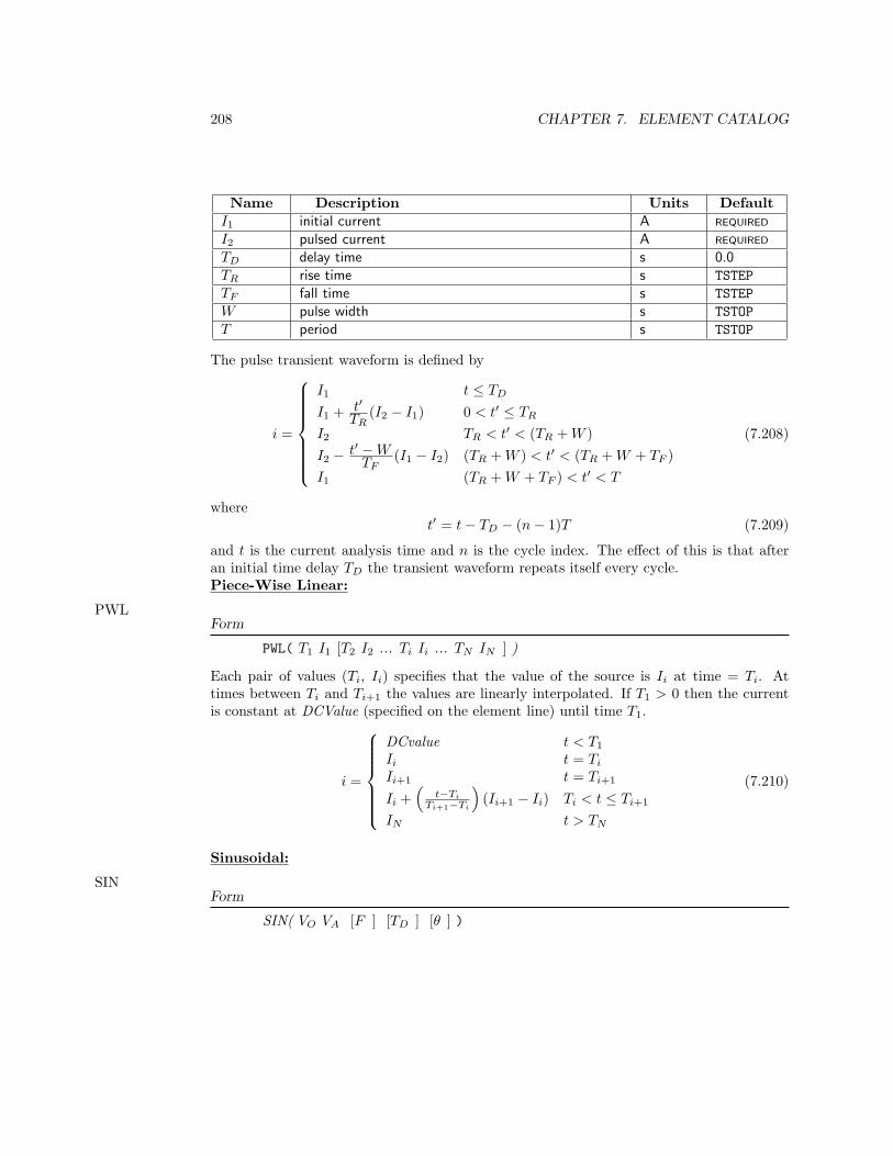
208 CHAPTER 7. ELEMENT CATALOG
Name Description Units DefaultI1 initial current A REQUIRED
I2 pulsed current A REQUIRED
TD delay time s 0.0TR rise time s TSTEPTF fall time s TSTEPW pulse width s TSTOPT period s TSTOP
The pulse transient waveform is defined by
i =
I1 t ≤ TD
I1 + t′TR
(I2 − I1) 0 < t′ ≤ TR
I2 TR < t′ < (TR + W )I2 − t′ −W
TF(I1 − I2) (TR + W ) < t′ < (TR + W + TF )
I1 (TR + W + TF ) < t′ < T
(7.208)
wheret′ = t− TD − (n− 1)T (7.209)
and t is the current analysis time and n is the cycle index. The effect of this is that afteran initial time delay TD the transient waveform repeats itself every cycle.Piece-Wise Linear:
PWLForm
PWL( T1 I1 [T2 I2 ... Ti Ii ... TN IN ] )
Each pair of values (Ti, Ii) specifies that the value of the source is Ii at time = Ti. Attimes between Ti and Ti+1 the values are linearly interpolated. If T1 > 0 then the currentis constant at DCValue (specified on the element line) until time T1.
i =
DCvalue t < T1
Ii t = Ti
Ii+1 t = Ti+1
Ii +(
t−Ti
Ti+1−Ti
)(Ii+1 − Ii) Ti < t ≤ Ti+1
IN t > TN
(7.210)
Sinusoidal:
SINForm
SIN( VO VA [F ] [TD ] [θ ] )

Independent Current Source 209
00.20.40.60.8
11.21.41.61.8
2
0 0.5 1 1.5 2 2.5 3 3.5 4 4.5 5
i
(A)
t (s)
I2
I1
TD←− −→TR
TFW←− −→
←− T −→
Figure 7.34: Current source transient pulse (PULSE) waveform forPULSE(0.3 1.8 1 2.5 0.3 1 0.7)
00.20.40.60.8
11.21.41.61.8
2
0 0.5 1 1.5 2 2.5 3 3.5 4 4.5 5
•
IDC
(T1, I1)
i
(A)
t (s)
(T2, I2)
(T3, I3) (Ti, Ii)
(Ti+1, Ii+1)
(TN , IN )
Figure 7.35: Current source transient piece-wise linear (PWL) waveform forPWL(1 0.25 1 1 2 0.5 . . . 3 0.5 4 1 . . . 4.5 1.25 . . .) with DCValue = 0.25.

210 CHAPTER 7. ELEMENT CATALOG
PSpiceForm
SIN( VO VA [F ] [TD ] [θ φ ] )
PSpice92Form
SIN( VO VA [F ] [TD ] [θ φ ] )
Name Description Units DefaultIO current offset A REQUIRED
IA current amplitude A REQUIRED
F frequency Hz 1/TSTOPTD time delay s 0Θ damping factor 1/s 0φ phase degree 0
The sinusoidal transient waveform is defined by
i =
I0 t ≤ TD
I0 + I1e−[(t− TD)Θ] sin 2π[F (t− TD) + φ/360] t > TD
(7.211)
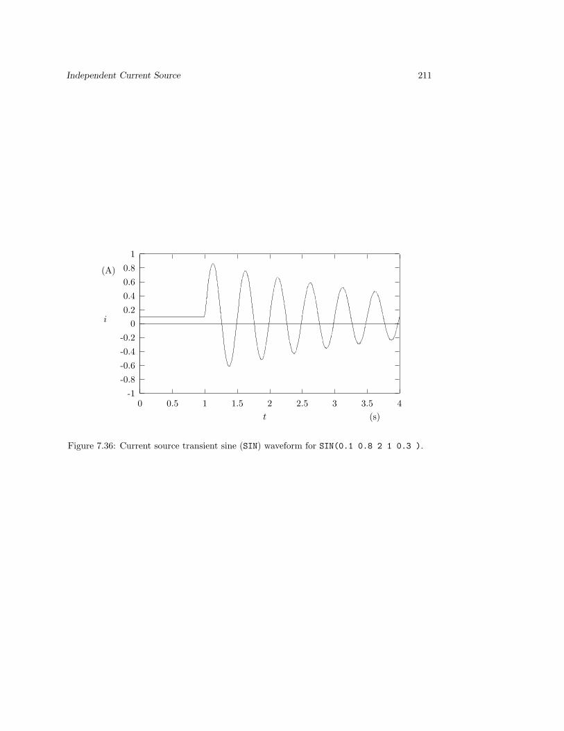
Independent Current Source 211
-1-0.8-0.6-0.4-0.2
00.20.40.60.8
1
0 0.5 1 1.5 2 2.5 3 3.5 4
i
(A)
t (s)
Figure 7.36: Current source transient sine (SIN) waveform for SIN(0.1 0.8 2 1 0.3 ).
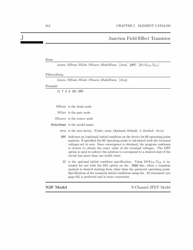
212 CHAPTER 7. ELEMENT CATALOG
J Junction Field-Effect Transistor
Form
Jname NDrain NGate NSource ModelName [Area] [OFF] [IC=VDS , VGS ]
PSpiceForm
Jname NDrain NGate NSource ModelName [Area]
Example
J1 7 2 3 JM1 OFF
NDrain is the drain node
NGate is the gate node
NSource is the source node
ModelName is the model name
Area is the area factor. (Units: none; Optional; Default: 1; Symbol: Area)
OFF indicates an (optional) initial condition on the device for DC operating pointanalysis. If specified the DC operating point is calculated with the terminalvoltages set to zero. Once convergence is obtained, the program continuesto iterate to obtain the exact value of the terminal voltages. The OFFoption is used to enforce the solution to correspond to a desired state if thecircuit has more than one stable state.
IC is the optional initial condition specification. Using IC=VDS , VGS is in-tended for use with the UIC option on the .TRAN line, when a transientanalysis is desired starting from other than the quiescent operating point.Specification of the transient initial conditions using the .IC statement (seepage 83) is preferred and is more convenient.
NJF Model N-Channel JFET Model
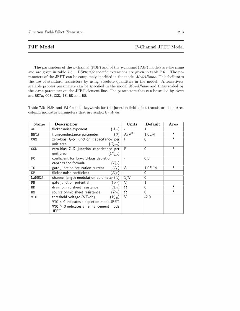
Junction Field-Effect Transistor 213
PJF Model P-Channel JFET Model
The parameters of the n-channel (NJF) and of the p-channel (PJF) models are the sameand are given in table 7.5. PSpice92 specific extensions are given in table 7.6. The pa-rameters of the JFET can be completely specified in the model ModelName. This facilitatesthe use of standard transistors by using absolute quantities in the model. Alternativelyscalable process parameters can be specified in the model ModelName and these scaled bythe Area parameter on the JFET element line. The parameters that can be scaled by Areaare BETA, CGS, CGD, IS, RD and RS.
Table 7.5: NJF and PJF model keywords for the junction field effect transistor. The Areacolumn indicates parameters that are scaled by Area.
Name Description Units Default AreaAF flicker noise exponent (AF ) - 1
BETA transconductance parameter (β) A/V2 1.0E-4 *CGS zero-bias G-S junction capacitance per
unit area (C ′GS)F 0 *
CGD zero-bias G-D junction capacitance perunit area (C ′GD)
F 0 *
FC coefficient for forward-bias depletioncapacitance formula (FC)
- 0.5
IS gate junction saturation current (IS) A 1.0E-14 *KF flicker noise coefficient (KF ) - 0LAMBDA channel length modulation parameter (λ) 1/V 0PB gate junction potential (φJ) V 1RD drain ohmic sheet resistance (RD) Ω 0 *RS source ohmic sheet resistance (RS) Ω 0 *VTO threshold voltage (VT-oh) (VT0)
VTO < 0 indicates a depletion mode JFETVTO ≥ 0 indicates an enhancement modeJFET
V -2.0

214 CHAPTER 7. ELEMENT CATALOG
Table 7.6: JFET model keyword: PSpice92 extenions.
Name Description Units DefaultBETATC temperature coefficient of the transconductance pa-
rameter BETA (TC,β)%/C 0
M gate p-n junction grading coefficient (M) - 0.5VTOTC temperature coefficient of threshold voltage VTO
(TC,V T0)V/C 0

Junction Field-Effect Transistor 215
Figure 7.37: J — Junction field effect transistor element: (a) n channel JFET; (b) p channelJFET.
216 CHAPTER 7. ELEMENT CATALOG
Figure 7.38: Schematic of the JFET model. VGS , VDS , and VGD are intrinsic gate-source,drain-source and gate-drain voltages between the internal gate, drain, and source terminalsdesignated G, D, and C respectively.
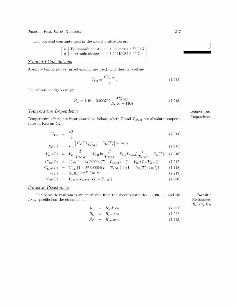
Junction Field-Effect Transistor 217
JThe physical constants used in the model evaluation are
k Boltzman’s constant 1.3806226 10−23 J/Kq electronic charge 1.6021918 10−19 C
Standard Calculations
Absolute temperatures (in kelvins, K) are used. The thermal voltage
VTH =kTNOM
q. (7.212)
The silicon bandgap energy
EG = 1.16− 0.0007024T 2
NOM
TNOM + 1108. (7.213)
Temperature Dependence TemperatureDependenceTemperature effects are incorporated as follows where T and TNOM are absolute tempera-
tures in Kelvins (K).
VTH =kT
q(7.214)
IS(T ) = ISe
(Eg(T ) T
TNOM− EG(T )
)/(nVTH)
(7.215)
VBI(T ) = VBIT
TNOM− 3VTH ln
T
TNOM+ EG(TNOM)
T
TNOM− EG(T ) (7.216)
C ′GS(T ) = C ′GS1 + M [0.0004(T − TNOM) + (1− VBI(T )/VBI)] (7.217)C ′GD(T ) = C ′GD1 + M [0.0004(T − TNOM) + (1− VBI(T )/VBI)] (7.218)
β(T ) = β1.01TC,β(T−TNOM) (7.219)VT0(T ) = VT0 + TC,V T0 (T − TNOM) (7.220)
Parasitic Resistances
The parasitic resistances are calculated from the sheet resistivities RS, RG, RD, and the ParasiticResistancesRS RG RD
Area specified on the element line.
RS = R′SArea (7.221)RG = R′GArea (7.222)RD = R′DArea (7.223)
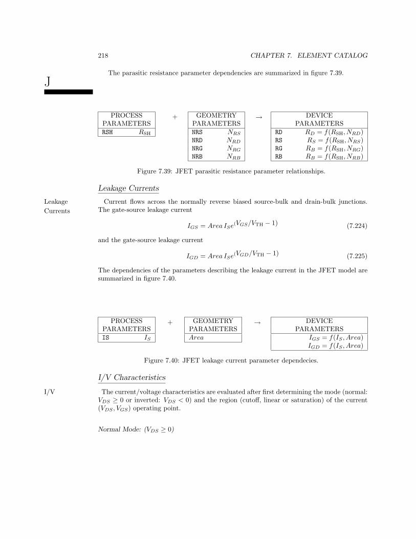
218 CHAPTER 7. ELEMENT CATALOG
JThe parasitic resistance parameter dependencies are summarized in figure 7.39.
PROCESSPARAMETERSRSH RSH
+ GEOMETRYPARAMETERSNRS NRS
NRD NRD
NRG NRG
NRB NRB
→ DEVICEPARAMETERS
RD RD = f(RSH, NRD)RS RS = f(RSH, NRS)RG RB = f(RSH, NRG)RB RB = f(RSH, NRB)
Figure 7.39: JFET parasitic resistance parameter relationships.
Leakage Currents
Current flows across the normally reverse biased source-bulk and drain-bulk junctions.LeakageCurrents The gate-source leakage current
IGS = Area ISe(VGS/VTH − 1) (7.224)
and the gate-source leakage current
IGD = Area ISe(VGD/VTH − 1) (7.225)
The dependencies of the parameters describing the leakage current in the JFET model aresummarized in figure 7.40.
PROCESSPARAMETERSIS IS
+ GEOMETRYPARAMETERSArea
→ DEVICEPARAMETERS
IGS = f(IS , Area)IGD = f(IS , Area)
Figure 7.40: JFET leakage current parameter dependecies.
I/V Characteristics
The current/voltage characteristics are evaluated after first determining the mode (normal:I/VVDS ≥ 0 or inverted: VDS < 0) and the region (cutoff, linear or saturation) of the current(VDS , VGS) operating point.
Normal Mode: (VDS ≥ 0)
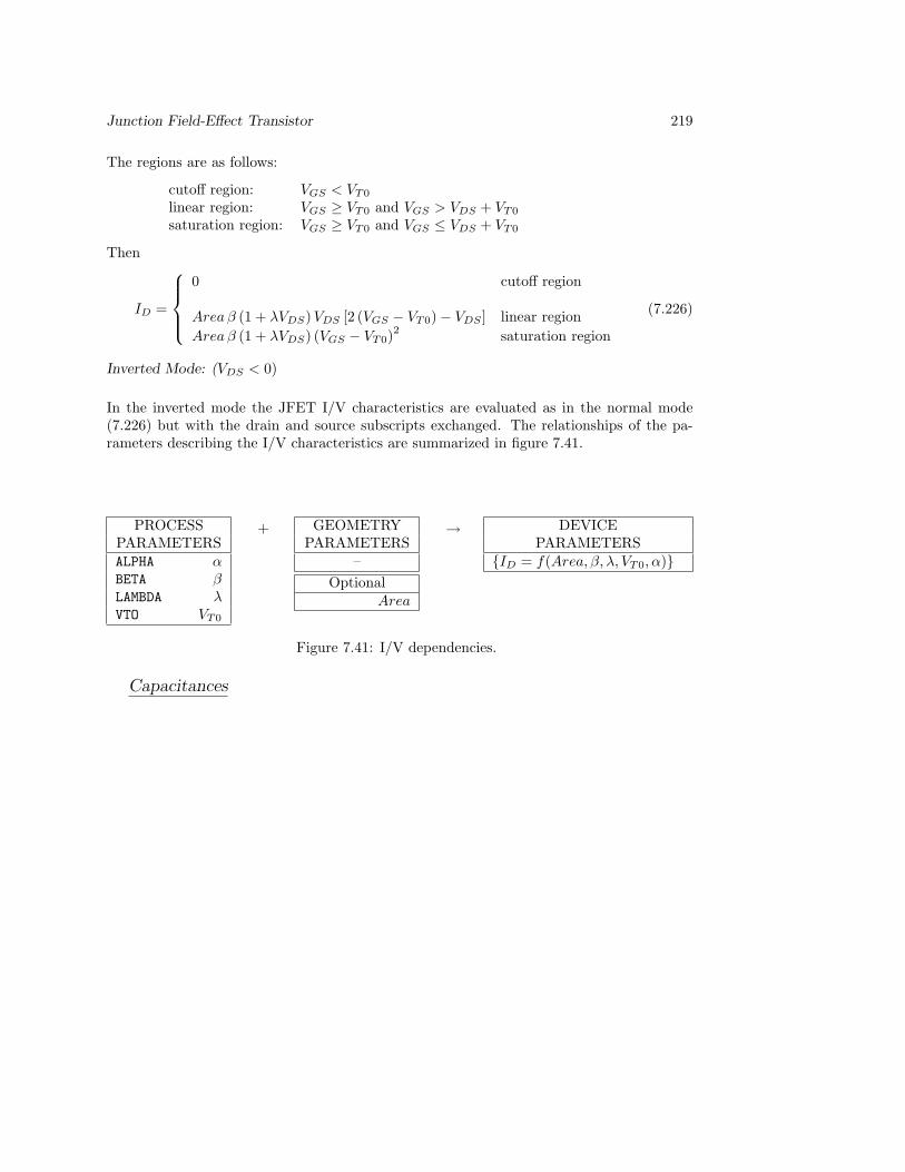
Junction Field-Effect Transistor 219
The regions are as follows:
cutoff region: VGS < VT0
linear region: VGS ≥ VT0 and VGS > VDS + VT0
saturation region: VGS ≥ VT0 and VGS ≤ VDS + VT0
Then
ID =
0 cutoff region
Area β (1 + λVDS)VDS [2 (VGS − VT0)− VDS ] linear regionArea β (1 + λVDS) (VGS − VT0)
2 saturation region
(7.226)
Inverted Mode: (VDS < 0)
In the inverted mode the JFET I/V characteristics are evaluated as in the normal mode(7.226) but with the drain and source subscripts exchanged. The relationships of the pa-rameters describing the I/V characteristics are summarized in figure 7.41.
PROCESSPARAMETERSALPHA αBETA βLAMBDA λVTO VT0
+ GEOMETRYPARAMETERS
–Optional
Area
→ DEVICEPARAMETERS
ID = f(Area, β, λ, VT0, α)
Figure 7.41: I/V dependencies.
Capacitances
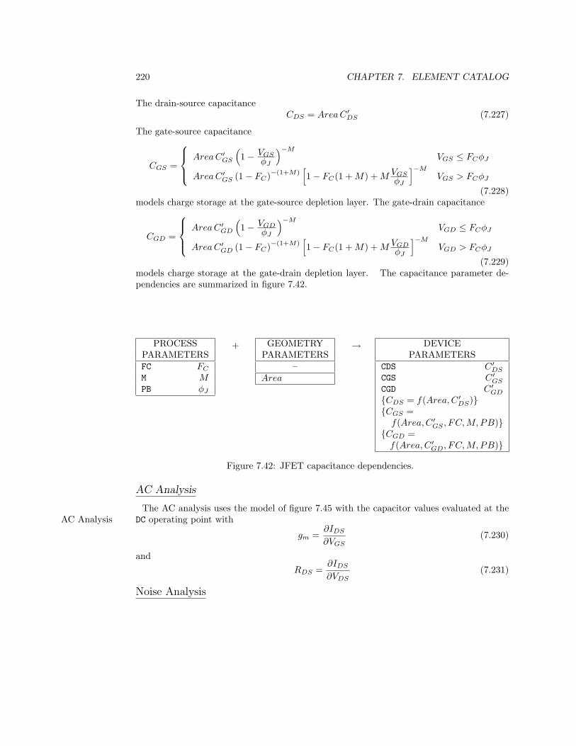
220 CHAPTER 7. ELEMENT CATALOG
The drain-source capacitanceCDS = AreaC ′DS (7.227)
The gate-source capacitance
CGS =
Area C ′GS
(1− VGS
φJ
)−M
VGS ≤ FCφJ
Area C ′GS (1− FC)−(1+M)[1− FC(1 + M) + M VGS
φJ
]−M
VGS > FCφJ
(7.228)models charge storage at the gate-source depletion layer. The gate-drain capacitance
CGD =
AreaC ′GD
(1− VGD
φJ
)−M
VGD ≤ FCφJ
AreaC ′GD (1− FC)−(1+M)[1− FC(1 + M) + M VGD
φJ
]−M
VGD > FCφJ
(7.229)models charge storage at the gate-drain depletion layer. The capacitance parameter de-pendencies are summarized in figure 7.42.
PROCESSPARAMETERSFC FC
M MPB φJ
+ GEOMETRYPARAMETERS
–Area
→ DEVICEPARAMETERS
CDS C ′DS
CGS C ′GS
CGD C ′GD
CDS = f(Area, C ′DS)CGS =
f(Area, C ′GS , FC, M, PB)CGD =
f(Area,C ′GD, FC, M, PB)
Figure 7.42: JFET capacitance dependencies.
AC Analysis
The AC analysis uses the model of figure 7.45 with the capacitor values evaluated at theAC Analysis DC operating point with
gm =∂IDS
∂VGS(7.230)
andRDS =
∂IDS
∂VDS(7.231)
Noise Analysis
Junction Field-Effect Transistor 221
The JFET noise model accounts for thermal noise generated in the parasitic resistances andNoise Analysisshot and flicker noise generated in the drain source current generator. The rms (root-mean-square) values of thermal noise current generators shunting the four parasitic resistance RD,RG and RS are
In,D =√
4kT/RD A/√
Hz (7.232)
In,S =√
4kT/RS A/√
Hz (7.233)
Shot and flicker noise are modeled by a noise current generator in series with the drain-sourcecurrent generator. The rms value of this noise generator is
In,DS =(I2SHOT,DS + I2
FLICKER,DS
)(7.234)
ISHOT,DS =
√4kTgm
23
A/√
Hz A/√
Hz (7.235)
IFLICKER,DS =
√KF IAF
DS
fA/√
Hz (7.236)
where the transconductancegm =
∂IDS
∂VGS(7.237)
is evaluated at the DC operating point, and f is the analysis frequency.

222 CHAPTER 7. ELEMENT CATALOG
K Mutual Inductor
n1
n2
n3
n4n2
n1n1
n2
LLx y
Figure 7.43: K — Mutual inductor element.
Form
Kname Lname1 Lname2 CouplingValue
PSpiceForm
Kname Lname1 Lname2 [... LnameN ] CouplingValue
Kname Lname1 [Lname2 ... LnameN ] CouplingValue [ [ModelName [size ] ]

Mutual Inductor 223
Lname1 is the name of the first inductor of the coupled inductor list. The first nodeof Lname1 is dotted using the dot convention. In the mutual coupled induc-tor model (the default model) the value of Lname1 is the self inductance L1.In the transformer CORE model (which is used if a ModelName is supplied)the value of Lname1 is the number of turns N1. (Note, ModelName can notbe specified with the Spice2g6 and Spice3 simulators.)(Required)
Lname2 is the name of the second inductor in the coupled inductor list. The firstnode of Lname1 is dotted using the dot convention. In the mutual coupledinductor model the value of Lname1 is the self inductance L2. In the trans-former CORE model (which is used if a ModelName is supplied the value ofLname2 is the number of turns N2.(Spice2g6 and Spice3: Required.)(PSpice: Required if Modelname not supplied; Optional if Modelname sup-plied.)
LnameN is the name of Nth inductor in the coupled inductor list. The first node ofLnameN is dotted using the dot convention. In the mutual inductor modelthe value of LnameN is the self inductance LN . In the transformer COREmodel (which is used if a ModelName is supplied the value of Lname2 is thenumber of turns NN .Not valid in Spice2g6 or Spice3 for N > 2.(PSpice: Optional if Modelname supplied.)
CouplingValue is the coefficient of mutual coupling of the inductors.(Units: none; Required; Symbol: KCOUPLING; 0 < KCOUPLING ≤ 1)
ModelName is the optional model name. PSpice only.
Size is the size scaling factor. It scales the magnetic cross-section and representsthe number of lamination layers.(Units: none; Optional; Default: 1; Symbol: Size)
Example
K43 LAA LBB 0.999KXFRMR L1 L2 0.87
PSpice Example
KTFMR LAA LBB LCC LDD TRANSFORMER 2.5
Model Type
224 CHAPTER 7. ELEMENT CATALOG
IND PSpice only
Note
1. The mutual coupled inductor model represents coupled inductors by self inductancesLi and mutual inductances Mij . This is the model used in Spice2g6 and spicthreeand in PSpice if a CORE model is not supplied. Here Li is the self inductance of theith inductor element and Mij is the mutual inductance of the ith and jth inductorelements. The mathematical model of the coupled element consists of voltage sourcescontrolled by the time derivatives of current. If two inductors are coupled
V1 = L1dI1
dt+ M12 +
dI2
dt(7.238)
andV2 = L2
dI2
dt+ M21 +
dI1
dt(7.239)
If N inductors are coupled, as supported in PSpice , the mathematical model is
Note

Mutual Inductor 225
Vi = LidIi
dt+
N∑
j = 1j 6= i
MijdIj
dt(7.240)
2 The mutual inductance Mij is determined from the self-inductances Li and Lj of theinductors and the coupling coefficient KCOUPLING supplied as an element parameterby
KCOUPLING =
√Mij
LiLj(7.241)
KCOUPLING may have any value between 0 and 1 including 1. Ferrite core providesalmost ideal coupling with K = 0.999 or higher.
3 In Spice2g6 and Spice3 a transformer with several coils must be represented byseveral K elements. For example, a transformer with one primary and two secondariesis specified as
* PRIMARYL1 1 2 100U* FIRST SECONDARYL2 3 4 100U* SECOND SECONDARYL3 5 6 100U* TRANSFORMERK1 L1 L2 0.999K2 L1 L3 0.999K2 L2 L3 0.999
4 In PSpice the transformer above can be either represented using the Spice2g6 andSpice3 format above or by the more compact format
* PRIMARYL1 1 2 100U* FIRST SECONDARYL2 3 4 100U* SECOND SECONDARYL3 5 6 100U* TRANSFORMERK1 L1 L2 L3 0.999
CORE Model PSpice Only Magnetic Core Model
FormCORE.MODEL ModelName CORE( [ [keyword = value] ... ] )
226 CHAPTER 7. ELEMENT CATALOG
Example
.MODEL TRANSFORMER CORE(AREA=1 PATH=9.8 GAP=0.1 MS=1.250M)
Model KeywordsName Description Units DefaultA shape parameter (A) A/M 103
ALPHA (α) interdomain coupling parameter - 0.001AREA mean magnetic crossection (Area) cm2 0.1GAMMA domain damping parameter. (γ) - ∞C domain flexing parameter (C) - 0.2GAP effective air-gap length (LGAP) cm 0K domain anisotopy parameter (pinning constant) (K) A/M 500MS magnetization saturation (MS) A/M 106
PACK pack (stacking) factor (FPACK) cm 0PATH mean magnetic path length in the core (LPATH) cm 1
The CORE model models a transformer core. It is assumed that the model parameterswere determined or measured at the nominal temperature TNOM (default 27C) specified inthe most recent .OPTIONS statement preceeding the .MODEL statement.
The CORE model uses the Jiles-Atherton model described in [25]. This model is basedon domain wall motion and includes flexing of the domain wall, interdomain coupling,coercivity, remanence and magnetic saturation. Hysteresis due to domain wall pinning atdefect sites is modeled. This impedance to domain wall motion dominates the characteristicsof magnetic devices.
As with the default mutually coupled inductor model, the CORE model calculates the volt-age across the ith set of windings from the total ampere turns which is the magnetomotiveforce MMF . Thus
Vi =dφi
dt= f(MMF ) (7.242)
where
Mutual Inductor 227
KMMF =N∑
j=1
NjIj (7.243)
Here the number of turns of the jth winding, Nj , is the “InductanceValue” of Lj the nameof which is the jth Lname given on the K element line. Ii is the curent flowing through theith winding. ATURNS produces the magnetic field HCORE in the core. This in turn producesthe B field. The B field is proportional to the flux, in the core and hence to the voltage Vi.The relationship between B and H in the core is nonlinear and hysteretic. The airgap alsoaffects the B-H relationship.
Air-Gap Effect
Along the complete magnetic path
HCORELPATH + HGAPLGAP = MMF (7.244)
where HCORE is the magnetic field in the core and HGAP is the magnetic field in the airgap. LPATH and LGAP are the model parameters PATH and GAP. If the air gap is small thenall of the flux in the core passes through the air gap so that BGAP = BCORE. In the air-gapthe magnetization is negligible so that BGAP = HGAP
This leads to a relationship beween the B and H fields in the core:
HCORELPATH + BCORELGAP = MMF (7.245)
It is a simple matter to solve for BCORE and HCORE if LGAP =0 as then
HCORE =MMF
LPATH(7.246)
If LGAP > 0 then (7.245) must be solved in conjunction with the relationship betweenHCORE and magnetization M in the core. This relationship is based on the theory ofloosely coupled domains developed by Jiles and Atherton.Jiles-Atherton Model
228 CHAPTER 7. ELEMENT CATALOG
The B-H curve of a magnetic material biased by AC and DC magnetic fields is called theanhysteric and is mathematically described by the Jiles-Atherton model. This model deter-mines an anhysteric magnetization MAN which is related to the saturation magnetizationMS by
MAN = MS
[coth
(HEFF
SizeA
)− Size A
HEFF
](7.247)
where A is the shape parameter and the effective field in the core
HEFF = HCORE + αMAN (7.248)
Here H is the magnetizing influence. Domain wall flux is magnetic current which is propor-tional to the change in magnetization. The change in magnetization consists of a reversiblecomponent due to flexing of the domain walls and an irreversible component due to move-ment of domain walls from one pinning location to another. Energy is dissipated (hencethe motion is irreversible) in moving the domain wall from one pinning location to anotherbut energy is stored (hence reversible) when the domain wall flexs. This is mathematiclymodeled by
dM
dHCORE=
(dM
dHCORE
)
REVERSIBLE
+(
dM
dHCORE
)
IRREVERSIBLE
(7.249)
where the reversible component(
dM
dHCORE
)
REVERSIBLE
= Cd(MAN −M)
dH(7.250)
and the irreversible component(
dM
dHCORE
)
IRREVERSIBLE
=MAN −M
K(7.251)
where K is the pinning energy per volume and is akin to mechanical drag. M and HCORE
are found by solving (7.249) and (7.245) simultaneously.The small signal relative permeability of the core is
µr =
[(dM
dHCORE+ 1
)FPACK
]−1
+LGAP
LPATH
−1
(7.252)
and the flux passing through the ith winding is
φi = µ0(M + HCORE)NiFPACK Size Area (7.253)
The voltage across the ith winding is then found as
Vi =dφi
dt(7.254)
AC Analysis

Mutual Inductor 229
For AC analysis the mutual inductor model is used even if a CORE model is specified.This allows a different coefficient of mutual coupling to be used in AC analysis than wouldotherwise be determined by nonlinear model evaluation.
Noise Analysis
The K element does not contribute to noise.
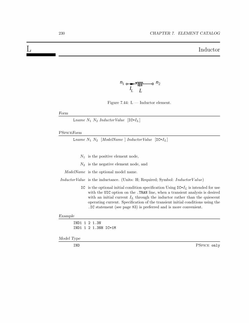
230 CHAPTER 7. ELEMENT CATALOG
L Inductor
n1 n2
LIL
Figure 7.44: L — Inductor element.
Form
Lname N1 N2 InductorValue [IC=IL ]
PSpiceForm
Lname N1 N2 [ModelName ] InductorValue [IC=IL ]
N1 is the positive element node,
N2 is the negative element node, and
ModelName is the optional model name.
InductorValue is the inductance. (Units: H; Required; Symbol: InductorV alue)
IC is the optional initial condition specification Using IC=IL is intended for usewith the UIC option on the .TRAN line, when a transient analysis is desiredwith an initial current IL through the inductor rather than the quiescentoperating current. Specification of the transient initial conditions using the.IC statement (see page 83) is preferred and is more convenient.
Example
IND1 1 2 1.3NIND1 1 2 1.3NH IC=1M
Model Type
IND PSpice only

Inductor 231
INDIND Model PSpice Only Inductor Model
Form
.MODEL ModelName IND( [ [keyword = value] ... ] )
Example
.MODEL SMALLIND IND(L=4.5 IL1=0.1 IL2 = 0.01 TC1=0.01 TC2=0.001)
Model KeywordsName Description Units DefaultL inductance multiplier (LMULTIPLIER) - 1IL1 linear current coefficient (IC1) 1/A 0IL2 quadratic current coefficient (IC2) 1/A 0TC1 linear temperature coefficient (TC1) 1/C 0TC2 quadratic temperature coefficient (TC1)
C−2 0
The PSpice inductance model is a nonlinear temperature dependent inductor model. Itis assumed that the model parameters were determined or measured at the nominal tem-perature TNOM (default 27C) specified in the most recent .OPTIONS statement precedingthe .MODEL statement.
The inductance is
L = InductorV alue LMULTIPLIER
[1 + IL1IL + IL2I
2L
]
× [1 + TC1(T − TNOM) + TC2(T − TNOM )2
](7.255)
where IL is the current flowing through the inductor as in figure 7.44 and T is the currenttemperature.
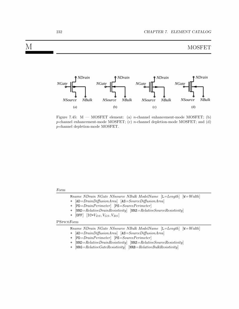
232 CHAPTER 7. ELEMENT CATALOG
M MOSFET
NDrain
NSource
NGate
NBulk
NDrain
NSource
NGate
NBulk
NDrain
NSource
NGate
NBulk
NDrain
NSource
NGate
NBulk
(a) (b) (c) (d)
Figure 7.45: M — MOSFET element: (a) n-channel enhancement-mode MOSFET; (b)p-channel enhancement-mode MOSFET; (c) n-channel depletion-mode MOSFET; and (d)p-channel depletion-mode MOSFET.
Form
Mname NDrain NGate NSsource NBulk ModelName [L=Length] [W=Width]+ [AD=DrainDiffusionArea] [AS=SourceDiffusionArea]+ [PD=DrainPerimeter] [PS=SourcePerimeter]+ [NRD=RelativeDrainResistivity] [NRS=RelativeSourceResistivity]+ [OFF] [IC=VDS , VGS , VBS ]
PSpiceForm
Mname NDrain NGate NSsource NBulk ModelName [L=Length] [W=Width]+ [AD=DrainDiffusionArea] [AS=SourceDiffusionArea]+ [PD=DrainPerimeter] [PS=SourcePerimeter]+ [NRD=RelativeDrainResistivity] [NRS=RelativeSourceResistivity]+ [NRG=RelativeGateResistivity] [NRB=RelativeBulkResistivity]

MOSFET 233
NDrain is the drain node.
NGate is the gate node.
NSource is the source node.
NBulk is the bulk or substrate node.
ModelName is the model name.
L is the channel lateral diffusion Length.(Units: m; Optional; Symbol: L; The default is version dependent.Spice2g6 and Spice3 Default: the length DEFL most recently specified ina .OPTION statement which in-turn defaults to 100 µm (100U); PSpiceDefault: the length L – length specified in model ModelName which in turndefaults to the default length DEFL most recently specified in a .OPTIONstatement which in-turn defaults to 100 µm (100U).)
W is the channel lateral diffusion Width.(Units: m; Optional; Symbol: W ; The default is version dependent.Spice2g6 and Spice3 Default: the width DEFW most recently specified ina .OPTION statement which in-turn defaults to 100 µm (100U);PSpice Default: the width W – width specified in model ModelName whichin turn defaults to the default width DEFW most recently specified in a.OPTION statement which in-turn defaults to 100 µm (100U).)
AD is the area of the drain diffusion (DrainDiffusionArea). The default is DEFADmost recently specified in a .OPTIONS statement.(Units: m2; Optional; Default: DEFAD; Symbol: AD)
AS is the area of the source diffusion (SourceDiffusionArea). The default isDEFAS most recently specified in a .OPTIONS statement.(Units: m2; Optional; Default: DEFAS; Symbol: AS)
PD is the perimeter of the drain junction (DrainPerimeter).(Units: m; Optional; Default: 0; Symbol: PD)
PS is the perimeter of the source junction (SourcePerimeter).(Units: m; Optional; Default: 0; symbol: PS)
NRD is the relative resistivity in squares of the drain region (RelativeDrainRe-sistivity). The sheet resistance RSH specified in the model ModelName isdivided by this factor to obtain the parasitic drain resistance.(Units: squares; Optional; Default: 0; Symbol: NRD)
NRS is the relative resistivity in squares of the source region (RelativeSourceRe-sistivity). The sheet resistance RSH specified in the model ModelName isdivided by this factor to obtain the parasitic source resistance.(Units: squares; Optional; Default: 0; Symbol: NRS)
NRG is the relative resistivity in squares of the gate region (RelativeGateResistiv-ity). The sheet resistance RSH specified in the model ModelName is dividedby this factor to obtain the parasitic gate resistance.(Units: squares; Optional; Default: 0; Symbol: NRG)
NRB is the relative resistivity in squares of the bulk (substrate) region (Rela-tiveBulkResistivity). The sheet resistance RSH specified in the model Mod-elName is divided by this factor to obtain the parasitic bulk resistance.(Units: squares; Optional; Default: 0; Symbol: NRB)
OFF indicates an (optional) initial condition on the device for DC analysis. Ifspecified the DC operating point is calculated with the terminal voltages setto zero. Once convergence is obtained, the program continues to iterate toobtain the exact value of the terminal voltages. The OFF option is used toenforce the solution to correspond to a desired state if the circuit has morethan one stable state.
IC is the optional initial condition specification. Using IC=VDS , VGS , VBS isintended for use with the UIC option on the .TRAN line, when a transientanalysis is desired starting from other than the quiescent operating point.Specification of the transient initial conditions using the .IC statement (seepage 83) is preferred and is more convenient.
Example

234 CHAPTER 7. ELEMENT CATALOG
M1 24 2 0 20 TYPE1M31 2 17 6 10 MODM L=5U W=2UM1 2 9 3 0 MOD1 L=10U W=5U AD=100P AS=100P PD=40U PS=40U
Note
1. The parameters of a MOSFET can be completely specified in the model ModelName.This facilitates the use of standard transistors by using absolute quantities in themodel. Alternatively scalable process parameters can be specified in the model Mod-elName and these scaled by geometric parameters on the MOSFET element line.
2. In Spice2g6 and Spice3 the width W can not be specified in the model statement. Forthese simulators absolute device parameters must be specified in the model statementif parameters are not input on the element line.
Model Type
NMOSPMOS
Example
M1 5 5 1 1 PCH L=2.0U W=20U AD=136P AS=136P···.MODEL PCH PMOS LEVEL=2 VTO=-0.76 GAMMA=0.6 CGSO=3.35E-10+ CGDO=3.35E-10 CJ=4.75E-4 MJ=0.4 TOX=225E-10 NSUB=1.6E16+ XJ=0.2E-6 LD=0 UO=139 UEXP=0 KF=5E-30 LAMBDA=0.02
NMOS Model N-CHANNEL MOSFET MODEL
PMOS Model P-CHANNEL MOSFET MODEL
MOSFET 235
NMOSPMOS Two groups of model parameters define the linear and nonlinear elements of the MOS-
FET models. One group defines absolute quantities and another group defines quantitiesthat are multiplied by scaling parameters related to area and dimension which are specifiedon the element line. This enables the MOSFET element to be used in two ways. Usingthe absolute quantities the characteristics of a device can be defined independent of theparameters on the element line. Thus the model of a standard transistor, perhaps residentin a library, can be used without user-knowledge required. Using the scalable quantities theparameters of a fabrication process can be defined in the model statement and scaling pa-rameters such as the lateral diffusion length (specified by L) and the lateral diffusion width(specified by W), and the drain and source diffusion areas (specfified by AD and AS specifiedon the element line). An example is the specification of the drain-bulk saturation currentID,SAT. This parameter can be specified by the absolute parameter IS specified by the ISmodel keyword. It can also be determined as IS = JS ·AD using the scalable parameter JS
specified by the JS model keyword and AD specified by the AD element keyword.Spice provides four MOSFET device models. The first three models, known as LEVELs
1, 2 and 3 differ in the formulation of the I-V characteristic. The fourth model, known asthe BSIM model, uses a completely different formulation utilizing extensive semiconductorparameters. The parameter LEVEL specifies the model to be used:
236 CHAPTER 7. ELEMENT CATALOG
LEVEL = 1 → “Shichman-Hodges”, MOS1This model was the first SPICE MOSFET model and was devel-oped in 1968 [3]. It is an elementary model and has a limited scalingcapability. It is applicable to fairly large devices with gate lengthsgreater than 4 µm. Its main attribute is that only a few parametersneed be specified and so it is good for preliminary analyses.
LEVEL = 2 → MOS2This is an analytical model which uses a combination of processingparameters and geometry. The major development over the LEVEL1 model is improved treatment of the capacitances due to the chan-nel charge. [4–6]. The model dates from 1980 and is applicable forchanel lengths of 2 µm and higher [7].The LEVEL 2 model has convergence problems and is slower andless accurate than the LEVEL 3 model.
LEVEL = 3 → MOS3This is a semi-empirical model developed in 1980 [7]. It is also usedfor gate lengths of 2 µm and more. The parameters of this modelare determined by experimental characterization and so it is moreaccurate than the LEVEL 1 and 2 models that use the more indirectprocess parameters.
LEVEL = 4 → BSIM or BSIM1The BSIM model is an advanced empirical model which uses pro-cess information and a larger number of parameters (more than 60)to describe the operation of devices with gate lengths as short as1 µm. It was developed in 1985 [9].
Other MOSFET models or LEVELs are available in various versions of SPICE. These LEVELsare optimized for MOSFETs fabricated in a particular foundary or provide a proprietaryedge for the advanced commercial SPICE programs. The reader interested in moreadvanced MOSFET models is refered to [8].
LEVEL 1, 2 and 3 MOSFET models.

MOSFET 237
Figure 7.46: Schematic of LEVEL 1, 2 and 3 MOSFET models. VGS , VDS , VGD, VGB , VDB
and VBS are voltages between the internal gate, drain, bulk and source terminals designatedG, D, B and C respectively.
LEVEL 1LEVEL 2LEVEL 3
The LEVEL 1, 2 and 3 models have much in common. These models evaluate the junctiondepletion capacitances and parasitic resistances of a transistor in the same way. They differin the procedure used to evaluate the overlap capacitances (CGD, CGS and CGB) and thatused to determine the current-voltage characteristics of the active region of a transistor. Theoverlap capacitances model charge storage as nonlinear thin-oxide capacitance distributedamong the gate, source drain and bulk regions. These capacitances are important in describ-ing the operation of MOSFETs. The LEVEL 1, 2 and 3 models are intimately intertwined ascombinations of parameters can result in using equations from more than one model. TheLEVEL parameter resolves conflicts when there is more than one way to calculate the tran-sistor characteristics with the parameters specified by the user. Antognetti and Massobrioprovide a comprehensive discussion of the development of the LEVEL 1, 2 and 3 models [2].

238 CHAPTER 7. ELEMENT CATALOG
The parameters of the LEVEL 1, 2 and 3 models are given in table 7.7. Parameterextensions for PSpice are given in table 7.8. It is assumed that the model parameterswere determined or measured at the nominal temperature TNOM (default 27C) specifiedin the most recent .OPTIONS statement preceeding the .MODEL statement. In PSpice thisis overwritten by the T MEASURED parameter. Most of the parameters have default values.Those parameters that have INFERRED defaults are calculated from other parameters.
Table 7.7: MOSFET model keywords for LEVELs 1, 2, 3.
Name Description Units DefaultAF flicker noise exponent (AF ) - 1CBD zero-bias B-D junction capacitance (C ′BD) F 0CBS zero-bias B-S junction capacitance (C ′BS) F 0CGBO gate-bulk overlap capacitance per meter of channel
length(PARASITIC) (CGBO)
F/m 0
CGDO gate-drain overlap capacitance per meter of channelwidth(PARASITIC) (CGDO)
F/m 0
CGSO gate-source overlap capacitance per meter of channelwidth(PARASITIC) (CGSO)
F/m 0
CJ zero-bias bulk junction bottom capcitance per squaremeter of junction area(PARASITIC) (CJ)
F/m2 0
CJSW zero-bias bulk junction sidewall capacitance per meterof junction perimeter(PARASITIC) (CJ,SW)
F/m 0
DELTA width effect on threshold voltage (LEVEL=2 andLEVEL=3) (δ)
- 0
ETA static feedback (LEVEL=3 only) (η) - INFERRED
Table 7.7 continued: MOSFET Model Keywords for LEVELs 1, 2, 3.

MOSFET 239
Name Description Units DefaultFC coefficient for forward-bias depletion capacitance
formula(PARASITIC) (FC)
- 0.5
GAMMA bulk threshold parameter (γ) V12 INFERRED
IS bulk junction saturation current(PARASITIC) (IS)
A 10−14
JS bulk junction saturation current per sq-meter of junc-tion area(PARASITIC) (JS)
A/m2 0
KAPPA saturation field factor (LEVEL=3 only) (κ) - 0.2KF flicker noise coefficient (KF ) - 0
KP transconductance parameter (KP ) A/V2 2.10−5
LAMBDA channel-length modulation(LEVEL=1, 2 only) (λ)
1/V 0
LD lateral diffusion (XJL) m 0LEVEL model index - 1MJ bulk junction bottom grading coefficient
(PARASITIC) (MJ)- 0.5
MJSW bulk junction sidewall grading coefficient(PARASITIC) (MJ,SW)
- 0.33
NSUB substrate doping (NB) cm−3INFERRED
NSS surface state density (NSS) cm−2INFERRED
NFS fast surface state density (NFS) cm−2 0NEFF total channel charge (fixed and mobile) coefficient
(LEVEL=2 only) (NEFF)- 1
PB bulk junction potential (φJ)(This is the interface potential in the channel relativeto the source at threshold.)
V 0.8
PHI surface inversion potential (2φB) V 0.6RD drain ohmic resistance
(PARASITIC) (RD)Ω 0
RS source ohmic resistance(PARASITIC) (RS)
Ω 0
RSH drain and source diffusion sheet resistance(PARASITIC) (RSH)
Ω/square 0
THETA mobility modulation (LEVEL=3 only) (θ) 1/V 0TOX oxide thickness (TOX)
Default for LEVEL 2 and 3 is 0.1 µm.If LEVEL 1 and TOX is omitted then the process ori-ented model is not used.
m -
Table 7.7 continued: MOSFET Model Keywords for LEVELs 1, 2, 3.

240 CHAPTER 7. ELEMENT CATALOG
Name Description Units DefaultTPG type of gate material: (TPG)
1 → polysilicon, opposite type to substrate−1 → polysilicon, same type as substrate
0 → aluminum gate
- 1
UCRIT critical field for mobility degradation (LEVEL=2 only)(UC)
V/cm 104
UEXP critical field exponent in mobilitydegradation (LEVEL=2 only) (UEXP)
- 0
UO surface mobility (U-oh) (µ0) cm2/V-s 600UTRA transverse field coefficient (mobility) (LEVEL = 1 and
3 only) (UTRA)- 0
VMAX maximum drift velocity of carriers (VMAX) m/s 0VTO zero-bias threshold voltage
N-channel devices: positive for enhancement modeand negative for depletion mode devices.
P-channel devices: negative for enhancement modeand positive for depletion mode devices.
(VT-oh) (VT0)
V 0
XJ metallurgical junction depth (XJ) m 0
The MOSFET LEVEL 1,2 and 3 parameters fall into three categories: absolute deviceparameters, scalable and process parameters and geometric parameters. In most cases theabsolute device parameters can be derived from the scalable and process parameters and thegeometry parameters. However, if specified, the values of the device parameters are used.
The physical constants used in the model evaluation are
k Boltzman’s constant 1.3806226 10−23 J/Kq electronic charge 1.6021918 10−19 Cε0 free space permittivity 8.854214871 10−12 F/mεSi permittivity of silicon 11.7ε0εOX permittivity of silicon dioxide 3.9ε0ni intrinsic concentration of silicon @ 300 K 1.45 1016 m−3
Standard Calculations
MOSFET 241
Absolute temperatures (in kelvins, K) are used. The thermal voltage
VTH(TNOM) =kTNOM
q. (7.256)
The silicon bandgap energy
EG(TNOM) = 1.16− 0.0007024T 2
NOM
TNOM + 1108. (7.257)
The difference of the gate and bulk contact potentials
φMS = φGATE − φBULK. (7.258)
The gate contact potential
φGATE =
3.2 TPG = 03.25 NMOS & TPG = 13.25 + EG NMOS & TPG = −13.25 + EG PMOS & TPG = 13.25 PMOS & TPG = −1
. (7.259)
The potential drop across the oxide
φOX = − Q′0C ′OX
. (7.260)
The contact potential of the bulk material
φBULK =
3.25 + EG if NMOS3.25 if PMOS . (7.261)
The equivalent gate oxide interface charge per unit area
Q′0 = qNSS. (7.262)
The capacitance per unit area of the oxide is
C ′OX =εOX
TOX. (7.263)
The effective length LEFF of the channel is reduced by the amount XJL (= LD) of the lateraldiffusion at the source and drain regions:
LEFF = L− 2XJL (7.264)
Similarly the effective length WEFF of the channel is reduced by the amount WD (= WD) ofthe lateral diffusion at the edges of the channel.
WEFF = W − 2WD (7.265)
κ is limited: if the specified value of κ is less than or equal to zero the following parametersare set:
κ = 0.2 (7.266)λ = 0 (7.267)
UC = 0 (7.268)UEXP = 0 (7.269)UTRA = 0 (7.270)
Process Oriented Model ProcessOriented Model
If omitted, device parameters are computed from process parameters using defaults if nec-essary provided that both TOX = TOX and NSUB = NB are specified. If either TOX or NSUB isnot specified then the critical device parameters must be specified. Which parameters arecritical depends on the model LEVEL.
242 CHAPTER 7. ELEMENT CATALOG
If VTO is not specified in the model statement then it is evaluated asVTO omitted
VTO = VT0 =
VFB + γ√
2φB + 2φB if NMOSVFB − γ
√2φB + 2φB if PMOS (7.271)
whereVFB = φMS − φOX (7.272)
is the flat-band voltage. Otherwise if VTO is specified in the model statement
VFB =
VT0 − γ√
2φB + 2φB if NMOSVT0 + γ
√2φB + 2φB if PMOS (7.273)
If GAMMA is not specified in the model statement thenGAMMA omitted
GAMMA = γ =√
2εSiqNB
C ′OX
(7.274)
If PHI is not specified in the model statement thenPHI omitted
PHI = 2φB = 2VTH lnNB
ni(7.275)
and is limited to 0.1 if calculated. NB = NSUB as supplied in the model statement and ni
at 300 K are used. If KP is not specified in the model statement thenKP omitted
KP = KP = µ0C′OX (7.276)
If UCRIT is not specified in the model statement thenUCRIT omitted
UCRIT = UC =εSi
TOX(7.277)
Xd =√
2εSi
qNB(7.278)
is proportional to the depletion layer widths at the source and rdain regions.

MOSFET 243
Temperature DependenceTemperatureDependence Temperature effects are incorporated as follows where T and TNOM are absolute tempera-
tures in Kelvins (K).
VTH =kT
q(7.279)
IS(T ) = ISe
(Eg(T ) T
TNOM− EG(T )
)/VTH (7.280)
JS(T ) = JSe
(Eg(T ) T
TNOM− EG(T )
)/VTH (7.281)
JS,SW(T ) = JS,SWe
(Eg(T ) T
TNOM− EG(T )
)/VTH (7.282)
φJ(T ) = φJT
TNOM− 3VTH ln
T
TNOM+ EG(TNOM)
T
TNOM− EG(T ) (7.283)
φJ,SW(T ) = φJ,SWT
TNOM− 3VTH ln
T
TNOM+ EG(TNOM)
T
TNOM− EG(T ) (7.284)
2φB(T ) = 2φBT
TNOM− 3VTH ln
T
TNOM+ EG(TNOM − EG(T ) (7.285)
C ′BD(T ) = C ′BD1 + MJ [0.0004(T − TNOM) + (1− φJ(T )/φJ )] (7.286)C ′BS(T ) = C ′BS1 + MJ [0.0004(T − TNOM) + (1− φJ(T )/φJ)] (7.287)CJ(T ) = CJ1 + MJ [0.0004(T − TNOM) + (1− φJ,SW(T )/φJ,SW)] (7.288)
CJ,SW(T ) = CJ,SW1 + MJ,SW[0.0004(T − TNOM) + (1− φJ(T )/φJ )] (7.289)
KP (T ) = KP (TNOM/T )3/2 (7.290)µ0(T ) = µ0(TNOM/T )3/2 (7.291)
Eg(T ) = 1.16− 0.000702T 2
T + 1108(7.292)
(7.293)
Parasitic Resistances
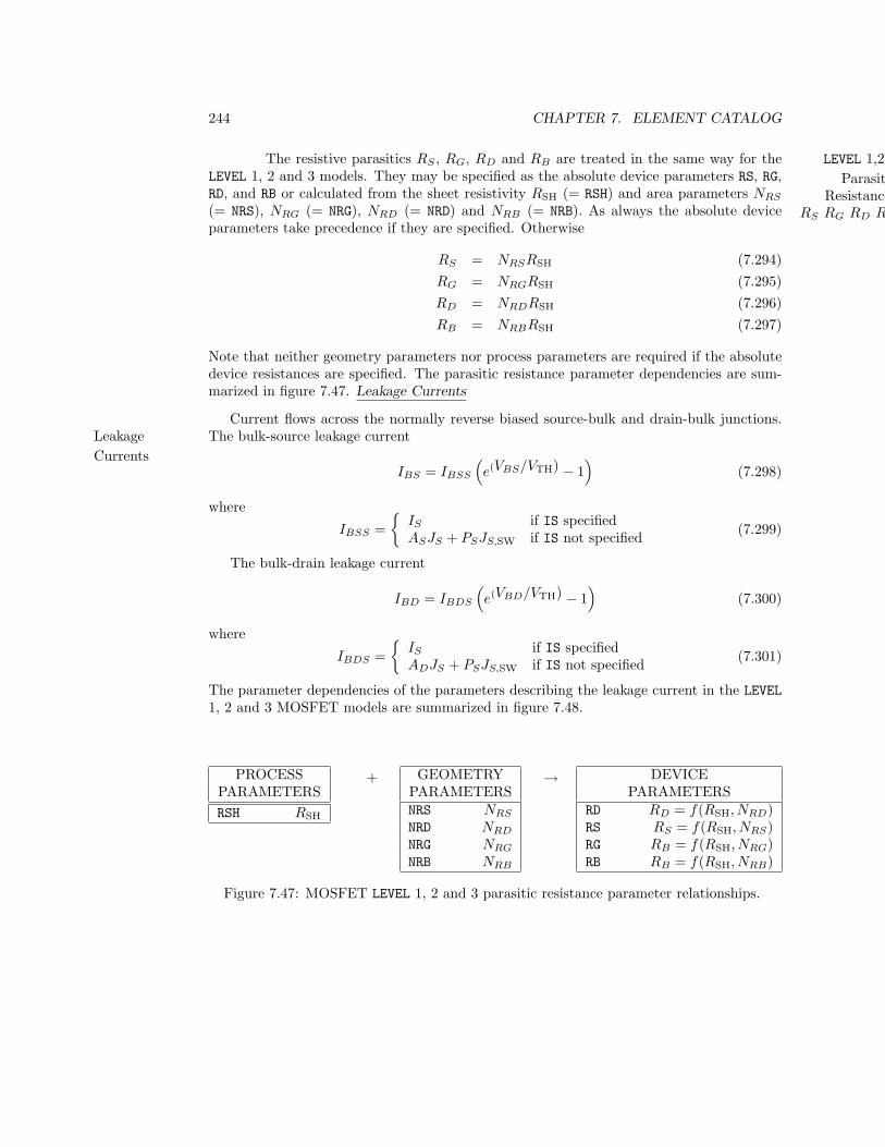
244 CHAPTER 7. ELEMENT CATALOG
The resistive parasitics RS , RG, RD and RB are treated in the same way for the LEVEL 1,2 3Parasitic
ResistancesRS RG RD RB
LEVEL 1, 2 and 3 models. They may be specified as the absolute device parameters RS, RG,RD, and RB or calculated from the sheet resistivity RSH (= RSH) and area parameters NRS
(= NRS), NRG (= NRG), NRD (= NRD) and NRB (= NRB). As always the absolute deviceparameters take precedence if they are specified. Otherwise
RS = NRSRSH (7.294)RG = NRGRSH (7.295)RD = NRDRSH (7.296)RB = NRBRSH (7.297)
Note that neither geometry parameters nor process parameters are required if the absolutedevice resistances are specified. The parasitic resistance parameter dependencies are sum-marized in figure 7.47. Leakage Currents
Current flows across the normally reverse biased source-bulk and drain-bulk junctions.LeakageCurrents
The bulk-source leakage current
IBS = IBSS
(e(VBS/VTH) − 1
)(7.298)
where
IBSS =
IS if IS specifiedASJS + PSJS,SW if IS not specified (7.299)
The bulk-drain leakage current
IBD = IBDS
(e(VBD/VTH) − 1
)(7.300)
where
IBDS =
IS if IS specifiedADJS + PSJS,SW if IS not specified (7.301)
The parameter dependencies of the parameters describing the leakage current in the LEVEL1, 2 and 3 MOSFET models are summarized in figure 7.48.
PROCESSPARAMETERSRSH RSH
+ GEOMETRYPARAMETERSNRS NRS
NRD NRD
NRG NRG
NRB NRB
→ DEVICEPARAMETERS
RD RD = f(RSH, NRD)RS RS = f(RSH, NRS)RG RB = f(RSH, NRG)RB RB = f(RSH, NRB)
Figure 7.47: MOSFET LEVEL 1, 2 and 3 parasitic resistance parameter relationships.
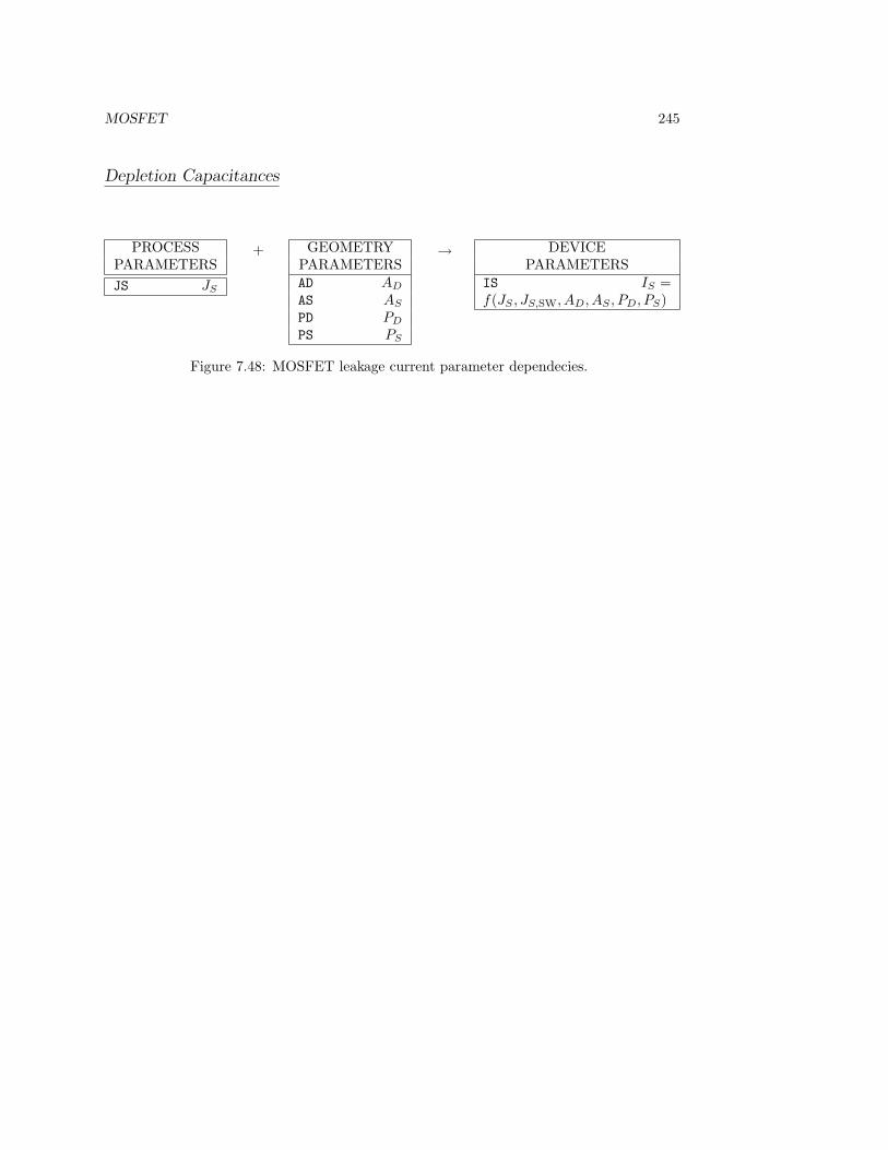
MOSFET 245
Depletion Capacitances
PROCESSPARAMETERSJS JS
+ GEOMETRYPARAMETERSAD AD
AS AS
PD PD
PS PS
→ DEVICEPARAMETERS
IS IS =f(JS , JS,SW, AD, AS , PD, PS)
Figure 7.48: MOSFET leakage current parameter dependecies.
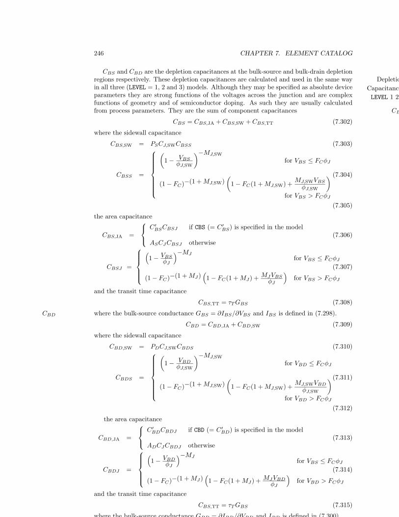
246 CHAPTER 7. ELEMENT CATALOG
CBS and CBD are the depletion capacitances at the bulk-source and bulk-drain depletionDepletion
CapacitancesLEVEL 1 2 3
regions respectively. These depletion capacitances are calculated and used in the same wayin all three (LEVEL = 1, 2 and 3) models. Although they may be specified as absolute deviceparameters they are strong functions of the voltages across the junction and are complexfunctions of geometry and of semiconductor doping. As such they are usually calculatedfrom process parameters. They are the sum of component capacitances CBS
CBS = CBS,JA + CBS,SW + CBS,TT (7.302)
where the sidewall capacitance
CBS,SW = PSCJ,SWCBSS (7.303)
CBSS =
(1− VBS
φJ,SW
)−MJ,SW
for VBS ≤ FCφJ
(1− FC)−(1 + MJ,SW)(
1− FC(1 + MJ,SW) + MJ,SWVBS
φJ,SW
)
for VBS > FCφJ
(7.304)
(7.305)
the area capacitance
CBS,JA =
C ′BSCBSJ if CBS (= C ′BS) is specified in the model
ASCJCBSJ otherwise(7.306)
CBSJ =
(1− VBS
φJ
)−MJfor VBS ≤ FCφJ
(1− FC)−(1 + MJ )(1− FC(1 + MJ) + MJVBS
φJ
)for VBS > FCφJ
(7.307)
and the transit time capacitance
CBS,TT = τT GBS (7.308)
where the bulk-source conductance GBS = ∂IBS/∂VBS and IBS is defined in (7.298).CBD
CBD = CBD,JA + CBD,SW (7.309)
where the sidewall capacitance
CBD,SW = PDCJ,SWCBDS (7.310)
CBDS =
(1− VBD
φJ,SW
)−MJ,SW
for VBD ≤ FCφJ
(1− FC)−(1 + MJ,SW)(
1− FC(1 + MJ,SW) + MJ,SWVBD
φJ,SW
)
for VBD > FCφJ
(7.311)
(7.312)
the area capacitance
CBD,JA =
C ′BDCBDJ if CBD (= C ′BD) is specified in the model
ADCJCBDJ otherwise(7.313)
CBDJ =
(1− VBD
φJ
)−MJfor VBS ≤ FCφJ
(1− FC)−(1 + MJ)(1− FC(1 + MJ) + MJVBD
φJ
)for VBD > FCφJ
(7.314)
and the transit time capacitance
CBS,TT = τT GBS (7.315)
where the bulk-source conductance GBD = ∂IBD/∂VBD and IBD is defined in (7.300).

MOSFET 247
In the LEVEL 1 MOSFET model the depletion capacitances are piecewise linear. Theyare calculated at the current operating point and then treated as linear. In the LEVEL 2 and3 models they are treated as nonlinear. The depletion capacitance parameter dependenciesare summarized in figure 7.49.
LEVEL 1 I/V Characteristics
LEVEL 1 I/VFor the LEVEL 1 model the device parameters (other than capacitances and resistances)
are evaluated using TOX (TOX), µ0 (UO), NSS (NSS and NB (NSUB) if they are not specifiedin the .MODEL statement.
The LEVEL 1 current/voltage characteristics are evaluated after first determining themode (normal: VDS ≥ 0 or inverted: VDS < 0) and the region (cutoff, linear or saturation)of the current (VDS , VGS) operating point.
Normal Mode: (VDS ≥ 0)
The regions are as follows:
cutoff region: VGS < VT
linear region: VGS > VT and VDS < VGS − VT
saturation region: VGS > VT and VDS > VGS − VT
PROCESSPARAMETERSCJ CJ
CJSW CJ,SW
MJ MJ
MJSW MJ,SW
PB φJ
PBSW φJ,SW
FC FC
+ GEOMETRYPARAMETERSAD AD
AS AS
PD PD
PS PS
→ DEVICEPARAMETERS
CBD C ′BD = f(CJ , AD)CBS C ′BS = f(CJ , AS)CBS = f(PS , C ′BS , CJ,SW, τT
MJ ,MJ,SW, φJ , φJ,SW, FC)CBD =f(PD, C ′BD, CJ,SW, τT
MJ ,MJ,SW, φJ , φJ,SW, FC)
Figure 7.49: MOSFET LEVEL 1, 2 and 3 junction depletion capacitance parameter relation-ships.
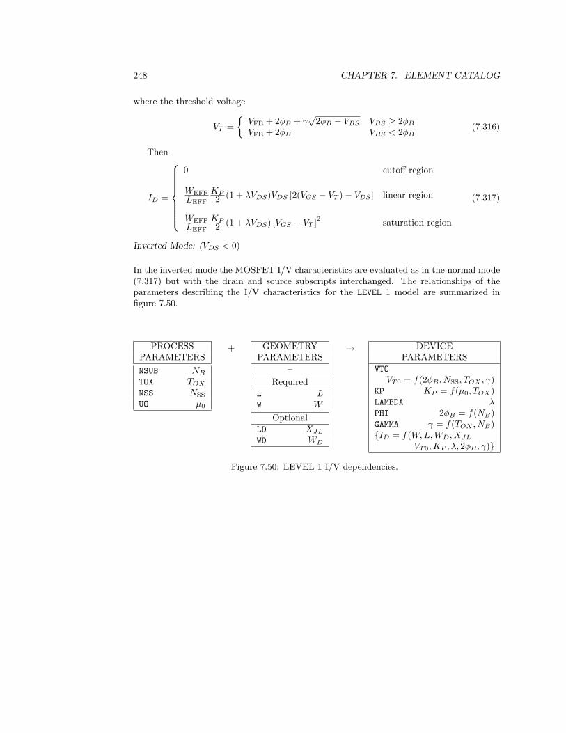
248 CHAPTER 7. ELEMENT CATALOG
where the threshold voltage
VT =
VFB + 2φB + γ√
2φB − VBS VBS ≥ 2φB
VFB + 2φB VBS < 2φB(7.316)
Then
ID =
0 cutoff region
WEFFLEFF
KP2 (1 + λVDS)VDS [2(VGS − VT )− VDS ] linear region
WEFFLEFF
KP2 (1 + λVDS) [VGS − VT ]2 saturation region
(7.317)
Inverted Mode: (VDS < 0)
In the inverted mode the MOSFET I/V characteristics are evaluated as in the normal mode(7.317) but with the drain and source subscripts interchanged. The relationships of theparameters describing the I/V characteristics for the LEVEL 1 model are summarized infigure 7.50.
PROCESSPARAMETERSNSUB NB
TOX TOX
NSS NSS
UO µ0
+ GEOMETRYPARAMETERS
–Required
L LW W
OptionalLD XJL
WD WD
→ DEVICEPARAMETERS
VTOVT0 = f(2φB , NSS, TOX , γ)
KP KP = f(µ0, TOX)LAMBDA λPHI 2φB = f(NB)GAMMA γ = f(TOX , NB)ID = f(W,L,WD, XJL
VT0,KP , λ, 2φB , γ)
Figure 7.50: LEVEL 1 I/V dependencies.
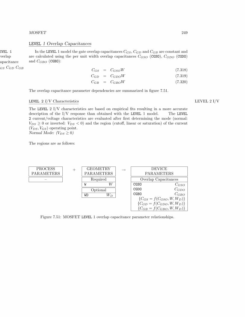
MOSFET 249
LEVEL 1 Overlap Capacitances
In the LEVEL 1 model the gate overlap capacitances CGS , CGD and CGB are constant andLEVEL 1OverlapCapacitanceCGS CGD CGB
are calculated using the per unit width overlap capacitances CGSO (CGSO), CGDO (CGDO)and CGBO (CGBO):
CGS = CGSOW (7.318)CGD = CGDOW (7.319)CGB = CGBOW (7.320)
The overlap capacitance parameter dependencies are summarized in figure 7.51.
LEVEL 2 I/V Characteristics LEVEL 2 I/V
The LEVEL 2 I/V characteristics are based on empirical fits resulting in a more accuratedescription of the I/V response than obtained with the LEVEL 1 model. The LEVEL2 current/voltage characteristics are evaluated after first determining the mode (normal:VDS ≥ 0 or inverted: VDS < 0) and the region (cutoff, linear or saturation) of the current(VDS , VGS) operating point.Normal Mode: (VDS ≥ 0)
The regions are as follows:
PROCESSPARAMETERS
–
+ GEOMETRYPARAMETERS
RequiredW W
OptionalWD WD
→ DEVICEPARAMETERS
Overlap CapacitancesCGSO CGSO
CGDO CGDO
CGBO CGBO
CGS = f(CGSO,W,WD)CGD = f(CGDO,W,WD)CGB = f(CGBO,W,WD)
Figure 7.51: MOSFET LEVEL 1 overlap capacitance parameter relationships.

250 CHAPTER 7. ELEMENT CATALOG
cutoff region: VGS < VT
weak inversion region: VT < VGS ≤ VON
linear region (strong inversion): VGS > VON and VDS < VDS,SAT
saturation region (strong inversion): VGS > VON and VDS > VDS,SAT
whereVT = V ′
FB + γEFFXS (7.321)
VON =
VT NFS = 0VT + VTHxn NFS 6= 0 (7.322)
XS =
√2φB
[1 + 12VBS/(2φB)]
VBS > 0
√2φB − VBS VBS ≤ 0
(7.323)
wherexn = 1 + FN − γEFFX1 −X2XS + WEFFLEFF
qNFS
C ′OX
(7.324)
η = 1 + FN (7.325)the effect of channel width on threshold voltage is modeled by
V ′FB = VFB + FN (2φB − VBS) (7.326)
and the flat band voltage, VFB, is calculated using (7.272) or (7.273).
VGST = VGS − VON (7.327)
The factor describing the effect of channel width on threshold is
FN =εsδπ
4C ′OXWEFF(7.328)
The effective bulk threshold parameter is affected by charge in the drain and source depletionregions. This is important for short channels. The factor describing short channel effects is
γEFF =
γ γ ≤ 0 or NB ≤ 0γ(1− FDD − FSD) γ > 0 and NB > 0 (7.329)
where the effect of depletion charge at the drain is described by
FDD =
12
(√1 + 2XDXB − 1
)VDS ≤ VDS,SAT
12
(√1 + 2XDXB,SAT − 1
) XJLEFF
VDS > VDS,SAT
(7.330)
the effect of depletion charge at the source is described by
FSD =12
(√1 + 2XDXS − 1
) XJ
LEFF(7.331)
and
XB =
√2φB
[1 + 12 (VBS − VDS)/(2φB)]
VDS < VBS
√2φB + VDS − VBS VDS ≤ VBS
(7.332)
and for saturation
XB,SAT =
√2φB
[1 + 12 (VBS − VDS,SAT)/(2φB)]
VDS,SAT < VBS
√2φB + VDS,SAT − VBS VDS,SAT ≥ VBS
(7.333)
XS is evaluated using (7.323) and XD using (7.402).
X1 =
−X2S
2(2φB)(3/2) VBS > 0
− 12XS
VBS ≤ 0
(7.334)
and
X2 =
−γ 12
XDX1LEFFXS
XJ > 0
0 XJ ≤ 0(7.335)
The effective mobility due to modulation by the gate
µEFF =
µ0
(UC
VGS − VON
)UEXPCOX 6= 0 and (VGS − VON ) > UC
µ0 COX = 0 or (VGS − VON ) ≤ UC
(7.336)
and the factor describing this effect
FG =µEFF
µ0(7.337)
The channel shortening factor
FD =LEFF
L′EFF
(7.338)
where the effective channel length due to channel shortening is
L′EFF =
XWB1 + (∆L − LEFF + XWB)/XWB
(1− λVDS)LEFF < XWB
(1− λVDS)LEFF (1− λVDS)LEFF ≥ XWB
(7.339)
The expression for L′EFF when (1 − λVDS)LEFF < XWB limits chanel shortening atpunch-through. In (7.339)
∆L = λVDSLEFF (7.340)and the distance that the depletion region at the drain extends into the channel is
XWB =
XD
√φJ NB 6= 0
0.25 10−6 NB = 0 (7.341)
The pinch-off voltage
VP =
MAX((VGSX − V ′FB), 0) γEFF
η ≤ 0
VTγEFF
η > 0 and XV ≤ 0
VTγEFF
η > 0 and X3 < 0
V ′FB + ηVDS +
√X3
γEFFη > 0 and X3 ≥ 0 and XV > 0
(7.342)
where
X3 = (VDS + 2φB − VBS)(
γEFF
η
)2
(7.343)
The drain-source saturation voltage
VDS,SAT =
VP (Grove Frohman approximation) VMAX ≤ 0
VDS,SAT from Baum’s theory of VMAX > 0velocity saturation
(7.344)
In Baum’s theory of velocity saturation the saturation voltage, VDS,SAT, is the solution ofthe quartic equation
aV 4DS,SAT + bV 3
DS,SAT + cV 2DS,SAT + dVDS,SAT = 0 (7.345)
where
a =34
γEFF
η(7.346)
b = −2(V1 + VX) (7.347)
c = −2γEFF
ηVX (7.348)
d = 2V1(V2 + VX)− V 22 −
34
γEFF
ηX3
S (7.349)
V1 =(VGSX − V ′
FB)η
+ 2φB − VBS (7.350)
V2 = 2φB − VBS (7.351)
VX =VMAXLEFF
µEFF(7.352)
The body effect factor isFB = X3
B −X3S (7.353)
and the body effect factor in saturation is
FB,EFF = X3B,SAT −X3
S (7.354)
cutoff regionID = 0 (7.355)
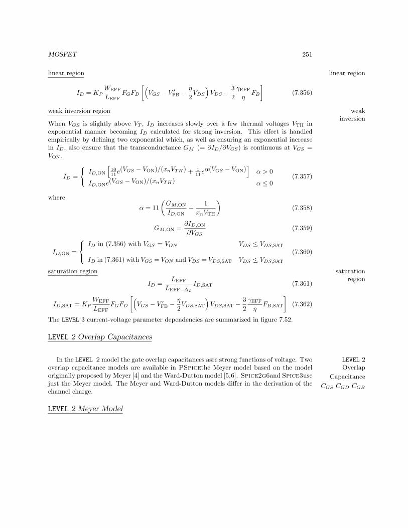
MOSFET 251
linear region linear region
ID = KPWEFF
LEFFFGFD
[(VGS − V ′
FB −η
2VDS
)VDS − 3
2γEFF
ηFB
](7.356)
weak inversion region weakinversion
When VGS is slightly above VT , ID increases slowly over a few thermal voltages VTH inexponential manner becoming ID calculated for strong inversion. This effect is handledempirically by defining two exponential which, as well as ensuring an exponential increasein ID, also ensure that the transconductance GM (= ∂ID/∂VGS) is continuous at VGS =VON.
ID =
ID,ON
[1011e(VGS − VON)/(xnVTH) + 1
11eα(VGS − VON)]
α > 0
ID,ONe(VGS − VON)/(xnVTH) α ≤ 0(7.357)
where
α = 11(
GM,ON
ID,ON− 1
xnVTH
)(7.358)
GM,ON =∂ID,ON
∂VGS(7.359)
ID,ON =
ID in (7.356) with VGS = VON VDS ≤ VDS,SAT
ID in (7.361) with VGS = VON and VDS = VDS,SAT VDS ≤ VDS,SAT
(7.360)
saturation region saturationregion
ID =LEFF
LEFF−∆L
ID,SAT (7.361)
ID,SAT = KPWEFF
LEFFFGFD
[(VGS − V ′
FB −η
2VDS,SAT
)VDS,SAT − 3
2γEFF
ηFB,SAT
](7.362)
The LEVEL 3 current-voltage parameter dependencies are summarized in figure 7.52.
LEVEL 2 Overlap Capacitances
In the LEVEL 2 model the gate overlap capacitances asre strong functions of voltage. Two LEVEL 2Overlap
CapacitanceCGS CGD CGB
overlap capacitance models are available in PSpicethe Meyer model based on the modeloriginally proposed by Meyer [4] and the Ward-Dutton model [5,6]. Spice2g6and Spice3usejust the Meyer model. The Meyer and Ward-Dutton models differ in the derivation of thechannel charge.
LEVEL 2 Meyer Model
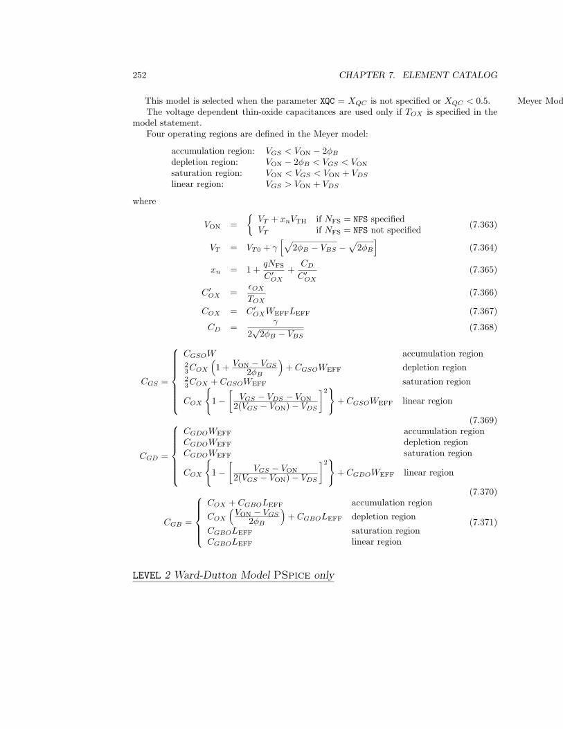
252 CHAPTER 7. ELEMENT CATALOG
This model is selected when the parameter XQC = XQC is not specified or XQC < 0.5. Meyer ModelThe voltage dependent thin-oxide capacitances are used only if TOX is specified in the
model statement.Four operating regions are defined in the Meyer model:
accumulation region: VGS < VON − 2φB
depletion region: VON − 2φB < VGS < VON
saturation region: VON < VGS < VON + VDS
linear region: VGS > VON + VDS
where
VON =
VT + xnVTH if NFS = NFS specifiedVT if NFS = NFS not specified (7.363)
VT = VT0 + γ[√
2φB − VBS −√
2φB
](7.364)
xn = 1 +qNFS
C ′OX
+CD
C ′OX
(7.365)
C ′OX =εOX
TOX(7.366)
COX = C ′OXWEFFLEFF (7.367)
CD =γ
2√
2φB − VBS(7.368)
CGS =
CGSOW accumulation region23COX
(1 + VON − VGS
2φB
)+ CGSOWEFF depletion region
23COX + CGSOWEFF saturation region
COX
1−
[VGS − VDS − VON
2(VGS − VON)− VDS
]2
+ CGSOWEFF linear region
(7.369)
CGD =
CGDOWEFF accumulation regionCGDOWEFF depletion regionCGDOWEFF saturation region
COX
1−
[VGS − VON
2(VGS − VON)− VDS
]2
+ CGDOWEFF linear region
(7.370)
CGB =
COX + CGBOLEFF accumulation regionCOX
(VON − VGS
2φB
)+ CGBOLEFF depletion region
CGBOLEFF saturation regionCGBOLEFF linear region
(7.371)
LEVEL 2 Ward-Dutton Model PSpice only
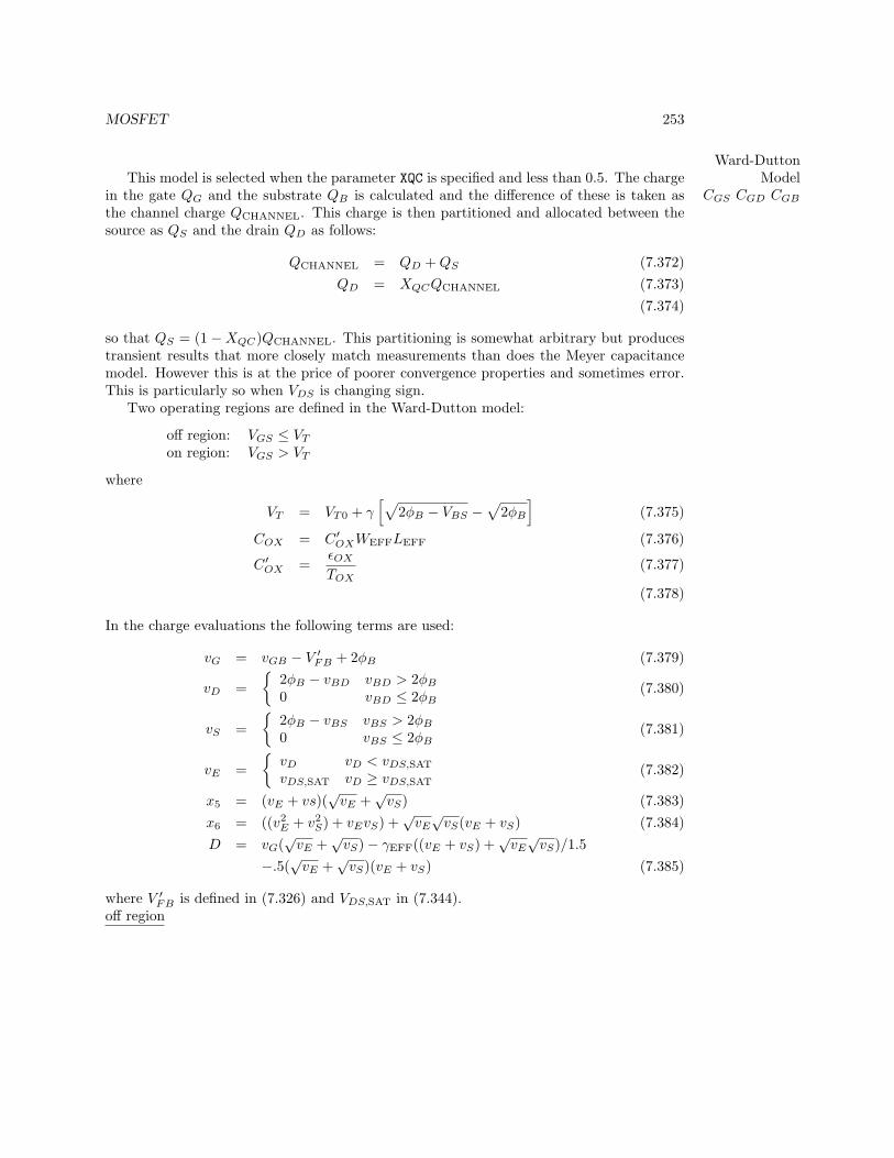
MOSFET 253
Ward-DuttonModel
CGS CGD CGB
This model is selected when the parameter XQC is specified and less than 0.5. The chargein the gate QG and the substrate QB is calculated and the difference of these is taken asthe channel charge QCHANNEL. This charge is then partitioned and allocated between thesource as QS and the drain QD as follows:
QCHANNEL = QD + QS (7.372)QD = XQCQCHANNEL (7.373)
(7.374)
so that QS = (1−XQC)QCHANNEL. This partitioning is somewhat arbitrary but producestransient results that more closely match measurements than does the Meyer capacitancemodel. However this is at the price of poorer convergence properties and sometimes error.This is particularly so when VDS is changing sign.
Two operating regions are defined in the Ward-Dutton model:
off region: VGS ≤ VT
on region: VGS > VT
where
VT = VT0 + γ[√
2φB − VBS −√
2φB
](7.375)
COX = C ′OXWEFFLEFF (7.376)
C ′OX =εOX
TOX(7.377)
(7.378)
In the charge evaluations the following terms are used:
vG = vGB − V ′FB + 2φB (7.379)
vD =
2φB − vBD vBD > 2φB
0 vBD ≤ 2φB(7.380)
vS =
2φB − vBS vBS > 2φB
0 vBS ≤ 2φB(7.381)
vE =
vD vD < vDS,SAT
vDS,SAT vD ≥ vDS,SAT(7.382)
x5 = (vE + vs)(√
vE +√
vS) (7.383)x6 = ((v2
E + v2S) + vEvS) +
√vE√
vS(vE + vS) (7.384)D = vG(
√vE +
√vS)− γEFF((vE + vS) +
√vE√
vS)/1.5−.5(
√vE +
√vS)(vE + vS) (7.385)
where V ′FB is defined in (7.326) and VDS,SAT in (7.344).
off region
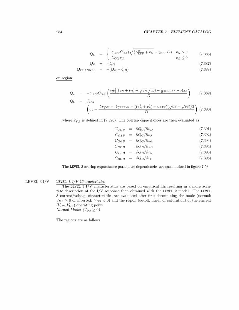
254 CHAPTER 7. ELEMENT CATALOG
QG =
γEFFCOX(
√14γ2
EFF + vG − γEFF/2) vG > 0COXvG vG ≤ 0
(7.386)
QB = −QG (7.387)QCHANNEL = −(QG + QB) (7.388)
on region
QB = −γEFFCOX
(vg 2
3 ((vE + vS) +√
vE√
vS)− 12γEFFx5 − .4x6
D
)(7.389)
QG = COX(vg − .5vgx5 − .4γEFFx6 − ((v2
E + v2S) + vEvS)(
√vE +
√vS)/3
D
)(7.390)
where V ′FB is defined in (7.326). The overlap capacitances are then evaluated as
CGDB = ∂QG/∂vD (7.391)CGSB = ∂QG/∂vS (7.392)CGGB = ∂QG/∂vG (7.393)CBDB = ∂QB/∂vD (7.394)CBSB = ∂QB/∂vS (7.395)CBGB = ∂QB/∂vG (7.396)
The LEVEL 2 overlap capacitance parameter dependencies are summarized in figure 7.53.
LEVEL 3 I/V CharacteristicsLEVEL 3 I/VThe LEVEL 3 I/V characteristics are based on empirical fits resulting in a more accu-
rate description of the I/V response than obtained with the LEVEL 2 model. The LEVEL3 current/voltage characteristics are evaluated after first determining the mode (normal:VDS ≥ 0 or inverted: VDS < 0) and the region (cutoff, linear or saturation) of the current(VDS , VGS) operating point.Normal Mode: (VDS ≥ 0)
The regions are as follows:
MOSFET 255
cutoff region: VGS < VT
weak inversion region: VT < VGS ≤ VON
linear region (strong inversion): VGS > VON and VDS < VDS,SAT
saturation region (strong inversion): VGS > VON and VDS > VDS,SAT
whereVT = VT0 − σVDS + FC (7.397)
the effect of short and narrow channel on threshold voltage
FC = γFS
√2φB − VBS + FN (2φB − VBS) (7.398)
and
VON =
VT NFS = 0VT + VTHxn NFS 6= 0 (7.399)
The effect of the short channel is described by Short ChannelEffect
FS = 1− XJ
LEFF
(XJL + WC
XJ
√1− WP
XJ + WP− XJL
XJ
)(7.400)
whereWP = XD
√φJ − VBS (7.401)
XD =√
2εs
qNB(7.402)
WC = XJ
[0.0831353 + 0.8013929
WP
XJ+ 0.0111077
WP
XJ
](7.403)
and
σ = η8.15−22
C ′OXL3EFF
(7.404)
The effect of channel width on threshold is Narrow ChannelEffect
FN =εsδπ
4C ′OXWEFF(7.405)
The effective mobility due to modulation by the gate Gate MobilityEffectµS = µ0FG (7.406)
and the factor describing mobility modulation by the gate is
FG =1
1 + θ(VGSX − VT )(7.407)
where
VGSX =
VGS VGS < VON
VON VGS ≥ VON(7.408)
The drain-source saturation voltage
VDS,SAT =
VA + VB −√
V 2A + V 2
B VMAX > 0VP VMAX ≤ 0
(7.409)
whereVA =
VGSX − VT
1 + FB(7.410)
VB =vMAXLEFF
µS(7.411)
VP = VGSX − VT (7.412)The body effect factor
FB =γFS
4√
φBS
+ FN (7.413)
where
φBS =
2φB − VBS VBS ≤ 02φB√
1 + 12VBS/(2φB)
VBS > 0 (7.414)
The velocity saturation factor is VelocitySaturation
FD =
11 + VDS/VB
forVMAX 6= 0
1 forVMAX = 0(7.415)
cutoff regionID = 0 (7.416)
256 CHAPTER 7. ELEMENT CATALOG
linear region
ID = KPWEFF
LEFFFGFD
[VGSX − VT − 1 + FB
2VDS
]VDS (7.417)
weak inversion region
When VGS is slightly above VT , ID increases slowly over a few thermal voltages VTH inexponential manner becoming ID calculated for strong inversion. This effect is handledempirically by defining two exponential which, as well as ensuring an exponential increasein ID, also ensure that the transconductance GM (= ∂ID/∂VGS) is continuous at VGS =VON.
ID =
ID,ON
[1011e(VGS − VON)/(xnVTH) + 1
11eα(VGS − VON)]
α > 0
ID,ONe(VGS − VON)/(xnVTH) α ≤ 0
(7.418)
where
α = 11(
GM,ON
ID,ON− 1
xnVTH
)(7.419)
GM,ON =∂ID,ON
∂VGS(7.420)
and
ID,ON =
ID in (7.417) with VGS = VON VDS ≤ VDS,SAT
ID in (7.422) with VGS = VON and VDS = VDS,SAT VDS ≤ VDS,SAT
(7.421)
MOSFET 257
saturation region
ID =LEFF
LEFF−∆L
ID,SAT (7.422)
ID,SAT = KPWEFF
LEFFFGFD
[VGSX − VT − 1 + FB
2VDS,SAT
]VDS,SAT (7.423)
The reduction in the channel length due to VDS modulation is
∆L =
∆′
L ∆′L < 1
2LEFF
LEFF − LEFF∆′
L∆′
L ≥ 12LEFF
(7.424)
where the punch through approximation is used for ∆′L ≥ 1
2LEFF¿ In (7.424) the distancethat the depletion region at the drain extends into the channel is
∆′L =
√(EP X2
D
2
)2
+ κX2D(VDS − VDS,SAT)− EP X2
D
2(7.425)
andEP =
ID,SAT
GDS,SATLEFF(7.426)
HereGDS,SAT =
∂ID,SAT
∂VDS,SAT(7.427)
The LEVEL 3 current-voltage parameter dependencies are summarized in figure 7.54.
LEVEL 3 Overlap Capacitances
LEVEL 3Overlap
CapacitanceCGS CGD CGB
In the LEVEL 3 model the gate overlap capacitances asre strong functions of voltage. Twooverlap capacitance models are available the Meyer model based on the model originallyproposed by Meyer [4] and the Ward-Dutton model [5, 6]. These models differ in thederivation of the channel charge.
LEVEL 3 Meyer Model
This model is selected when the parameter XQC = XQC is not specified or XQC < 0.5. Meyer ModelThe voltage dependent thin-oxide capacitances are used only if TOX is specified in the
model statement.Four operating regions are defined in the Meyer model:
accumulation region: VGS < VON − 2φB
depletion region: VON − 2φB < VGS < VON
saturation region: VON < VGS < VON + VDS
linear region: VGS > VON + VDS

258 CHAPTER 7. ELEMENT CATALOG
where
VON =
VT + xnVTH if NFS = NFS specifiedVT if NFS = NFS not specified (7.428)
VT = VT0 + γ[√
2φB − VBS −√
2φB
](7.429)
xn = 1 +qNFS
C ′OX
+CD
C ′OX
(7.430)
C ′OX =εOX
TOX(7.431)
COX = C ′OXWEFFLEFF (7.432)
CD =γ
2√
2φB − VBS(7.433)
CGS =
CGSOW accumulation region23COX
(1 + VON − VGS
2φB
)+ CGSOWEFF depletion region
23COX + CGSOWEFF saturation region
COX
1−
[VGS − VDS − VON
2(VGS − VON)− VDS
]2
+ CGSOWEFF linear region
(7.434)
CGD =
CGDOWEFF accumulation regionCGDOWEFF depletion regionCGDOWEFF saturation region
COX
1−
[VGS − VON
2(VGS − VON)− VDS
]2
+ CGDOWEFF linear region
(7.435)
CGB =
COX + CGBOLEFF accumulation regionCOX
(VON − VGS
2φB
)+ CGBOLEFF depletion region
CGBOLEFF saturation regionCGBOLEFF linear region
(7.436)
LEVEL 3 Ward-Dutton Model

MOSFET 259
Ward-DuttonModelCGS CGD CGB
This model is selected when the parameter XQC is specified and less than 0.5. The chargein the gate QG and the substrate QB is calculated and the difference of these is taken asthe channel charge QCHANNEL. This charge is then partitioned and allocated between thesource as QS and the drain QD as follows:
QCHANNEL = QD + QS (7.437)QD = XQCQCHANNEL (7.438)
(7.439)
so that QS = (1−XQC)QCHANNEL. This partitioning is somewhat arbitrary but producestransient results that more closely match measurements than does the Meyer capacitancemodel. However this is at the price of poorer convergence properties and sometimes error.This is particularly so when VDS is changing sign. Two operating regions are defined in theWard-Dutton model:
off region: VGS ≤ V ′T
on region: VGS > V ′T
where
V ′T = vBIX + FC (7.440)
vBIX = VFB − σVDS (7.441)
FC is defined in (7.398), σ in (7.404) and VFB is defined in (7.272) or (7.272). off region
QG =
γFSCOX
[√(γFS2
)2
+ (vGB − VFB + 2φB)− γFS2
]
vGB > (VFB − 2φB)
COX(vGB − VFB + 2φB) vGB ≤ (VFB − 2φB)
(7.442)
QB = −QG (7.443)
on region
260 CHAPTER 7. ELEMENT CATALOG
QG =
COX(VGS − VFB) VDSX = 0COX(VGS − vBIX − 1
2VDSX + xa) VDSX 6= 0 (7.444)
QB = −COXFC VDSX = 0−COX(FC + 1
2FBVDSX − xaFB) VDSX 6= 0 (7.445)
where
xa =(1 + FB)V 2
DSX
12VGSX − V ′T − 1
2 (1 + FB)VDSX
(7.446)
QCHANNEL = −(QG + QB) (7.447)
where FB is defined in (7.413), VGSX in (7.408) and
VDSX =
VDS,SAT VDS > VD,SAT
VDS VDS ≤ VD,SAT(7.448)
The overlap capacitances are then evaluated as
CGDB = ∂QG/∂vD (7.449)CGSB = ∂QG/∂vS (7.450)CGGB = ∂QG/∂vG (7.451)CBDB = ∂QB/∂vD (7.452)CBSB = ∂QB/∂vS (7.453)CBGB = ∂QB/∂vG (7.454)
The overlap capacitance parameter dependencies are summarized in figure 7.55.
BSIM1 (LEVEL 4) MOSFET models.
BSIMLEVEL 4
The parameters of the BSIM1 (LEVEL 4 model are all values obtained from processcharacterization, and can be generated automatically. J. Pierret [10] describes a means ofgenerating a ‘process’ file, and the program Proc2Mod provided in the UC Berkeley standardSPICE3 distribution converts this file into a sequence of .MODEL lines suitable for inclusionin a SPICE circuit file. Parameters marked below with an * in the L/W column also havecorresponding parameters with a length and width dependency.
Unlike most other models the BSIM1 model is designed for use with a process characteri-zation system that provides all the parameters, thus there are no defaults for the parameters,and leaving one out is considered an error.Table 7.9 continued: BSIM (LEVEL) 4 model keywords.
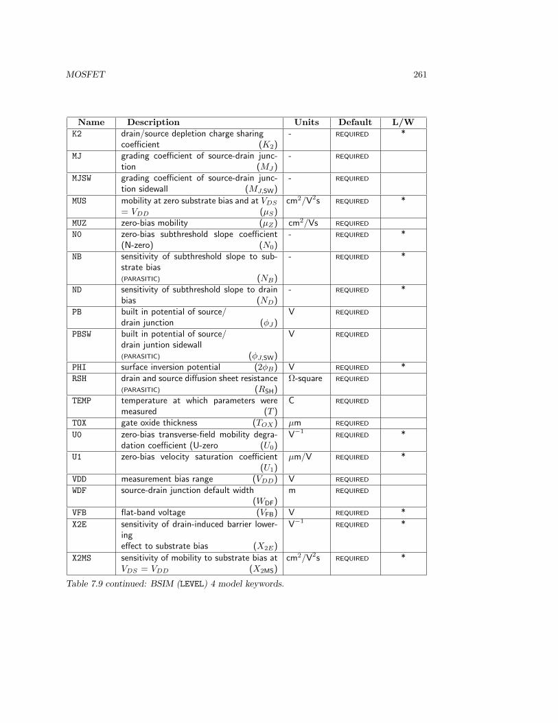
MOSFET 261
Name Description Units Default L/WK2 drain/source depletion charge sharing
coefficient (K2)- REQUIRED *
MJ grading coefficient of source-drain junc-tion (MJ )
- REQUIRED
MJSW grading coefficient of source-drain junc-tion sidewall (MJ,SW)
- REQUIRED
MUS mobility at zero substrate bias and at VDS
= VDD (µS)cm2/V2s REQUIRED *
MUZ zero-bias mobility (µZ) cm2/Vs REQUIRED
N0 zero-bias subthreshold slope coefficient(N-zero) (N0)
- REQUIRED *
NB sensitivity of subthreshold slope to sub-strate bias(PARASITIC) (NB)
- REQUIRED *
ND sensitivity of subthreshold slope to drainbias (ND)
- REQUIRED *
PB built in potential of source/drain junction (φJ )
V REQUIRED
PBSW built in potential of source/drain juntion sidewall(PARASITIC) (φJ,SW)
V REQUIRED
PHI surface inversion potential (2φB) V REQUIRED *RSH drain and source diffusion sheet resistance
(PARASITIC) (RSH)Ω-square REQUIRED
TEMP temperature at which parameters weremeasured (T )
C REQUIRED
TOX gate oxide thickness (TOX) µm REQUIRED
U0 zero-bias transverse-field mobility degra-dation coefficient (U-zero (U0)
V−1REQUIRED *
U1 zero-bias velocity saturation coefficient(U1)
µm/V REQUIRED *
VDD measurement bias range (VDD) V REQUIRED
WDF source-drain junction default width(WDF)
m REQUIRED
VFB flat-band voltage (VFB) V REQUIRED *
X2E sensitivity of drain-induced barrier lower-ingeffect to substrate bias (X2E)
V−1REQUIRED *
X2MS sensitivity of mobility to substrate bias atVDS = VDD (X2MS)
cm2/V2s REQUIRED *
Table 7.9 continued: BSIM (LEVEL) 4 model keywords.
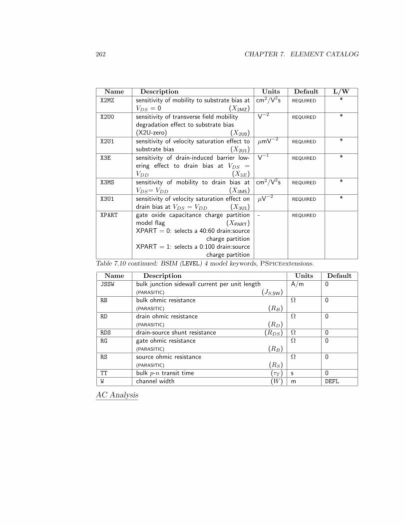
262 CHAPTER 7. ELEMENT CATALOG
Name Description Units Default L/WX2MZ sensitivity of mobility to substrate bias at
VDS = 0 (X2MZ)cm2/V2s REQUIRED *
X2U0 sensitivity of transverse field mobilitydegradation effect to substrate bias(X2U-zero) (X2U0)
V−2REQUIRED *
X2U1 sensitivity of velocity saturation effect tosubstrate bias (X2U1)
µmV−2REQUIRED *
X3E sensitivity of drain-induced barrier low-ering effect to drain bias at VDS =VDD (X3E)
V−1REQUIRED *
X3MS sensitivity of mobility to drain bias atVDS= VDD (X3MS)
cm2/V2s REQUIRED *
X3U1 sensitivity of velocity saturation effect ondrain bias at VDS = VDD (X3U1)
µV−2REQUIRED *
XPART gate oxide capacitance charge partitionmodel flag (XPART)XPART = 0: selects a 40:60 drain:source
charge partitionXPART = 1: selects a 0:100 drain:source
charge partition
- REQUIRED
Table 7.10 continued: BSIM (LEVEL) 4 model keywords, PSpiceextensions.
Name Description Units DefaultJSSW bulk junction sidewall current per unit length
(PARASITIC) (JS,SW)A/m 0
RB bulk ohmic resistance(PARASITIC) (RB)
Ω 0
RD drain ohmic resistance(PARASITIC) (RD)
Ω 0
RDS drain-source shunt resistance (RDS) Ω 0RG gate ohmic resistance
(PARASITIC) (RB)Ω 0
RS source ohmic resistance(PARASITIC) (RS)
Ω 0
TT bulk p-n transit time (τT ) s 0W channel width (W ) m DEFL
AC Analysis
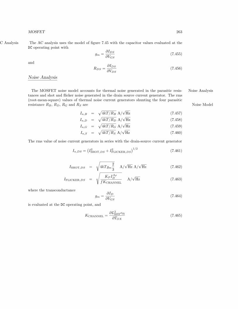
MOSFET 263
The AC analysis uses the model of figure 7.45 with the capacitor values evaluated at theAC AnalysisDC operating point with
gm =∂IDS
∂VGS(7.455)
andRDS =
∂IDS
∂VDS(7.456)
Noise Analysis
The MOSFET noise model accounts for thermal noise generated in the parasitic resis- Noise Analysistances and shot and flicker noise generated in the drain source current generator. The rms(root-mean-square) values of thermal noise current generators shunting the four parasiticresistance RB , RD, RG and RS are Noise Model
In,B =√
4kT/RB A/√
Hz (7.457)
In,D =√
4kT/RD A/√
Hz (7.458)
In,G =√
4kT/RG A/√
Hz (7.459)
In,S =√
4kT/RS A/√
Hz (7.460)
The rms value of noise current generators in series with the drain-source current generator
In,DS =(I2SHOT,DS + I2
FLICKER,DS
)1/2(7.461)
ISHOT,DS =
√4kTgm
23
A/√
Hz A/√
Hz (7.462)
IFLICKER,DS =
√KF IAF
D
fKCHANNELA/√
Hz (7.463)
where the transconductancegm =
∂ID
∂VGS(7.464)
is evaluated at the DC operating point, and
KCHANNEL =∂L2
EFFεSi
∂TOX(7.465)
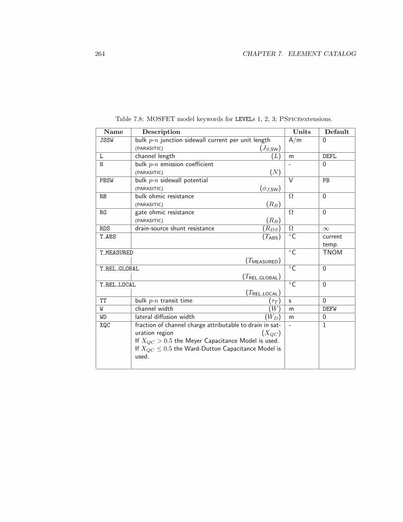
264 CHAPTER 7. ELEMENT CATALOG
Table 7.8: MOSFET model keywords for LEVELs 1, 2, 3; PSpiceextensions.
Name Description Units DefaultJSSW bulk p-n junction sidewall current per unit length
(PARASITIC) (JS,SW)A/m 0
L channel length (L) m DEFLN bulk p-n emission coefficient
(PARASITIC) (N)- 0
PBSW bulk p-n sidewall potential(PARASITIC) (φJ,SW)
V PB
RB bulk ohmic resistance(PARASITIC) (RB)
Ω 0
RG gate ohmic resistance(PARASITIC) (RB)
Ω 0
RDS drain-source shunt resistance (RDS) Ω ∞T ABS (TABS)
C currenttemp.
T MEASURED C TNOM(TMEASURED)
T REL GLOBAL C 0(TREL GLOBAL)
T REL LOCAL C 0(TREL LOCAL)
TT bulk p-n transit time (τT ) s 0W channel width (W ) m DEFWWD lateral diffusion width (WD) m 0XQC fraction of channel charge attributable to drain in sat-
uration region (XQC)If XQC > 0.5 the Meyer Capacitance Model is used.If XQC ≤ 0.5 the Ward-Dutton Capacitance Model isused.
- 1
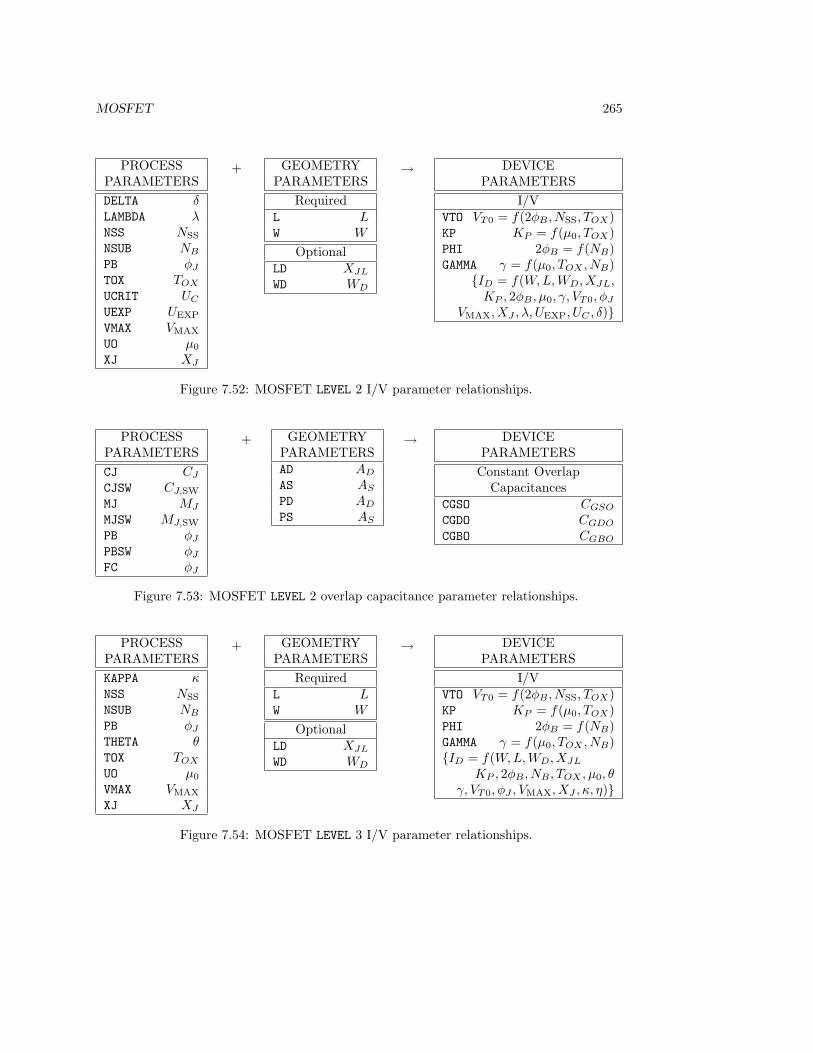
MOSFET 265
PROCESSPARAMETERSDELTA δLAMBDA λNSS NSS
NSUB NB
PB φJ
TOX TOX
UCRIT UC
UEXP UEXP
VMAX VMAX
UO µ0
XJ XJ
+ GEOMETRYPARAMETERS
RequiredL LW W
OptionalLD XJL
WD WD
→ DEVICEPARAMETERS
I/VVTO VT0 = f(2φB , NSS, TOX)KP KP = f(µ0, TOX)PHI 2φB = f(NB)GAMMA γ = f(µ0, TOX , NB)
ID = f(W,L, WD, XJL,KP , 2φB , µ0, γ, VT0, φJ
VMAX, XJ , λ, UEXP, UC , δ)
Figure 7.52: MOSFET LEVEL 2 I/V parameter relationships.
PROCESSPARAMETERSCJ CJ
CJSW CJ,SW
MJ MJ
MJSW MJ,SW
PB φJ
PBSW φJ
FC φJ
+ GEOMETRYPARAMETERSAD AD
AS AS
PD AD
PS AS
→ DEVICEPARAMETERSConstant Overlap
CapacitancesCGSO CGSO
CGDO CGDO
CGBO CGBO
Figure 7.53: MOSFET LEVEL 2 overlap capacitance parameter relationships.
PROCESSPARAMETERSKAPPA κNSS NSS
NSUB NB
PB φJ
THETA θTOX TOX
UO µ0
VMAX VMAX
XJ XJ
+ GEOMETRYPARAMETERS
RequiredL LW W
OptionalLD XJL
WD WD
→ DEVICEPARAMETERS
I/VVTO VT0 = f(2φB , NSS, TOX)KP KP = f(µ0, TOX)PHI 2φB = f(NB)GAMMA γ = f(µ0, TOX , NB)ID = f(W,L,WD, XJL
KP , 2φB , NB , TOX , µ0, θγ, VT0, φJ , VMAX, XJ , κ, η)
Figure 7.54: MOSFET LEVEL 3 I/V parameter relationships.
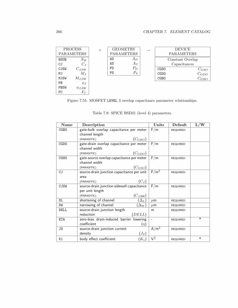
266 CHAPTER 7. ELEMENT CATALOG
PROCESSPARAMETERSNSUB NB
CJ CJ
CJSW CJ,SW
MJ MJ
MJSW MJ,SW
PB φJ
PBSW φJ,SW
FC FC
+ GEOMETRYPARAMETERSAD AD
AS AS
PD PD
PS PS
→ DEVICEPARAMETERSConstant Overlap
CapacitancesCGSO CGSO
CGDO CGDO
CGBO CGBO
Figure 7.55: MOSFET LEVEL 3 overlap capacitance parameter relationships.
Table 7.9: SPICE BSIM1 (level 4) parameters.
Name Description Units Default L/WCGBO gate-bulk overlap capacitance per meter
channel length(PARASITIC) (CGBO)
F/m REQUIRED
CGDO gate-drain overlap capacitance per meterchannel width(PARASITIC) (CGDO)
F/m REQUIRED
CGSO gate-source overlap capacitance per meterchannel width(PARASITIC) (CGSO)
F/m REQUIRED
CJ source-drain junction capacitance per unitarea(PARASITIC) (CJ )
F/m2REQUIRED
CJSW source-drain junction sidewall capacitanceper unit length(PARASITIC) (CJ,SW)
F/m REQUIRED
DL shortening of channel (∆L) µm REQUIRED
DW narrowing of channel (∆W ) µm REQUIRED
DELL source-drain junction lengthreduction (DELL)
m REQUIRED
ETA zero-bias drain-induced barrier loweringcoefficient (η)
- REQUIRED *
JS source-drain junction currentdensity (JS)
A/m2REQUIRED
K1 body effect coefficient (K1) V12 REQUIRED *
MOSFET 267
Table 7.10: SPICE BSIM1 (level 4) parameters, PSpiceextensions.
Name Description Units DefaultAF flicker noise exponent (AF ) - 1CBD zero-bias B-D junction capacitance (C ′BD) F 0CBS zero-bias B-S junction capacitance (C ′BS) F 0FC coefficient for forward-bias depletion capacitance
formula (FC)- 0.5
IS bulk junction saturation current (IS) A 1E-14KF flicker noise coefficient (KF ) - 0L channel length (L) m DEFLN bulk p-n emission coefficient
(PARASITIC) (N)- 0
PBSW bulk p-n sidewall potential(PARASITIC) (φJ,SW)
V PB
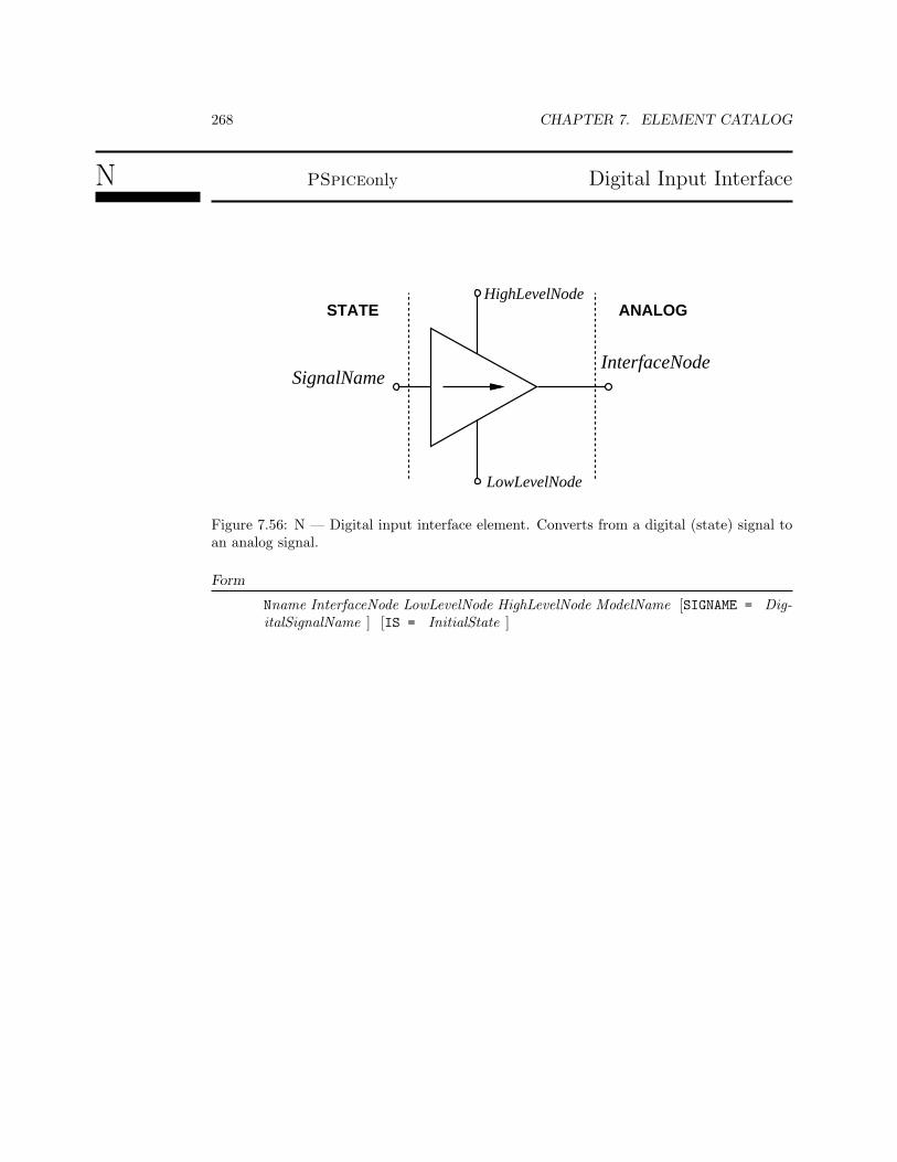
268 CHAPTER 7. ELEMENT CATALOG
N PSpiceonly Digital Input Interface
SignalNameInterfaceNode
HighLevelNode
LowLevelNode
STATE ANALOG
Figure 7.56: N — Digital input interface element. Converts from a digital (state) signal toan analog signal.
Form
Nname InterfaceNode LowLevelNode HighLevelNode ModelName [SIGNAME = Dig-italSignalName ] [IS = InitialState ]
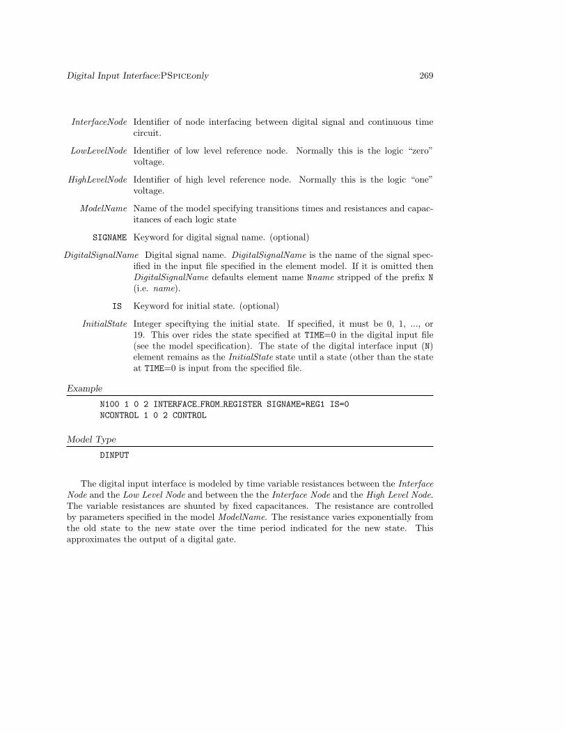
Digital Input Interface:PSpiceonly 269
InterfaceNode Identifier of node interfacing between digital signal and continuous timecircuit.
LowLevelNode Identifier of low level reference node. Normally this is the logic “zero”voltage.
HighLevelNode Identifier of high level reference node. Normally this is the logic “one”voltage.
ModelName Name of the model specifying transitions times and resistances and capac-itances of each logic state
SIGNAME Keyword for digital signal name. (optional)
DigitalSignalName Digital signal name. DigitalSignalName is the name of the signal spec-ified in the input file specified in the element model. If it is omitted thenDigitalSignalName defaults element name Nname stripped of the prefix N(i.e. name).
IS Keyword for initial state. (optional)
InitialState Integer speciftying the initial state. If specified, it must be 0, 1, ..., or19. This over rides the state specified at TIME=0 in the digital input file(see the model specification). The state of the digital interface input (N)element remains as the InitialState state until a state (other than the stateat TIME=0 is input from the specified file.
Example
N100 1 0 2 INTERFACE FROM REGISTER SIGNAME=REG1 IS=0NCONTROL 1 0 2 CONTROL
Model Type
DINPUT
The digital input interface is modeled by time variable resistances between the InterfaceNode and the Low Level Node and between the the Interface Node and the High Level Node.The variable resistances are shunted by fixed capacitances. The resistance are controlledby parameters specified in the model ModelName. The resistance varies exponentially fromthe old state to the new state over the time period indicated for the new state. Thisapproximates the output of a digital gate.
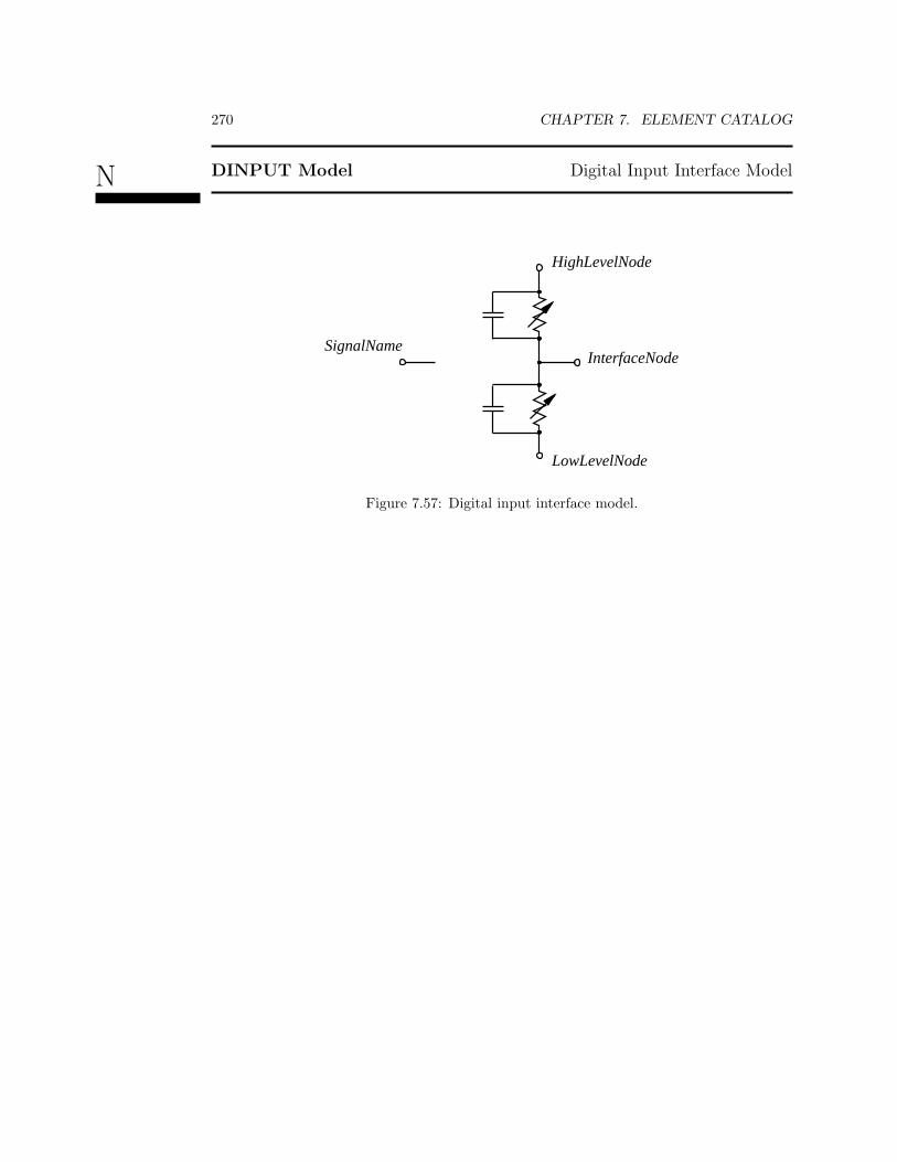
270 CHAPTER 7. ELEMENT CATALOG
N DINPUT Model Digital Input Interface Model
LowLevelNode
HighLevelNode
InterfaceNodeSignalName
Figure 7.57: Digital input interface model.
Digital Input Interface:PSpiceonly 271
Keywords:Name Description Units DefaultFILE digital input filename. If more than one model refers
to the same file then the filenames specified must beidentical and not logicly equivalent. This ensures thatthe file is opened only once.
- REQUIRED
FORMAT digital input file format - 1TIMESTEP digital input file time step s 1NSCLO capacitance to low level node F 0CHI capacitance to high level node F 0SnNAME state “n” character abreviation
n = 0, 2, ..., or 19- REQUIRED
SnTSW state “n” switching timen = 0, 2, ..., or 19
s REQUIRED
SnRLO state “n” resistance to low level noden = 0, 2, ..., or 19
Ω REQUIRED
SnRHI state “n” resistance to high level noden = 0, 2, ..., or 19
Ω REQUIRED
The digital input interface is modeled by time variable resistances between the InterfaceNode and the Low Level Node and between the the Interface Node and the High Level Node.The variable resistances are shunted by fixed capacitances. The parameters are controlledby parameters specified in the model. Upon a state transition the two resistances varyexponentially from the old state to the new state over the time period indicated for thenew state. This approximates the output of a digital gate. The sequence of states and thestate change times are specified in the file specified by the FILE = (InputFileName) keywordin the model. The initial state at TIME 0 is taken from this file unless the IS keyword isspecified on the element line. In the IS (= InitialState) keyword is specified then the stateof the digital input interface is InitialState until a state transition at TIME > 0 is specifiedin the file InputFileName.
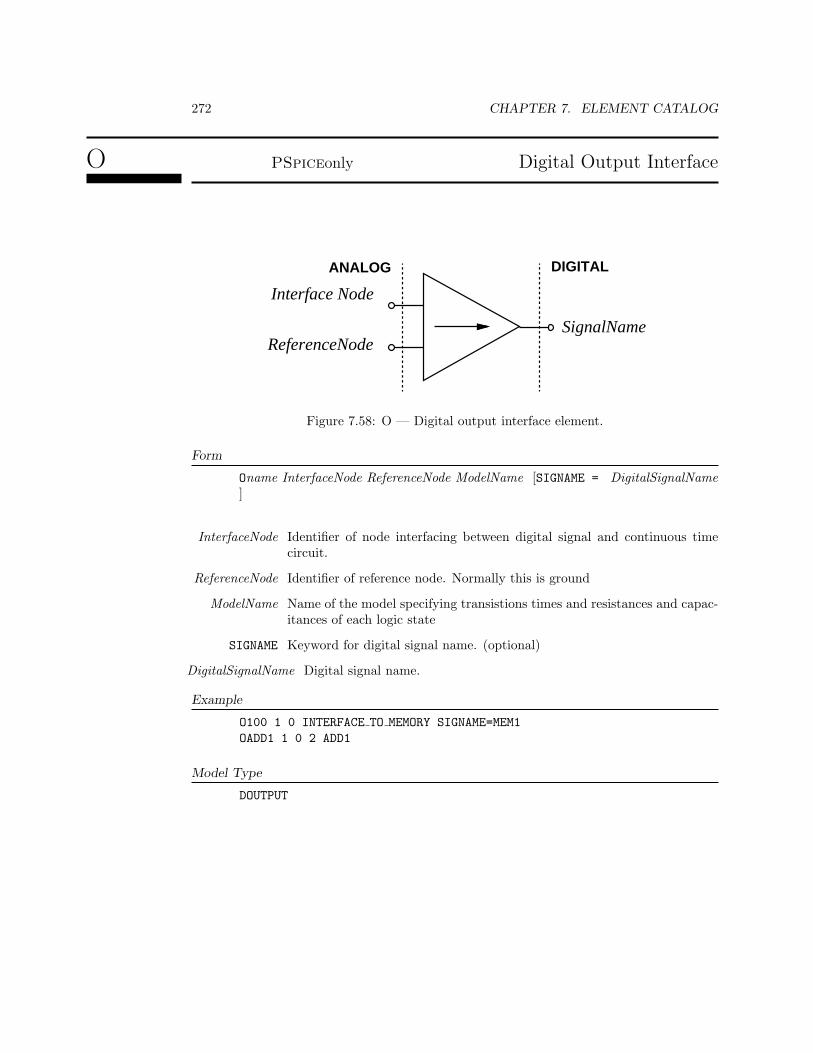
272 CHAPTER 7. ELEMENT CATALOG
O PSpiceonly Digital Output Interface
SignalName
Interface Node
ANALOG DIGITAL
ReferenceNode
Figure 7.58: O — Digital output interface element.
Form
Oname InterfaceNode ReferenceNode ModelName [SIGNAME = DigitalSignalName]
InterfaceNode Identifier of node interfacing between digital signal and continuous timecircuit.
ReferenceNode Identifier of reference node. Normally this is ground
ModelName Name of the model specifying transistions times and resistances and capac-itances of each logic state
SIGNAME Keyword for digital signal name. (optional)
DigitalSignalName Digital signal name.
Example
O100 1 0 INTERFACE TO MEMORY SIGNAME=MEM1OADD1 1 0 2 ADD1
Model Type
DOUTPUT
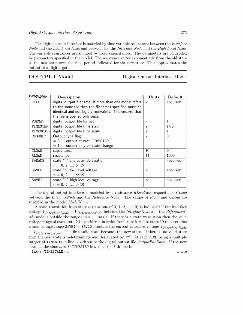
Digital Output Interface:PSpiceonly 273
The digital output interface is modeled by time variable resistances between the InterfaceNode and the Low Level Node and between the the Interface Node and the High Level Node.The variable resistances are shunted by fixed capacitances. The parameters are controlledby parameters specified in the model. The resistance varies exponentially from the old stateto the new state over the time period indicated for the new state. This approximates theoutput of a digital gate.
DOUTPUT Model Digital Output Interface Model
Keywords:Name Description Units DefaultFILE digital output filename. If more than one model refers
to the same file then the filenames specified must beidentical and not logicly equivalent. This ensures thatthe file is opened only once.
- REQUIRED
FORMAT digital output file format - 1TIMESTEP digital output file time step s 1NSTIMESCALE digital output file time scale s 1CHGONLY Output type flag:
= 0 → output at each TIMESTEP= 1 → output only on state change
- 0
CLOAD capacitance F 0RLOAD resistance Ω 1000SnNAME state “n” character abreviation
n = 0, 2, ..., or 19- REQUIRED
SnVLO state “n” low level voltagen = 0, 2, ..., or 19
s REQUIRED
SnVHI state “n” high level voltagen = 0, 2, ..., or 19
s REQUIRED
The digital output interface is modeled by a resistance RLoad and capacitance CLoadbetween the InterfaceNode and the Reference Node . The values of Rload and CLoad arespecified in the model ModelName.
A state transistion from state n (n = one of 0, 1, 2, ... 19) is indicated if the interfacevoltage VInterfaceNode − VReferenceNode between the InterfaceNode and the ReferenceN-ode node is outside the range SnVHI − SnVLO. If there is a state transistion then the validvoltage range of each state k is considered in order from state k = 0 to state 19 to determinewhich voltage range SkVHI − SkVLO brackets the current interface voltage VInterfaceNode− VReferenceNode. The first valid state becomes the new state. If there is no valid statethen the new state is indeterminate and designated by “?”. At each TIME being a multipleinteger of TIMESTEP a line is written to the digital output file OutputFileName. If the newstate at the time ti = i · TIMESTEP is n then the i th line is:int(i · TIMESCALE) n where

274 CHAPTER 7. ELEMENT CATALOG
int() is the integer operation. An example of the first few lines of OutputFileName with aTIMESTEP of 1 ns and TIMESCALE of 2 is:
0.0 12 04 26 38 ?10 112 014 1
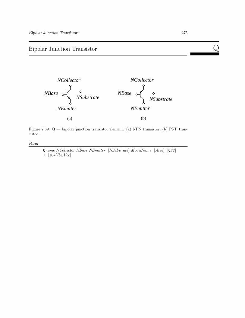
Bipolar Junction Transistor 275
Bipolar Junction Transistor Q
(a) (b)
NCollector
NEmitter
NBaseNSubstrate
NBase
NCollector
NEmitter
NSubstrate
Figure 7.59: Q — bipolar junction transistor element: (a) NPN transistor; (b) PNP tran-sistor.
Form
Qname NCollector NBase NEmitter [NSubstrate] ModelName [Area] [OFF]+ [IC=Vbe,Vce]

276 CHAPTER 7. ELEMENT CATALOG
NCollector is the collector node.
NBase is the base node.
NEmitter is the emitter node.
NSubstrate is the optional substrate node. If not specified, ground is used as thesubstrate node. If NSubstrate is a name as allowed in PSpice) it mustbe enclosed in square brackets, e.g. [NSubstrate], to distinguish it fromModelName.
ModelName is the model name.
Area is the area factorIf the area factor is omitted, a value of 1.0 is assumed. (Units: none;Optional; Default: 1; Symbol: Area)
OFF indicates an (optional) initial condition on the device for the DC analysis.If specified the DC operating point is calculated with the terminal voltagesset to zero. Once convergence is obtained, the program continues to iterateto obtain the exact value of the terminal voltages. The OFF option is usedto enforce the solution to correspond to a desired state if the circuit hasmore than one stable state.
IC is the optional initial condition specification using IC=VBE , VCE is intendedfor use with the UIC option on the .TRAN line, when a transient analysis isdesired starting from other than the quiescent operating point. See the .ICline description for a better way to set transient initial conditions.
Example
Q20 10 50 0 QFAST IC=0.65,15.0Q5PUSH 10 29 14 200 MODEL1
NPN Model NPN Si Bipolar Transistor Model
PNP Model PNP Si Bipolar Transistor Model
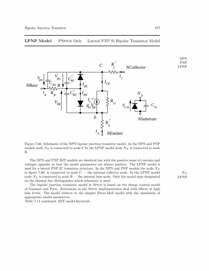
Bipolar Junction Transistor 277
LPNP Model PSpice Only Lateral PNP Si Bipolar Transistor Model
NPNPNP
LPNP
R
I
C
I
I
g Vm
I =
R
R
C
NBase
NEmitter
NCollector
VBE
BC
C O
BE
BC
BE
C
B
E
C
E
CE
R
BCV
BE
B
IE
IB
IC
CJS
NSubstrate
NX
VCJS
CBX
BXV
Figure 7.60: Schematic of the NPN bipolar junction transistor model. In the NPN and PNPmodels node NX is connected to node C In the LPNP model node NX is connected to nodeB.
The NPN and PNP BJT models are identical but with the positive sense of currents andvoltages opposite so that the model parameters are always positive. The LPNP model isused for a lateral PNP IC transistor structure. In the NPN and PNP models the node NX
in figure 7.60 is connected to node C — the internal collector node. In the LPNP model NX
node NX is connected to node B — the internal base node. Only the model type designated LPNPon the element line distinguishes which schematic is used.
The bipolar junction transistor model in Spice is based on the charge control modelof Gummel and Poon. Extensions in the Spice implementation deal with effects at highbias levels. The model reduces to the simpler Ebers-Moll model with the ommission ofappropriate model parameters.Table 7.11 continued: BJT model keywords
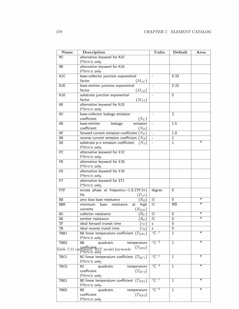
278 CHAPTER 7. ELEMENT CATALOG
Name Description Units Default AreaMC alternative keyword for MJC
PSpice only.ME alternative keyword for MJE
PSpice only.MJC base-collector junction exponential
factor (MJC)- 0.33
MJE base-emitter junction exponentialfactor (MJE)
- 0.33
MJS substrate junction exponentialfactor (MJS)
- 0
MS alternative keyword for MJSPSpice only.
NC base-collector leakage emissioncoefficient (NC)
- 2
NE base-emitter leakage emissioncoefficient (NE)
- 1.5
NF forward current emission coefficient (NF ) - 1.0NR reverse current emission coefficient (NR) - 1NS substrate p-n emission coefficient (NS)
PSpice only.- 1 *
PC alternative keyword for VJCPSpice only.
PE alternative keyword for VJEPSpice only.
PS alternative keyword for VJSPSpice only.
PT alternative keyword for XTIPSpice only.
PTF excess phase at frequency=1.0/(TF 2π)Hz (PτF )
degree 0
RB zero bias base resistance (RB) Ω 0 *RBM minimum base resistance at high
currents (RBM )Ω RB *
RC collector resistance (RC) Ω 0 *RE emitter resistance (RE) Ω 0 *TF ideal forward transit time (τF ) s 0TR ideal reverse trarsit time (τR) s 0TRB1 RB linear temperature coefficient (TRB1)
PSpice only.
C−1 1 *
TRB2 RB quadratic temperaturecoefficient (TRB2)PSpice only.
C−2 1 *
TRC1 RC linear temperature coefficient (TRC1)PSpice only.
C−1 1 *
TRC2 RC quadratic temperaturecoefficient (TRC2)PSpice only.
C−2 1 *
TRE1 RE linear temperature coefficient (TRE1)PSpice only.
C−1 1 *
TRE2 RE quadratic temperaturecoefficient (TRE2)PSpice only.
C−2 1 *
Table 7.11 continued: BJT model keywords

Bipolar Junction Transistor 279
Name Description Units Default AreaTRM1 RBM linear temperature
coefficient (TRM1)PSpice only.
C−1 1 *
TRM2 RBM quadratic temperaturecoefficient (TRM2)PSpice only.
C−2 1 *
VA alternative keyword for VAFPSpice only.
VB alternative keyword for VARPSpice only.
VAF forward Early voltage (VAF ) V ∞VAR reverse Early voltage (VAR) V ∞VJC base-collector built-in potential (VJC) V 0.75VJE base-emitter built-in potential (VJE) V 0.75VJS substrate junction built-in potential (VJS) VVTF voltage describing VBC dependence of
TF (VτF )V ∞
XCJC fraction of B-C depletion capacitance con-nected to internal base node (XCJC)
- 1
XTB forward and reverse beta temperatureexponent (XTB)
-
XTI temperature exponent for effect onIS (XTI)
- 3
XTF coefficient for bias dependence ofTF (XτF )
-
Standard Calculations
280 CHAPTER 7. ELEMENT CATALOG
The physical constants used in the model evaluation are
k Boltzman’s constant 1.3806226 10−23 J/Kq electronic charge 1.6021918 10−19 C
Absolute temperatures (in kelvins, K) are used. The thermal voltage
VTH(TNOM) =kTNOM
q. (7.466)
Temperature DependenceTemperatureDependence
Temperature effects are incorporated as follows where T and TNOM are absolute tempera-tures in Kelvins (K).
VTH =kT
q(7.467)
IS(T ) = ISe
(Eg(T ) T
TNOM− EG(T )
)/VTH +
(T
TNOM
)XT I/NF
(7.468)
ISE(T ) = ISEe
(Eg(T ) T
TNOM− EG(T )
)/VTH +
(T
TNOM
)XT I/NE
(7.469)
ISC(T ) = ISCe
(Eg(T ) T
TNOM− EG(T )
)/VTH +
(T
TNOM
)XT I/NC
(7.470)
ISS(T ) = ISSe
(Eg(T ) T
TNOM− EG(T )
)/VTH +
(T
TNOM
)XT I/NS
(7.471)
VJE(T ) = VJE(TNOM)(T − TNOM)− 3VTHln(
T
TNOM
)EG(TNOM)
T
TNOM− EG(T ) (7.472)
VJC(T ) = VJC(TNOM)(T − TNOM)− 3VTHln(
T
TNOM
)EG(TNOM)
T
TNOM− EG(T ) (7.473)
VJS(T ) = VJS(TNOM)(T − TNOM)− 3VTHln(
T
TNOM
)EG(TNOM)
T
TNOM− EG(T ) (7.474)
CJC(T ) = CJC1 + MJC [0.0004(T − TNOM) + (1− VJC(T )/VJC(TNOM))] (7.475)CJE(T ) = CJE1 + MJE [0.0004(T − TNOM) + (1− VJE(T )/VJE(TNOM))] (7.476)CJS(T ) = CJS1 + MJS [0.0004(T − TNOM) + (1− VJS(T )/VJS(TNOM))] (7.477)βF (T ) = βF (TNOM)XT B (7.478)βR(T ) = βR(TNOM)XT B (7.479)
EG(T ) = EG(TNOM)− 0.000702T 2
T + 1108(7.480)
RB(T ) = RB(TNOM)[1 + TRB1(T − TNOM) + TRB2(T − TNOM)2
](7.481)
RBM (T ) = RBM (TNOM)[1 + TRM1(T − TNOM) + TRM2(T − TNOM)2
](7.482)
RC(T ) = RC(TNOM)[1 + TRC1(T − TNOM) + TRC2(T − TNOM)2
](7.483)
RE(T ) = RE(TNOM)[1 + TRE1(T − TNOM) + TRE2(T − TNOM)2
](7.484)

Bipolar Junction Transistor 281
Capacitances
The base-emitter capacitance, CBE = Area(CBEτ + CBEJ) (7.485)Capacitanceswhere the base-emitter transit time or diffusion capacitance
CBEτ = τF,EFF∂IBF
∂VBE(7.486)
the effective base transit time is empirically modified to account for base puchout, space-charge limited current flow, quasi-saturation and lateral spreading which tend to increaseτF
τF,EFF = τF
[1 + XTF (3x2 − 2x3)e(VBC/(1.44VTF )
](7.487)
and x = IBF /(IBF + AreaITF ). The base-emitter junction (depletion) capacitance
CBEJ =
CJE
(1− VBE
VJE
)−MJEVBE ≤ FCVJE
CJE (1− FC)−(1 + MJE) (1− FC(1 + MJE) + MJE
VBEVJE
)VBE > FCVJE
(7.488)The base-collector capacitance, CBC = Area(CBCτ + XCJCCBCJ ) (7.489)where the base-collector transit time or diffusion capacitance
CBCτ = τR∂IBR
∂VBC(7.490)
The base-collector junction (depletion) capacitance
CBCJ =
CJC
(1− VBC
VJC
)−MJCVBC ≤ FCVJC
CJC (1− FC)−(1 + MJC) (1− FC(1 + MJC) + MJC
VBCVJC
)VBC > FCVJC
(7.491)The capacitance between the extrinsic base and the intrinsic collector
CBX =
Area(1−XCJC)CJC
(1− VBX
VJC
)−MJCVBX ≤ FCVJC
(1−XCJC)CJC (1− FC)−(1 + MJC)VBX > FCVJC
×(1− FC(1 + MJC) + MJC
VBXVJC
)(7.492)
The substrate junction capacitance
CJS =
AreaCJS
(1− VCJS
VJS
)−MJSVCJS ≤ 0
AreaCJS
(1 + MJS
VCJSVJS
)VCJS > 0
(7.493)
I/V Characteristics
282 CHAPTER 7. ELEMENT CATALOG
I/VThe base-emitter current, IBE = IBFβF
+ ILE (7.494)
the base-collector current, IBC = IBRβR
+ ILC (7.495)
and the collector-emitter current, ICE = IBF − IBRKQB
(7.496)
where the forward diffusion current, IBF = IS
(eVBE/(NF VTH)− 1
)(7.497)
the nonideal base-emitter current, ILE = ISE
(eVBE/(NEVTH)− 1
)(7.498)
the reverse diffusion current, IBR = IS
(eVBC/(NRVTH)− 1
)(7.499)
the nonideal base-collector current, ILC = ISC
(eVBC/(NCVTH)− 1
)(7.500)
and the base charge factor, KQB = 12
[1− VBC
VAF− VBE
VAB
]−1(
1 +√
1 + 4(
IBFIKF
+ IBRIKR
))
(7.501)Thus the conductive current flowing into the base, IB = IBE + IBC (7.502)the conductive current flowing into the collector, IC = ICE − IBC (7.503)and the conductive current flowing into the emitter, IC = IBE + ICE (7.504)Parasitic Resistances
The resistive parasitics RB , RE , are RC are scaled by the area factor, Area, specified onParasiticResistancesRB RE RC
the element line. This enables the model parameters RB, RE and RC to be absolute quantitiesif Area is omitted as it defaults to 1, or as sheet resistivities.
R′B = RB/Area (7.505)R′C = RC/Area (7.506)R′E = RE/Area (7.507)
R′B =
RBM + RB −RBMKQB
IRB omitted
RBM + 3(RB −RBM ) tanx− xxtan2(x)
IRB defined(7.508)
where x =(√
1 + 144IB
IRBπ2 − 1)(
24π2
√IBIRB
)−1
(7.509)
AC Analysis
The AC analysis uses the model of figure 7.45 with the capacitor values evaluated at theAC AnalysisDC operating point with
gm =∂ICE
∂VBE(7.510)
andRO =
∂ICE
∂VCE(7.511)
Noise Analysis
Bipolar Junction Transistor 283
The BJT noise model accounts for thermal noise generated in the parasitic resistances Noise Analysisand shot and flicker noise generated in the base-emitter and base-collector junction regions.The rms (root-mean-square) values of thermal noise current generators shunting the threeparasitic resistance RB , RC , and RE are Noise Model
In,B =√
4kT/RB A/√
Hz (7.512)
In,C =√
4kT/RC A/√
Hz (7.513)
In,E =√
4kT/RE A/√
Hz (7.514)
The rms value of the base noise current generator is
In,B =(I2SHOT,B + I2
FLICKER,B
)1/2(7.515)
where
ISHOT,B =√
2qIB A/√
Hz (7.516)
IFLICKER,B =√
KF IAF
B /f A/√
Hz (7.517)
and f is frequency. The rms value of the collector noise current generator is
In,C =(I2SHOT,C + I2
FLICKER,C
)1/2(7.518)
where
ISHOT,C =√
2qIC A/√
Hz (7.519)
IFLICKER,C =√
KF IAF
C /f A/√
Hz (7.520)

284 CHAPTER 7. ELEMENT CATALOG
Table 7.11: BJT model keywords. The model parameters that are scaled by the Areaelement parameter are designated in the Area column.
Name Description Units Default AreaAF flicker noise exponent (AF ) - 1BF ideal maximum forward beta (βF ) - 100BR ideal maximum reverse beta (βR) - 1C2 alternative keyword for ISE
PSpice only.C4 alternative keyword for ISC
PSpice only.CCS alternative keyword for CJS
PSpice only.CJC base-collector zero-bias depletion
capacitance (CJC)F 0 *
CJE base-emitter zero-bias depletioncapacitance (CJE)
F 0 *
CJS zero-bias collector-substratecapacitance (CJS)
F 0 *
EG energy gap voltage (barrier height) (EG) eV 1.11FC coefficient for forward-bias depletion
capacitance formula (FC)- 0.5
IK alternative keyword for IKFPSpice only.
IKF corner of forward beta high currentroll-off (IKF )
A ∞ *
IKR corner of reverse beta high currentroll-off (IKF )
A ∞ *
IRB current where base resistance falls halfwayto its minimum value (IRB)
- ∞ *
IS transport saturation current (IS) A 1.0E-16 *ISC base-collector leakage saturation
current (ISC)If ISC is greater than 1 it is treated as amultiplier. In this case ISC = ISC IS
A 0 *
ISE base-emitter leakage saturationcurrent (ISE)If ISE is greater than 1 it is treated as amultiplier. In this case ISE = ISE IS
A 0 *
ISS substrate p-n junction saturationcurrent (ISS)PSpice only.
A 0 *
ITF high-current parameter for effect onTF (IτF )
A 0 *
KF flicker-noise coefficient (KF ) - 0

Resistor 285
Resistor R
n1 n2
R
Figure 7.61: R — resistor element.
Form
Rname N1 N2 ResistorValue IC=VR ]
Spice3Form
Rname N1 N2 [ModelName ] ResistorValue [IC=VR ] [L= Length] [W= Width]
PSpiceForm
Rname N1 N2 [ModelName ] ResistorValue []
N1 is the positive element node,
N2 is the negative element node, and
ModelName is the optional model name.
ResistorValue is the resistance. (Units: F; Required; Symbol: ResistorV alue;
IC is the optional initial condition specification Using IC=VC is intended for usewith the UIC option on the .TRAN line, when a transient analysis is desiredwith an initial voltage VC across the capacitor rather than the quiescentoperating point. Specification of the transient initial conditions using the.IC statement (see page 83) is preferred and is more convenient.
Example
R1 1 2 12.3MEG
Model Type
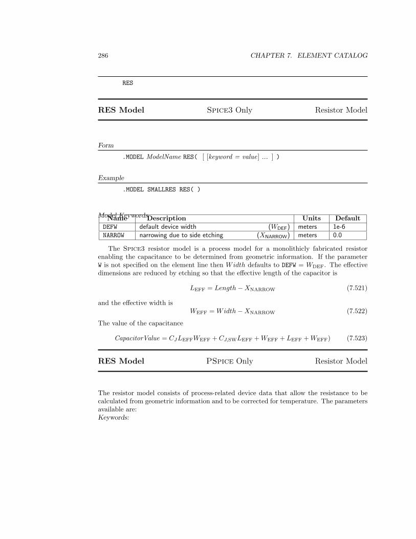
286 CHAPTER 7. ELEMENT CATALOG
RES
RES Model Spice3 Only Resistor Model
Form
.MODEL ModelName RES( [ [keyword = value] ... ] )
Example
.MODEL SMALLRES RES( )
Model KeywordsName Description Units DefaultDEFW default device width (WDEF) meters 1e-6NARROW narrowing due to side etching (XNARROW) meters 0.0
The Spice3 resistor model is a process model for a monolithicly fabricated resistorenabling the capacitance to be determined from geometric information. If the parameterW is not specified on the element line then Width defaults to DEFW = WDEF. The effectivedimensions are reduced by etching so that the effective length of the capacitor is
LEFF = Length−XNARROW (7.521)
and the effective width isWEFF = Width−XNARROW (7.522)
The value of the capacitance
CapacitorValue = CJLEFFWEFF + CJ,SWLEFF + WEFF + LEFF + WEFF) (7.523)
RES Model PSpice Only Resistor Model
The resistor model consists of process-related device data that allow the resistance to becalculated from geometric information and to be corrected for temperature. The parametersavailable are:Keywords:
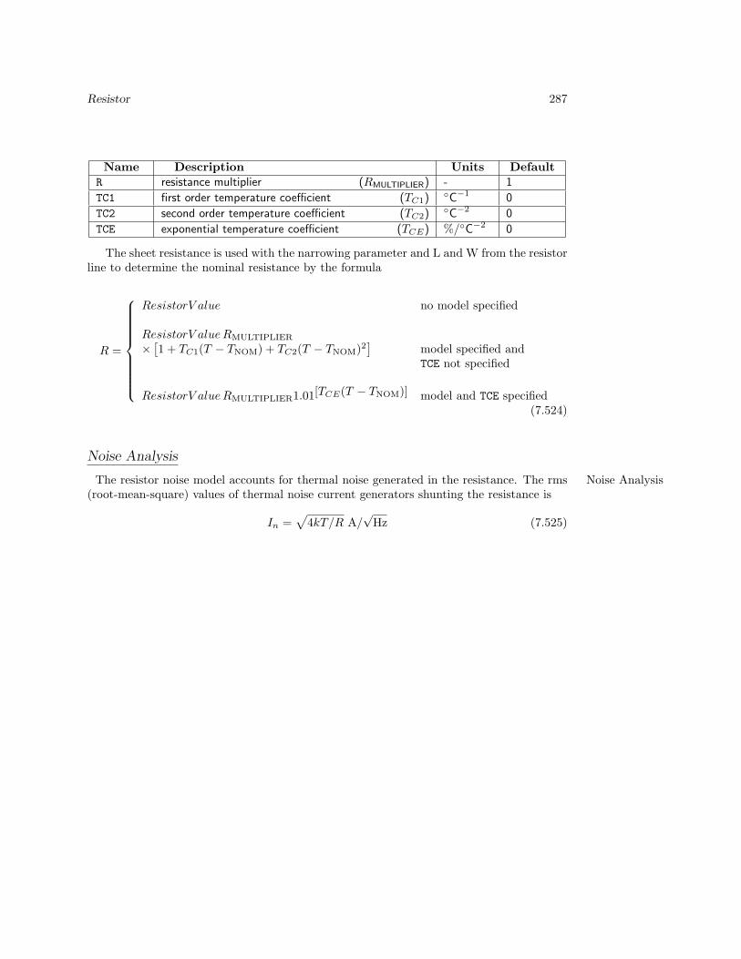
Resistor 287
Name Description Units DefaultR resistance multiplier (RMULTIPLIER) - 1
TC1 first order temperature coefficient (TC1)C−1 0
TC2 second order temperature coefficient (TC2)C−2 0
TCE exponential temperature coefficient (TCE) %/C−2 0
The sheet resistance is used with the narrowing parameter and L and W from the resistorline to determine the nominal resistance by the formula
R =
ResistorV alue no model specified
ResistorV alueRMULTIPLIER
× [1 + TC1(T − TNOM) + TC2(T − TNOM)2
]model specified andTCE not specified
ResistorV alueRMULTIPLIER1.01[TCE(T − TNOM)] model and TCE specified(7.524)
Noise Analysis
The resistor noise model accounts for thermal noise generated in the resistance. The rms Noise Analysis(root-mean-square) values of thermal noise current generators shunting the resistance is
In =√
4kT/R A/√
Hz (7.525)
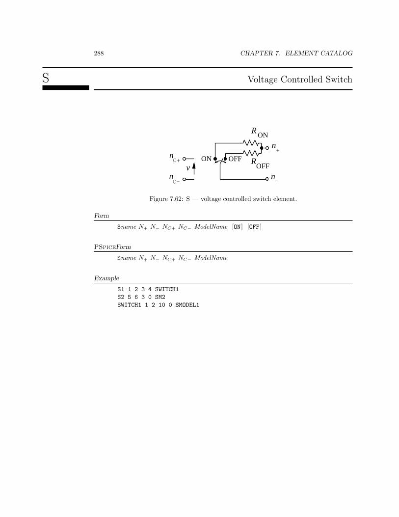
288 CHAPTER 7. ELEMENT CATALOG
S Voltage Controlled Switch
n+
n-
nC+
nC-
v
RON
ROFF
ON OFF
Figure 7.62: S — voltage controlled switch element.
Form
Sname N+ N− NC+ NC− ModelName [ON] [OFF]
PSpiceForm
Sname N+ N− NC+ NC− ModelName
Example
S1 1 2 3 4 SWITCH1S2 5 6 3 0 SM2SWITCH1 1 2 10 0 SMODEL1
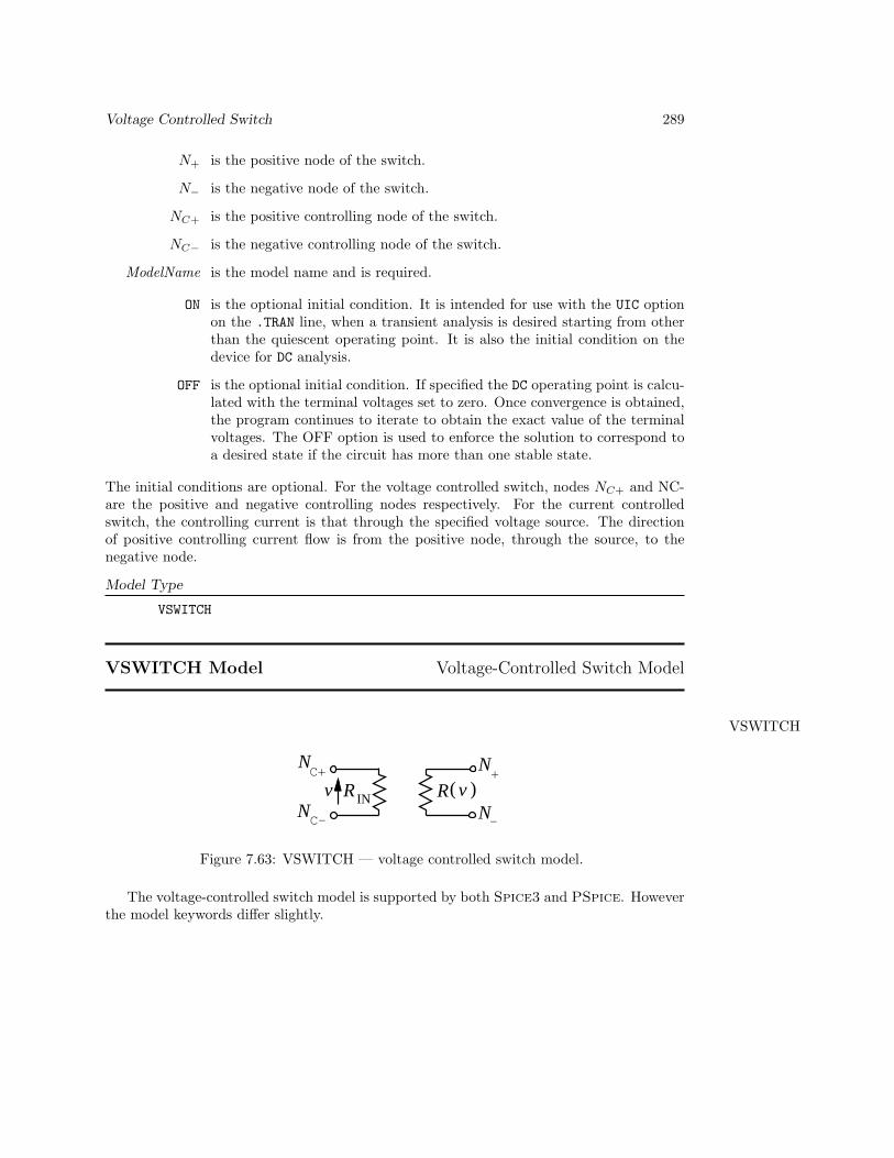
Voltage Controlled Switch 289
N+ is the positive node of the switch.
N− is the negative node of the switch.
NC+ is the positive controlling node of the switch.
NC− is the negative controlling node of the switch.
ModelName is the model name and is required.
ON is the optional initial condition. It is intended for use with the UIC optionon the .TRAN line, when a transient analysis is desired starting from otherthan the quiescent operating point. It is also the initial condition on thedevice for DC analysis.
OFF is the optional initial condition. If specified the DC operating point is calcu-lated with the terminal voltages set to zero. Once convergence is obtained,the program continues to iterate to obtain the exact value of the terminalvoltages. The OFF option is used to enforce the solution to correspond toa desired state if the circuit has more than one stable state.
The initial conditions are optional. For the voltage controlled switch, nodes NC+ and NC-are the positive and negative controlling nodes respectively. For the current controlledswitch, the controlling current is that through the specified voltage source. The directionof positive controlling current flow is from the positive node, through the source, to thenegative node.
Model Type
VSWITCH
VSWITCH Model Voltage-Controlled Switch Model
VSWITCH
+
-
C+
C-
v R( )vR IN
N
N N
N
Figure 7.63: VSWITCH — voltage controlled switch model.
The voltage-controlled switch model is supported by both Spice3 and PSpice. Howeverthe model keywords differ slightly.
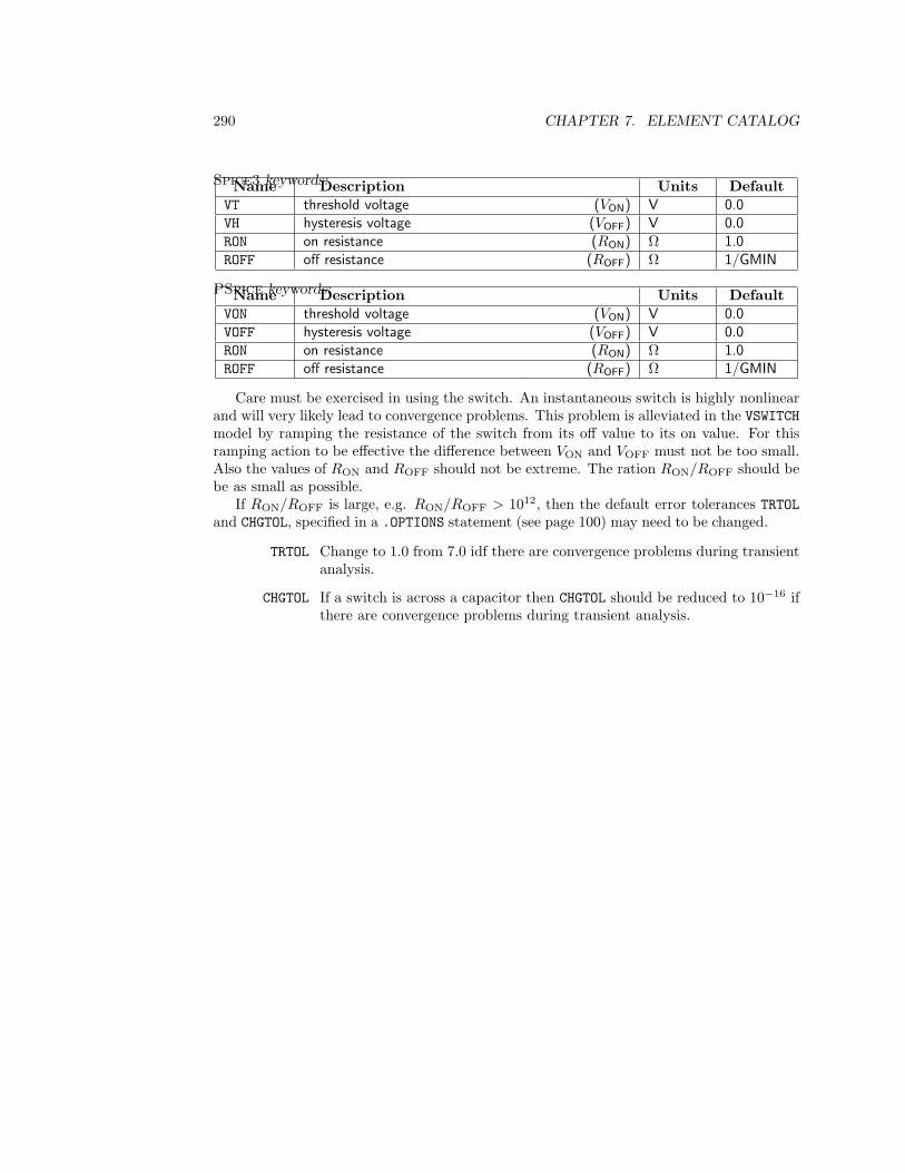
290 CHAPTER 7. ELEMENT CATALOG
Spice3 keywords:Name Description Units DefaultVT threshold voltage (VON) V 0.0VH hysteresis voltage (VOFF) V 0.0RON on resistance (RON) Ω 1.0ROFF off resistance (ROFF) Ω 1/GMIN
PSpice keywords:Name Description Units DefaultVON threshold voltage (VON) V 0.0VOFF hysteresis voltage (VOFF) V 0.0RON on resistance (RON) Ω 1.0ROFF off resistance (ROFF) Ω 1/GMIN
Care must be exercised in using the switch. An instantaneous switch is highly nonlinearand will very likely lead to convergence problems. This problem is alleviated in the VSWITCHmodel by ramping the resistance of the switch from its off value to its on value. For thisramping action to be effective the difference between VON and VOFF must not be too small.Also the values of RON and ROFF should not be extreme. The ration RON/ROFF should bebe as small as possible.
If RON/ROFF is large, e.g. RON/ROFF > 1012, then the default error tolerances TRTOLand CHGTOL, specified in a .OPTIONS statement (see page 100) may need to be changed.
TRTOL Change to 1.0 from 7.0 idf there are convergence problems during transientanalysis.
CHGTOL If a switch is across a capacitor then CHGTOL should be reduced to 10−16 ifthere are convergence problems during transient analysis.
Voltage Controlled Switch 291
SSwitch Model
The switch is modeled by a voltage variable resistor R and an input input resistanceRIN, see figure 7.63. RIN = 1/GMIN to ensure that the controlling nodes are not floatingand that the voltage v between the controlling nodes can not change instantaneously.GMIN = GMIN is described on page ??.
Standard Calculations
RMEAN =√
RON + ROFF (7.526)RRATIO = RON/ROFF (7.527)
VMEAN =√
VON + VOFF (7.528)
V∆ =(
v − VMEAN
VON − VOFF
)(7.529)
If VON > VOFF the switch resistance
R =
RON v ≥ VON
ROFF v ≤ VOFF
RMEAN R1.5V∆RATIO R
1.5V 3∆
RATIO VOFF < v < VON
(7.530)
If VON < VOFF the switch resistance
R =
RON v ≤ VON
ROFF v ≥ VOFF
RMEAN R1.5V∆RATIO R
1.5V 3∆
RATIO VOFF < v < VON
(7.531)
Noise Analysis
The voltage controlled switch noise model accounts for thermal noise generated in the Noise Analysisswitch resistance. The rms (root-mean-square) values of thermal noise current generatorsshunting the switch resistance is Noise Model
In =√
4kT/R A/√
Hz (7.532)
where T is the analysis temperature in kelvin (K), and k (= 1.3806226 10−23 J/K) is Boltz-mans constant.

292 CHAPTER 7. ELEMENT CATALOG
T Transmission Line
n1
n2
n3
n4
Z0 , TD
Figure 7.64: T — transmission line element.
Form
Tname n1 n2 n3 n4 Z0=CharacteristicImpedance TD=TimeDelay [IC=V1, I1, V2, I2
]
Tname n1 n2 n3 n4 Z0=CharacteristicImpedance F=ReferenceFrequency+ [NL=NormalizedElectricalLength] [IC=V1, I1, V2, I2 ]
Spice3Form
Tname n1 n2 n3 n4 [ModelName ] Z0=CharacteristicImpedance TD=TimeDelay[IC=V1, I1, V2, I2 ]
Tname n1 n2 n3 n4 [ModelName ] Z0=CharacteristicImpedance+ F=ReferenceFrequency + [NL=NormalizedElectricalLength] [IC=V1, I1, V2, I2 ]
PSpiceForm
Tname n1 n2 n3 n4 Z0=CharacteristicImpedance TD=TimeDelay
Tname n1 n2 n3 n4 Z0=CharacteristicImpedance+F=Frequency [NL=NormalizedElectricalLength]

Transmission Line 293
n1 positive node at port 1.
n2 negative node at port 1.
n3 positive node at port 2.
n4 negative node at port 2.
ModelName is the model name.
Z0 is the characteristic impedance. (Z-zero)(Units: Ω; Required; Symbol: Z0; Default: none)
TD transmission line delay. (Units: s; Either TD or F Required; Symbol: TD;Default: none)
F reference frequency. (Units: Hz; Either TD or F Required; Symbol: F ;Default: none)
NL normalized electrical length. Normalization is with respect to the wave-length in free space at the reference frequency F.(Units: none; Optional; Symbol: LNORMALIZED; Default: 0.25)
IC is the optional initial condition specification using IC= V1, I1, V2, I2 is in-tended for use with the UIC option on the .TRAN line, when a transientanalysis is desired starting from other than the quiescent operating point.Specification of the transient initial conditions using the .IC statement (seepage 83) is preferred and is more convenient.
Example
T1 1 0 2 0 Z0=50 TD=10NS
TLONG 1 0 2 0 Z0=50 F=1G NL=10
TLONG 1 0 2 0 Z0=50 F=1G
Note

294 CHAPTER 7. ELEMENT CATALOG
1. The length of the line may be expressed in either of two forms. The transmission delay,TD, may be specified directly (as TD=10ns, for example). Alternatively, a frequencyF may be given, together with NL, the normalized electrical length of the transmissionline with respect to the wavelength in the line at the frequency F. If a frequency isspecified but NL is omitted, 0.25 is assumed (that is, the frequency is assumed to bethe quarter-wave frequency). Note that although both forms for expressing the linelength are indicated as optional, one of the two must be specified.
2. Note that only 3 distinct nodes should be specified as this element describes a singlepropagating mode. With four distinct nodes specified, two propagating modes mayexist on the actual line. If there are four distinct nodes then two lines are required.
3. The transmission line T element is modeled as a bidirectional ideal delay element asshown in figure 7.65. The maximum time step in Spice is limited to half of the timedelay along the line. Thus short transmission lines can result in many time steps in atransient analysis. Unnecessary short transmission lines should be avoided.
tmodel.ps
Figure 7.65: Ideal bidirectional delay element model of the transmission line T element.
Model Type
URC
URC Model Lossy RC Transmission Line Model
urc.ps
Figure 7.66: URC — lossy RC transmission line model: (a) linear RC transmission linemodel; (b) nonlinear transmission line model.
Form
.MODEL ModelName URC( [ [keyword = value] ... ] )
Example
.MODEL LONGLINE URC( )
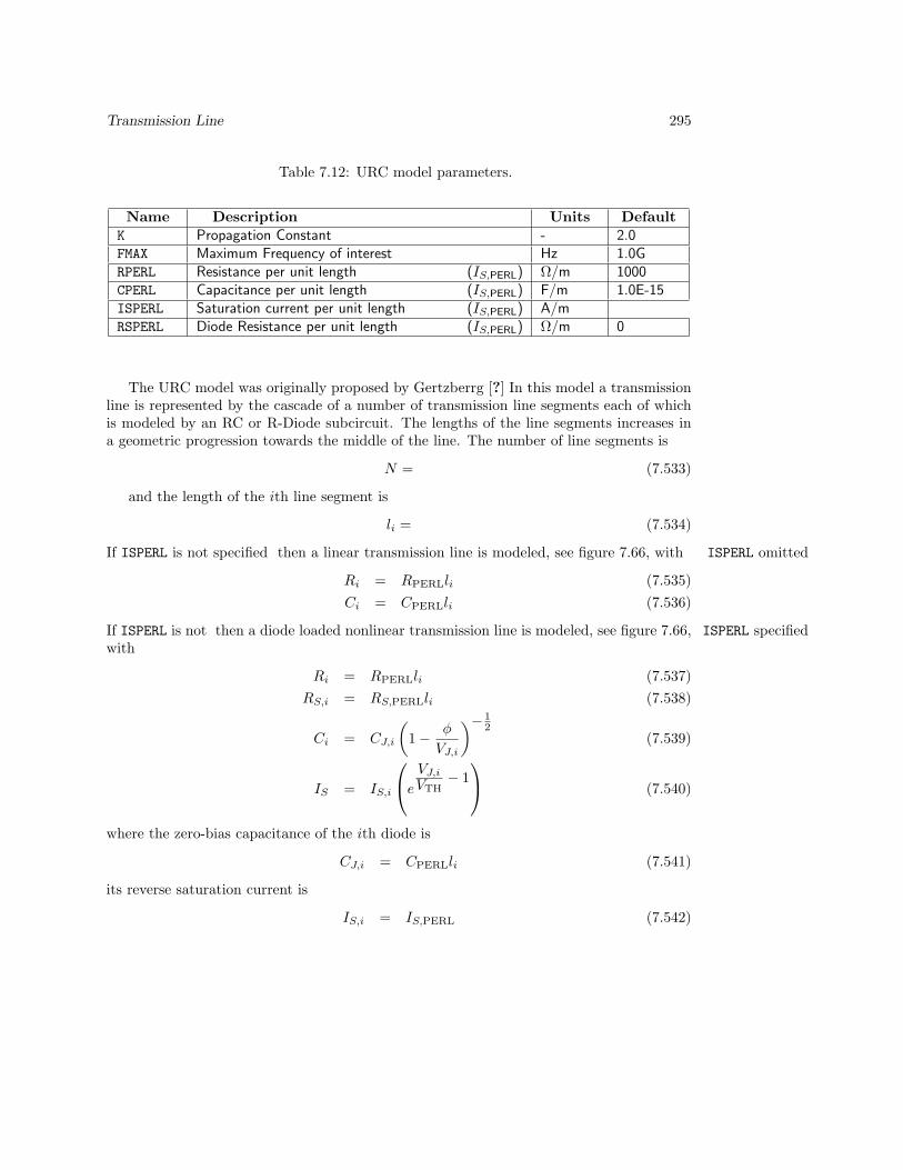
Transmission Line 295
Table 7.12: URC model parameters.
Name Description Units DefaultK Propagation Constant - 2.0FMAX Maximum Frequency of interest Hz 1.0GRPERL Resistance per unit length (IS,PERL) Ω/m 1000CPERL Capacitance per unit length (IS,PERL) F/m 1.0E-15ISPERL Saturation current per unit length (IS,PERL) A/mRSPERL Diode Resistance per unit length (IS,PERL) Ω/m 0
The URC model was originally proposed by Gertzberrg [?] In this model a transmissionline is represented by the cascade of a number of transmission line segments each of whichis modeled by an RC or R-Diode subcircuit. The lengths of the line segments increases ina geometric progression towards the middle of the line. The number of line segments is
N = (7.533)
and the length of the ith line segment is
li = (7.534)
If ISPERL is not specified then a linear transmission line is modeled, see figure 7.66, with ISPERL omitted
Ri = RPERLli (7.535)Ci = CPERLli (7.536)
If ISPERL is not then a diode loaded nonlinear transmission line is modeled, see figure 7.66, ISPERL specifiedwith
Ri = RPERLli (7.537)RS,i = RS,PERLli (7.538)
Ci = CJ,i
(1− φ
VJ,i
)− 12
(7.539)
IS = IS,i
e
VJ,i
VTH− 1
(7.540)
where the zero-bias capacitance of the ith diode is
CJ,i = CPERLli (7.541)
its reverse saturation current is
IS,i = IS,PERL (7.542)

296 CHAPTER 7. ELEMENT CATALOG
U PSpiceonly Digital Device
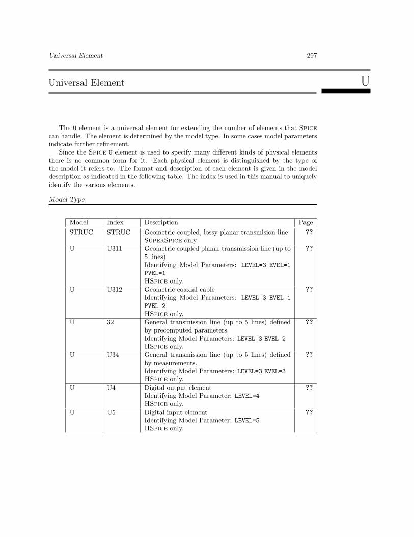
Universal Element 297
Universal Element U
The U element is a universal element for extending the number of elements that Spicecan handle. The element is determined by the model type. In some cases model parametersindicate further refinement.
Since the Spice U element is used to specify many different kinds of physical elementsthere is no common form for it. Each physical element is distinguished by the type ofthe model it refers to. The format and description of each element is given in the modeldescription as indicated in the following table. The index is used in this manual to uniquelyidentify the various elements.
Model Type
Model Index Description PageSTRUC STRUC Geometric coupled, lossy planar transmision line
SuperSpice only.??
U U311 Geometric coupled planar transmission line (up to5 lines)Identifying Model Parameters: LEVEL=3 EVEL=1PVEL=1HSpice only.
??
U U312 Geometric coaxial cableIdentifying Model Parameters: LEVEL=3 EVEL=1PVEL=2HSpice only.
??
U 32 General transmission line (up to 5 lines) definedby precomputed parameters.Identifying Model Parameters: LEVEL=3 EVEL=2HSpice only.
??
U U34 General transmission line (up to 5 lines) definedby measurements.Identifying Model Parameters: LEVEL=3 EVEL=3HSpice only.
??
U U4 Digital output elementIdentifying Model Parameter: LEVEL=4HSpice only.
??
U U5 Digital input elementIdentifying Model Parameter: LEVEL=5HSpice only.
??
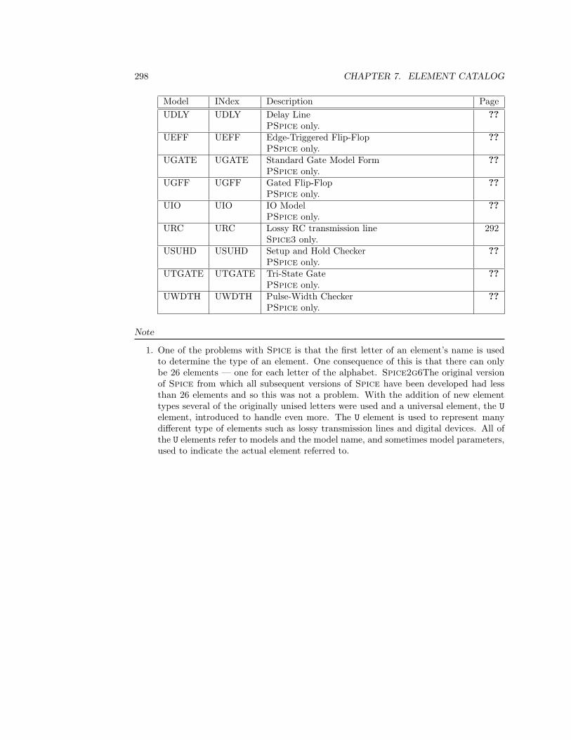
298 CHAPTER 7. ELEMENT CATALOG
Model INdex Description PageUDLY UDLY Delay Line
PSpice only.??
UEFF UEFF Edge-Triggered Flip-FlopPSpice only.
??
UGATE UGATE Standard Gate Model FormPSpice only.
??
UGFF UGFF Gated Flip-FlopPSpice only.
??
UIO UIO IO ModelPSpice only.
??
URC URC Lossy RC transmission lineSpice3 only.
292
USUHD USUHD Setup and Hold CheckerPSpice only.
??
UTGATE UTGATE Tri-State GatePSpice only.
??
UWDTH UWDTH Pulse-Width CheckerPSpice only.
??
Note
1. One of the problems with Spice is that the first letter of an element’s name is usedto determine the type of an element. One consequence of this is that there can onlybe 26 elements — one for each letter of the alphabet. Spice2g6The original versionof Spice from which all subsequent versions of Spice have been developed had lessthan 26 elements and so this was not a problem. With the addition of new elementtypes several of the originally unised letters were used and a universal element, the Uelement, introduced to handle even more. The U element is used to represent manydifferent type of elements such as lossy transmission lines and digital devices. All ofthe U elements refer to models and the model name, and sometimes model parameters,used to indicate the actual element referred to.
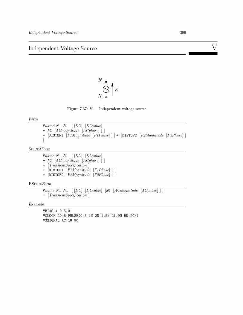
Independent Voltage Source 299
Independent Voltage Source V
E
-
+N
N
Figure 7.67: V — Independent voltage source.
Form
Vname N+ N− [ [DC] [DCvalue]+ [AC [ACmagnitude [ACphase] ] ]+ [DISTOF1 [F1Magnitude [F1Phase] ] ] + [DISTOF2 [F2Magnitude [F2Phase] ]]
Spice3Form
Vname N+ N− [ [DC] [DCvalue]+ [AC [ACmagnitude [ACphase] ] ]+ [TransientSpecification ]+ [DISTOF1 [F1Magnitude [F1Phase] ] ]+ [DISTOF2 [F2Magnitude [F2Phase] ] ]
PSpiceForm
Vname N+ N− [ [DC] [DCvalue] [AC [ACmagnitude [ACphase] ] ]+ [TransientSpecification ]
Example
VBIAS 1 0 5.0VCLOCK 20 5 PULSE(0 5 1N 2N 1.5N 21.9N 5N 20N)VSSIGNAL AC 1U 90
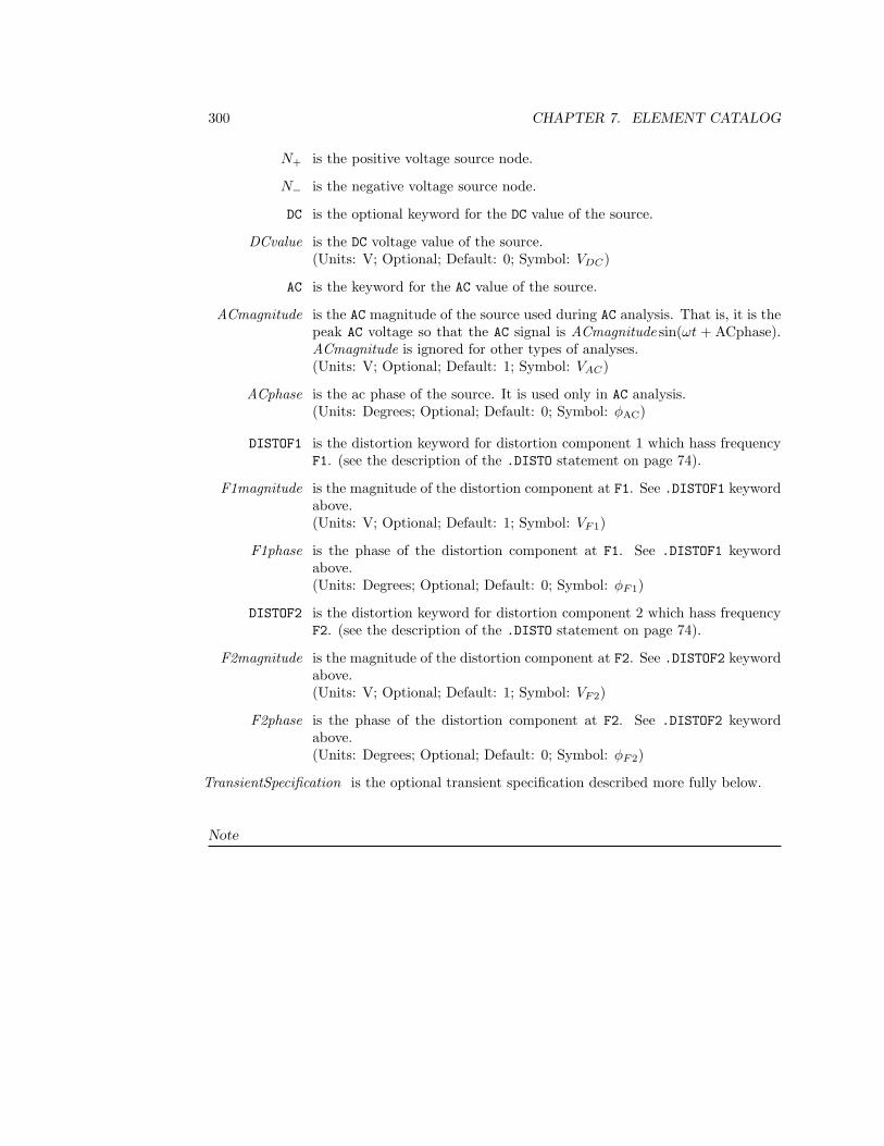
300 CHAPTER 7. ELEMENT CATALOG
N+ is the positive voltage source node.
N− is the negative voltage source node.
DC is the optional keyword for the DC value of the source.
DCvalue is the DC voltage value of the source.(Units: V; Optional; Default: 0; Symbol: VDC)
AC is the keyword for the AC value of the source.
ACmagnitude is the AC magnitude of the source used during AC analysis. That is, it is thepeak AC voltage so that the AC signal is ACmagnitude sin(ωt + ACphase).ACmagnitude is ignored for other types of analyses.(Units: V; Optional; Default: 1; Symbol: VAC)
ACphase is the ac phase of the source. It is used only in AC analysis.(Units: Degrees; Optional; Default: 0; Symbol: φAC)
DISTOF1 is the distortion keyword for distortion component 1 which hass frequencyF1. (see the description of the .DISTO statement on page 74).
F1magnitude is the magnitude of the distortion component at F1. See .DISTOF1 keywordabove.(Units: V; Optional; Default: 1; Symbol: VF1)
F1phase is the phase of the distortion component at F1. See .DISTOF1 keywordabove.(Units: Degrees; Optional; Default: 0; Symbol: φF1)
DISTOF2 is the distortion keyword for distortion component 2 which hass frequencyF2. (see the description of the .DISTO statement on page 74).
F2magnitude is the magnitude of the distortion component at F2. See .DISTOF2 keywordabove.(Units: V; Optional; Default: 1; Symbol: VF2)
F2phase is the phase of the distortion component at F2. See .DISTOF2 keywordabove.(Units: Degrees; Optional; Default: 0; Symbol: φF2)
TransientSpecification is the optional transient specification described more fully below.
Note
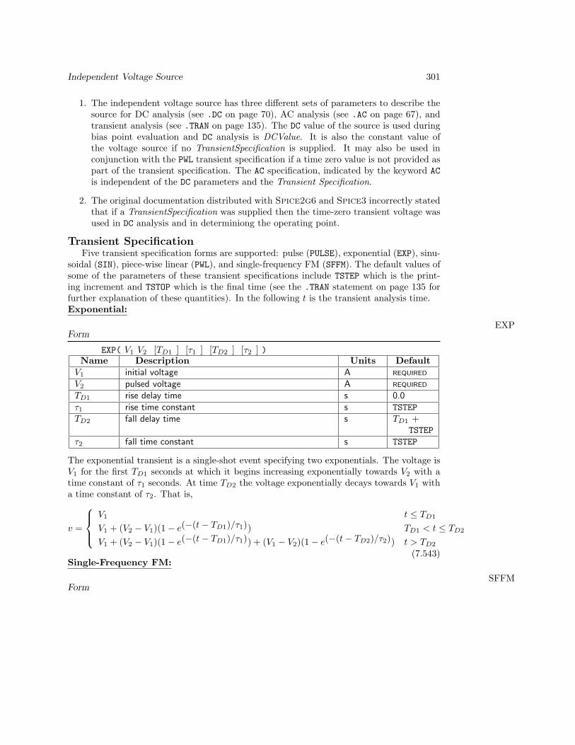
Independent Voltage Source 301
1. The independent voltage source has three different sets of parameters to describe thesource for DC analysis (see .DC on page 70), AC analysis (see .AC on page 67), andtransient analysis (see .TRAN on page 135). The DC value of the source is used duringbias point evaluation and DC analysis is DCValue. It is also the constant value ofthe voltage source if no TransientSpecification is supplied. It may also be used inconjunction with the PWL transient specification if a time zero value is not provided aspart of the transient specification. The AC specification, indicated by the keyword ACis independent of the DC parameters and the Transient Specification.
2. The original documentation distributed with Spice2g6 and Spice3 incorrectly statedthat if a TransientSpecification was supplied then the time-zero transient voltage wasused in DC analysis and in determiniong the operating point.
Transient SpecificationFive transient specification forms are supported: pulse (PULSE), exponential (EXP), sinu-
soidal (SIN), piece-wise linear (PWL), and single-frequency FM (SFFM). The default values ofsome of the parameters of these transient specifications include TSTEP which is the print-ing increment and TSTOP which is the final time (see the .TRAN statement on page 135 forfurther explanation of these quantities). In the following t is the transient analysis time.Exponential:
EXPForm
EXP( V1 V2 [TD1 ] [τ1 ] [TD2 ] [τ2 ] )Name Description Units Default
V1 initial voltage A REQUIRED
V2 pulsed voltage A REQUIRED
TD1 rise delay time s 0.0τ1 rise time constant s TSTEPTD2 fall delay time s TD1 +
TSTEPτ2 fall time constant s TSTEP
The exponential transient is a single-shot event specifying two exponentials. The voltage isV1 for the first TD1 seconds at which it begins increasing exponentially towards V2 with atime constant of τ1 seconds. At time TD2 the voltage exponentially decays towards V1 witha time constant of τ2. That is,
v =
V1 t ≤ TD1
V1 + (V2 − V1)(1− e(−(t− TD1)/τ1)) TD1 < t ≤ TD2
V1 + (V2 − V1)(1− e(−(t− TD1)/τ1)) + (V1 − V2)(1− e(−(t− TD2)/τ2)) t > TD2
(7.543)Single-Frequency FM:
SFFMForm
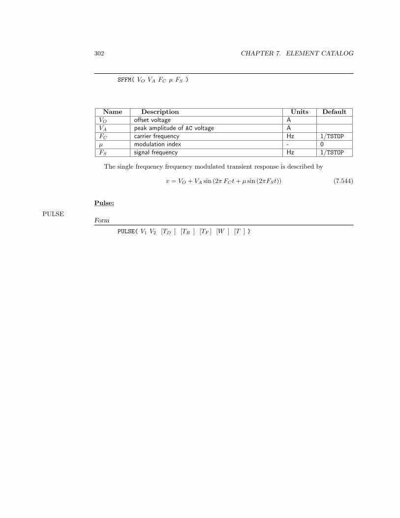
302 CHAPTER 7. ELEMENT CATALOG
SFFM( VO VA FC µ FS )
Name Description Units DefaultVO offset voltage AVA peak amplitude of AC voltage AFC carrier frequency Hz 1/TSTOPµ modulation index - 0FS signal frequency Hz 1/TSTOP
The single frequency frequency modulated transient response is described by
v = VO + VA sin (2π FCt + µ sin (2πFSt)) (7.544)
Pulse:
PULSEForm
PULSE( V1 V2 [TD ] [TR ] [TF ] [W ] [T ] )
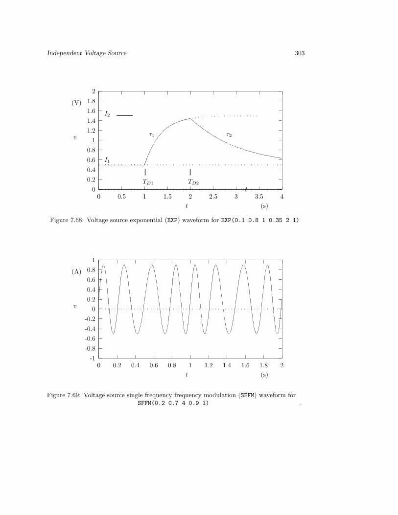
Independent Voltage Source 303
00.20.40.60.8
11.21.41.61.8
2
0 0.5 1 1.5 2 2.5 3 3.5 4
I2
I1
τ1 τ2
TD1 TD2
t
v
(V)
t (s)
Figure 7.68: Voltage source exponential (EXP) waveform for EXP(0.1 0.8 1 0.35 2 1)
-1-0.8-0.6-0.4-0.2
00.20.40.60.8
1
0 0.2 0.4 0.6 0.8 1 1.2 1.4 1.6 1.8 2
v
(A)
t (s)
Figure 7.69: Voltage source single frequency frequency modulation (SFFM) waveform forSFFM(0.2 0.7 4 0.9 1) .

304 CHAPTER 7. ELEMENT CATALOG
Name Description Units DefaultV1 initial voltage A REQUIRED
V2 pulsed voltage A REQUIRED
TD delay time s 0.0TR rise time s TSTEPTF fall time s TSTEPW pulse width s TSTOPT period s TSTOP
The pulse transient waveform is defined by
v =
V1 t ≤ TD
V1 + t′TR
(V2 − V1) 0 < t′ ≤ TR
V2 TR < t′ < (TR + W )V2 − t′ −W
TF(V1 − V2) (TR + W ) < t′ < (TR + W + TF )
V1 (TR + W + TF ) < t′ < T
(7.545)
wheret′ = t− TD − (n− 1)T (7.546)
and t is the voltage analysis time and n is the cycle index. The effect of this is that afteran initial time delay TD the transient waveform repeats itself every cycle.Piece-Wise Linear:
PWLForm
PWL( T1 V1 [T2 V2 ... Ti Vi ... TN VN ] )
Each pair of values (Ti, Vi) specifies that the value of the source is Vi at time = Ti. Attimes between Ti and Ti+1 the values are linearly interpolated. If T1 > 0 then the voltageis constant at DCValue (specified on the element line) until time T1.
v =
DCvalue t < T1
Vi t = Ti
Vi+1 t = Ti+1
Vi +(
t−Ti
Ti+1−Ti
)(Vi+1 − Vi) Ti < t ≤ Ti+1
VN t > TN
(7.547)
Sinusoidal:
SINForm
SIN( VO VA [F ] [TD ] [θ ] )
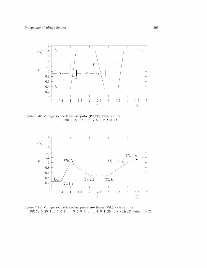
Independent Voltage Source 305
00.20.40.60.8
11.21.41.61.8
2
0 0.5 1 1.5 2 2.5 3 3.5 4 4.5 5
i
(A)
t (s)
I2
I1
TD←− −→TR
TFW←− −→
←− T −→
Figure 7.70: Voltage source transient pulse (PULSE) waveform forPULSE(0.3 1.8 1 2.5 0.3 1 0.7)
00.20.40.60.8
11.21.41.61.8
2
0 0.5 1 1.5 2 2.5 3 3.5 4 4.5 5
•
IDC
(T1, I1)
v
(A)
t (s)
(T2, I2)
(T3, I3) (Ti, Ii)
(Ti+1, Ii+1)
(TN , IN )
Figure 7.71: Voltage source transient piece-wise linear (PWL) waveform forPWL(1 0.25 1 1 2 0.5 . . . 3 0.5 4 1 . . . 4.5 1.25 . . .) with DCValue = 0.25.
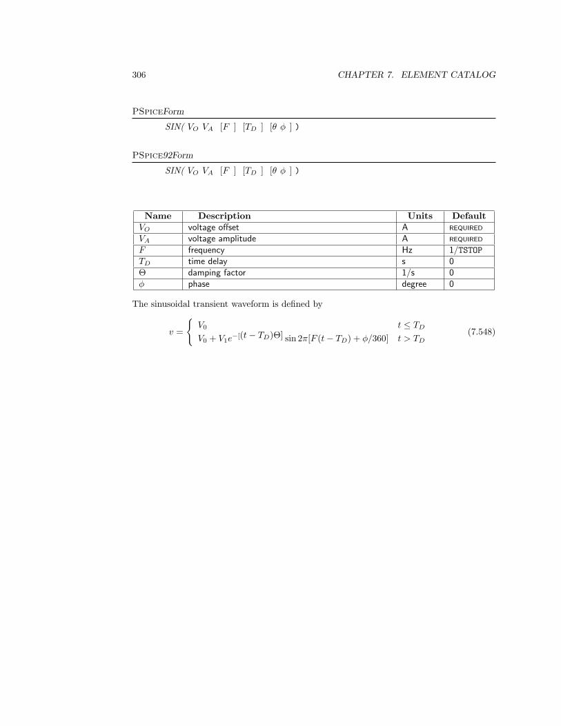
306 CHAPTER 7. ELEMENT CATALOG
PSpiceForm
SIN( VO VA [F ] [TD ] [θ φ ] )
PSpice92Form
SIN( VO VA [F ] [TD ] [θ φ ] )
Name Description Units DefaultVO voltage offset A REQUIRED
VA voltage amplitude A REQUIRED
F frequency Hz 1/TSTOPTD time delay s 0Θ damping factor 1/s 0φ phase degree 0
The sinusoidal transient waveform is defined by
v =
V0 t ≤ TD
V0 + V1e−[(t− TD)Θ] sin 2π[F (t− TD) + φ/360] t > TD
(7.548)

Independent Voltage Source 307
-1-0.8-0.6-0.4-0.2
00.20.40.60.8
1
0 0.5 1 1.5 2 2.5 3 3.5 4
v
(A)
t (s)
Figure 7.72: Voltage source transient sine (SIN) waveform for SIN(0.1 0.8 2 1 0.3 ).
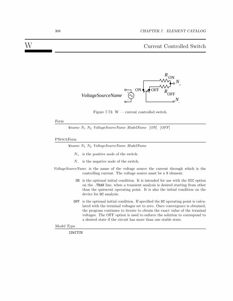
308 CHAPTER 7. ELEMENT CATALOG
W Current Controlled Switch
+
-
RON
ROFF
ON OFF+
-VoltageSourceName
N
N
Figure 7.73: W — current controlled switch.
Form
Wname N1 N2 VoltageSourceName ModelName [ON] [OFF]
PSpiceForm
Wname N1 N2 VoltageSourceName ModelName
N+ is the positive node of the switch.
N− is the negative node of the switch.
VoltageSourceName is the name of the voltage source the current through which is thecontrolling current. The voltage source must be a V element.
ON is the optional initial condition. It is intended for use with the UIC optionon the .TRAN line, when a transient analysis is desired starting from otherthan the quiescent operating point. It is also the initial condition on thedevice for DC analysis.
OFF is the optional initial condition. If specified the DC operating point is calcu-lated with the terminal voltages set to zero. Once convergence is obtained,the program continues to iterate to obtain the exact value of the terminalvoltages. The OFF option is used to enforce the solution to correspond toa desired state if the circuit has more than one stable state.
Model Type
ISWITCH
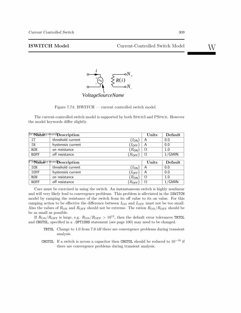
Current Controlled Switch 309
WISWITCH Model Current-Controlled Switch Model
+
-
R+
-
i
i( )
VoltageSourceName
N
N
Figure 7.74: ISWITCH — current controlled switch model.
The current-controlled switch model is supported by both Spice3 and PSpice. Howeverthe model keywords differ slightly.
Spice3 keywords:Name Description Units DefaultIT threshold current (ION) A 0.0IH hysteresis current (IOFF) A 0.0RON on resistance (RON) Ω 1.0ROFF off resistance (ROFF) Ω 1/GMIN
PSpice keywords:Name Description Units DefaultION threshold current (ION) A 0.0IOFF hysteresis current (IOFF) A 0.0RON on resistance (RON) Ω 1.0ROFF off resistance (ROFF) Ω 1/GMIN
Care must be exercised in using the switch. An instantaneous switch is highly nonlinearand will very likely lead to convergence problems. This problem is alleviated in the ISWITCHmodel by ramping the resistance of the switch from its off value to its on value. For thisramping action to be effective the difference between ION and IOFF must not be too small.Also the values of RON and ROFF should not be extreme. The ration RON/ROFF should bebe as small as possible.
If RON/ROFF is large, e.g. RON/ROFF > 1012, then the default error tolerances TRTOLand CHGTOL, specified in a .OPTIONS statement (see page 100) may need to be changed.
TRTOL Change to 1.0 from 7.0 idf there are convergence problems during transientanalysis.
CHGTOL If a switch is across a capacitor then CHGTOL should be reduced to 10−16 ifthere are convergence problems during transient analysis.
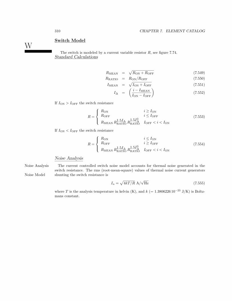
310 CHAPTER 7. ELEMENT CATALOG
WSwitch Model
The switch is modeled by a current variable resistor R, see figure 7.74.Standard Calculations
RMEAN =√
RON + ROFF (7.549)RRATIO = RON/ROFF (7.550)
IMEAN =√
ION + IOFF (7.551)
I∆ =(
i− IMEAN
ION − IOFF
)(7.552)
If ION > IOFF the switch resistance
R =
RON i ≥ ION
ROFF i ≤ IOFF
RMEAN R1.5I∆RATIO R
1.5I3∆
RATIO IOFF < i < ION
(7.553)
If ION < IOFF the switch resistance
R =
RON i ≤ ION
ROFF i ≥ IOFF
RMEAN R1.5I∆RATIO R
1.5I3∆
RATIO IOFF < i < ION
(7.554)
Noise Analysis
The current controlled switch noise model accounts for thermal noise generated in theNoise Analysisswitch resistance. The rms (root-mean-square) values of thermal noise current generatorsshunting the switch resistance isNoise Model
In =√
4kT/R A/√
Hz (7.555)
where T is the analysis temperature in kelvin (K), and k (= 1.3806226 10−23 J/K) is Boltz-mans constant.

Subcircuit Call 311
Subcircuit Call X
Form
1
2
3SUBCIRCUIT
SubcircuitName
NN
NNN
Figure 7.75: X — subcircuit call element.
Xname N1 [N2 N3 ... NN ] SubcircuitName
PSpiceForm
Xname N1 [N2 N3 ... NN ] SubcircuitName [PARAMS: [keyword = Expression . . . ] [Keyword = Value . . . ] ]
N1 is the first node of the subcircuit.
NN is the Nth node of the subcircuit.
SubcircuitName is the name of the subcircuit.
PARAMS: indicates that parameters are to be passed to the subcircuit.
keyword: is keyword corresponding to the keywords defined in the .SUBCKT statement.(See page 128).
value: is numeric value.
Expression: is an algebraic expression which evaluates to a numeric value. .SUBCKTstatement. (See section ?? on page ??).
Example
X1 2 4 17 3 1 MULTI

312 CHAPTER 7. ELEMENT CATALOG
Subcircuits are incorporated by using the “X” element. The number of nodes of the “X”element must correspond to the number of nodes in the definition of the subcircuit (i.e. ison the .SUBCKT statement (see page 128).
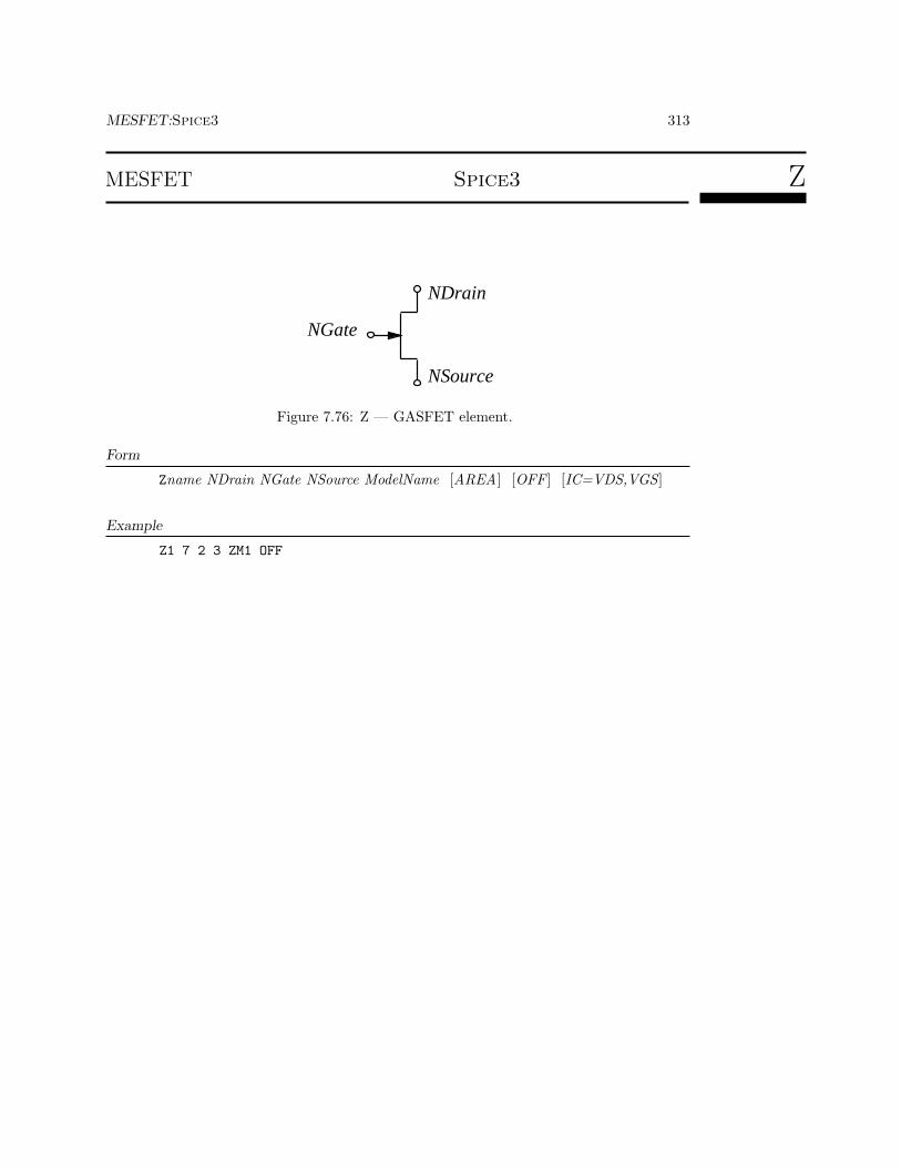
MESFET:Spice3 313
MESFET Spice3 Z
NGate
NDrain
NSource
Figure 7.76: Z — GASFET element.
Form
Zname NDrain NGate NSource ModelName [AREA] [OFF] [IC=VDS,VGS]
Example
Z1 7 2 3 ZM1 OFF

314 CHAPTER 7. ELEMENT CATALOG
NDrain is the drain node.
NGate is the gate node.
NSource is the source node.
ModelName is the model name.
OFF indicates an (optional) initial condition on the device for DC analysis. Ifspecified the DC operating point is calculated with the terminal voltages setto zero. Once convergence is obtained, the program continues to iterate toobtain the exact value of the terminal voltages. The OFF option is used toenforce the solution to correspond to a desired state if the circuit has morethan one stable state.
IC is the optional initial condition specification. Using IC=VDS , VGS , VBS isintended for use with the UIC option on the .TRAN line, when a transientanalysis is desired starting from other than the quiescent operating point.Specification of the transient initial conditions using the .IC statement (seepage 83) is preferred and is more convenient.
Model Type
GASFET
GASFET Model GaAs MESFET Model
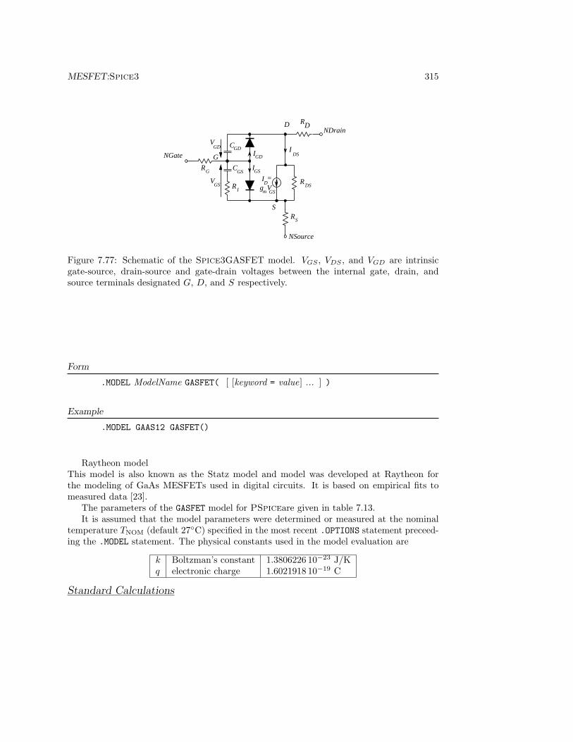
MESFET:Spice3 315
NGate G
S
NSource
NDrainD
RG
RDS
IDS
VGS
CGS
RI
IGD
IGS
g Vm GS
ID=
RS
RD
CGDV
GD
Figure 7.77: Schematic of the Spice3GASFET model. VGS , VDS , and VGD are intrinsicgate-source, drain-source and gate-drain voltages between the internal gate, drain, andsource terminals designated G, D, and S respectively.
Form
.MODEL ModelName GASFET( [ [keyword = value] ... ] )
Example
.MODEL GAAS12 GASFET()
Raytheon modelThis model is also known as the Statz model and model was developed at Raytheon forthe modeling of GaAs MESFETs used in digital circuits. It is based on empirical fits tomeasured data [23].
The parameters of the GASFET model for PSpiceare given in table 7.13.It is assumed that the model parameters were determined or measured at the nominal
temperature TNOM (default 27C) specified in the most recent .OPTIONS statement preceed-ing the .MODEL statement. The physical constants used in the model evaluation are
k Boltzman’s constant 1.3806226 10−23 J/Kq electronic charge 1.6021918 10−19 C
Standard Calculations

316 CHAPTER 7. ELEMENT CATALOG
Table 7.13: Spice3GASFET model keywords.Keywords:
Name Description Units Default AreaVTO pinch-off voltage VT0 (TC,V T0) V -2.0
BETA transconductance parameter (β) A/V2 1.0E-4 *B doping tail extending parameter (B) 1/V 0.3 *ALPHA saturation voltage parameter (alpha) 1/V 2 *LAMBDA channel length modulation parameter
(λ)1/V 0
RD drain ohmic resistance (RD) Ω 0 *RS source ohmic resistance (RS) Ω 0 *CGS zero-bias G-S junction capacitance
(C ′GS)F 0 *
CGD zero-bias G-D junction capacitance(C ′GD)
F 0 *
PB gate junction potential (VBI) V 1KF flicker noise coefficient (KF ) - 0AF flicker noise exponent (AF ) - 1FC coefficient for forward-bias depletion ca-
pacitance formula- 0.5
Absolute temperatures (in kelvins, K) are used. The thermal voltage
VTH =kTNOM
q. (7.556)
and the band gap energy at the nominal temperature is
EG(TNOM) = EG(0)− 0.0007024T 2
NOM
TNOM + 1108. (7.557)
Here EG(0) is the parameter EG — the band gap energy at 0 K.
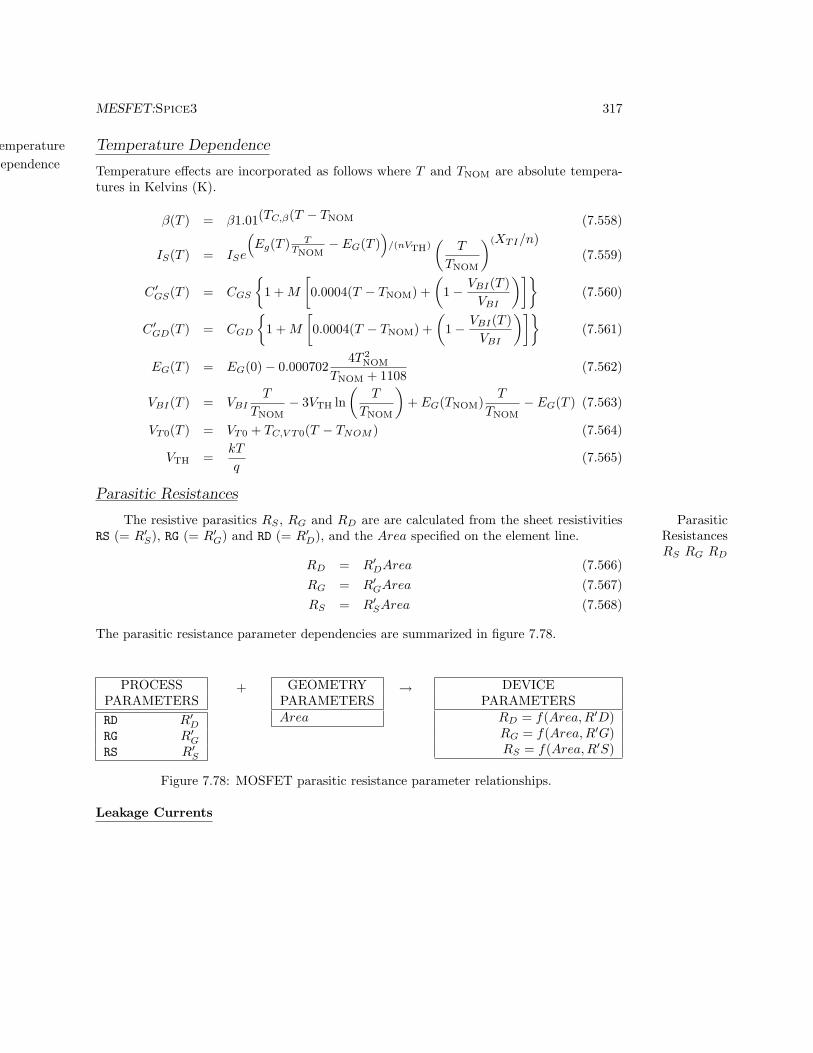
MESFET:Spice3 317
Temperature DependenceTemperatureDependence Temperature effects are incorporated as follows where T and TNOM are absolute tempera-
tures in Kelvins (K).
β(T ) = β1.01(TC,β(T − TNOM (7.558)
IS(T ) = ISe
(Eg(T ) T
TNOM− EG(T )
)/(nVTH)
(T
TNOM
)(XTI/n)(7.559)
C ′GS(T ) = CGS
1 + M
[0.0004(T − TNOM) +
(1− VBI(T )
VBI
)](7.560)
C ′GD(T ) = CGD
1 + M
[0.0004(T − TNOM) +
(1− VBI(T )
VBI
)](7.561)
EG(T ) = EG(0)− 0.0007024T 2
NOM
TNOM + 1108(7.562)
VBI(T ) = VBIT
TNOM− 3VTH ln
(T
TNOM
)+ EG(TNOM)
T
TNOM− EG(T ) (7.563)
VT0(T ) = VT0 + TC,V T0(T − TNOM ) (7.564)
VTH =kT
q(7.565)
Parasitic Resistances
The resistive parasitics RS , RG and RD are are calculated from the sheet resistivities ParasiticResistancesRS RG RD
RS (= R′S), RG (= R′G) and RD (= R′D), and the Area specified on the element line.
RD = R′DArea (7.566)RG = R′GArea (7.567)RS = R′SArea (7.568)
The parasitic resistance parameter dependencies are summarized in figure 7.78.
PROCESSPARAMETERSRD R′DRG R′GRS R′S
+ GEOMETRYPARAMETERSArea
→ DEVICEPARAMETERS
RD = f(Area, R′D)RG = f(Area, R′G)RS = f(Area, R′S)
Figure 7.78: MOSFET parasitic resistance parameter relationships.
Leakage Currents
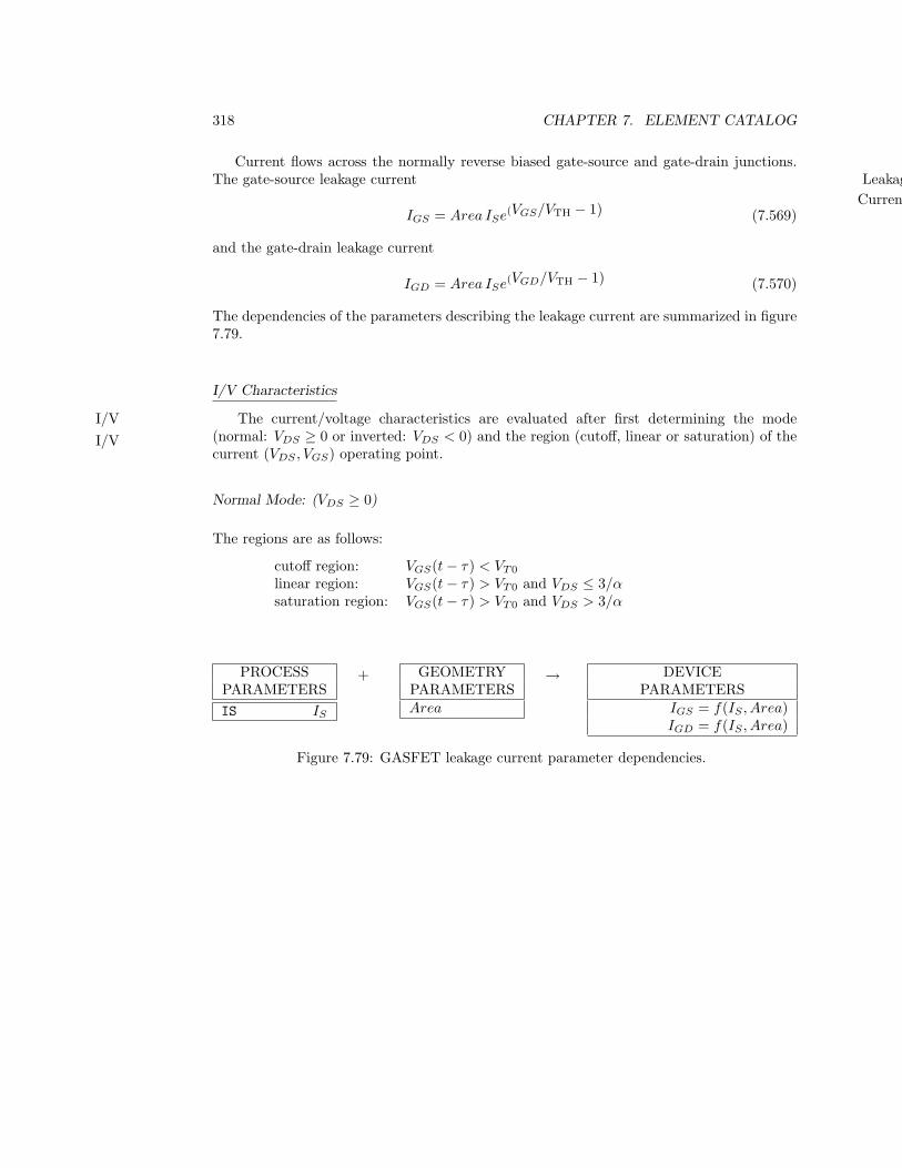
318 CHAPTER 7. ELEMENT CATALOG
Current flows across the normally reverse biased gate-source and gate-drain junctions.LeakageCurrents
The gate-source leakage current
IGS = Area ISe(VGS/VTH − 1) (7.569)
and the gate-drain leakage current
IGD = Area ISe(VGD/VTH − 1) (7.570)
The dependencies of the parameters describing the leakage current are summarized in figure7.79.
I/V Characteristics
The current/voltage characteristics are evaluated after first determining the modeI/VI/V (normal: VDS ≥ 0 or inverted: VDS < 0) and the region (cutoff, linear or saturation) of the
current (VDS , VGS) operating point.
Normal Mode: (VDS ≥ 0)
The regions are as follows:
cutoff region: VGS(t− τ) < VT0
linear region: VGS(t− τ) > VT0 and VDS ≤ 3/αsaturation region: VGS(t− τ) > VT0 and VDS > 3/α
PROCESSPARAMETERSIS IS
+ GEOMETRYPARAMETERSArea
→ DEVICEPARAMETERS
IGS = f(IS , Area)IGD = f(IS , Area)
Figure 7.79: GASFET leakage current parameter dependencies.

MESFET:Spice3 319
Then
IDS =
0 cutoff region
Area β (1 + λVDS) [VGS(t− τ)− VT0]2
1 + B[VGS(t− τ)− VT0]Ktanh linear and saturation
regions(7.571)
where
Ktanh =
1− (1− VDS
α3
)3 linear region
1 saturation regions(7.572)
is a taylor series approximation to the tanh function. Inverted Mode: (VDS < 0)
In the inverted mode the MOSFET I/V characteristics are evaluated as in the normal mode(7.571) but with the drain and source subscripts exchanged.
The relationships of the parameters describing the I/V characteristics of the model aresummarized in figure 7.80.
PROCESSPARAMETERSALPHA αB BBETA βLAMBDA λVTO VT0
+ GEOMETRYPARAMETERS
Area
→ DEVICEPARAMETERS
IDS =f(Area, α,B, β, λ, VT0)
Figure 7.80: LEVEL 2 (Raytheon model) I/V dependencies.
320 CHAPTER 7. ELEMENT CATALOG
CapacitancesCapacitances
The drain-source capacitanceCDS = AreaC ′DS (7.573)
The gate-source capacitance
CGS = Area
C ′GSF1F2
(1− Vnew
VBI
)− 12
+ C ′GDF3
(7.574)
The gate-source capacitance
CGD = Area
C ′GSF1F3
(1− Vnew
VBI
)− 12
+ C ′GDF2
(7.575)
where
F1 =12
1 +
Veff − VT0√(Ve − VT0)
2 + δ2
(7.576)
F2 =12
1 +
VGS − VGD√(VGS − VGD)2 + α−2
(7.577)
F3 =12
1− VGS − VGD√
(VGS − VGD)2 + α−2
(7.578)
Veff =12
VGS + VGD +
√(VGS − VGD)2 + α−2
(7.579)
(7.580)
Vnew =
A1 A1 < VMAX
VMAX A1 ≥ VMAX
(7.581)
andA1 =
12
[Ve + VT0 +
√(Ve + VT0)2 + δ2
](7.582)
In the model δ and VMAX are not settable by the user. Empirically they were determinedto be
VMAX = 0.5 delta = 0.2
The capacitance parameter dependencies are summarized in figure 7.81.

MESFET:Spice3 321
PROCESSPARAMETERSALPHA αCGD C ′GD
CGS C ′GS
CDS C ′DS
VBI VBI
VT0 VT0
M B
+ GEOMETRYPARAMETERS
Area
→ DEVICEPARAMETERS
CDS = f(Area, C ′DS)CGD = f(Area,C ′GD, α,
B, FC , VBI , VT0)CGS = f(Area, C ′GS , α,
B, FC , VBI , VT0)
Figure 7.81: Capacitance dependencies.
322 CHAPTER 7. ELEMENT CATALOG
ZAC Analysis
The AC analysis uses the model of figure ?? with the capacitor values evaluated at the DC
AC Analysis operating point with
gm =∂IDS
∂VGS(7.583)
andRDS =
∂IDS
∂VDS(7.584)
Noise Analysis
The MOSFET noise model accounts for thermal noise generated in the parasitic resis-Noise Analysistamces and shot and flicker noise generated in the drain source current generator. The rms(root-mean-square) values of thermal noise current generators shunting the four parasiticresistance RD, RG and RS areNoise Model
In,D =√
4kT/RD A/√
Hz (7.585)
In,G =√
4kT/RG A/√
Hz (7.586)
In,S =√
4kT/RS A/√
Hz (7.587)
Shot and flicker noise are modeled by a noise current generator in series with the drain-sourcecurrent generator. The rms value of this noise generator is
In,DS =√
I2SHOT,DS + I2
FLICKER,DS (7.588)
ISHOT,DS =
√4kTgm
23
A/√
Hz A/√
Hz (7.589)
IFLICKER,DS =
√KF IAF
DS
fA/√
Hz (7.590)
where the transconductancegm =
∂IDS
∂VGS(7.591)
is evaluated at the DC operating point and f is the analysis frequency.

323
324 CHAPTER 8. EXAMPLES
Chapter 8
Examples
8.1 Simple Differential Pair
The following circuit determines the dc operating point of a simple differential pair. In addi-tion, the ac small-signal response is computed over the frequency range 1Hz to 100MEGHz.
SIMPLE DIFFERENTIAL PAIRVCC 7 0 12VEE 8 0 -12VIN 1 0 AC 1RS1 1 2 1KRS2 6 0 1KQ1 3 2 4 MOD1Q2 5 6 4 MOD1RC1 7 3 10KRC2 7 5 10KRE 4 8 10K.MODEL MOD1 NPN BF=50 VAF=50 IS=1.E-12 RB=100 CJC=.5PF TF=.6NS.AC DEC 10 1 100MEG.END
8.2 MOS Output Characteristics
The following file computes the output characteristics of a MOSFET device over the range0-10V for VDS and 0-5V for VGS.
MOS OUTPUT CHARACTERISTICSVDS 3 0VGS 2 0M1 1 2 0 0 MOD1 L=4U W=6U AD=10P AS=10P.MODEL MOD1 NMOS VTO=-2 NSUB=1.0E15 UO=550* VIDS MEASURES ID, WE COULD HAVE USED VDS, BUT ID WOULD BE NEGATIVEVIDS 3 1.DC VDS 0 10 .5 VGS 0 5 1.END

8.2. MOS OUTPUT CHARACTERISTICS 325
326 CHAPTER 8. EXAMPLES
8.3 Simple RTL Inverter
The following file determines the dc transfer curve and the transient pulse response of asimple RTL inverter. The input is a pulse from 0 to 5 Volts with delay, rise, and fall timesof 2ns and a pulse width of 30ns. The transient interval is 0 to 100ns, with printing to bedone every nanosecond.
SIMPLE RTL INVERTERVCC 4 0 5VIN 1 0 PULSE 0 5 2NS 2NS 2NS 30NSRB 1 2 10KQ1 3 2 0 Q1RC 3 4 1K.MODEL Q1 NPN BF 20 RB 100 TF .1NS CJC 2PF.DC VIN 0 5 0.1.TRAN 1NS 100NS.END
8.4 Adder
The following file simulates a four-bit binary adder, using several subcircuits to describevarious pieces of the overall circuit.
ADDER - 4 BIT ALL-NAND-GATE BINARY ADDER*** SUBCIRCUIT DEFINITIONS.SUBCKT NAND 1 2 3 4* NODES: INPUT(2), OUTPUT, VCCQ1 9 5 1 QMODD1CLAMP 0 1 DMODQ2 9 5 2 QMODD2CLAMP 0 2 DMODRB 4 5 4KR1 4 6 1.6KQ3 6 9 8 QMODR2 8 0 1KRC 4 7 130Q4 7 6 10 QMODDVBEDROP 10 3 DMODQ5 3 8 0 QMOD.ENDS NAND.SUBCKT ONEBIT 1 2 3 4 5 6* NODES: INPUT(2), CARRY-IN, OUTPUT, CARRY-OUT, VCCX1 1 2 7 6 NANDX2 1 7 8 6 NANDX3 2 7 9 6 NANDX4 8 9 10 6 NANDX5 3 10 11 6 NANDX6 3 11 12 6 NANDX7 10 11 13 6 NANDX8 12 13 4 6 NANDX9 11 7 5 6 NAND.ENDS ONEBIT.SUBCKT TWOBIT 1 2 3 4 5 6 7 8 9* NODES: INPUT - BIT0(2) / BIT1(2), OUTPUT - BIT0 / BIT1,* CARRY-IN, CARRY-OUT, VCCX1 1 2 7 5 10 9 ONEBITX2 3 4 10 6 8 9 ONEBIT.ENDS TWOBIT.SUBCKT FOURBIT 1 2 3 4 5 6 7 8 9 10 11 12 13 14 15* NODES: INPUT - BIT0(2) / BIT1(2) / BIT2(2) / BIT3(2),* OUTPUT - BIT0 / BIT1 / BIT2 / BIT3, CARRY-IN, CARRY-OUT,VCCX1 1 2 3 4 9 10 13 16 15 TWOBITX2 5 6 7 8 11 12 16 14 15 TWOBIT.ENDS FOURBIT*** DEFINE NOMINAL CIRCUIT.MODEL DMOD D.MODEL QMOD NPN(BF=75 RB=100 CJE=1PF CJC=3PF)VCC 99 0 DC 5VVIN1A 1 0 PULSE(0 3 0 10NS 10NS 10NS 50NS)VIN1B 2 0 PULSE(0 3 0 10NS 10NS 20NS 100NS)VIN2A 3 0 PULSE(0 3 0 10NS 10NS 40NS 200NS)
VIN2B 4 0 PULSE(0 3 0 10NS 10NS 80NS 400NS)VIN3A 5 0 PULSE(0 3 0 10NS 10NS 160NS 800NS)VIN3B 6 0 PULSE(0 3 0 10NS 10NS 320NS 1600NS)VIN4A 7 0 PULSE(0 3 0 10NS 10NS 640NS 3200NS)VIN4B 8 0 PULSE(0 3 0 10NS 10NS 1280NS 6400NS)X1 1 2 3 4 5 6 7 8 9 10 11 12 0 13 99 FOURBITRBIT0 9 0 1KRBIT1 10 0 1KRBIT2 11 0 1KRBIT3 12 0 1KRCOUT 13 0 1K*** (FOR THOSE WITH MONEY (AND MEMORY) TO BURN).TRAN 1NS 6400NS.END\beginverbatim
\sectionTransmission-Line Inverter\labelex:trlinverterThe following file simulates a transmission-lineinverter. Two transmission-line elements are required sincetwo propagation modes are excited. In the case of a coaxialline, the first line (T1) models the inner conductor withrespect to the shield, and the second line (T2) models theshield with respect to the outside world.
\beginverbatimTRANSMISSION-LINE INVERTERV1 1 0 PULSE(0 1 0 0.1N)R1 1 2 50X1 2 0 0 4 TLINER2 4 0 50.SUBCKT TLINE 1 2 3 4T1 1 2 3 4 Z0=50 TD=1.5NST2 2 0 4 0 Z0=100 TD=1NS.ENDS TLINE.TRAN 0.1NS 20NS.END
8.5 Operational Amplifier
* MOSOPAMP.CIR
Basic Mosfet Op-amp
******
Set the ouput width to 80 columns
.WIDTH OUT = 80
VDD is the supply. The opamp has a single 5V supply.
VDD 1 0 DC 5V
Specify the MOSFETs and their connections
M1 5 5 1 1 PCH L=2.0U W=20U AD=136P AS=136PM2 6 5 1 1 PCH L=2.0U W=20U AD=136P AS=136PM3 5 3 4 0 NCH L=2.4U W=80U AD=136P AS=136PM4 6 2 4 0 NCH L=2.4U W=80U AD=136P AS=136PM5 7 6 1 1 PCH L=2.0U W=80U AD=136P AS=136PM6 1 7 8 0 NCH L=2.0U W=60U AD=136P AS=136P
The opamp has two inputs. Both are biased at 2.5V. The negative inputhas an AC signal. Note that the AC signal has a peak value of 1Vbut AC analysis is smaal signal so that this large AC value has nodoes not produce distortion. The output results of AC analysis areconveniently interpreted by setting the ACmagnitude of the sourceto 1.
VPOS 2 0 DC 2.5VNEG 3 0 DC 2.5 AC 1
Set the bias current sources.
I1 4 0 DC 0.1MAI2 7 0 DC 0.2MAI3 8 0 DC 1MA
.MODEL NCH NMOS LEVEL=2 VTO=0.71 GAMMA=0.29 CGSO=2.89E-10+ CGDO=2.89E-10 CJ=3.27E-4 MJ=0.4 TOX=225E-10 NSUB=3.5E16+ XJ=0.2E-6 LD=0 UO=411 UEXP=0 KF=6.5E-28 LAMBDA=0.02
.MODEL PCH PMOS LEVEL=2 VTO=-0.76 GAMMA=0.6 CGSO=3.35E-10+ CGDO=3.35E-10 CJ=4.75E-4 MJ=0.4 TOX=225E-10 NSUB=1.6E16+ XJ=0.2E-6 LD=0 UO=139 UEXP=0 KF=5E-30 LAMBDA=0.02
To determine operating point
.OP
To determine small signal analysis
.AC DEC 10 100 60MEG
Produce a table of the AC analysis results. Node 8 is the output.
.PRINT AC V(8)
Produce a plot of the AC analysis results.
.PLOT AC V(8)
Set initial conditions at several nodes to aid in convergencein determining the operating point.
.NODESET V(6)=3.5 V(7)=1.5 V(8)=2.5 V(4)=1.5
CURRENT THRU M1 AND M4 IS THE SAME = 0.05MA
.END
8.5.1 DC Analysis (.DC)
The DC analysis is specified by the .DC statement which is described on page 70.
8.5.2 Transfer characteristics.
8.5.3 Operating Point Analysis (.OP)
The operating point analysis is specified by the .OP statement which is described on page99.
8.5.4 AC Analysis (.AC)AC
The AC analysis is specified by the .AC statement which is described on page 67.
8.5.5 Distortion Analysis (.DISTO)
The distortion analysis is specified by the .DISTO statement which is described on page 74.
8.5.6 Monte Carlo Analysis (.MC)
The Monte Carlo analysis, specified by the .MC statement is only available with PSpice.The .MC statement is described on page 87.

8.5. OPERATIONAL AMPLIFIER 327
Descriptions of the basic algorithms of Spice.

328 CHAPTER 8. EXAMPLES

Bibliography
[1] McCalla
Descriptions of MOSFET models.
[2] P. Antognetti and G. Massobrio (editors), Semiconductor Device Modeling withSPICE, McGraw-Hill: New York, 1988.
[3] H. Shichman and D. A. Hodges, “Modeling and simulation of insulated-gate field-effecttransistor switching circuits,” IEEE Journal of Solid-State Circuits, Vol. 3, September1968, Page 285.
[4] J. E. Meyer, “MOS models and circuit simulation,” RCA Review, Vol 32., 1971.
[5] D. E. Ward and R. W. Dutton, “A channel-oriented model for MOS transistors ca-pacitances,” IEEE J. Solid-State Circuits, Vol. 13, 1978.
[6] S. Y. Oh, D. E. Ward and R. W. Dutton, “Transisent analysis of MOS transistors,”IEEE Trans. Electron Devices, Vol. 27, No. 8, 1980.
[7] A. Vladimirescu and S. Liu, The simulation of MOS transistor integrated circuits usingSPICE2, University of California, Berkeley, Memorandum No. M80/7, February 1980.
[8] K. Lee, M. Shur, T. Fjeldly and T. Ytterdal, Semiconductor Device Modeling forVLSI, Prentice Hall: Englewood Cliffs, New Jersey, 1993.
[9] B. J. Sheu, D.L. Scharfetter, P.-K. Ko, and M.-C. Jeng, “BSIM: Berkeley Short-Channel IGFET model for MOS transistors,” IEEE Journal of Solid-State Circuits,Vol 22, August 1987, pp. 558-566.
[10] J. R. Pierret, “ A MOS Parameter extraction program for the BSIM model, Universityof California, Berkeley, Memorandum No. M84/99, November 1984.
329

330 BIBLIOGRAPHY
Descriptions of MESFET models.
[11] W. R. Curtice, “A MESFET model for use in the design of GaAs integrated circuits,”IEEE Transactions on Microwave Theory and Techniques, Vol. 28, pp. 448-456, 1980.
[12] W.R. Curtice and M. Ettenberg, “A nonlinear GaAs FET model for use in the designof output circuits for power amplifiers,” IEEE Trans. on Microwave Theory and Tech.,Vol. MTT-33, Dec. 1985, pp. 1383-1393.
[13] T. Kacprzak and A. Materka, “Compact dc model of GaAs FET’s for large-signalcomputer calculation,” IEEE Journal of Solid-State Circuits, Vol. SC-18, April 1983,pp. 211-213.
[14] S.E. Sussman-Fort, “On the basic algorithms of SPICE with application to microwavecircuit simulation,” Presented at Nonlinear CAD and Modeling Workshop, IEEE In-ternational Microwave Symp. 1987
[15] S.E. Sussman-Fort, S. Narasimhan, and K. Mayaram, “A complete GaAs MESFETcomputer model for SPICE,” IEEE Trans. Microwave Theory and Tech., Vol. MTT-32, April 1984, pp. 471-473.
[16] S.E. Sussman-Fort, J.C. Hantgan, and F.L. Huang, “A SPICE model for enhancement-and depletion-mode GaAs FET’s,” IEEE Trans. Microwave Theory Tech., Vol. MTT-34, Nov. 1986, pp. 1115-1118.
[17] J.M. Golio, J.R. Hauser, and P.A. Blakey, “A large-signal GaAs MESFET modelimplemented on SPICE,” IEEE Circuits and Devices Magazine, Sep. 1985, pp. 21-30.
[18] J.M. Golio, P.A. Blakey, and R.O. Grondin, “A general CAD tool for large-signalGaAs MESFET circuit design,” IEEE MTT-S International Microwave SymposiumDigest, June 1985, pp. 417-420.
[19] Angelov:Zirath
[20] J.M. Golio, J.R. Hauser and P.A. Blakey “A large-signal GaAs MESFET model im-plemented on SPICE,” IEEE Circuits and Devices Magazine, Sept. 1985, pp. 21-30.
[21] J.M. Golio, P.A. Blakey, and R.O. Grondin, “A general CAD tool for large-signalGaAs MESFET circuit design,” IEEE MTT-S Digest, 417-420,.
[22] P.H. Ladbrooke, “Reverse modelling of GaAs MESFETs and HEMTs,” GEC Journalof Research, Vol. 6, 1988, pp. 1-9.
[23] H. Statz, P. Newman, I. .W. Smith, R. A. Pucel and H. A. Haus, “GaAs FET Deviceand Circuit Simulation in SPICE,” IEEE Transactions on Electron Devices, Vol. 34,pp 160–169, 1987.
[24] A. J. McCamant, G. D. McCormack, and D. H. Smith, “An improved GaAs MESFETModel for SPICE,” IEEE Transactions on Microwave Theory and Techniques, Vol. 38,pp. 822-824, June 1990.

BIBLIOGRAPHY 331
Descriptions of transformer model.
[25] D. C. Jiles and D. L. Atherton, “Theory of ferromagnetic hysteresis,” Journal ofMagnetism and Magnetic Materials, Vol. 61, 1986. pp. 48
[26] D. Divekar, “Comments no ‘GaAs FET devices and circuit simulation ni SPICE,’IEEE Trans. on Electron Devices, Vol. 34, December 1987, p. 2564.
[27] I.W. Smith, H. Statz, H.A. Haus, and R.A. Pucel, “On charge nonconservation inFETs,” IEEE Trans. on Electron Devices, Vol. 34, December 1987, pp.2565-2568.
Miscellaneous
[28] D. Knuth, The Art of Computer programming, Vol. 2.
[29] S. M. Sze, Physics of Semiconductor Devices, 2nd Edition, John Wiley and Sons: NewYork, 1981
[30] S. M. Sze, High-Speed Semiconductor Devices, John Wiley and Sons: New York, 1990.

332 BIBLIOGRAPHY

Appendix A
Statement Summary
333

334 APPENDIX A. STATEMENT SUMMARY

Appendix B
Element Summary
335

336 APPENDIX B. ELEMENT SUMMARY

Appendix C
Model Summary
337

338 APPENDIX C. MODEL SUMMARY
CAP Capacitor Model
Full description on page ??
Form
.MODEL modelName CAP( [ [keyword = value] ... ]

339
Coupled Inductor Model CORE
Full description on page ??
Form
.MODEL modelName CORE( [ [keyword = value] ... ]

340 APPENDIX C. MODEL SUMMARY
DIODE Diode Model
Full description on page 187
Form
.MODEL modelName DIODE( [ [keyword = value] ... ]

341
GaAs MESFET Model GASFET
Full description on page ??
Form
.MODEL modelName GASFET( [ [keyword = value] ... ]

342 APPENDIX C. MODEL SUMMARY
IMODEL Independent Current Source Model
Full description on page ??
Form
.MODEL modelName IMODEL( [ [keyword = value] ... ]

343
Inductor Model IND
Full description on page ??
Form
.MODEL modelName IND( [ [keyword = value] ... ]

344 APPENDIX C. MODEL SUMMARY
ISWITCH Current-Controlled Switch Model
Full description on page 307
Form
.MODEL modelName ISWITCH( [ [keyword = value] ... ]

345
Microstrip Right-Angle Bend LBEND
Full description on page ??
Form
.MODEL modelName LBEND( [ [keyword = value] ... ]

346 APPENDIX C. MODEL SUMMARY
MBEND Microstrip Mitered Right-Angle Bend Model
Full description on page ??
Form
.MODEL modelName MBEND( [ [keyword = value] ... ]

347
N-Channel JFET Model NJF
Full description on page 213
Form
.MODEL modelName MBEND( [ [keyword = value] ... ]

348 APPENDIX C. MODEL SUMMARY
NMOS N-Channel MOSFET Model
Full description on page 233
Form
.MODEL modelName NMOS( [ [keyword = value] ... ]

349
NPN BJT Model NPN
Full description on page 274
Form
.MODEL modelName NPN( [ [keyword = value] ... ]

350 APPENDIX C. MODEL SUMMARY
PMOS P-Channel MOSFET Model
Full description on page 233
Form
.MODEL modelName PMOS( [ [keyword = value] ... ]
Model parameters are the same as for the NMOS model. See page 348.

351
PNP BJT Model PNP
Full description on page 274
Form
.MODEL modelName PNP( [ [keyword = value] ... ]
Model parameters are the same as for the NPN model. See page 347.

352 APPENDIX C. MODEL SUMMARY
RES Resistor Model
Full description on page ??
Form
.MODEL modelName RES( [ [keyword = value] ... ]

353
Structure of Multiple Coupled Line (Y) Element Model STRUC
Full description on page ??
Form
.MODEL modelName STRUC( [ [keyword = value] ... ]

354 APPENDIX C. MODEL SUMMARY
TJUNC Microstrip T-Junction Model
Full description on page ??
Form
.MODEL modelName TJUNC( [ [keyword = value] ... ]

355
Lossy RC Transmission Line Model URC
Full description on page 292
Form
.MODEL modelName URC( [ [keyword = value] ... ]

356 APPENDIX C. MODEL SUMMARY
VMODEL Independent Voltage Source
Full description on page ??
Form
.MODEL modelName VMODEL( [ [keyword = value] ... ]

357
Voltage-Controlled Switch Model VSWITCH
Full description on page 287
Form
.MODEL modelName VSWITCH( [ [keyword = value] ... ]

358 APPENDIX C. MODEL SUMMARY
XJUNC Microstrip X-junction
Full description on page ??
Form
.MODEL modelName XJUNC( [ [keyword = value] ... ]

359
Microstrip Impedance Step Model ZSTEP
Full description on page ??
Form
.MODEL modelName ZSTEP( [ [keyword = value] ... ]

360 APPENDIX C. MODEL SUMMARY
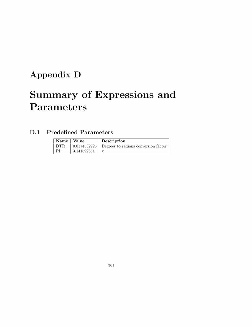
Appendix D
Summary of Expressions andParameters
D.1 Predefined Parameters
Name Value DescriptionDTR 0.0174532925 Degrees to radians conversion factorPI 3.141592654 π
361

362 APPENDIX D. SUMMARY OF EXPRESSIONS AND PARAMETERS
D.2 Algebraic Expressions
Arguments of trigonometric functions are in radians.
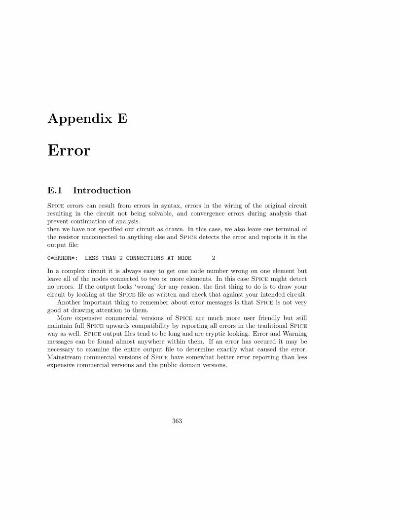
Appendix E
Error
E.1 Introduction
Spice errors can result from errors in syntax, errors in the wiring of the original circuitresulting in the circuit not being solvable, and convergence errors during analysis thatprevent continuation of analysis.then we have not specified our circuit as drawn. In this case, we also leave one terminal ofthe resistor unconnected to anything else and Spice detects the error and reports it in theoutput file:
0*ERROR*: LESS THAN 2 CONNECTIONS AT NODE 2
In a complex circuit it is always easy to get one node number wrong on one element butleave all of the nodes connected to two or more elements. In this case Spice might detectno errors. If the output looks ‘wrong’ for any reason, the first thing to do is to draw yourcircuit by looking at the Spice file as written and check that against your intended circuit.
Another important thing to remember about error messages is that Spice is not verygood at drawing attention to them.
More expensive commercial versions of Spice are much more user friendly but stillmaintain full Spice upwards compatibility by reporting all errors in the traditional Spiceway as well. Spice output files tend to be long and are cryptic looking. Error and Warningmessages can be found almost anywhere within them. If an error has occured it may benecessary to examine the entire output file to determine exactly what caused the error.Mainstream commercial versions of Spice have somewhat better error reporting than lessexpensive commercial versions and the public domain versions.
363

364 APPENDIX E. ERROR
In the following we list errors common to most versions of Spiceas they derive fromSpice2g6. Common errors for some of the commercial versions of Spice are also included.The errors are arranged in alphabetic order. Each commercial version of Spice supportsadditional elements that are particular to tha particular version but generally are selfex-planatory. For errors messages indicating a particular element the syntax of the elementdescribed in the element catalog chapter (chapter 7).
E.2 List of Errors
at least two numeric values requiredNot enough numeric values are provided. See the element form for the element.
cannot use LIST with DEC or OCT sweepsSee statement for correct form.
conflicting lengthWith a transmission line element either the time delay TD and the reference frequency Fare both specified or the time delay TD and the normalized electrical length NL are bothspecified. if the parameter pairs are specified then there are two possible electrical lengths.See the input forms of the T element on page 290.
conflicting specificationsWith an independent current source I or independent voltage sourceV element two or moretransient types are specified. See the allowable element line forms on page 203 for the Ielement and on page 297 for the V element.
contrary parametersSee page ?? for description of this element.
coupling coefficient out of range.The coupling coefficient for a K element must be between 0 amd 1.
digital files option not presentThe digital files (registered) option must be purchased separately. Spice version dependent.
ERROR -- . . . does not match nodes of . . .Commonly this is because the number of nodes of a subcircuit does not match the numberof nodes of a subcircuit call (X element).
ERROR: CPU Time limit exceededThe CPU time specified by the .OPTIONS parameter CPTIME, or its default, has been ex-ceeded.
E.2. LIST OF ERRORS 365
ERROR: less than 2 connections at node nnnnEvery node must have at least two connections or elese a node is left floating and the voltageat the node can not be determined. This may be either because the node is floating and thevoltage at the node is indeterminate or else because the numerical techniques used requireit.
ERROR: model . . . referenced by . . . is undefinedA model was referenced but the actual model was never specified via a .MODEL statement.
ERROR: Node is floatingThis is either because this is only one connection between this node or there is no DC pathfrom this node to ground as required in determining the DC voltage at the node.
ERROR: subcircuit . . . is undefinedA subcircuit was referenced but the actual subcircuit was never specified via a .SUBCKTstatement.
ERROR: transient analysis iterationsThe number of transient iterations specified by the .OPTIONS parameters ITL4 or ITL5, ortheir defaults, has been exceeded.
ERROR: voltage loopVoltage sources and/or elements such as inductors or transmission lines that are modeledusing controlled voltage sources, are arranged in a loop. This results in a modified nodealadmittance matrix that can not be solved.
ERROR: voltage source . . . which controls switch . . . is undefinedA voltage source was referenced but the actual element was never specified.
expand: parameter syntax error for . . .Error occurred during subcircuit expansion in handling parameters. With some version ofSpice parameters are supported. Parameters must be in the form Keyword = Value whereValue may be a numeric value or an expression. Either the Keyword is missing or is not analphanumeric quantity, or Value is missing or is neither a numeric quantity nor an expressionthat evaluates to a numeric quantity. The error is either on the X element line or on the.SUBCKT statement.
Expression evaluation error: function syntax errorError in expression evaluation or input prevents continuation.
Expression evaluation error: syntax errorError in expression evaluation or input prevents continuation.
Expression evaluation error: undefined parameterError in expression evaluation or input prevents continuation.
Error in expression.Error in expression evaluation or input prevents continuation.

366 APPENDIX E. ERROR
Expression syntax error.some versions of Spice support expressions. The expression is syntactically incorrect orother error that prevents evaluation of the expression.
extra fieldsExtra quantities on element line or statement that were not used.
function syntax error in expression.Error in expression evaluation or input prevents continuation.
incomplete rangeA range was indicated but is incomplete.
I(node) is not validTo specify currents a voltage source must be indicated. Specifying the current at a node ismeaningless.
incorrect number of parametersNot enough parameters specified for this element.
inductor: mutual coupling requires two (or more) inductorsA K element must comprise two or more inductors. This element is Spice version dependent.
inductor part of another CORE deviceAn inductor is specified as a component of two different K elements An inductor can onlybe part of one K element. This element is Spice version dependent.
inductor part of another K elementAn inductor is specified as a component of two different K elements An inductor can onlybe part of one K element. This element is Spice version dependent.
inductor part of another mutual coupling deviceAn inductor is specified as a component of two different K elements An inductor can onlybe part of one K element. This element is Spice version dependent.
inductor part of this K deviceA K element contains two inductors of the same name. An inductor can only be specifiedonce in a K element inductor list. This element is Spice version dependent.
invalid .WIDTH cardThe parameters on the .WIDTH card are incorrectly specified or a parameter is not supportedby this version of Spice.
invalid analysis typeAnalysis type specified on a .FOUR .TF .NOISE .SENS .MC .PLOT .PRINT .PROBEstatement is incorrect. Supported analysis types include AC, DC, TRAN and NOISE al-though this list is Spice version dependent. See the full description of the allowable analysistypes for the statement.
E.2. LIST OF ERRORS 367
invalid cardThe statement may be spelled incorrectly or this version of Spice does not recognize thisstatement.
invalid deviceThe first letter of an element card indicates the particular device being referred to. Not allversions of Spice support the same set of elements and here an non-supported element isbeing invoked.
invalid device in subcircuitGenerally any element may be used with a subcircuit. (between .SUBCKT and .ENDS. Someversions of Spice support special elements or forms of elements that can only be used atthe top level circuit. See the description of the element.
invalid dimensionThe degree (dimension or order) of a polynomial must be more than 0 and less than themax polynomial order supported by the current version of Spice.
invalid functionSome commercial versions of Spice support function evaluations. An unsupported functionis being used.
invalid incrementUsually caused by specifying an increment of zero on a .DC statement
invalid node number in .SUBCKT statementThe invalid node number was specified in .SUBCKT statement. This is usually because theground node (either 0 or, in some versions of Spice “GND”) was specified in the list of nodesin the .SUBCKT statement.
invalid numberDue to a number being of the wrong sign or too small or zero where this is not valid. Possiblyan integer was expected and a floating point number was supplied.
invalid optionThe value of the parameter is invalid.
invalid outside of .SUBCKT.ENDS is used out of context and does not terminate a subcircuit.
invalid parameterInvalid parameter on element line. Probably misspelled or not supported by this version ofSpice.
invalid parameter in modelEither the parameter is misspelled ot it is not supported by this version of Spice.
invalid port name for transmission linePort name in output list is either missing or invalid.
368 APPENDIX E. ERROR
invalid print intervalSee the analysis statement for the requirements on specifying the output reporting interval.
invalid run numberA negative number of runs was specified in a Monte Carlo analysis.
invalid specificationError in specifying element. See the form for this element.
invalid step sizeStep size must be positive.
invalid sweep typeSweep type not supported by this version of Spice or sweep type incorrectly specified.
invalid valueDue to a value being of the wrong sign or too small or zero where this is not valid. Possiblyan integer was expected and a floating point number was supplied.
last PWL pair incompleteThe piecewise linear characteristic of an I or V element must be specified in time,value pairs.
list of runsNo runs were specified in a Monte Carlo analysis
missing .ENDS in .SUBCKTA subcircuit must end with a .ENDS statement. This was missing.
missing analysis typeAnalysis type must be specified in a .FOUR .TF .NOISE .SENS .MC .PLOT .PRINT.PROBE statement but is missing.
missing component valueComponent value for R L or C element missing
missing control nodeA control node is missing for an E element.
missing controlling sourceThe name of a controlling voltage source is missing for a G element.
missing device or nodedevice or node expected but missing.
missing dimensionThe degree (dimension or order) of a polynomial not specified. The degree of a polynomialshould be specified in the form “POLY(n)” or “POLY n ”.
missing file nameFile name expected in a .INCL but missing.
E.2. LIST OF ERRORS 369
missing frequencyFrequency missing on a .FOUR card.
missing gainThe gain must be specified for an E or F element.
missing inductorIn reading K element line expected to read in the name of an inductor but it was missing.
missing INOISE or ONOISE.NOISE statement and either INOISE or ONOISE parameters required or illegal parameter.
missing modelModel Name expected on element line but was missing
missing model nameModel Name expected on element line but was missing
missing nameSubcircuit name expected on .SUBCKT (or similar) statement but not found.
missing nodeA node number expected but not provided. Possibly not enough nodes specified. See theform for this element in the element catalog (chapter 7.
missing node listNo nodes are specified.
missing or invalid model name or typeEither the model name is missing or it is not a valid type for this element.
missing or invalid valueDue to a value not being supplied where it is expected, being of the wrong sign or too smallor zero where this is not valid. Possibly an integer was expected and a floating point numberwas supplied.
missing output variablesNo output variables specified for a .FOUR .TF .NOISE .SENS .MC .PLOT .PRINT .PROBEstatement.
missing parameterParameter expected but not found.
missing pnrIn a .AS statement the port number is missing.
missing polynomialThe POLY keyword was specified but no polynomial coefficients were found.
370 APPENDIX E. ERROR
missing run countThe number of Monte Carlo runs is incorrectly specified.
missing second port in S(pnr1,pnr2)There must be a second port in a .AS output specification.
missing second node in V(node1,node2)In this syntax two nodes must be specified.
missing seedA random number seed was expected for this element but it was missing
missing sourceName of source expected but it was not supplied.
missing subcircuit nameSubcircuit name expected on .SUBCKT statement but not found.
missing sweep typeSweep type not specified for .AC analysis.
missing transconductanceThe transconductance must be specified for a G element.
missing transresistanceThe transresistance must be specified for an H element.
missing valueValue (or expression) expected but not found. Either a non-numeric quantity (i.e. not anumber) is in a location where a numeric value value is expected or a quantity is missing.If an expression was specified it was either incorrectly delimited or its evaluation is notsupported by this version of Spice.
must be >= 1An positive integer value was expected upon input but the value was not 1 or more.
must be a two terminal deviceTo specify a current a two terminal device must be indicated. More elements with morethan three terminals the edge current cannot be uniquely identified by specifying the nodes.
must be a voltage source nameName of voltage source expected on element line but not supplied A voltage source namemust begin with V.
must be an inductorIn reading K element line expected to read in the name of an inductor but the name didnot begin with ’L’

E.2. LIST OF ERRORS 371
must be I or VIn a .AC, .FOUR .TF .SENS .MC .PLOT .PRINT .PROBE statement. Only I or V can bespecified. Something else is in output list. Generally this is because only I or V elementscan be swept.
must be independent source (I or V)An element was specified but it was not an I or V element.
must be monotonically increasing or decreasingQuantities in list must be monotonically increasing or decreasing.
must be SThe keyword “S” expected.
must be VA list of voltage sources is required but either a numeric value was provided an elementother than a voltage source specified. (The voltage sources in list of must begin with V.)In the case of a polynomial specification the number of controlling voltage sources must beequal to the polynomial degree previously specified on the element line. Either not enoughvoltage sources are specified or a non-voltage source is specified.
name on .ENDS does not match .SUBCKTAn optional name may be included on a .ENDS statement. If specified it must match thename specified on the matching .SUBCKT statement.
nesting level exceededThe number of files that can be included using .INCL is limited. The limit is Spice versionspecific but is typically around 5.
node’s voltage already setTwo attempts have been made to set the initial voltage at a node. The initial value may bespecified using either a .NODESET statement or using the initial condition IC parameter onsome elements.
not a valid parameter for model typeparameter not recognized for this model.
not uniqueSome versions of Spiceallow abbreviated forms of statements. The minimum allowableabbreviation must be unique. The abbreviation used in the netlist is not unique and is anabbreviation of two or more statements.
only .AC .DC and .TRAN validThe type of analysis in a Monte Carlo run must be either .DC
, .AC or .TRAN.

372 APPENDIX E. ERROR
only .MODEL valid in subcircuit.MODEL is the only statement allowed within a subcircuit description (between /SUBCKT and.ENDS.
only one .TEMP and .DC TEMP allowedOne .TEMP statement and one .DC TEMP statement allowed but not both. This is Spiceversion dependent.
Parameter syntax errorWith some version of Spice parameters are supported. The “PARAMS:” keyword indicatesthat parameters are to be specified in the form Keyword = Value where Value may be anumeric value or an expression. Either the Keyword is missing or is not an alphanumericquantity, or Value is missing or is neither a numeric quantity nor an expression that evaluatesto a numeric quantity..
PNR already definedThe port number can only be defined once.
PNR missing or invalidThe port number was either missing or not correctly specified.
run countThe number of Monte Carlo runs is incorrectly specified.
run count must be > 1The number of Monte Carlo runs is incorrectly specified.
syntax error.Input is in error. Often due to an non-numeric value in input where a non-numeric valueexpected or vice-versa.
syntax error in expression.Error in expression evaluation or input prevents continuation.
TD or F must be specifiedWith a transmission line element either the time delay TD or reference frequency F must bespecified. See the T element on page 290.
temperatureA 0 K (Kelvin) temperature is not valid. The usual problem is that a 0 Celsius tempera-ture was specified but a temperature specified by a .temp statement must be an absolutetemperature (in Kelvin)Q
time must be increasingIn specifying the transient behavior of an I or V element times must be increasing.
time must not be negativeIn specifying the transient behavior of an I or V element a negative time was specified.

E.2. LIST OF ERRORS 373
too many coefficientsThe number of polynomial coefficients specified exceeds that supported in this version ofSpice.
too many inductorsThere is a limit on the number of inductors per K element. This limit has been exceeded.
too many tolerancesThe number of tolerances that may be specified is limited. This limit is Spice versiondependent.
TooManyToo many parameters, values or nodes on element line or .SUBCKT statement.
unable to open fileFile specified in a .INCL or .LIB does not exist in the current directory or default directories.
undefined parameterAn unsupported parameter keyword specified. Either this version of Spice does not supportthis parameter for this element or statement or the parameter is misspelled.
unknown parameterA parameter was used on an element line or in a .MODEL statement which was not recognized.Either this version of Spice does not support this parameter or the parameter is misspelled.
value may not be 0A non-zero value expected.
voltage source nameName of voltage source expected on element line but not supplied
WIDTH must be 80 or 132A Spice supports two output log formats that are either 80 columns or 132 columns wide.A width other than 80 or 132 was specified.
Z0 must be specifiedWith a transmission line element the Z0 parameter must always be input using the syntaxZ0=CharacteristicImpedance.

374 APPENDIX E. ERROR

Glossary
375

376 GLOSSARY

Appendix F
Reference Card
377