sphv-c series 200w discrete bidirectional tvs diode rohs green · sphv-c series 200w discrete...
TRANSCRIPT

TVS Diode Array (SPA ® Diodes)General Purpose ESD Protection - SPHV-C Series
© 2019 Littelfuse, Inc.Specifications are subject to change without notice.
Revised: 09/24/19
Description
Applications
The Bidirectional SPHV-C series is designed for use in portable applications, LED lighting modules, automotive applications, and low speed I/Os. It will protect sensitive equipment from damage due to electrostatic discharge (ESD) and other overvoltage transients.
The SPHV-C series can safely absorb repetitive ESD strikes above the maximum level of the IEC 61000-4-2 international standard (Level 4, ±8kV contact discharge) without performance degradation and safely dissipate up to 8A (SPHV12-C) of induced surge current (IEC 61000-4-5, 2nd Edition tP=8/20μs) with very low clamping voltages.
Features
SPHV-C Series 200W Discrete Bidirectional TVS Diode
Pinout
Functional Block Diagram
Life Support Note:
Not Intended for Use in Life Support or Life Saving Applications
The products shown herein are not designed for use in life sustaining or life saving applications unless otherwise expressly indicated.
1
2
1 2
• LED Lighting Modules
• Portable Instrumentation
• General Purpose I/O
• Mobile & Handhelds
• RS232 / RS485
• CAN and LIN Bus
RoHS Pb GREEN
• ESD, IEC 61000-4-2,
±30kV contact, ±30kV air
• EFT, IEC 61000-4-4, 40A
(5/50ns)
• Lightning, IEC 61000-4-5 2nd edition, 8A (tP=8/20μs, SPHV12-C)
• Low clamping voltage
• Low leakage current
• Small SOD882 packaging helps save board space
• Lead-free and RoHS compliant
• AEC-Q101 qualified(SOD882 ETG series)
• Side exposed leadframe helps to verify solderability (SPHVxx-KTG-C series)
Additional Information
Datasheet SamplesResources

TVS Diode Array (SPA ® Diodes)General Purpose ESD Protection - SPHV-C Series
© 2019 Littelfuse, Inc.Specifications are subject to change without notice.
Revised: 09/24/19
CAUTION: Stresses above those listed in “Absolute Maximum Ratings” may cause permanent damage to the device. This is a stress only rating and operation of the device at these or any other conditions above those indicated in the operational sections of this specification is not implied.
Absolute Maximum Ratings
Symbol Parameter Value Units
Ppk Peak Pulse Power (tp=8/20μs) 200 W
TOP Operating Temperature -40 to 125 °C
TSTOR Storage Temperature -55 to 150 °C
Thermal Information
Parameter Rating Units
Storage Temperature Range -55 to 150 °C
Maximum Junction Temperature 150 °C
Maximum Lead Temperature (Soldering 20-40s) 260 °C
SPHV12-C Electrical Characteristics (TOP=25ºC)
Parameter Symbol Test Conditions Min Typ Max Units
Reverse Standoff Voltage VRWM IR≤1μA 12.0 V
Reverse Breakdown Voltage VBR IR=1mA 13.3 V
Leakage Current ILEAK VR=12V 1.0 μA
Clamp Voltage1 VC
IPP=1A, tp=8/20µs, Fwd 19.0 V
IPP=8A, tP=8/20μs, Fwd 25.0 V
Dynamic Resistance2 RDYN TLP, tp=100ns, I/O to GND 0.48 Ω
Peak Pulse Current Ipp tp=8/20µs 8.0 A
ESD Withstand Voltage1 VESD
IEC61000-4-2 (Contact Discharge) ±30 kV
IEC61000-4-2 (Air Discharge) ±30 kV
Diode Capacitance1 CD-GND Reverse Bias=0V, f=1MHz 30 pF
SPHV15-C Electrical Characteristics (TOP=25ºC)
Parameter Symbol Test Conditions Min Typ Max Units
Reverse Standoff Voltage VRWM IR≤1μA 15.0 V
Reverse Breakdown Voltage VBR IR=1mA 16.7 V
Leakage Current ILEAK VR=15V 1.0 μA
Clamp Voltage1 VC
IPP=1A, tp=8/20µs, Fwd 22.0 V
IPP=5A, tp=8/20µs, Fwd 30.0 V
Dynamic Resistance2 RDYN TLP, tp=100ns, I/O to GND 0.43 Ω
Peak Pulse Current Ipp tp=8/20µs 5.0 A
ESD Withstand Voltage1 VESD
IEC61000-4-2 (Contact Discharge) ±30 kV
IEC61000-4-2 (Air Discharge) ±30 kV
Diode Capacitance1 CI/O-GND Reverse Bias=0V, f=1MHz 24 pF
Note:1. Parameter is guaranteed by design and/or device characterization. 2. Transmission Line Pulse (TLP) with 100ns width and 200ps rise time.
Note:1. Parameter is guaranteed by design and/or device characterization. 2. Transmission Line Pulse (TLP) with 100ns width and 200ps rise time.
TVS Diode Array (SPA ® Diodes)General Purpose ESD Protection - SPHV-C Series
© 2019 Littelfuse, Inc.Specifications are subject to change without notice.
Revised: 09/24/19
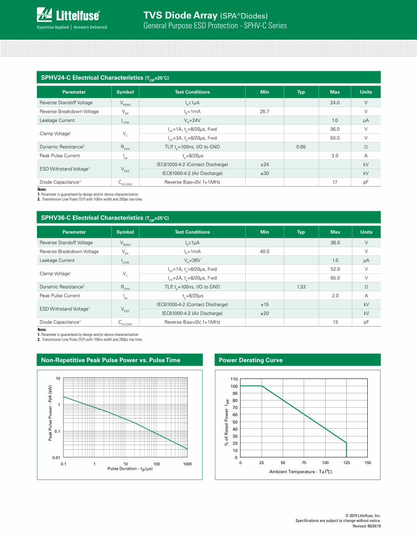
SPHV24-C Electrical Characteristics (TOP=25ºC)
Parameter Symbol Test Conditions Min Typ Max Units
Reverse Standoff Voltage VRWM IR≤1μA 24.0 V
Reverse Breakdown Voltage VBR IR=1mA 26.7 V
Leakage Current ILEAK VR=24V 1.0 μA
Clamp Voltage1 VC
IPP=1A, tp=8/20µs, Fwd 36.0 V
IPP=3A, tp=8/20µs, Fwd 50.0 V
Dynamic Resistance2 RDYN TLP, tp=100ns, I/O to GND 0.65 Ω
Peak Pulse Current Ipp tp=8/20µs 3.0 A
ESD Withstand Voltage1 VESD
IEC61000-4-2 (Contact Discharge) ±24 kV
IEC61000-4-2 (Air Discharge) ±30 kV
Diode Capacitance1 CI/O-GND Reverse Bias=0V, f=1MHz 17 pF
SPHV36-C Electrical Characteristics (TOP=25ºC)
Parameter Symbol Test Conditions Min Typ Max Units
Reverse Standoff Voltage VRWM IR≤1μA 36.0 V
Reverse Breakdown Voltage VBR IR=1mA 40.0 V
Leakage Current ILEAK VR=36V 1.0 μA
Clamp Voltage1 VC
IPP=1A, tp=8/20µs, Fwd 52.0 V
IPP=2A, tp=8/20µs, Fwd 65.0 V
Dynamic Resistance2 RDYN TLP, tp=100ns, I/O to GND 1.33 Ω
Peak Pulse Current Ipp tp=8/20µs 2.0 A
ESD Withstand Voltage1 VESD
IEC61000-4-2 (Contact Discharge) ±15 kV
IEC61000-4-2 (Air Discharge) ±20 kV
Diode Capacitance1 CI/O-GND Reverse Bias=0V, f=1MHz 13 pF
Non-Repetitive Peak Pulse Power vs. Pulse Time
Pulse Duration - tp (µs)
Pea
k Pu
lse
Po
wer
- P
pk
(kW
)
0.01
0.1
1
10
0.1 1 10 100 1000
Note:1. Parameter is guaranteed by design and/or device characterization. 2. Transmission Line Pulse (TLP) with 100ns width and 200ps rise time.
Note:1. Parameter is guaranteed by design and/or device characterization. 2. Transmission Line Pulse (TLP) with 100ns width and 200ps rise time.
Power Derating Curve
0
10
20
30
40
50
60
70
80
90
100
110
0 25 50 75 100 125 150
Ambient Temperature - TA (oC)
% o
f R
ated
Po
wer
IP
P

TVS Diode Array (SPA ® Diodes)General Purpose ESD Protection - SPHV-C Series
© 2019 Littelfuse, Inc.Specifications are subject to change without notice.
Revised: 09/24/19
8/20µs Pulse Waveform
0%
10%
20%
30%
40%
50%
60%
70%
80%
90%
100%
110%
0.0 5.0 10.0 15.0 20.0 25.0 30.0
Time (μs)
Per
cen
t o
f I P
P
0
2
4
6
8
10
12
14
16
18
20
0 5 10 15 20 25 30
TLP Voltage (V)
TLP
Curr
ent (
A)
SPHV12-C Transmission Line Pulsing(TLP) Plot
0
2
4
6
8
10
12
14
16
18
20
0 5 10 15 20 25 30 35
TLP Voltage (V)
TLP
Curr
ent (
A)
SPHV15-C Transmission Line Pulsing(TLP) Plot
0
2
4
6
8
10
12
14
16
18
20
0 5 10 15 20 25 30 35 40 45 50 55
TLP Voltage (V)
TLP
Curr
ent (
A)
SPHV24-C Transmission Line Pulsing(TLP) Plot
SPHV36-C Transmission Line Pulsing(TLP) Plot
0
2
4
6
8
10
12
14
16
0 10 20 30 40 50 60 70 80 90 100
TLP Voltage (V)
TLP
Curr
ent (
A)

TVS Diode Array (SPA ® Diodes)General Purpose ESD Protection - SPHV-C Series
© 2019 Littelfuse, Inc.Specifications are subject to change without notice.
Revised: 09/24/19
Time
Tem
pera
ture
TP
TL
TS(max)
TS(min)
25
tP
t L
tS
time to peak temperature
PreheatPreheat
Ramp-upRamp-up
Ramp-downRamp-dow
Critical ZoneTL to TP
Critical ZoneTL to TP
Soldering Parameters
Ordering InformationProduct Characteristics
Lead Plating Pre-Plated Frame
Lead Material Copper Alloy
Lead Coplanarity 0.0004 inches (0.102mm)
Substitute Material Silicon
Body Material Molded Epoxy, rated UL 94 V-0Notes : 1. All dimensions are in millimeters2. Dimensions include solder plating.3. Dimensions are exclusive of mold flash & metal burr.4. Blo is facing up for mold and facing down for trim/form, i.e. reverse trim/form.5. Package surface matte finish VDI 11-13.
Part Number Package Marking Min. Order Qty.
SPHV12-01ETG-C
SOD882
B2
10000SPHV15-01ETG-C B5
SPHV24-01ETG-C B4
SPHV36-01ETG-C B6
SPHV12-01KTG-CSOD882 with side exposed
leadframe
B2
10000SPHV15-01KTG-C B5
SPHV24-01KTG-C B4
SPHV36-01KTG-C B6
Part Numbering SystemPart Marking System
SPHV ** 01 T G
VoltageNumber ofChannels
PackageT= Tape & Reel
G= Green
–
TVS Diode Arrays(SPA® Diodes )
E: SOD882
x – C
Bidirectional
K: SOD882 with side exposed leadframe
B*
2: SPHV12-C5: SPHV15-C4: SPHV24-C6: SPHV36-C
1 2
Reflow Condition Pb – Free assembly
Pre Heat
- Temperature Min (Ts(min)) 150°C
- Temperature Max (Ts(max)) 200°C
- Time (min to max) (ts) 60 – 180 secs
Average ramp up rate (Liquidus) Temp (TL) to peak 3°C/second max
TS(max) to TL - Ramp-up Rate 3°C/second max
Reflow- Temperature (TL) (Liquidus) 217°C
- Temperature (tL) 60 – 150 seconds
Peak Temperature (TP) 260+0/-5 °C
Time within 5°C of actual peak Temperature (tp) 20 – 40 seconds
Ramp-down Rate 6°C/second max
Time 25°C to peak Temperature (TP) 8 minutes Max.
Do not exceed 260°C

TVS Diode Array (SPA ® Diodes)General Purpose ESD Protection - SPHV-C Series
© 2019 Littelfuse, Inc.Specifications are subject to change without notice.
Revised: 09/24/19
Embossed Carrier Tape & Reel Specification
Feeding DirectionTop mark and pin 1 direction in Tape and Reel
BX
1
2
Package Dimensions — SOD882(SPHVxx-01ETG-C)
Recommended soldering pad layout (unit:mm)
0.30mm 0.45mm
1.20mm
0.70
mm
Symbol
Package SOD882
JEDEC MO-236
Millimeters Inches
Min Typ Max Min Typ Max
A 0.90 1.00 1.10 0.037 0.039 0.041
B 0.50 0.60 0.70 0.022 0.024 0.026
C 0.40 0.50 0.60 0.016 0.020 0.024
D 0.45 0.018
E 0.20 0.25 0.35 0.008 0.010 0.012
F 0.45 0.50 0.55 0.018 0.020 0.022
Symbol Millimeters
A 0.70+/-0.045
B 1.10+/-0.045
C 0.65+/-0.045
d 1.55+/-0.10
E 1.75+/-0.05
F 3.50+/-0.05
P 2.00+/-0.10
P0 4.00+/-0.10
P1 2.00+/-0.10
W 8.00 + 0.30 -0.10
Package Dimensions — SOD882 with side exposed leadframe(SPHVxx-01KTG-C)A
B
C
I
E
G
F
H
D
d
c
a
b
Side Exposed Leadframe
Side View
Top View
Bottom View
0.28
0.14
0.075
Recommended soldering pad layout (unit:mm)
0.30mm 0.45mm
1.20mm
0.70
mm
*Some ETG packaging will look like KTG packaging due to the differing package construction between various suppliers.
Symbol
Package SOD882 with side exposed leadframe
JEDEC MO-236
Millimeters Inches
Min Typ Max Min Typ Max
A 0.90 1.00 1.10 0.037 0.039 0.043
B 0.50 0.60 0.70 0.020 0.024 0.028
C 0.90 1.00 1.10 0.037 0.039 0.043
D 0.55 0.65 0.75 0.022 0.026 0.030
E 0.40 0.50 0.60 0.016 0.020 0.024
F 0.50 0.60 0.70 0.020 0.024 0.028
G 0.20 0.25 0.30 0.008 0.010 0.012
H 0.40 0.50 0.60 0.016 0.020 0.024
I 0.05 max 0.002 max
a - 0.14 - - 0.006 -
b - 0.05 - - 0.002 -
c - 0.075 - - 0.003 -
d - 0.10 - - 0.004 -
Disclaimer Notice - Information furnished is believed to be accurate and reliable. However, users should independently evaluate the suitability of and test each product selected for their own applications. Littelfuse products are not designed for, and may not be used in, all applications. Read complete Disclaimer Notice at http://www.littelfuse.com/disclaimer-electronics.