spherically shaped micro-structured antireflective surfaces
TRANSCRIPT
Spherically shaped micro-structured
antireflective surfaces
R. Bouffaron1,2
, L. Escoubas1,2,
*, V. Brissonneau1,4
, J. J. Simon1,2
, G. Berginc4, Ph.
Torchio1,2
, F. Flory1,3
and Ph. Masclet5
1 Aix-Marseille University, IM2NP, France 2 CNRS, IM2NP UMR 6242 (Marseille – Toulon), France
3 Ecole Centrale Marseille, France 4 Thalès Optronique S.A., Guyancourt, France
5 Délégation Générale pour l’Armement (DGA), Paris, France
Abstract: An antireflecting micro-structured interface, working in the
resonance domain, and made from a bi-periodic array of semi-spherical
hollowing-out in a silicon substrate is presented. Its parameters such as
sphere radius and position of sphere centers from the surface are optimized
numerically. A simple and robust process is described allowing such kind
of antireflective surfaces to be fabricated for the infrared range. Spectral
and angular reflectance measurement demonstrates the efficiency of the
antireflective micro-structured interface which can easily be adapted for the
visible range and for photovoltaic applications by a simple homothetic
modification of the micro-structure typical dimensions.
©2009 Optical Society of America
OCIS codes: (050.5298) Photonic crystals; (050.5745) Resonance domain; (050.6624)
Subwavelength structures; (310.1210) Antireflection coatings
References and links
1. A. Gombert, B. Blasi, C. Buhler, P. Nitz, J. Mick, W. Hoßfeld, and M. Niggemann, “Some application cases and
related manufacturing techniques for optically functional microstructures on large areas,” Opt. Eng. 43(11),
2525–2533 (2004).
2. H. A. Macleod, Thin film optical filters (Institute of Physics Publishing, London, 1986).
3. J. A. Dobrowolski, D. Poitras, P. Ma, H. Vakil, and M. Acree, “Toward perfect antireflection coatings:
numerical investigation,” Appl. Opt. 41(16), 3075–3083 (2002).
4. P. B. Clapham, and M. C. Hutley, “Reduction of Lens Reflexion by the “Moth Eye” Principle,” Nature
244(5414), 281–282 (1973).
5. Y. Zhao, J. Wang, and G. Mao, “Colloidal subwavelength nanostructures for antireflection optical coatings,”
Opt. Lett. 29, 993–1009 (1982).
6. H. Sai, H. Fujii, K. Arafune, Y. Ohshita, M. Yamaguchi, Y. Kanamori, and H. Yugami, “Antireflective
subwavelength structures on crystalline Si fabricated directly formed anodic porous masks,” Opt. Lett. 29, 993–
1009 (1982).
7. H. Xu, N. Lu, D. Qi, J. Hao, L. Gao, B. Zhang, and L. Chi, “Biomimetic antireflective Si nanopillar arrays,”
Small 4(11), 1972–1975 (2008).
8. Z. Yu, H. Gao, W. Wu, H. Ge, and S. Y. Chou, “Fabrication of large area subwavelength antireflection
structures on Si using trilayer resist nanoimprint lithography and liftoff,” J. Vac. Sci. Technol. B 21(6), 2874–
2877 (2003).
9. Y. C. Chang, G. H. Mei, T. W. Chang, T. J. Wang, D. Z. Lin, and C. K. Lee, “Design and fabrication of a
nanostructured surface combining antireflective and enhanced-hydrophobic effects,” Nanotechnology 18(28),
285303 (2007).
10. M. Born, and E. Wolf, Principles of Optics (Pergamon, London, 1980), 705 – 708.
11. E. B. Grann, M. G. Varga, and D. A. Pommet, “Optimal design for antireflective tapered two-dimensional
subwavelength grating structures,” J. Opt. Soc. Am. A 12(2), 333–339 (1995).
12. R. Bouffaron, L. Escoubas, J. J. Simon, P. Torchio, F. Flory, G. Berginc, and P. Masclet, “Enhanced
antireflecting properties of micro-structured top-flat pyramids,” Opt. Express 16(23), 19304–19309 (2008).
13. L. Escoubas, J. J. Simon, M. Loli, G. Berginc, F. Flory, and H. Giovannini, “An antireflective silicon grating
working in the resonance domain for the near infrared spectral region,” Opt. Commun. 226(1-6), 81–88 (2003).
#115762 - $15.00 USD Received 17 Aug 2009; revised 16 Sep 2009; accepted 8 Oct 2009; published 11 Nov 2009
(C) 2009 OSA 23 November 2009 / Vol. 17, No. 24 / OPTICS EXPRESS 21590
14. K. Busch, and S. John, “Liquid-Crystal Photonic-Band-Gap Materials: The Tunable Electromagnetic Vacuum,”
Phys. Rev. Lett. 83(5), 967–970 (1999).
1. Introduction
Antireflective surfaces working for broad wavelength ranges and large incidence angles are
very useful for a wide variety of applications: to enhance the efficiency of photovoltaic cells
[1], to increase the sensitivity of photodetectors, to improve the performance of light emitting
diodes, etc. Basic conventional antireflection coatings generally consist of a single layer,
which has a refractive index equals to the square root of the product of the adjacent materials
ones [2]. This kind of antireflective layer allows reducing the reflectance until zero, but only
for the specific wavelength for which the optical thickness of the films is quaterwave (called
“centering wavelength”). It is well known that such single layer antireflection coatings do not
operate well over a broad range of wavelengths. Thus, the angular and spectral acceptances of
such coatings remain very low. More efficient antireflective surfaces could be obtained using
stacks of thin films [3]. Yet, the use of antireflective stacks of thin films is limited because for
many applications the mechanical durability of such stacks remains low due to the different
thermal dilatation coefficients of the materials and also to mechanical stresses in the stacks
coming from the deposition technique of the film. Lifetime of such multilayer antireflective
coatings requiring thicker films is strongly limited for applications in the infrared wavelength
range.
Efficient antireflective surfaces can be fabricated by using another method. It consists in
the microstructuration of the substrate surface. This method comes from observations made in
the nature on the eyes and wings of some insects [4]. It is thus possible to copy these
structures on different materials like silicon, gold, polymeric materials [5–9], and this
technique is called “biomimetism”. Fabricated structures have characteristic sizes smaller
than the wavelength for which the antireflective effect is efficient.
A simple explanation of such antireflective effect is attributed to the structured interface
which is considered by the incident wave as a surface made by a mix of the substrate material
and the incident medium (often the air). Thus, in the case of conical or pyramidal structures,
the part of the substrate material in the mix increases when the light progress through the
component, resulting in a slow increase of the refractive index allowing the antireflective
effect to be obtained. The antireflective optical properties of such a structured interface are
accurately modeled using the well-known Effective Medium Theory (EMT) [10,11]. But, the
EMT is limited to structuration sizes much lower than the wavelength (<λ/10).
When the structuration sizes are close to the wavelength, in the resonance domain, the
shape of the structuration has to be taken into account for modeling the optical properties.
Parameters of the structuration shape (such as the height, the period, the fill factor,…) enable
new efficient optical properties to be obtained when considering antireflective surfaces
working in the resonance domain. Numerous structure shapes have already been studied:
conical, pyramidal, or moth-eye structure with different height and period… A bare interface
between air and silicon exhibits a reflectance greater than 30% in normal incidence and in the
3-5µm spectral range. Pyramid-shaped structured surface have already been presented in
previous papers [12,13] and we have shown that the geometrical shape of the micro-structures
has a strong influence on the antireflective efficiency when working in the resonance domain
(period value close to the wavelength).
The purpose of this work is to study another antireflecting micro-structured interface
made from a bi-periodic array of semi-spherical hollowing-out in a silicon substrate (Fig. 1).
Such a structure has to be connected with the inverse opal [14], which is a photonic-band-gap
(PBG) material. But the antireflective micro-structured surface will be much easier to
fabricate than the inverse opal as it is only a bi-dimensional (2D) periodic surface
structuration and not a 3D volume structuration. The structure of Fig. 1 is designed to work in
the infrared domain (3-5 µm) with typical dimensions (period, sphere radius, etc...) smaller
#115762 - $15.00 USD Received 17 Aug 2009; revised 16 Sep 2009; accepted 8 Oct 2009; published 11 Nov 2009
(C) 2009 OSA 23 November 2009 / Vol. 17, No. 24 / OPTICS EXPRESS 21591
than the wavelength, but not in the EMT validity domain. A simple homothetic modification
of the typical dimensions of the micro-structure allows antireflective properties to be obtained
for another wavelength range, for example in the visible and near infrared for photovoltaic
cells application. It has to be underlined that the reflectance of a bare silicon substrate in the
infrared range (3 – 5µm) is greater than 30% in normal incidence.
We will first present the shape of the studied structure, then the rigorous computation
tools used and the computation results obtained. Finally, we will describe the fabrication
process and the morphological and optical characterization of the antireflecting surface.
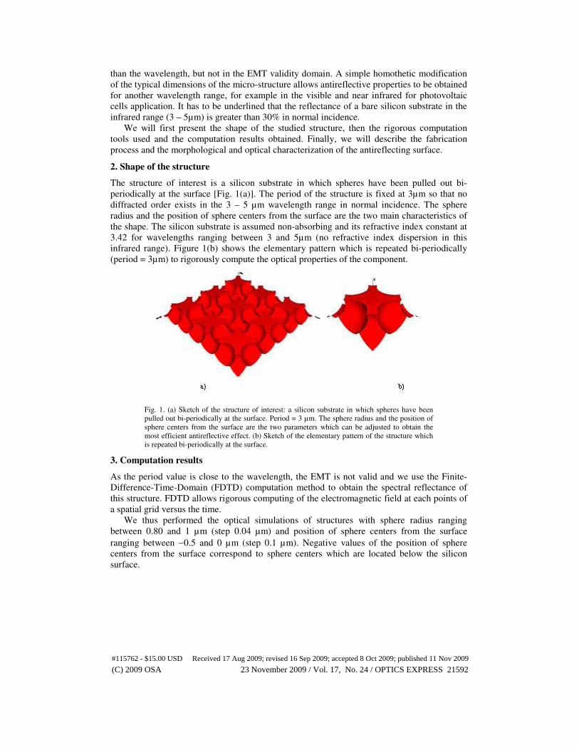
2. Shape of the structure
The structure of interest is a silicon substrate in which spheres have been pulled out bi-
periodically at the surface [Fig. 1(a)]. The period of the structure is fixed at 3µm so that no
diffracted order exists in the 3 – 5 µm wavelength range in normal incidence. The sphere
radius and the position of sphere centers from the surface are the two main characteristics of
the shape. The silicon substrate is assumed non-absorbing and its refractive index constant at
3.42 for wavelengths ranging between 3 and 5µm (no refractive index dispersion in this
infrared range). Figure 1(b) shows the elementary pattern which is repeated bi-periodically
(period = 3µm) to rigorously compute the optical properties of the component.
Fig. 1. (a) Sketch of the structure of interest: a silicon substrate in which spheres have been
pulled out bi-periodically at the surface. Period = 3 µm. The sphere radius and the position of
sphere centers from the surface are the two parameters which can be adjusted to obtain the
most efficient antireflective effect. (b) Sketch of the elementary pattern of the structure which
is repeated bi-periodically at the surface.
3. Computation results
As the period value is close to the wavelength, the EMT is not valid and we use the Finite-
Difference-Time-Domain (FDTD) computation method to obtain the spectral reflectance of
this structure. FDTD allows rigorous computing of the electromagnetic field at each points of
a spatial grid versus the time.
We thus performed the optical simulations of structures with sphere radius ranging
between 0.80 and 1 µm (step 0.04 µm) and position of sphere centers from the surface
ranging between −0.5 and 0 µm (step 0.1 µm). Negative values of the position of sphere
centers from the surface correspond to sphere centers which are located below the silicon
surface.
#115762 - $15.00 USD Received 17 Aug 2009; revised 16 Sep 2009; accepted 8 Oct 2009; published 11 Nov 2009
(C) 2009 OSA 23 November 2009 / Vol. 17, No. 24 / OPTICS EXPRESS 21592
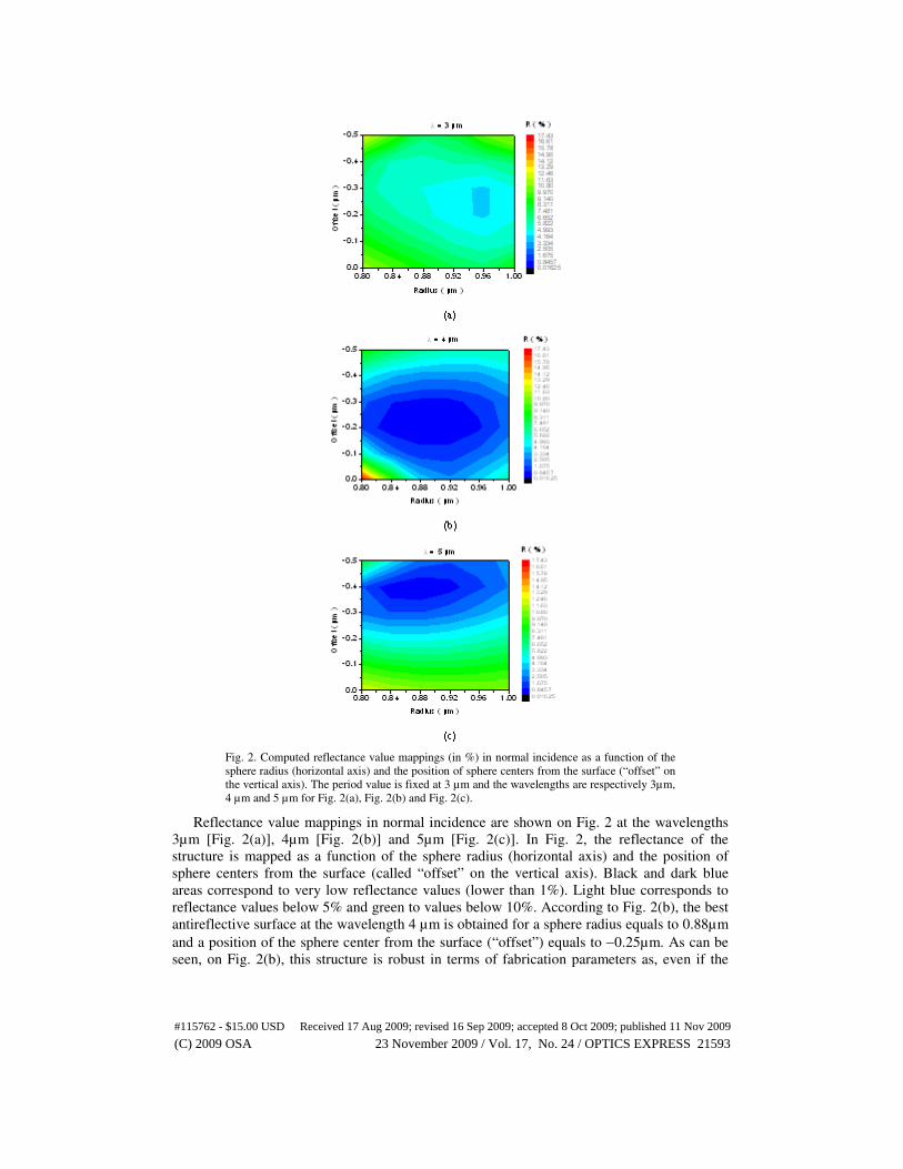
Fig. 2. Computed reflectance value mappings (in %) in normal incidence as a function of the
sphere radius (horizontal axis) and the position of sphere centers from the surface (“offset” on
the vertical axis). The period value is fixed at 3 µm and the wavelengths are respectively 3µm,
4 µm and 5 µm for Fig. 2(a), Fig. 2(b) and Fig. 2(c).
Reflectance value mappings in normal incidence are shown on Fig. 2 at the wavelengths
3µm [Fig. 2(a)], 4µm [Fig. 2(b)] and 5µm [Fig. 2(c)]. In Fig. 2, the reflectance of the
structure is mapped as a function of the sphere radius (horizontal axis) and the position of
sphere centers from the surface (called “offset” on the vertical axis). Black and dark blue
areas correspond to very low reflectance values (lower than 1%). Light blue corresponds to
reflectance values below 5% and green to values below 10%. According to Fig. 2(b), the best
antireflective surface at the wavelength 4 µm is obtained for a sphere radius equals to 0.88µm
and a position of the sphere center from the surface (“offset”) equals to −0.25µm. As can be
seen, on Fig. 2(b), this structure is robust in terms of fabrication parameters as, even if the
#115762 - $15.00 USD Received 17 Aug 2009; revised 16 Sep 2009; accepted 8 Oct 2009; published 11 Nov 2009
(C) 2009 OSA 23 November 2009 / Vol. 17, No. 24 / OPTICS EXPRESS 21593

sphere radius or the position of the sphere center are varied by +/− 0.1 µm, the reflectance
remains in the “blue region”, that is below 5%.
Thus, for these specific parameters (sphere radius = 0.88µm and position of the sphere
center from the surface = −0.25µm), we computed the reflectance in normal incidence over
the wavelengths ranging between 3 and 5 µm [Fig. 3(a)].
Fig. 3. (a) Spectral reflectance values of the structure having a sphere radius = 0.88µm and a
position of the sphere centers from the surface = −0.25µm, in normal incidence. (b) Spectral
reflectance values of the structure having a sphere radius = 0.96µm and a position of the
sphere centers from the surface = −0.25µm, in normal incidence.
Figure 3(a) shows that the reflectance remains very low in the spectral range of interest
since the values are below 3% for wavelengths between 3.2 and 5 µm. Yet, we notice an
increase of the reflectance for the wavelength 3µm (5% reflectance). It is thus of interest to
consider the mappings shown on Figs. 2(a) and 2(c) respectively at the wavelength 3 and 5
µm. Indeed, by keeping a position of the sphere centers from the surface equals to −0.25µm
and selecting a sphere radius equals to 0.96 µm instead of 0.88 µm, we obtain a reflectance
lower than 4% at the wavelength 3µm [see Fig. 2(a)], lower than 1% at the wavelength 4µm
[see Fig. 2(b)] and lower than 4% at the wavelength 5µm [see Fig. 2(c)]. The computed
spectral reflectance values of the structure having a sphere radius of 0.96 µm and a position
of the sphere centers from the surface equals to −0.25µm are summarized on Fig. 3(b). The
reflectance value at the wavelength 3.5 µm is extremely low at only 0.16% and the
reflectance is only 0.7% at the wavelength 4µm.
As demonstrated by computation, the antireflective effect obtained using such a pattern of
the silicon surface is highly efficient in term of minimal reflectance value reached but also in
term of spectral acceptance. It is thus natural to try to define a process allowing such kind of
structure to be fabricated.
4. Fabrication and morphological characterization
Standard Shipley S1818 photoresist was spun onto an oxidized (100) mono-crystalline silicon
wafers. After a hot-plate annealing (120°C during 30”), the photoresist was illuminated
through a classic photolithography mask composed of bi-periodic 0.75µm side square
apertures (period 3 µm). The photoresist was then developed and acid was used to etch the
silica through the photoresist mask. Acid etching was stopped as soon as de-wetting was seen
in the silica apertures that is when the silicon surface was reached. The rest of photoresist was
removed by acetone to obtain a silica mask, composed by the bi-periodic 0.75µm side square
apertures (period 3 µm), onto the silicon surface. Finally, low energy plasma reactive ion
etching was used to obtain isotropic silicon etching through the apertures of the silica mask.
The plasma was obtained using SF6 gas introduced with a 30 cm3/min flow. The plasma
power was 50 watts and the pressure 2.10−2
mbar. After a total removing of the rest of silica
#115762 - $15.00 USD Received 17 Aug 2009; revised 16 Sep 2009; accepted 8 Oct 2009; published 11 Nov 2009
(C) 2009 OSA 23 November 2009 / Vol. 17, No. 24 / OPTICS EXPRESS 21594
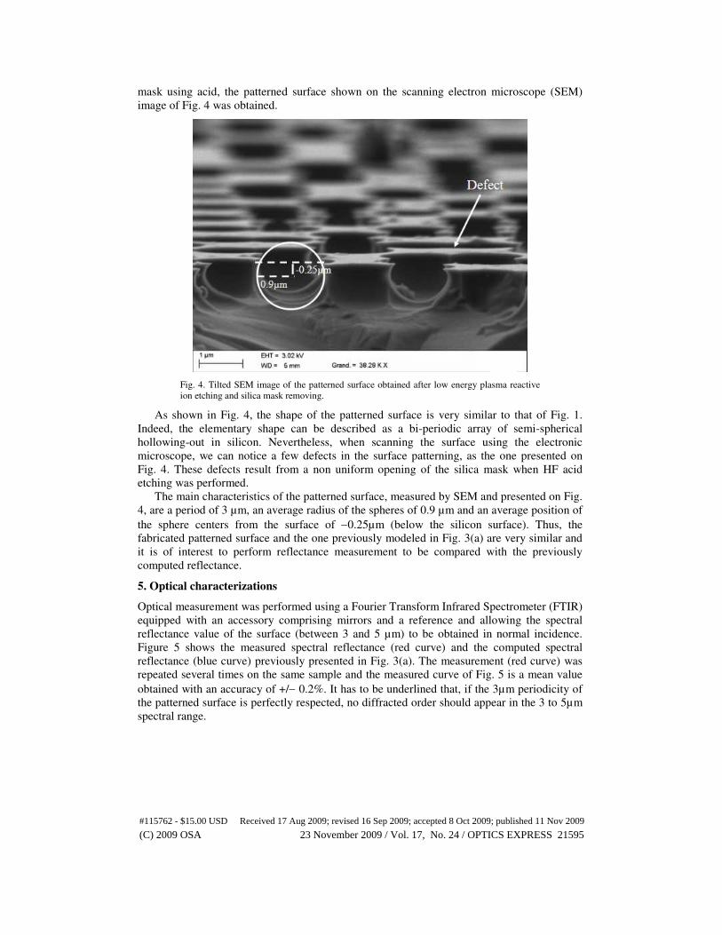
mask using acid, the patterned surface shown on the scanning electron microscope (SEM)
image of Fig. 4 was obtained.
Fig. 4. Tilted SEM image of the patterned surface obtained after low energy plasma reactive
ion etching and silica mask removing.
As shown in Fig. 4, the shape of the patterned surface is very similar to that of Fig. 1.
Indeed, the elementary shape can be described as a bi-periodic array of semi-spherical
hollowing-out in silicon. Nevertheless, when scanning the surface using the electronic
microscope, we can notice a few defects in the surface patterning, as the one presented on
Fig. 4. These defects result from a non uniform opening of the silica mask when HF acid
etching was performed.
The main characteristics of the patterned surface, measured by SEM and presented on Fig.
4, are a period of 3 µm, an average radius of the spheres of 0.9 µm and an average position of
the sphere centers from the surface of −0.25µm (below the silicon surface). Thus, the
fabricated patterned surface and the one previously modeled in Fig. 3(a) are very similar and
it is of interest to perform reflectance measurement to be compared with the previously
computed reflectance.
5. Optical characterizations
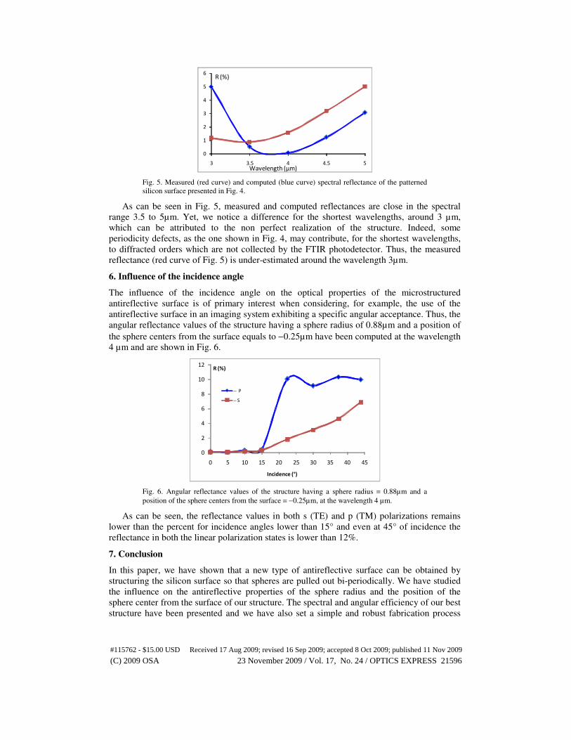
Optical measurement was performed using a Fourier Transform Infrared Spectrometer (FTIR)
equipped with an accessory comprising mirrors and a reference and allowing the spectral
reflectance value of the surface (between 3 and 5 µm) to be obtained in normal incidence.
Figure 5 shows the measured spectral reflectance (red curve) and the computed spectral
reflectance (blue curve) previously presented in Fig. 3(a). The measurement (red curve) was
repeated several times on the same sample and the measured curve of Fig. 5 is a mean value
obtained with an accuracy of +/− 0.2%. It has to be underlined that, if the 3µm periodicity of
the patterned surface is perfectly respected, no diffracted order should appear in the 3 to 5µm
spectral range.
#115762 - $15.00 USD Received 17 Aug 2009; revised 16 Sep 2009; accepted 8 Oct 2009; published 11 Nov 2009
(C) 2009 OSA 23 November 2009 / Vol. 17, No. 24 / OPTICS EXPRESS 21595
0
1
2
3
4
5
6
3 3.5 4 4.5 5
R (%)
Wavelength (µm)
Fig. 5. Measured (red curve) and computed (blue curve) spectral reflectance of the patterned
silicon surface presented in Fig. 4.
As can be seen in Fig. 5, measured and computed reflectances are close in the spectral
range 3.5 to 5µm. Yet, we notice a difference for the shortest wavelengths, around 3 µm,
which can be attributed to the non perfect realization of the structure. Indeed, some
periodicity defects, as the one shown in Fig. 4, may contribute, for the shortest wavelengths,
to diffracted orders which are not collected by the FTIR photodetector. Thus, the measured
reflectance (red curve of Fig. 5) is under-estimated around the wavelength 3µm.
6. Influence of the incidence angle
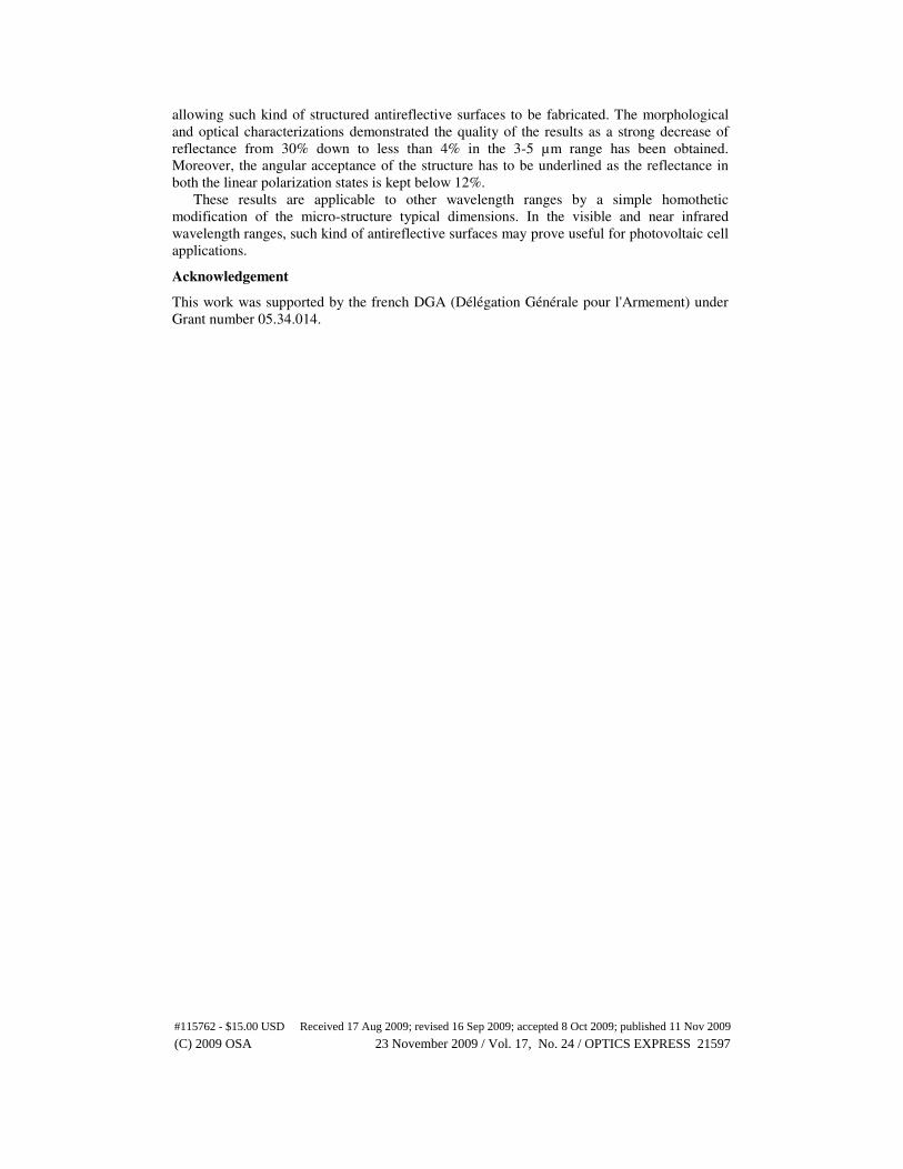
The influence of the incidence angle on the optical properties of the microstructured
antireflective surface is of primary interest when considering, for example, the use of the
antireflective surface in an imaging system exhibiting a specific angular acceptance. Thus, the
angular reflectance values of the structure having a sphere radius of 0.88µm and a position of
the sphere centers from the surface equals to −0.25µm have been computed at the wavelength
4 µm and are shown in Fig. 6.
0
2
4
6
8
10
12
0 5 10 15 20 25 30 35 40 45
-- P
-- S
Incidence (°)
R (%)
Fig. 6. Angular reflectance values of the structure having a sphere radius = 0.88µm and a
position of the sphere centers from the surface = −0.25µm, at the wavelength 4 µm.
As can be seen, the reflectance values in both s (TE) and p (TM) polarizations remains
lower than the percent for incidence angles lower than 15° and even at 45° of incidence the
reflectance in both the linear polarization states is lower than 12%.
7. Conclusion
In this paper, we have shown that a new type of antireflective surface can be obtained by
structuring the silicon surface so that spheres are pulled out bi-periodically. We have studied
the influence on the antireflective properties of the sphere radius and the position of the
sphere center from the surface of our structure. The spectral and angular efficiency of our best
structure have been presented and we have also set a simple and robust fabrication process
#115762 - $15.00 USD Received 17 Aug 2009; revised 16 Sep 2009; accepted 8 Oct 2009; published 11 Nov 2009
(C) 2009 OSA 23 November 2009 / Vol. 17, No. 24 / OPTICS EXPRESS 21596
allowing such kind of structured antireflective surfaces to be fabricated. The morphological
and optical characterizations demonstrated the quality of the results as a strong decrease of
reflectance from 30% down to less than 4% in the 3-5 µm range has been obtained.
Moreover, the angular acceptance of the structure has to be underlined as the reflectance in
both the linear polarization states is kept below 12%.
These results are applicable to other wavelength ranges by a simple homothetic
modification of the micro-structure typical dimensions. In the visible and near infrared
wavelength ranges, such kind of antireflective surfaces may prove useful for photovoltaic cell
applications.
Acknowledgement
This work was supported by the french DGA (Délégation Générale pour l'Armement) under
Grant number 05.34.014.
#115762 - $15.00 USD Received 17 Aug 2009; revised 16 Sep 2009; accepted 8 Oct 2009; published 11 Nov 2009
(C) 2009 OSA 23 November 2009 / Vol. 17, No. 24 / OPTICS EXPRESS 21597