spectral control of thermal emission by periodic microstructured surfaces in the near-infrared...
TRANSCRIPT

Sai et al. Vol. 18, No. 7 /July 2001 /J. Opt. Soc. Am. A 1471
Spectral control of thermal emission byperiodic microstructured
surfaces in the near-infrared region
Hitoshi Sai, Hiroo Yugami, Yasuhiro Akiyama, Yoshiaki Kanamori, and Kazuhiro Hane
Graduate School of Engineering, Tohoku University, Aoba01, Aramaki, Aoba-ku, Sendai, 980-8579, Japan
Received August 9, 2000; revised manuscript received January 2, 2001; accepted January 5, 2001
Thermal emissive properties of microstructured surfaces are measured in the near-infrared region. Two-dimensional periodic microstructured surfaces with metal coatings are fabricated with Si anisotropic etchingand laser ablation techniques. The structural periods of the samples are 2.0 and 1.5 mm. Clear selective-emission bands are observed experimentally. This selective emission is attributed to the resonance effect be-tween the emissive field and the surface microstructures. In addition, numerical calculation computed withrigorous coupled-wave analysis (RCWA) is performed on the microstructured samples. The selective-emissionpeaks measured through experiments can be reproduced well by RCWA, and this result suggests strongly thatthe thermal radiation from periodic structures may have spatial coherence. It is confirmed that the surfacemicrostructure can be applied to the control of spectral emission from high-temperature materials. © 2001Optical Society of America
OCIS codes: 230.1950, 350.5610, 300.2140, 120.6780, 260.5740, 230.3990
1. INTRODUCTIONSpectral control of thermal radiation has been one of themost important issues in improving efficiency or savingenergy consumption in heating and lighting systems. Insome cases, sharp spectral control can be obtained withinductive multilayer coatings. However, spectrally con-trolled optical properties have come to be necessary in ahigh-temperature environment in which multilayer coat-ings are damaged and therefore not available. For in-stance, it is useful to fabricate high-efficiency incandes-cent lamps,1 selective emitters for thermophotovoltaic(TPV) applications,2 solar absorbers,3 and so on. In TPVgeneration systems, thermal radiation from emittersheated at a high temperature converts into electricitywith the use of narrow-bandgap photovoltaic (PV) cells.Selective emitters, whose emittance is high within the PVcell’s sensitive region and low outside it, have been stud-ied to raise the efficiency of TPV systems. For the pastdecade, rare-earth selective emitters have been developedby many researchers, emitters that utilize luminescentbands of some rare-earth ions as selective-emissionbands.4–6 Those emitters, however, have some draw-backs: The spectral position of the high-emission bandscannot be controlled, because it is unique to each kind ofrare earth; the width of the emission band is narrow; andtheir material is restricted to oxide ceramics or crystalswhose thermal conductivity is low. At present, their per-formance has not been good enough to produce high-efficiency TPV generation.
In the above-mentioned cases, periodic surface micro-structure is one of the attractive options for controllingspectral emittance at high temperatures. It has alsomany advantages, such as adjustability of the period,freedom of material choice, and so on. Recent develop-ments in the field of micromachining have made it pos-
0740-3232/2001/071471-06$15.00 ©
sible to manufacture periodic microstructures with thesize of light wavelengths. As a result, the resonance ef-fect between the electromagnetic field and the periodicmicrostructures has become one of the most promisingways to vary optical or emissive properties artificially.Hesketh and Zemel7,8 and Wang and Zemel9–11 have re-ported extensively on polarized spectral emittance fromone-dimensional Si lamellar gratings. Tang andBuckious12 and Mollar et al.13 have reported in detail onreflectance from two-dimensional (2D) metal gratings.These reports have demonstrated the detailed feature ofthermal emittance from grating structures and haveshown the possibility of controlling spectral emittancefrom metal surfaces, although the grating period is re-stricted to the midinfrared range in them. Regardingpractical applications of thermal emission from gratingstructures at high temperatures, Sugimoto et al. have re-ported on IR suppression in the incandescent light from asurface with submicrometer holes.14 Heinzel et al. havedemonstrated that thermal radiation from microstruc-tured W surfaces can be utilized for fabricating TPV se-lective emitters.15 However, there are very few reportson spectral emittance from periodic microstructuredmetal surfaces at high temperatures in visible or near-infrared (NIR) regions.
In this paper, we investigate the resonance effect be-tween the emissive fields and the periodic metal micro-structures at high temperatures in the NIR range. Weshow the experimental results on optical and emissiveproperties of two-dimensional (2D) series of reverse-pyramid cavities. The samples with periods of 2 and 1.5mm are fabricated by means of electron-beam lithographyand Si anisotropic wet etching. The results demonstratethat periodic surface microstructures can control emissiveproperties. In addition to reporting the experimental
2001 Optical Society of America

1472 J. Opt. Soc. Am. A/Vol. 18, No. 7 /July 2001 Sai et al.
study, we analyze spectral alternations of emissive prop-erties attributed to periodic microstructures with rigorouscoupled wave analysis (RCWA).16–18 The results ofRCWA calculations agree well with the experimental re-sults.
2. EXPERIMENTA. Sample PreparationIn this paper, we focus on the resonance effect betweenthe thermal radiative field and 2D-periodic microstruc-tures in the NIR range of wavelengths l. For experimen-tal evaluation, it is necessary to fabricate microstructureswith a structural period L of NIR wavelengths. As abase material, we select a Si single-crystalline wafer, onwhich various microstructures can be processed relativelyeasily through some semiconductor micromachining tech-niques. In addition, the melting point of Si (1683 K) ishigh enough to heat up at measurement on emissive prop-erties. Considering the spectral response of the PV cellsfor TPV power generation ( for example, GaSb andInGaAs, etc.), we choose 2.0 and 1.5 mm as L.
We fabricate the periodic microstructured surfaces bythe following procedure, as shown in Fig. 1. First, a SiO2thin film is fabricated on a 2-in. Si single-crystalline wa-fer with (100) surface by oxidation. After a resist coatingis added, a microcross stripes pattern with a period L isdrawn on the resist film with electron-beam lithography.Then the developed wafer is soaked in a hydrogen fluoridesolution to remove the bare part of the SiO2 film. Themicrostructured SiO2 mask is thusly fabricated on the Siwafer. Next, the developed resist is eliminated, and thewafer is soaked in a tetramethylammonium hydroxide(TMAH) solution, which etches Si selectively. Since theSiO2 mask has good adhesiveness to Si, the mask patternis replicated to Si surface without side etching. Further-more, TMAH etches the Si crystal anisotropically, be-cause the etching rate for the (100) plane is approxi-mately 200 times faster than that of the (111) plane. Asa result, the uncovered Si surface is etched into a reverse-
Fig. 1. 2D periodic surface microstructures are fabricated byfollowing procedure: (1) oxidation, (2) resist coating, (3)electron-beam lithography and development, (4) SiO2 etching, (5)resist removing and Si anisotropic selective etching, (6) removingSiO2 mask and Pt sputtering.
pyramid shape composed of four (111) surfaces. Finally,after etching the SiO2 mask, the thin Pt layer is sputteredby laser abrasion method so as to enhance the effect of themicrostructured surfaces. Thus the periodic microstruc-tures with reverse-pyramid cavities are fabricated on Sisurfaces. This fabrication process has been alreadywidely applied for textured surfaces on Si PV cells; how-ever, the structural periods of our samples is muchsmaller than conventional texture surfaces.
Figure 2 shows scanning electron microscope (SEM)images of microstructured Si surfaces with L 5 2.0 mmfabricated by the above procedure. The base length andheight of a reverse-pyramid cavity are approximately 1.6and 1.1 mm, respectively. We can control those values byvarying the width of SiO2 microstripes, that is, by varyingthe etching time with hydrogen fluoride solutions. Thethickness of Pt film is ;37 nm. Using these values, wechoose parameters of a model structure for RCWA simu-lation. SEM observations have clarified that an orderly2D series of microcavities can be obtained without anydisorders.
Fig. 2. SEM pictures of the 2D periodic surface microstructureswith reverse-pyramid cavities (L 5 2.0 mm). (a) top view, (b)cross-sectional view.
Sai et al. Vol. 18, No. 7 /July 2001 /J. Opt. Soc. Am. A 1473
B. Experimental ApparatusThe schematic diagram of the apparatus used for emis-sive property measurement is shown in Fig. 3. Speci-mens are heated on a SiC electric heater in a vacuumchamber to prevent them from being oxidized. The tem-perature is varied from 300 to 900 K. After heating, wehave found no remarkable change on the sample surfacesthrough SEM observations. A CaF2 window, which hassuperior transmissivity from UV to IR wavelengths, isused as an optical window of the vacuum chamber.Emission from a sample passes through a pinhole and en-ters a Fourier transform infrared spectrophotometer,which has two kinds of detectors: TGS and InSb detec-tors. The former has a wide dynamic range and is suit-able for measurement in a broad range of wavelengths.On the other hand, the latter has high sensitivity in theNIR region, but its linear response range is narrowerthan the TGS detector. They can be switched optionallyunder experiment.
A measured emission spectrum is converted into anemissive power spectrum having the absolute value bymultiplying an apparatus coefficient spectrum. The ap-paratus coefficient is measured with a standard black-body furnace to calibrate the linearity of the detectors andevaluate the absolute emissive intensity. At the mea-surement of the apparatus coefficient, we ignore thevacuum region along the sample’s optical path, because itis much shorter than the total path length, and there isno strong absorption by the atmosphere near the wave-lengths focused on in this paper.
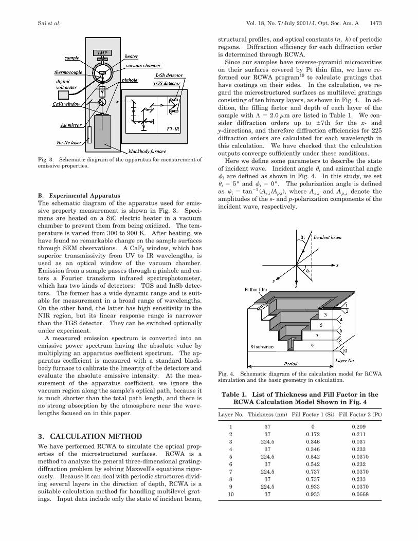
3. CALCULATION METHODWe have performed RCWA to simulate the optical prop-erties of the microstructured surfaces. RCWA is amethod to analyze the general three-dimensional grating-diffraction problem by solving Maxwell’s equations rigor-ously. Because it can deal with periodic structures divid-ing several layers in the direction of depth, RCWA is asuitable calculation method for handling multilevel grat-ings. Input data include only the state of incident beam,
Fig. 3. Schematic diagram of the apparatus for measurement ofemissive properties.
structural profiles, and optical constants (n, k) of periodicregions. Diffraction efficiency for each diffraction orderis determined through RCWA.
Since our samples have reverse-pyramid microcavitieson their surfaces covered by Pt thin film, we have re-formed our RCWA program19 to calculate gratings thathave coatings on their sides. In the calculation, we re-gard the microstructured surfaces as multilevel gratingsconsisting of ten binary layers, as shown in Fig. 4. In ad-dition, the filling factor and depth of each layer of thesample with L 5 2.0 mm are listed in Table 1. We con-sider diffraction orders up to 67th for the x- andy-directions, and therefore diffraction efficiencies for 225diffraction orders are calculated for each wavelength inthis calculation. We have checked that the calculationoutputs converge sufficiently under these conditions.
Here we define some parameters to describe the stateof incident wave. Incident angle u i and azimuthal anglef i are defined as shown in Fig. 4. In this study, we setu i 5 5° and f i 5 0°. The polarization angle is definedas c i 5 tan21 (As,i /Ap,i), where As,i and Ap,i denote theamplitudes of the s- and p-polarization components of theincident wave, respectively.
Fig. 4. Schematic diagram of the calculation model for RCWAsimulation and the basic geometry in calculation.
Table 1. List of Thickness and Fill Factor in theRCWA Calculation Model Shown in Fig. 4
Layer No. Thickness (nm) Fill Factor 1 (Si) Fill Factor 2 (Pt)
1 37 0 0.2092 37 0.172 0.2113 224.5 0.346 0.0374 37 0.346 0.2335 224.5 0.542 0.03706 37 0.542 0.2327 224.5 0.737 0.03708 37 0.737 0.2339 224.5 0.933 0.037010 37 0.933 0.0668

1474 J. Opt. Soc. Am. A/Vol. 18, No. 7 /July 2001 Sai et al.
4. RESULTS AND DISCUSSIONA. Reflectance and Transmittance SpectraFigure 5 shows the reflectance spectrum of the micro-structured sample with L 5 2.0 mm measured at roomtemperature. The angle u i is set to 5° in the experiment.The reflectance spectrum measured on a flat sample isalso shown in the figure as a reference. Those reflectionspectra are measured under random polarization. A sig-nificant dip appears in the spectrum of microstructuredsample at the wavelength l 5 1.96 mm, which is a littleshorter than L. This is attributed to the resonance effectbetween the surface microstructures and the electromag-netic field. Reflectance at the dip is ten times as low asthat for the flat sample.
With use of the optical constants of Pt and Si shown inthe literature,20,21 RCWA calculation is performed tosimulate the reflectance spectra of the microstructuredsample with L 5 2.0 mm. The result is shown in Fig. 5by the solid curve with circles. Since we used the normalreflection configuration in the experiment, the spectrumof the zeroth-order reflection efficiency is plotted in thefigure. The simulation reveals that the reflection spec-trum depends on c i in the range of l ' L, whereas wecannot analyze c i dependence of reflection through theexperiment because the incident beam is randomly polar-ized. We have found by calculation that the spectralshape at l ' L varies smoothly from c i 5 0° to 90°.Taking into account this result, we compare the measuredspectra with those calculated with c i 5 45°. The calcu-lated values agree quantitatively very well with the mea-sured spectrum.
The calculation shows that reflection efficiencies athigher diffraction orders are not zero, but they are quite abit smaller than those at the zeroth order in the wave-length range shown in Fig. 5. Furthermore, it is ob-tained from experimental and simulation studies that thetransmittance of the structured sample is lower than0.5% for all wavelengths shown in Fig. 5. This meansthat the transmittance can be ignored in this sample.Combining these facts with the general relationship
a~l! 5 1 2 r~l! 2 t~l!, (1)
where a is an absorptance, r is a reflectance, and t is atransmittance, it is confirmed that the microstructuredsurfaces have an energy absorption band at the resonancewavelength l ' L. Consequently, they are expected tohave a high emittance at the band.
B. Emissive PropertiesFigure 6 shows normal emissive power spectra of the mi-crostructured surfaces with L 5 2.0 mm at two differenttemperatures. Emissive power spectra of the flat sampleat similar temperatures are also shown in the figure.The TGS detector is used for the measurement of thosespectra. Comparing the microstructured sample withthe flat specimen, we can observe remarkable increases ofemission intensity in the range of l , 3 mm. The differ-ence between the structured samples’ emission and flatsamples’ emission increases with increasing temperature.
The spectral normal emittances e measured on threesamples, i.e., microstructured with L 5 2.0, 1.5 mm, and
flat samples, are shown in Fig. 7. The samples with themicrostructured surfaces show clear high e peaks. Thewavelength of observed peak position is close to the Lvalue of each sample. From the result, we conclude thatthose e peaks originate from the resonance effect betweenthe microstructures and the emissive field.
Owing to low sensitivity of the TGS detector in the NIRregion, we could not obtain emittance spectra with highsignal-to-noise ratio for l , 2 mm, as shown in Fig. 7.To investigate fine structures of spectra, we also mea-sured emissive spectra using the InSb detector for l, 2.5 mm. Figure 8(a) shows emissive power spectrameasured on the sample of L 5 2.0 mm at T 5 770 K and905 K. Several structures can be seen in the wavelengthrange for 1.4–2.3 mm. To emphasize the structures, thefirst derivatives of emissive power spectra are shown inFig. 8(b). Several distinct peaks at l 5 2.21, 2.02, 1.95,1.79, and 1.74 mm are observed in the figure. It is foundthat the position of these peaks is independent of tem-perature. Since these structures are observed in the
Fig. 5. Reflectance spectra of the microstructured (L5 2.0 mm) and the flat sample. Solid and dashed curves, mea-sured spectra for random polarized incident beam. Solid curvewith circles, calculated spectrum.
Fig. 6. Emissive power spectra of the microstructured (L5 2.0 mm) and flat samples measured at two different tempera-tures with the TGS detector.

Sai et al. Vol. 18, No. 7 /July 2001 /J. Opt. Soc. Am. A 1475
resonance wavelength region, they can be attributed tothe eigenmodes created by the 2D-periodic series of micro-cavities. The positions of these peaks do not agree com-pletely with those predicted by waveguide model, aspointed out by Wang and Zemel.9
Using the RCWA technique, we calculate diffraction ef-ficiencies up to 67th diffraction orders. Absorptance a ofthe microstructured sample is estimated from the follow-ing equation:
Fig. 7. Emittance spectra of the microstructured (L5 2.0 mm,1.5 mm) and flat samples measured with the TGS de-tector.
Fig. 8. (a) Emissive power spectra of the microstructuredsample (L 5 2.0 mm) measured with the InSb detector. (b)First derivative spectra of (a).
a~l! 5 1 2 (i52n
n
(j52n
n
@DERi, j~l! 1 DETi, j~l!#, (2)
where DERi,j is the (i, j)th backward-diffraction (reflec-tion) efficiency, DETi,j is the (i, j)th forward diffraction(transmission) efficiency, and n is the maximum diffrac-tion order considered in the calculation (here, n 5 7).Supposing that Kirchhoff’s law is still satisfied in thiscase, the absorptance a and the emittance e of the sampleare equal. Hereafter, we compare and consider the mea-sured e and the calculated a of the structured samplewith L 5 2.0 mm.
Figure 9 shows the normal e spectra measured on thesample of L 5 2.0 mm with the TGS detector. A calcu-lated a spectrum for the same sample with the param-eters of u i 5 5° and c i 5 45° is also shown in the figure.The overall feature of a calculated by RCWA is almostconsistent with that of measured e. The main peak posi-tions at l 5 2.2 and 2.0 mm in experimentally obtainedemission spectra can be especially well reproduced by thissimulation. This result strongly supports the idea thatthe thermal radiation from periodic structures has spatialcoherence.
In detail, however, the level of background of e is 0.1higher than that of a. This may be explained by the sur-face roughness and the temperature dependence of theoptical constants. In the RCWA analysis, we ignored thesurface roughness of the samples, which is observedthrough SEM.
Kirchhoff’s law holds well only at the same tempera-ture T:
a~l, T ! 5 e~l, T !. (3)
From Eq. (3) it is essential for accuracy to use the opticalconstants (n, k) at high temperatures in the calculation.As far as we know, however, there is no report on detailedoptical constants of Pt at high temperatures. Ujiharahas reported that reflectance of metals declined with ris-ing temperature.22 From Eq. (1), we see that a reductionof reflectance produces high absorptance. Experimen-
Fig. 9. Comparison of calculated absorptance and measuredemittance spectra of the microstructured sample (L 5 2.0 mm).The solid curve represents normal emittance spectrum measuredwith the TGS detector. The solid curve with circles representscalculated absorptance spectrum for u i 5 5° and c i 5 45°.

1476 J. Opt. Soc. Am. A/Vol. 18, No. 7 /July 2001 Sai et al.
tally we observed a reduction of Pt reflectance with risingtemperature. Therefore we speculate that the tempera-ture dependence of (n, k) is one of the main reasons forhigher background temperature in measured spectra ascompared with that in calculated spectra. The determi-nation of optical constants at high temperatures will bevery important in evaluating thermal emission propertiesof materials.
5. CONCLUSIONWe investigated the emissive properties of Pt films on the2D microstructured silicon surfaces. Selective emissiondue to the resonance effect between the emissive field andthe microstructure could be clearly obtained experimen-tally. Since the emittance peak varies with L, the sur-face microstructures can be applied in the control of emis-sive spectra. Numerical analysis with RCWA wascarried out, and it showed a good agreement with the ex-perimental results. It follows that the thermal emissionfrom periodic structures has spatial coherence. The mea-surement of optical constants at high temperaturesshould be performed to develop high-efficiency selectiveemitters.
ACKNOWLEDGMENTSThe authors thank Masao Chiba for his assistance withthe experiments. A part of this work was supported by aGrant-in-Aid for Scientific Research (B) (No. 11555057)from The Ministry of Education, Science, Sports, and Cul-ture of Japan. This study was carried out as a part of‘‘Ground Research Announcement for Space Utilization’’promoted by the Japan Space Forum. A part of this workwas performed in the Venture Business Laboratory in To-hoku University.
Corresponding author Hiroo Yugami can be reached atthe address on the title page or by e-mail at [email protected].
REFERENCES1. J. F. Waymouth, ‘‘Optical light source device,’’ U.S. patent
5,079,473, January 7, 1992.2. T. J. Coutts, ‘‘A review of progress in thermophotovoltaic
generation of electricity,’’ Renew. Sustain. Energy Rev. 3,77–184 (1999).
3. S. Hava and M. Auslender, ‘‘Design of analysis of low-reflection grating microstructures for a solar energy ab-sorber,’’ Sol. Energy Mater. Sol. Cells 61, 143–151 (2000).
4. D. L. Chubb, A. T. Pal, M. O. Patton, and P. P. Jenkins,‘‘Rare earth doped high temperature ceramic selective emit-ters,’’ J. Eur. Ceram. Soc. 19, 2551–2562 (1999).
5. M. G. Krishna, M. Rajendran, D. R. Pyke, and A. K. Bhat-tacharya, ‘‘Spectral emissivity of ytterbium oxide-based ma-terials for application as selective emitters in thermophoto-voltaic devices,’’ Sol. Energy Mater. Sol. Cells 59, 337–348(1999).
6. H. Sai, H. Yugami, K. Nakamura, N. Nakagawa, H. Oht-subo, and S. Maruyama, ‘‘Selective emission ofAl2O3 /Er3Al5O12 eutectic composite for thermophoto-voltaicgeneration of electricity,’’ Jpn. J. Appl. Phys., Part 1 39,1957–1961 (2000).
7. P. J. Hesketh and J. N. Zemel, ‘‘Polarized spectral emit-tance from periodic micromachined surfaces. I. Dopedsilicon: the normal direction,’’ Phys. Rev. B 37, 10795–10802 (1988).
8. P. J. Hesketh and J. N. Zemel, ‘‘Polarized spectral emit-tance from periodic micromachined surfaces. II. Dopedsilicon: angular variation,’’ Phys. Rev. B 37, 10803–10813(1988).
9. T. K. Wang and J. N. Zemel, ‘‘Polarized spectral emittancefrom periodic micromachined surfaces. III. Undoped sili-con: the normal direction in shallow lamellar gratings,’’Infrared Phys. 32, 477–488 (1991).
10. T. K. Wang and J. N. Zemel, ‘‘Polarized spectral emittancefrom periodic micromachined surfaces. IV. Undoped sili-con: normal direction in deep lamellar gratings,’’ Appl.Opt. 31, 732–736 (1992).
11. T. K. Wang and J. N. Zemel, ‘‘Polarized spectral emittancefrom periodic micromachined surfaces. V. Undoped sili-con: angular measurement in shallow lamellar gratings,’’Appl. Opt. 32, 2021–2025 (1993).
12. K. Tang and R. O. Buckious, ‘‘Bi-directional reflection mea-surements from two-dimensional microcontoured metallicsurfaces,’’ Microscale Thermophys. Eng. 2, 245–260 (1998).
13. K. D. Moller, K. R. Farmer, D. V. P. Ivanov, O. Sternberg,K. P. Stewart, and P. Lalanne, ‘‘Thin and thick crossshaped metal grids,’’ Infrared Phys. Technol. 40, 475–485(1999).
14. M. Sugimoto, T. Fujioka, T. Inoue, H. Fukushima, Y. Mi-zuyama, S. Ukegawa, T. Matsushima, and M. Toho, ‘‘Theinfra-red suppression in the incandescent light from a sur-face with submicron holes,’’ J. Light Visual Environ. 18,5–10 (1994).
15. A. Heinzel, V. Boerner, A. Gombert, V. Wittwer, and J.Luther, ‘‘Microstructured tungsten surfaces as selectiveemitters,’’ in Proceedings of the Thermophotovoltaic Gen-eration of Electricity 4th NREL Conference, Denver, Colo-rado, 1998, T. J. Coutts, J. P. Benner, and C. S. Allman,eds. (American Institute of Physics, New York, 1999), pp.191–196.
16. M. G. Moharam, ‘‘Coupled-wave analysis of two-dimensional Dielectric gratings,’’ in Holographic Optics:Design and Applications, I. Cindrich, ed., Proc. SPIE 883,8–11 (1988).
17. S. Peng and G. M. Morris, ‘‘Efficient implementation of rig-orous coupled-wave analysis,’’ J. Opt. Soc. Am. A 12, 1087–1096 (1995).
18. N. Chaetau and J.-P. Hugonin, ‘‘Algorithm for the rigorouscoupled-wave analysis of grating diffraction,’’ J. Opt. Soc.Am. A 11, 1321–1331 (1994).
19. Y. Kanamori, H. Kikuta, and K. Hane, ‘‘Broadband antire-flection gratings for glass substrates fabricated by fast atombeam etching,’’ Jpn. J. Appl. Phys. Part 2 39, L735–L737(2000).
20. D. W. Lynch and W. R. Hunter, Handbook of Optical Con-stants of Solids I, Part II, Subpart I: Metals, E. D. Palik,ed. (Academic, New York, 1985), pp. 334–341.
21. D. F. Edwards, Handbook of Optical Constants of Solids I,Part II, Subpart II: Semiconductors, E. D. Palik, ed. (Aca-demic, New York, 1985), pp. 547–569.
22. K. Ujihara, ‘‘Reflectivity of metals at high temperatures,’’ J.Appl. Phys. 43, 2376–2383 (1972).