specification · gip clks, dsc vout_led dvcc vled led_en pwm 768 1366 the lp156wh2 is a color...
TRANSCRIPT

Avnet Embedded. Support Around The Board™
www.avnet-embedded.eu
SpEcificATion
if you require a touch panel solution.For information ontouch sensors, sensor driving and touch panel bonding solutions, scan the QR code or click the URLwww.avnet-embedded.eu/products/displays/.html
LP156WH2
Date: August 2012
Product Specification
LP156WH2 Liquid Crystal Display
Ver. 0.0 Aug. 03, 2012 1 / 31
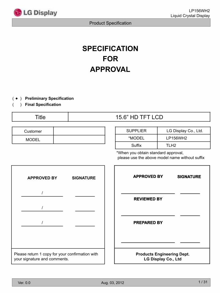
SPECIFICATION FOR
APPROVAL
Title 15.6” HD TFT LCD
Customer
MODEL
SUPPLIER LG Display Co., Ltd.
*MODEL LP156WH2
Suffix TLH2
*When you obtain standard approval, please use the above model name without suffix
( ) Preliminary Specification ( ) Final Specification ◆
Please return 1 copy for your confirmation with your signature and comments.
/
/
/
SIGNATURE APPROVED BY
PREPARED BY
REVIEWED BY
SIGNATURE APPROVED BY
Products Engineering Dept. LG Display Co., Ltd
PREPARED BY
REVIEWED BY
SIGNATURE APPROVED BY

Product Specification
LP156WH2 Liquid Crystal Display
Ver. 0.0 Aug. 03, 2012 2 / 31
Contents
No ITEM Page
COVER 1
CONTENTS 2
RECORD OF REVISIONS 3
1 GENERAL DESCRIPTION 4
2 ABSOLUTE MAXIMUM RATINGS 5
3 ELECTRICAL SPECIFICATIONS
3-1 ELECTRICAL CHARACTREISTICS 6-7
3-2 INTERFACE CONNECTIONS 8
3-3 LVDS SIGNAL TIMING SPECIFICATION 9-10
3-3 SIGNAL TIMING SPECIFICATIONS 11
3-4 SIGNAL TIMING WAVEFORMS 11
3-5 COLOR INPUT DATA REFERNECE 12
3-6 POWER SEQUENCE 13
4 OPTICAL SFECIFICATIONS 14-16
5 MECHANICAL CHARACTERISTICS 17-20
6 RELIABLITY 21
7 INTERNATIONAL STANDARDS
7-1 SAFETY 22
8 PACKING
8-1 DESIGNATION OF LOT MARK 23
8-2 PACKING FORM 23
A APPENDIX- 1, 2, 3 24-26
9 PRECAUTIONS 27-28
A APPENDIX. Enhanced Extended Display Identification Data 29-31

Product Specification
LP156WH2 Liquid Crystal Display
Ver. 0.0 Aug. 03, 2012 3 / 31
RECORD OF REVISIONS
Revision No Revision Date Page Description EDID ver
0.0 Aug. 3. 2012 - First Draft (Preliminary Specification) -
- -

Product Specification
LP156WH2 Liquid Crystal Display
Ver. 0.0 Aug. 03, 2012 4 / 31
1. General Description
General Features Active Screen Size 15.6 inches diagonal Outline Dimension 359.3(H, typ) × 209.5(V, typ) × 5.5(D,max) [mm] Pixel Pitch 0.252mm × 0.252 mm Pixel Format 1366 horiz. By 768 vert. Pixels RGB strip arrangement Color Depth 6-bit, 262,144 colors Luminance, White 500 cd/m2(Typ.5 point) Power Consumption Total 7.2 W (Typ.) @ LCM circuit 1.3 W (Typ.), B/L input 5.9 W (Typ.) Weight 455g (Typ.), 470g (Max.) Display Operating Mode Transmissive mode, normally white Surface Treatment Anti-Glare treatment of the front polarizer
RoHS Compliance Yes
BFR / PVC / As Free Yes for all
Control & Data Power EDID signal & Power
TFT-LCD Panel
(HD, DRD, TN)
1
Timing Control
(Tcon) Block
User connector
40 Pin
EEPROM Block for EDID
Source Driver (Bottom Bent)
LED Backlight Ass’y
TCLKs
LVDS 1port
VCC
LED Driver Block
FB
Power
Block
DVCC, AVDD VGH, VGL, GMA
GIP CLKs, DSC
VOUT_LED
DVCC
VLED
LED_EN PWM
768
1366
The LP156WH2 is a Color Active Matrix Liquid Crystal Display with an integral LED backlight system. The matrix employs a-Si Thin Film Transistor as the active element. It is a transmissive type display operating in the normally white mode. This TFT-LCD has 15.6 inches diagonally measured active display area with HD resolution (1366 horizontal by 768 vertical pixel array). Each pixel is divided into Red, Green and Blue sub-pixels or dots which are arranged in vertical stripes. Gray scale or the brightness of the sub-pixel color is determined with a 6-bit gray scale signal for each dot, thus, presenting a palette of more than 262,144 colors. The LP156WH2 has been designed to apply the interface method that enables low power, high speed, low EMI. The LP156WH2 is intended to support applications where thin thickness, low power are critical factors and graphic displays are important. In combination with the vertical arrangement of the sub-pixels, the LP156WH2 characteristics provide an excellent flat display for office automation products such as Notebook PC.
Product Specification
LP156WH2 Liquid Crystal Display
Ver. 0.0 Aug. 03, 2012 5 / 31
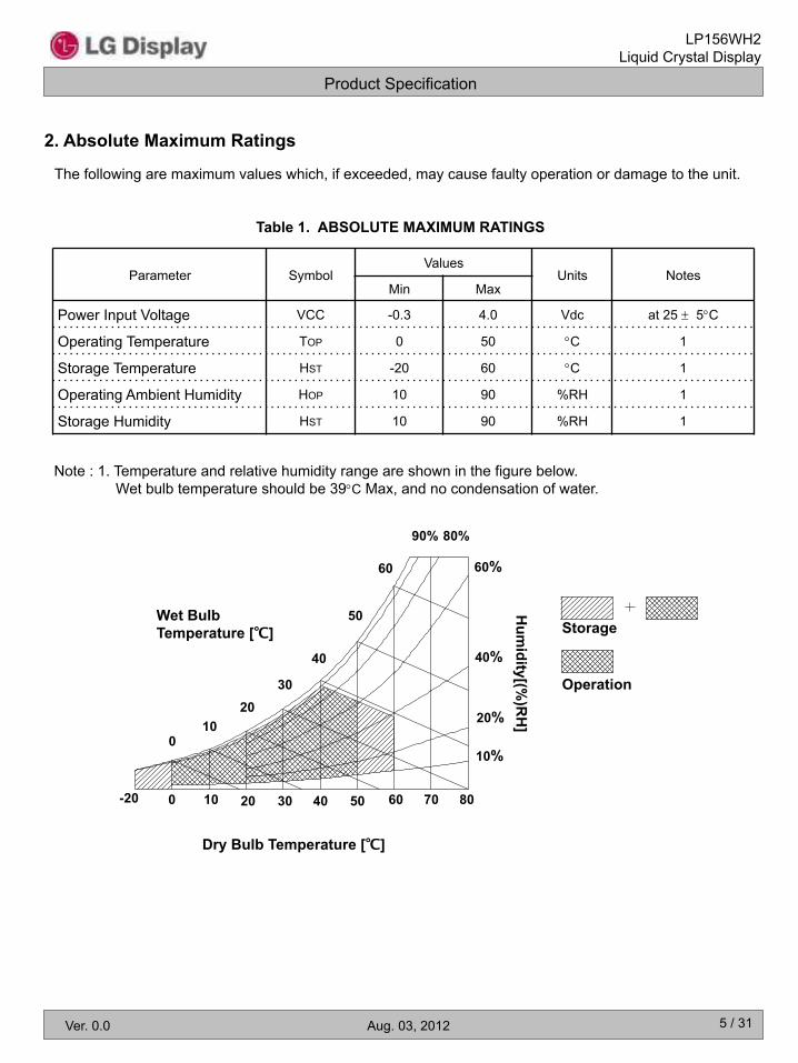
2. Absolute Maximum Ratings
The following are maximum values which, if exceeded, may cause faulty operation or damage to the unit.
Table 1. ABSOLUTE MAXIMUM RATINGS
Storage
Operation
10 20 30 40 50 60 70 80 0 -20
Dry Bulb Temperature [℃]
10%
20%
40%
60%
90% 80%
0 10
20 30
40
50
60
Wet Bulb Temperature [℃]
Hum
idity[(%)R
H]
Parameter Symbol Values
Units Notes Min Max
Power Input Voltage VCC -0.3 4.0 Vdc at 25 ± 5°C
Operating Temperature TOP 0 50 °C 1
Storage Temperature HST -20 60 °C 1
Operating Ambient Humidity HOP 10 90 %RH 1
Storage Humidity HST 10 90 %RH 1
Note : 1. Temperature and relative humidity range are shown in the figure below. Wet bulb temperature should be 39°C Max, and no condensation of water.

Product Specification
LP156WH2 Liquid Crystal Display
Ver. 0.0 Aug. 03, 2012 6 / 31
3. Electrical Specifications
3-1. Electrical Characteristics The LP156WH2 requires two power inputs. The first logic is employed to power the LCD electronics and to drive the TFT array and liquid crystal. The second backlight is the input about LED BL.with LED Driver.
Parameter Symbol Values
Unit Notes Min Typ Max
LOGIC :
Power Supply Input Voltage VCC 3.0 3.3 3.6 V 1
Power Supply Input Current (Even)
Mosaic ICC - 400 460 mA 2
Black ICC_max - 485 560 mA 3
Power Consumption PCC - 1.3 1.5 W 2
Power Supply Inrush Current ICC_P - - 1500 mA 4
LVDS Impedance ZLVDS 90 100 110 Ω 5
EDID Input Voltage VEDID 3.0 3.3 3.6 V
EDID Input Current IEDID - - 10 mA
BACKLIGHT : ( with LED Driver)
LED Power Input Voltage VLED 7.0 12.0 21.0 V 6
LED Power Input Current ILED - 490 535 mA 7
LED Power Consumption PLED - 5.9 6.3 W 7
LED Power Inrush Current ILED_P - - 1500 mA 8
PWM Duty Ratio 5 - 100 % 9
PWM Jitter - 0 - 0.3 % 10
PWM Impedance ZPWM 20 40 60 kΩ
PWM Frequency FPWM 200 - 1000 Hz 11
PWM High Level Voltage VPWM_H 3.0 - 5.3 V
PWM Low Level Voltage VPWM_L 0 - 0.3 V
LED_EN Impedance ZPWM 20 40 60 kΩ
LED_EN High Voltage VLED_EN_H 3.0 - 5.3 V
LED_EN Low Voltage VLED_EN_L 0 - 0.3 V
Life Time 15,000 - - Hrs 12
Table 2. ELECTRICAL CHARACTERISTICS
Product Specification
LP156WH2 Liquid Crystal Display
Ver. 0.0 Aug. 03, 2012 7 / 31
3. This Spec. is the max load condition for the cable impedance designing. (Measured by Multi-Meter = EVEN) 4. The below figures are the measuring Vcc condition and the Vcc control block LGD used. The Vcc condition is same the minimum of T1 at Power on sequence.
5. This impedance value is needed to proper display and measured form LVDS Tx to the mating connector. 6. The measuring position is the connector of LCM and the test conditions are under 25℃. 7. The current and power consumption with LED Driver are under the Vled = 12.0V , 25℃, Dimming of Max luminance whereas White pattern is displayed and fv is the frame frequency. 8. The below figures are the measuring VLED condition and the VLED control block LGD used. VLED control block is same with Vcc control block. 9. The operation of LED Driver below minimum dimming ratio may cause flickering or reliability issue. 10. If Jitter of PWM is bigger than maximum. It may cause flickering. 11. This Spec. is not effective at 100% dimming ratio as an exception because it has DC level equivalent to 0Hz. In spite of acceptable range as defined, the PWM Frequency should be fixed and stable for more consistent brightness control at any specific level desired. 12. The life time is determined as the time at which brightness of LED is 50% compare to that of minimum value specified in table 7. under general user condition.
10%
90%
0.5ms
3.3V
0V
10%
90%
0.5ms
12.0V
0V
Rising time Vcc
Rising time VLED
Note) 1. The measuring position is the connector of LCM and the test conditions are under 25℃, fv = 60Hz, Black pattern. 2. The specified Icc current and power consumption are under the Vcc = 3.3V , 25℃, fv = 60Hz condition whereas Mosaic pattern is displayed and fv is the frame frequency. (Max current pattern is Black, measured by Multi-Meter=EVEN)

Product Specification
LP156WH2 Liquid Crystal Display
Ver. 0.0 Aug. 03, 2012 8 / 31
3-2. Interface Connections
Table 3. MODULE CONNECTOR PIN CONFIGURATION (CN1) Pin Symbol Description Notes 1 NC No Connection. [Interface Chip]
1. LCD : SW, SW0624B (LCD Controller) including LVDS Receiver 2. System : THC63LVDF823A or equivalent * Pin to Pin compatible with LVDS [Connector] 20455-040E-0x, I-PEX KN38A-40S-0.5H, HIROSE [Mating Connector] 20453-040T, I-Pex or equivalent [Connector pin arrangement]
2 VCC LCD Logic and driver power (3.3V Typ.) 3 VCC LCD Logic and driver power (3.3V Typ.) 4 V EEDID DDC Power (3.3V) 5 NC No Connection. 6 Clk EEDID DDC Clock 7 DATA EEDID DDC Data 8 Odd_RIN 0- Negative LVDS differential data input 9 Odd_RIN 0+ Positive LVDS differential data input
10 GND LCM Ground 11 Odd_RIN 1- Negative LVDS differential data input 12 Odd_RIN 1+ Positive LVDS differential data input 13 GND LCM Ground 14 Odd_RIN 2- Negative LVDS differential data input 15 Odd_RIN 2+ Positive LVDS differential data input 16 GND LCM Ground 17 Odd_CLKIN- Negative LVDS differential clock input 18 Odd_CLKIN+ Positive LVDS differential clock input 19 GND LCM Ground 20 NC No Connection 21 NC No Connection 22 GND LCM Ground 23 NC No Connection 24 NC No Connection 25 GND LCM Ground 26 NC No Connection 27 NC No Connection 28 GND LCM Ground 29 NC No Connection 30 NC No Connection
31 VLED_GND LCM Ground (LED Backlight Ground)
32 VLED_GND LCM Ground (LED Backlight Ground)
33 VLED_GND LCM Ground (LED Backlight Ground)
34 NC No Connection. 35 BLIM System PWM Signal input for dimming
36 BL_On LED Backlight On/Off
37 NC No Connection
38 VLED LED Backlight Power (7V-21V)
39 VLED LED Backlight Power (7V-21V)
40 VLED LED Backlight Power (7V-21V)
[LCD Module Rear View]
1
40
This LCD employs two interface connections, a 40 pin connector used for the module electronics interface and the other connector used for the integral backlight system.

Product Specification
LP156WH2 Liquid Crystal Display
Ver. 0.0 Aug. 03, 2012 9 / 31
Description Symbol Min Max Unit Notes
LVDS Clock to Data Skew Margin tSKEW - 400 + 400 ps
85MHz > Fclk ≥ 65MHz
tSKEW - 600 + 600 ps 65MHz > Fclk ≥ 25MH
z
LVDS Clock to Clock Skew Margin (Even to Odd) tSKEW_EO - 1/7 + 1/7 Tclk -
Maximum deviation of input clock frequency during SSC
FDEV - ± 3 % -
Maximum modulation frequency of input clock during SSC
FMOD - 200 KHz -
Description Symbol Min Max Unit Notes
LVDS Differential Voltage |VID| 100 600 mV -
LVDS Common mode Voltage VCM 0.6 1.8 V -
LVDS Input Voltage Range VIN 0.3 2.1 V -
3-3-1. DC Specification
3-3-2. AC Specification
LVDS +
LVDS -
0V
VCM# |VID| = |(LVDS+) – (LVDS-)|# VCM = {(LVDS+) + (LVDS-)}/2
|VID|
VIN_MAX VIN_MIN
3-3. LVDS Signal Timing Specifications
LVDS Data
tSKEW
LVDS Clock
Tclk
tSKEW (Fclk = 1/Tclk) 1) 85MHz > Fclk ≥ 65MHz : -400 ~ +400 2) 65MHz > Fclk ≥ 25MHz : -600 ~ +600

Product Specification
LP156WH2 Liquid Crystal Display
Ver. 0.0 Aug. 03, 2012 10 / 31
LVDS Even Data
LVDS Odd Clock
LVDS Even Clock
tSKEW_EO
Tclk
Tclk
< Clock skew margin between channel >
< LVDS Data Format >
3-3-3. Data Format 1) LVDS 1 Port
< Spread Spectrum >
Time
Fcenter
Fmax
Fmin
FMOD
1
Fcenter * FDEV
Freq.
G 0 R 5 R 4 R 3 R 2 R 1 R 0
B 1 B 0 G 5 G 4 G 3 G 2 G 1
DE VSYNC HSYNC B 5 B 4 B 3 B 2
X B 7 B 6 G 7 G 6 R 7 R 6
R 1 R 0
G 2 G 1
B 3 B 2
R 7 R 6
G 0
B 1
DE
X
Current ( Nth ) Cycle
R 5 R 4
B 0 G 5
VSYNC HSYNC
B 7 B 6
R 3 R 2
G 4 G 3
B 5 B 4
G 7 G 6
Previous ( N - 1 ) th Cycle Next ( N + 1 ) th Cycle
RCLK+
RA+/-
RB+/-
RC+/-
RD+/-
Product Specification
LP156WH2 Liquid Crystal Display
Ver. 0.0 Aug. 03, 2012 11 / 31
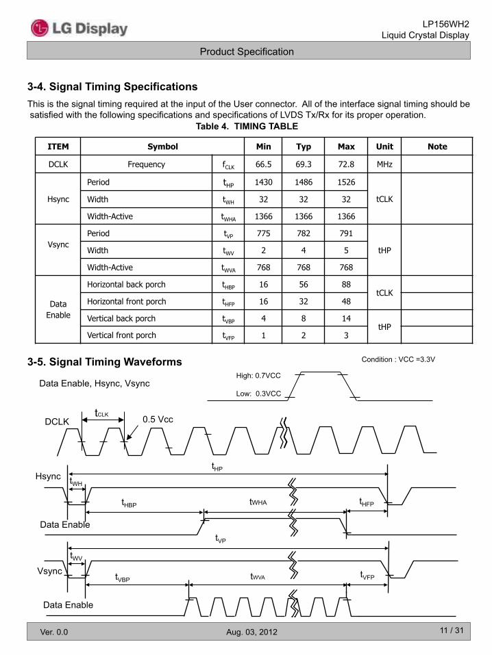
3-4. Signal Timing Specifications
Table 4. TIMING TABLE
This is the signal timing required at the input of the User connector. All of the interface signal timing should be satisfied with the following specifications and specifications of LVDS Tx/Rx for its proper operation.
3-5. Signal Timing Waveforms Condition : VCC =3.3V
Low: 0.3VCC
High: 0.7VCC Data Enable, Hsync, Vsync
Hsync
Data Enable
Vsync
Data Enable
tWH tHP
tHFP tHBP
tVP
tWV
tVBP tVFP
tWHA
tWVA
tCLK 0.5 Vcc DCLK
ITEM Symbol Min Typ Max Unit Note
DCLK Frequency fCLK 66.5 69.3 72.8 MHz
Hsync
Period tHP 1430 1486 1526
tCLK Width tWH 32 32 32
Width-Active tWHA 1366 1366 1366
Vsync
Period tVP 775 782 791
tHP Width tWV 2 4 5
Width-Active tWVA 768 768 768
Data Enable
Horizontal back porch tHBP 16 56 88 tCLK
Horizontal front porch tHFP 16 32 48
Vertical back porch tVBP 4 8 14 tHP
Vertical front porch tVFP 1 2 3
Product Specification
LP156WH2 Liquid Crystal Display
Ver. 0.0 Aug. 03, 2012 12 / 31
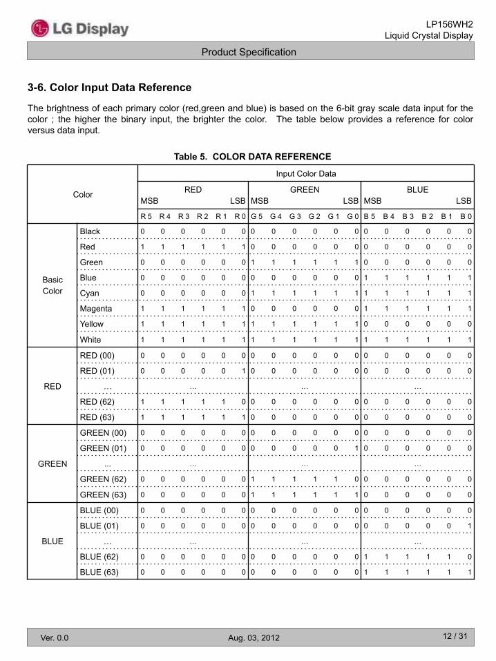
3-6. Color Input Data Reference
The brightness of each primary color (red,green and blue) is based on the 6-bit gray scale data input for the color ; the higher the binary input, the brighter the color. The table below provides a reference for color versus data input.
Table 5. COLOR DATA REFERENCE
Color
Input Color Data
RED MSB LSB
GREEN MSB LSB
BLUE MSB LSB
R 5 R 4 R 3 R 2 R 1 R 0 G 5 G 4 G 3 G 2 G 1 G 0 B 5 B 4 B 3 B 2 B 1 B 0
Basic Color
Black 0 0 0 0 0 0 0 0 0 0 0 0 0 0 0 0 0 0
Red 1 1 1 1 1 1 0 0 0 0 0 0 0 0 0 0 0 0
Green 0 0 0 0 0 0 1 1 1 1 1 1 0 0 0 0 0 0
Blue 0 0 0 0 0 0 0 0 0 0 0 0 1 1 1 1 1 1
Cyan 0 0 0 0 0 0 1 1 1 1 1 1 1 1 1 1 1 1
Magenta 1 1 1 1 1 1 0 0 0 0 0 0 1 1 1 1 1 1
Yellow 1 1 1 1 1 1 1 1 1 1 1 1 0 0 0 0 0 0
White 1 1 1 1 1 1 1 1 1 1 1 1 1 1 1 1 1 1
RED
RED (00) 0 0 0 0 0 0 0 0 0 0 0 0 0 0 0 0 0 0
RED (01) 0 0 0 0 0 1 0 0 0 0 0 0 0 0 0 0 0 0
… … … …
RED (62) 1 1 1 1 1 0 0 0 0 0 0 0 0 0 0 0 0 0
RED (63) 1 1 1 1 1 1 0 0 0 0 0 0 0 0 0 0 0 0
GREEN
GREEN (00) 0 0 0 0 0 0 0 0 0 0 0 0 0 0 0 0 0 0
GREEN (01) 0 0 0 0 0 0 0 0 0 0 0 1 0 0 0 0 0 0
... … … …
GREEN (62) 0 0 0 0 0 0 1 1 1 1 1 0 0 0 0 0 0 0
GREEN (63) 0 0 0 0 0 0 1 1 1 1 1 1 0 0 0 0 0 0
BLUE
BLUE (00) 0 0 0 0 0 0 0 0 0 0 0 0 0 0 0 0 0 0
BLUE (01) 0 0 0 0 0 0 0 0 0 0 0 0 0 0 0 0 0 1
… … … …
BLUE (62) 0 0 0 0 0 0 0 0 0 0 0 0 1 1 1 1 1 0
BLUE (63) 0 0 0 0 0 0 0 0 0 0 0 0 1 1 1 1 1 1
Product Specification
LP156WH2 Liquid Crystal Display
Ver. 0.0 Aug. 03, 2012 13 / 31
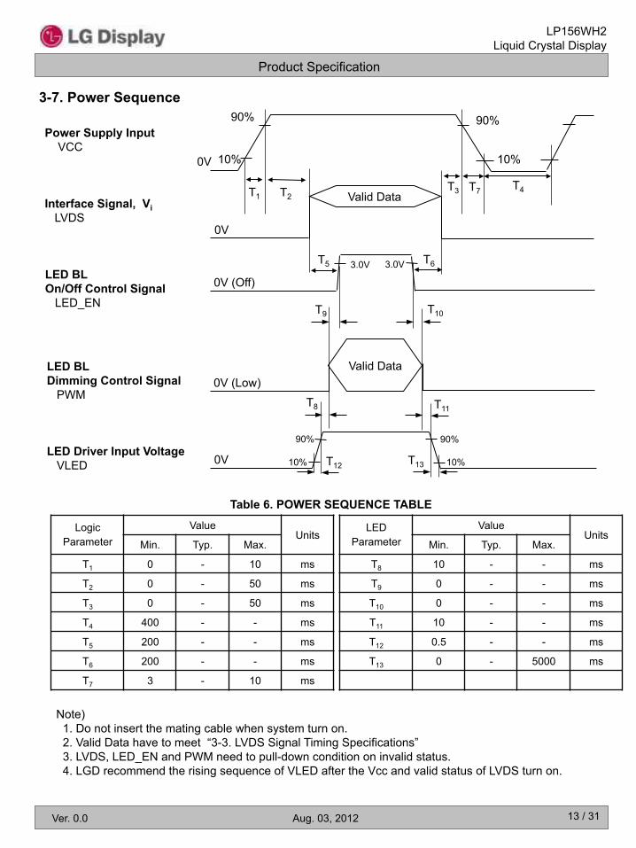
Note) 1. Do not insert the mating cable when system turn on. 2. Valid Data have to meet “3-3. LVDS Signal Timing Specifications” 3. LVDS, LED_EN and PWM need to pull-down condition on invalid status. 4. LGD recommend the rising sequence of VLED after the Vcc and valid status of LVDS turn on.
Table 6. POWER SEQUENCE TABLE
LED Parameter
Value Units
Min. Typ. Max.
T8 10 - - ms
T9 0 - - ms
T10 0 - - ms
T11 10 - - ms
T12 0.5 - - ms
T13 0 - 5000 ms
3-7. Power Sequence
Logic Parameter
Value Units
Min. Typ. Max.
T1 0 - 10 ms
T2 0 - 50 ms
T3 0 - 50 ms
T4 400 - - ms
T5 200 - - ms
T6 200 - - ms
T7 3 - 10 ms
T7 Interface Signal, Vi LVDS
Power Supply Input VCC
90%
10% 10% 0V
90%
T1 T2 T3 T4
T5 T6
0V
LED BL Dimming Control Signal PWM
0V (Low) T8
LED Driver Input Voltage VLED
T10
LED BL On/Off Control Signal LED_EN
T11
T9
Valid Data
0V
Valid Data
0V (Off)
90%
10% T12
90%
3.0V 3.0V
10% T13

Product Specification
LP156WH2 Liquid Crystal Display
Ver. 0.0 Aug. 03, 2012 14 / 31
4. Optical Specification
FIG. 1 Optical Characteristic Measurement Equipment and Method
Table 7. OPTICAL CHARACTERISTICS Ta=25°C, VCC=3.3V, fV=60Hz, fCLK= 69.3MHz
Parameter Symbol Values
Units Notes Min Typ Max
Contrast Ratio CR 300 400 - 1 Surface Luminance, white LWH 425 500 - cd/m2 2 Luminance Variation WHITE - 1.4 1.6 3
Response Time TrR+ TrD - 16 25 ms 4
Color Coordinates
RED RX 0.587 0.617 0.647 RY 0.341 0.371 0.401
GREEN GX 0.317 0.347 0.377 GY 0.578 0.608 0.638
BLUE BX 0.120 0.150 0.180 BY 0.076 0.106 0.136
WHITE WX 0.283 0.313 0.343 WY 0.299 0.329 0.359
Viewing Angle 5 x axis, right(=0°) r 40 45 - degree x axis, left (=180°) l 40 45 - degree y axis, up (=90°) u 10 15 - degree y axis, down (=270°) d 30 35 - degree
Color Gamut 60 %
Gray Scale 6
LCD Module Optical Stage(x,y) Pritchard 880 or equivalent
50cm
Optical characteristics are determined after the unit has been ‘ON’ and stable for approximately 30 minutes in a dark environment at 25°C. The values specified are at an approximate distance 50cm from the LCD surface at a viewing angle of and equal to 0°. FIG. 1 presents additional information concerning the measurement equipment and method.

Product Specification
LP156WH2 Liquid Crystal Display
Ver. 0.0 Aug. 03, 2012 15 / 31
Note) 1. Contrast Ratio(CR) is defined mathematically as Surface Luminance with all white pixels Contrast Ratio = Surface Luminance with all black pixels 2. Surface luminance is the average of 5 point across the LCD surface 50cm from the surface with all pixels displaying white. For more information see FIG 1. LWH = Average(L1,L2, … L5) 3. The variation in surface luminance , The panel total variation ( WHITE) is determined by measuring LN
at each test position 1 through 13 and then defined as followed numerical formula. For more information see FIG 2. Maximum(L1,L2, … L13) WHITE = Minimum(L1,L2, … L13) 4. Response time is the time required for the display to transition from white to black (rise time, TrR) and from black to white(Decay Time, TrD). For additional information see FIG 3. 5. Viewing angle is the angle at which the contrast ratio is greater than 10. The angles are determined for the horizontal or x axis and the vertical or y axis with respect to the z axis which is normal to the LCD surface. For more information see FIG 4. 6. Gray scale specification * fV = 60Hz
Gray Level Luminance [%] (Typ) L0 0 L7 1.45
L15 5.36 L23 12.21 L31 21.01 L39 34.82 L47 52.49 L55 74.17 L63 100

Product Specification
LP156WH2 Liquid Crystal Display
Ver. 0.0 Aug. 03, 2012 16 / 31
FIG. 4 Viewing angle
<Dimension of viewing angle range>
Normal
YEye
φ
θ
φ = 0°,
Right
φ = 180°,
Left
φ = 270°,
Down
φ = 90°, Up
FIG. 3 Response Time
The response time is defined as the following figure and shall be measured by switching the input signal for “black” and “white”.
Tr R Tr D
100 90
10 0
%
Optical
Response
white black
white
<Measuring point for Average Luminance & measuring point for Luminance variation>
: ACTIVE AREA A : H/4 mm
B : V/4 mm POINTS: 13 POINTS
H,V
Active Area
1
3 2
5 4
H
A
B
V
6 7 8
9 10
11 12 13
10mm
10mm
FIG. 2 Luminance
Product Specification
LP156WH2 Liquid Crystal Display
Ver. 0.0 Aug. 03, 2012 17 / 31
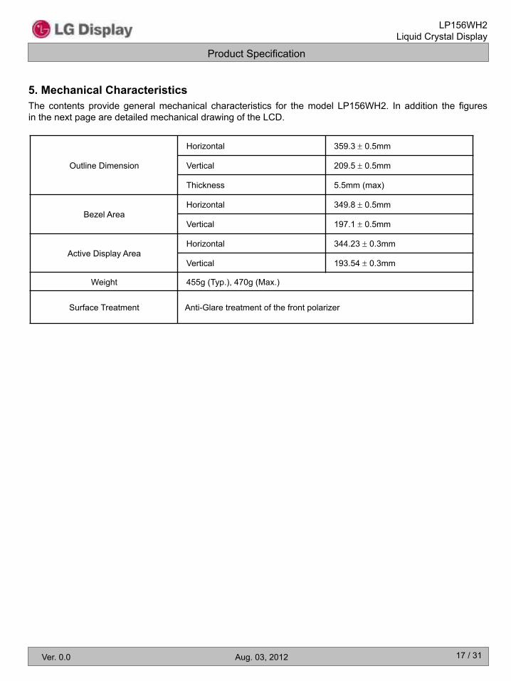
5. Mechanical Characteristics The contents provide general mechanical characteristics for the model LP156WH2. In addition the figures in the next page are detailed mechanical drawing of the LCD.
Outline Dimension
Horizontal 359.3 ± 0.5mm
Vertical 209.5 ± 0.5mm
Thickness 5.5mm (max)
Bezel Area Horizontal 349.8 ± 0.5mm
Vertical 197.1 ± 0.5mm
Active Display Area Horizontal 344.23 ± 0.3mm
Vertical 193.54 ± 0.3mm
Weight 455g (Typ.), 470g (Max.)
Surface Treatment Anti-Glare treatment of the front polarizer

Product Specification
LP156WH2 Liquid Crystal Display
Ver. 0.0 Aug. 03, 2012 18 / 31
<FRONT VIEW> Note) Unit:[mm], General tolerance: ± 0.5mm
This panel is symmetric

Product Specification
LP156WH2 Liquid Crystal Display
Ver. 0.0 Aug. 03, 2012 19 / 31
<REAR VIEW> Note) Unit:[mm], General tolerance: ± 0.5mm

Product Specification
LP156WH2 Liquid Crystal Display
Ver. 0.0 Aug. 03, 2012 20 / 31
[ DETAIL DESCRIPTION OF SIDE MOUNTING SCREW ]
* Mounting Screw Length (A) = 2.0(Min) / 2.5(Max) * Mounting Screw Hole Depth (B) = 2.5(Min) * Mounting hole location : 3.1(Typ) * Torque : 2.0 kgf.cm(Max) (Measurement gauge : torque meter)
Notes : 1. Screw plated through the method of non-electrolytic nickel plating is preferred to reduce possibility that results in vertical and/or horizontal line defect due to the conductive particles from screw surface.
※M2 : Screw Diameter =2.0mm
Product Specification
LP156WH2 Liquid Crystal Display
Ver. 0.0 Aug. 03, 2012 21 / 31
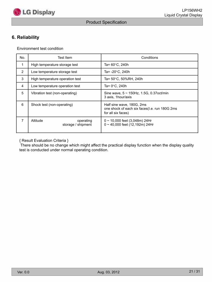
6. Reliability
Environment test condition
{ Result Evaluation Criteria } There should be no change which might affect the practical display function when the display quality test is conducted under normal operating condition.
No. Test Item Conditions
1 High temperature storage test Ta= 60°C, 240h
2 Low temperature storage test Ta= -20°C, 240h
3 High temperature operation test Ta= 50°C, 50%RH, 240h
4 Low temperature operation test Ta= 0°C, 240h
5 Vibration test (non-operating) Sine wave, 5 ~ 150Hz, 1.5G, 0.37oct/min 3 axis, 1hour/axis
6 Shock test (non-operating) Half sine wave, 180G, 2ms one shock of each six faces(I.e. run 180G 2ms for all six faces)
7 Altitude operating storage / shipment
0 ~ 10,000 feet (3,048m) 24Hr 0 ~ 40,000 feet (12,192m) 24Hr

Product Specification
LP156WH2 Liquid Crystal Display
Ver. 0.0 Aug. 03, 2012 22 / 31
7. International Standards
7-1. Safety
c) EN 60950-1:2006 + A11:2009, European Committee for Electrotechnical Standardization (CENELEC). Information Technology Equipment - Safety - Part 1 : General Requirements.
a) UL 60950-1, Second Edition, Underwriters Laboratories Inc. Information Technology Equipment - Safety - Part 1 : General Requirements. b) CAN/CSA C22.2 No.60950-1-07, Second Edition, Canadian Standards Association. Information Technology Equipment - Safety - Part 1 : General Requirements.
d) IEC 60950-1:2005, Second Edition, The International Electrotechnical Commission (IEC). Information Technology Equipment - Safety - Part 1 : General Requirements.
7-3. Environment
a) RoHS, Directive 2002/95/EC of the European Parliament and of the council of 27 January 2003
7-2. EMC
a) ANSI C63.4 “American National Standard for Methods of Measurement of Radio-Noise Emissions from Low-Voltage Electrical and Electronic Equipment in the Range of 9 kHz to 40 GHz.” American National Standards Institute (ANSI), 2003.
b) CISPR 22 “Information technology equipment – Radio disturbance characteristics – Limit and methods of measurement." International Special Committee on Radio Interference (CISPR), 2005.
c) CISPR 13 “Sound and television broadcast receivers and associated equipment – Radio disturbance characteristics – Limits and method of measurement." International Special Committee on Radio Interference (CISPR), 2006.

Product Specification
LP156WH2 Liquid Crystal Display
Ver. 0.0 Aug. 03, 2012 23 / 31
8. Packing
8-2. Packing Form
a) Package quantity in one box : 22 pcs b) Box Size :478 x 365 x 288
8-1. Designation of Lot Mark a) Lot Mark
A B C D E F G H I J K L M
A,B,C : SIZE(INCH) D : YEAR E : MONTH F ~ M : SERIAL NO.
Note 1. YEAR
2. MONTH
B
Nov
Mark
Month
A
Oct
6
Jun
7
Jul
8
Aug
9
Sep
4
Apr
5
May
C 3 2 1
Dec Mar Feb Jan
b) Location of Lot Mark
Serial No. is printed on the label. The label is attached to the backside of the LCD module. This is subject to change without prior notice.
Mark
Year
K
2020
F
2016
G
2017
H
2018
J
2019
D
2014
E
2015
C B A
2013 2012 2011
LGD Lot Mark

Product Specification
LP156WH2 Liquid Crystal Display
Ver. 0.0 Aug. 03, 2012 24 / 31
# APPENDIX-1 ■ Box Label
■ Pallet Label
LGD Lot Mark
Quantity
Shipping date
(12-30 : 月–日)
LGD Lot Mark
Quantity
Shipping date
(12-30 : 月–日)

Product Specification
LP156WH2 Liquid Crystal Display
Ver. 0.0 Aug. 03, 2012 25 / 31
# APPENDIX-2 ■ Packing Assembly
NO. DESCRIPTION MATERIAL
1 LCD Module
2 BAG LDPE
3 TAPE MASKING 20MMX50M
4 PACKING, TOP EPS
5 PACKING, BOTTOM EPS
6 BOX SWR4
7 TAPE OPP 70MMX300M
8 LABEL ART 100X70
④
⑤
⑥
①
②
③
1 LCM / 1 Bag
22LCM/Box = 11 Slot
2 LCM / 1 Slot

Product Specification
LP156WH2 Liquid Crystal Display
Ver. 0.0 Aug. 03, 2012 26 / 31
# APPENDIX-3 ■ Pallet Assembly
NO. DESCRIPTION MATERIAL
1 Packing AssY
2 Pallet Plywood
3 Angle Cover SWR4
4 Label ART 100X70
5 Band PP
6 Wrap LLDPE
7 CLIP Steel
①
②
⑤ ③
④
⑦
⑥

Product Specification
LP156WH2 Liquid Crystal Display
Ver. 0.0 Aug. 03, 2012 27 / 31
9. PRECAUTIONS
Please pay attention to the followings when you use this TFT LCD module.
9-1. MOUNTING PRECAUTIONS (1) You must mount a module using holes arranged in four corners or four sides. (2) You should consider the mounting structure so that uneven force (ex. Twisted stress) is not applied to th
e module. And the case on which a module is mounted should have sufficient strength so that external
force is not transmitted directly to the module. (3) Please attach the surface transparent protective plate to the surface in order to protect the polarizer. Transparent protective plate should have sufficient strength in order to the resist external force. (4) You should adopt radiation structure to satisfy the temperature specification. (5) Acetic acid type and chlorine type materials for the cover case are not desirable because the former generates corrosive gas of attacking the polarizer at high temperature and the latter causes circuit break
by electro-chemical reaction. (6) Do not touch, push or rub the exposed polarizers with glass, tweezers or anything harder than HB pencil lead. And please do not rub with dust clothes with chemical treatment. Do not touch the surface of polarizer for bare hand or greasy cloth.(Some cosmetics are detrimental to the polarizer.) (7) When the surface becomes dusty, please wipe gently with absorbent cotton or other soft materials like
chamois soaks with petroleum benzene. Normal-hexane is recommended for cleaning the adhesives used to attach front / rear polarizers. Do not use acetone, toluene and alcohol because they cause chemical damage to the polarizer.
(8) Wipe off saliva or water drops as soon as possible. Their long time contact with polarizer causes deformations and color fading.
(9) Do not open the case because inside circuits do not have sufficient strength.
9-2. OPERATING PRECAUTIONS
(1) The spike noise causes the mis-operation of circuits. It should be lower than following voltage : V=± 200mV(Over and under shoot voltage)
(2) Response time depends on the temperature.(In lower temperature, it becomes longer.) (3) Brightness depends on the temperature. (In lower temperature, it becomes lower.) And in lower temperature, response time(required time that brightness is stable after turned on) becomes longer. (4) Be careful for condensation at sudden temperature change. Condensation makes damage to polarizer or
electrical contacted parts. And after fading condensation, smear or spot will occur. (5) When fixed patterns are displayed for a long time, remnant image is likely to occur. (6) Module has high frequency circuits. Sufficient suppression to the electromagnetic interference shall be
done by system manufacturers. Grounding and shielding methods may be important to minimized the interference.

Product Specification
LP156WH2 Liquid Crystal Display
Ver. 0.0 Aug. 03, 2012 28 / 31
Since a module is composed of electronic circuits, it is not strong to electrostatic discharge. Make certain that treatment persons are connected to ground through wrist band etc. And don’t touch interface pin directly.
9-3. ELECTROSTATIC DISCHARGE CONTROL
Strong light exposure causes degradation of polarizer and color filter.
9-4. PRECAUTIONS FOR STRONG LIGHT EXPOSURE
9-5. STORAGE
(1) When the protection film is peeled off, static electricity is generated between the film and polarizer. This should be peeled off slowly and carefully by people who are electrically grounded and with well ion-blown equipment or in such a condition, etc. (2) The protection film is attached to the polarizer with a small amount of glue. If some stress is applied to rub the protection film against the polarizer during the time you peel off the film, the glue is apt to remain on the polarizer. Please carefully peel off the protection film without rubbing it against the polarizer. (3) When the module with protection film attached is stored for a long time, sometimes there remains a very small amount of glue still on the polarizer after the protection film is peeled off. (4) You can remove the glue easily. When the glue remains on the polarizer surface or its vestige is recognized, please wipe them off with absorbent cotton waste or other soft material like chamois soaked with normal-hexane.
9-6. HANDLING PRECAUTIONS FOR PROTECTION FILM
When storing modules as spares for a long time, the following precautions are necessary. (1) Store them in a dark place. Do not expose the module to sunlight or fluorescent light. Keep the
temperature between 5°C and 35°C at normal humidity. (2) The polarizer surface should not come in contact with any other object. It is recommended that they be stored in the container in which they were shipped.
Product Specification
LP156WH2 Liquid Crystal Display
Ver. 0.0 Aug. 03, 2012 29 / 31
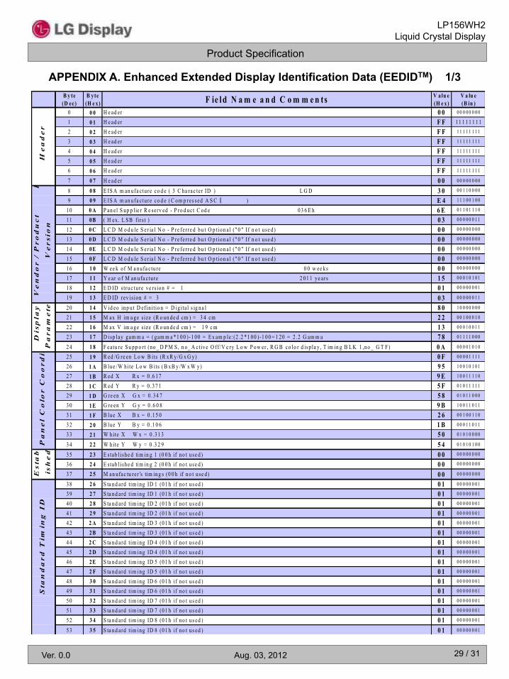
APPENDIX A. Enhanced Extended Display Identification Data (EEDIDTM) 1/3 B y te(D ec)
B yte(H e x) F ie ld N a m e a n d C o m m e n ts V alu e
(H e x)V a lu e(B in )
0 0 0 H e ad er 0 0 0 0 0 0 0 0 0 0
1 0 1 H e ad er F F 11 1 11 1 11
2 0 2 H e ad er F F 1 1 1 1 1 1 1 1
3 0 3 H e ad er F F 1 1 1 1 1 1 1 1
4 0 4 H e ad er F F 1 1 1 1 1 1 1 1
5 0 5 H e ad er F F 1 1 1 1 1 1 1 1
6 0 6 H e ad er F F 1 1 1 1 1 1 1 1
7 0 7 H e ad er 0 0 0 0 0 0 0 0 0 0
8 0 8 E IS A m an ufa c tu re co d e ( 3 C ha rac te r ID ) L G D 3 0 0 0 1 1 0 0 0 0
9 0 9 E IS A m an ufa c tu re co d e ( C om p res sed A S CⅡ ) E 4 1 1 1 0 0 1 0 0
10 0 A P an e l S up p lie r R e se rv ed - P ro d uc t C od e 03 6 E h 6 E 0 1 1 0 1 1 1 0
11 0B ( H ex . L S B f irs t ) 0 3 0 0 0 0 0 0 1 1
12 0 C L C D M o du le S er ia l N o - P re fe rre d bu t O p tion a l (" 0 " I f n o t u se d ) 0 0 0 0 0 0 0 0 0 0
13 0 D L C D M o du le S er ia l N o - P re fe rre d bu t O p tion a l (" 0 " I f n o t u se d ) 0 0 0 0 0 0 0 0 0 0
14 0E L C D M o du le S er ia l N o - P re fe rre d bu t O p tion a l (" 0 " I f n o t u se d ) 0 0 0 0 0 0 0 0 0 0
15 0 F L C D M o du le S er ia l N o - P re fe rre d bu t O p tion a l (" 0 " I f n o t u se d ) 0 0 0 0 0 0 0 0 0 0
16 1 0 W ee k o f M a nufa c tu re 0 0 w ee ks 0 0 0 0 0 0 0 0 0 0
17 1 1 Y e ar o f M an ufa c tu re 2 01 1 ye ars 1 5 0 0 0 1 0 1 0 1
18 1 2 E D ID s truc tu re ve rs ion # = 1 0 1 0 0 0 0 0 0 0 1
19 1 3 E D ID rev is ion # = 3 0 3 0 0 0 0 0 0 1 1
20 1 4 V id eo inp u t D ef in i t io n = D ig ita l s ig na l 8 0 1 0 0 0 0 0 0 0
21 1 5 M ax H im a ge s ize (R o un de d cm ) = 3 4 cm 2 2 0 0 1 0 0 0 1 0
22 1 6 M ax V im a ge s ize (R o un de d cm ) = 1 9 c m 1 3 0 0 0 1 0 0 1 1
23 1 7 D isp lay gam m a = ( gam m a *1 00 )-1 00 = E x am p le :(2 .2 *1 00 )-1 00 = 1 20 = 2 .2 G am m a 7 8 0 1 1 1 1 0 0 0
24 1 8 F ea tu re S u pp o rt (no _ D P M S , n o_ A ctive O ff /V e ry L o w P ow er , R G B co lo r d isp la y , T im in g B L K 1 ,no _ G T F ) 0 A 0 0 0 0 1 0 1 0
25 1 9 R ed /G re en L o w B its (R xR y /G x G y) 0 F 0 0 0 0 1 1 1 1
26 1 A B lue /W hite L o w B its ( B xB y /W x W y) 9 5 1 0 0 1 0 1 0 1
27 1B R ed X R x = 0 .6 17 9 E 1 0 0 1 1 1 1 0
28 1 C R ed Y R y = 0 .37 1 5 F 0 1 0 1 1 1 1 1
29 1 D G re en X G x = 0 .34 7 5 8 0 1 0 1 1 0 0 0
30 1E G re en Y G y = 0 .6 0 8 9 B 1 0 0 1 1 0 1 1
31 1 F B lue X B x = 0 .15 0 2 6 0 0 1 0 0 1 1 0
32 2 0 B lue Y B y = 0 .1 0 6 1 B 0 0 0 1 1 0 1 1
33 2 1 W hite X W x = 0 .31 3 5 0 0 1 0 1 0 0 0 0
34 2 2 W hite Y W y = 0 .3 2 9 5 4 0 1 0 1 0 1 0 0
35 2 3 E stab lishe d tim in g 1 (0 0 h if no t u se d ) 0 0 0 0 0 0 0 0 0 0
36 2 4 E stab lishe d tim in g 2 (0 0 h if no t u se d ) 0 0 0 0 0 0 0 0 0 0
37 2 5 M an ufac tu re r 's tim ing s (0 0 h if no t u se d ) 0 0 0 0 0 0 0 0 0 0
38 2 6 S ta nd ard t im ing ID 1 (01 h if no t u s ed ) 0 1 0 0 0 0 0 0 0 1
39 2 7 S ta nd ard t im ing ID 1 (01 h if no t u s ed ) 0 1 0 0 0 0 0 0 0 1
40 2 8 S ta nd ard t im ing ID 2 (01 h if no t u s ed ) 0 1 0 0 0 0 0 0 0 1
41 2 9 S ta nd ard t im ing ID 2 (01 h if no t u s ed ) 0 1 0 0 0 0 0 0 0 1
42 2 A S ta nd ard t im ing ID 3 (01 h if no t u s ed ) 0 1 0 0 0 0 0 0 0 1
43 2B S ta nd ard t im ing ID 3 (01 h if no t u s ed ) 0 1 0 0 0 0 0 0 0 1
44 2 C S ta nd ard t im ing ID 4 (01 h if no t u s ed ) 0 1 0 0 0 0 0 0 0 1
45 2 D S ta nd ard t im ing ID 4 (01 h if no t u s ed ) 0 1 0 0 0 0 0 0 0 1
46 2E S ta nd ard t im ing ID 5 (01 h if no t u s ed ) 0 1 0 0 0 0 0 0 0 1
47 2 F S ta nd ard t im ing ID 5 (01 h if no t u s ed ) 0 1 0 0 0 0 0 0 0 1
48 3 0 S ta nd ard t im ing ID 6 (01 h if no t u s ed ) 0 1 0 0 0 0 0 0 0 1
49 3 1 S ta nd ard t im ing ID 6 (01 h if no t u s ed ) 0 1 0 0 0 0 0 0 0 1
50 3 2 S ta nd ard t im ing ID 7 (01 h if no t u s ed ) 0 1 0 0 0 0 0 0 0 1
51 3 3 S ta nd ard t im ing ID 7 (01 h if no t u s ed ) 0 1 0 0 0 0 0 0 0 1
52 3 4 S ta nd ard t im ing ID 8 (01 h if no t u s ed ) 0 1 0 0 0 0 0 0 0 1
53 3 5 S ta nd ard t im ing ID 8 (01 h if no t u s ed ) 0 1 0 0 0 0 0 0 0 1
Es
tab
l
ish
ed
Sta
nd
ar
d T
imin
g I
DH
ea
de
rV
en
do
r /
Pr
od
uc
t
E
DI
D
Ve
rsio
n
Dis
pla
y
Pa
ra
me
ters
Pa
ne
l C
olo
r C
oo
rd
ina
tes
Product Specification
LP156WH2 Liquid Crystal Display
Ver. 0.0 Aug. 03, 2012 30 / 31
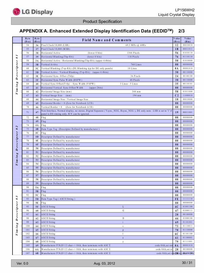
APPENDIX A. Enhanced Extended Display Identification Data (EEDIDTM) 2/3 B y te(D ec)
B yte(H e x) F ie ld N a m e a n d C o m m e n ts V alu e
(H e x)V a lu e(B in )
54 3 6 P ixe l C loc k /1 0 ,00 0 (L S B ) 6 9 .3 M H z @ 6 0H z 1 2 0 0 0 1 0 0 1 0
55 3 7 P ixe l C loc k /1 0 ,00 0 (M S B ) 1 B 0 0 0 1 1 0 1 1
56 3 8 H o rizo n ta l A c tive ( lo w er 8 b i ts ) 13 6 6 P ix e ls 5 6 0 1 0 1 0 1 1 0
57 3 9 H o rizo n ta l B lan k ing (T hp -H A ) ( lo w e r 8 b i ts ) 1 18 P ixe ls 7 6 0 1 1 1 0 1 1 0
58 3 A H o rizo n ta l A c tive / H o rizo n ta l B lan k ing (T h p-H A ) (up p er 4 :4 b its ) 5 0 0 1 0 1 0 0 0 0
59 3B V e rtic a l A v tiv e 76 8 L ine s 0 0 0 0 0 0 0 0 0 0
60 3 C V e rtic a l B la nk in g (T vp -H A ) (D E B la nk in g ty p . fo r D E o n ly pa ne ls ) 1 0 L in es 0 A 0 0 0 0 1 0 1 0
61 3 D V e rtic a l A c tiv e : V er tic a l B la nk in g (T vp -H A ) ( up pe r 4 :4b its ) 3 0 0 0 1 1 0 0 0 0
62 3E H o rizo n ta l S y nc . O ffse t (T h fp ) 3 6 P ixe ls 2 4 0 0 1 0 0 1 0 0
63 3 F H o rizo n ta l S y nc P u lse W id th (H S P W ) 4 8 P ix e ls 3 0 0 0 1 1 0 0 0 0
64 4 0 V e rtic a l S yn c O ffse t(T v fp ) : S ync W id th (V S P W ) 3 L in es : 5 L in es 3 5 0 0 1 1 0 1 0 1
65 4 1 H o rizo n ta l V er t ic a l S yn c O ffs e t /W id th (up pe r 2 b its ) 0 0 0 0 0 0 0 0 0 0
66 4 2 H o rizo n ta l Im ag e S ize (m m ) 3 4 4 m m 5 8 0 1 0 1 1 0 0 0
67 4 3 V e rtic a l Im a ge S ize (m m ) 19 4 m m C 2 1 1 0 0 0 0 1 0
68 4 4 H o rizo n ta l Im ag e S ize / V e r t ica l Im ag e S ize 1 0 0 0 0 1 0 0 0 0
69 4 5 H o rizo n ta l B o rde r = 0 (Z e ro fo r N o teb oo k L C D ) 0 0 0 0 0 0 0 0 0 0
70 4 6 V e rtic a l B o rd er = 0 (Z e ro fo r N o teb oo k L C D ) 0 0 0 0 0 0 0 0 0 0
71 4 7N o n-In te r lac e , N o rm al d isp la y , no s te reo , D ig ita l S ep ara te ( V syn c_ N E G , H sy nc_ N E G ) , D E o n ly no te : L S B is se t to '1 ' i fp ane l is D E -tim ing o n ly . H /V c an b e ig no red .
1 9 0 0 0 1 1 0 0 1
72 4 8 F la g 0 0 0 0 0 0 0 0 0 0
73 4 9 F la g 0 0 0 0 0 0 0 0 0 0
74 4 A F la g 0 0 0 0 0 0 0 0 0 0
75 4B D a ta T y pe T a g (D es c r ip to r D ef ine d by m an ufac tu re r ) 0 0 0 0 0 0 0 0 0 0
76 4 C F la g 0 0 0 0 0 0 0 0 0 0
77 4 D D e scr ip to r D ef ine d b y m an ufa c tu re r 0 0 0 0 0 0 0 0 0 0
78 4E D e scr ip to r D ef ine d b y m an ufa c tu re r 0 0 0 0 0 0 0 0 0 0
79 4 F D e scr ip to r D ef ine d b y m an ufa c tu re r 0 0 0 0 0 0 0 0 0 0
80 5 0 D e scr ip to r D ef ine d b y m an ufa c tu re r 0 0 0 0 0 0 0 0 0 0
81 5 1 D e scr ip to r D ef ine d b y m an ufa c tu re r 0 0 0 0 0 0 0 0 0 0
82 5 2 D e scr ip to r D ef ine d b y m an ufa c tu re r 0 0 0 0 0 0 0 0 0 0
83 5 3 D e scr ip to r D ef ine d b y m an ufa c tu re r 0 0 0 0 0 0 0 0 0 0
84 5 4 D e scr ip to r D ef ine d b y m an ufa c tu re r 0 0 0 0 0 0 0 0 0 0
85 5 5 D e scr ip to r D ef ine d b y m an ufa c tu re r 0 0 0 0 0 0 0 0 0 0
86 5 6 D e scr ip to r D ef ine d b y m an ufa c tu re r 0 0 0 0 0 0 0 0 0 0
87 5 7 D e scr ip to r D ef ine d b y m an ufa c tu re r 0 0 0 0 0 0 0 0 0 0
88 5 8 D e scr ip to r D ef ine d b y m an ufa c tu re r 0 0 0 0 0 0 0 0 0 0
89 5 9 D e scr ip to r D ef ine d b y m an ufa c tu re r 0 0 0 0 0 0 0 0 0 0
90 5 A F la g 0 0 0 0 0 0 0 0 0 0
91 5B F la g 0 0 0 0 0 0 0 0 0 0
92 5 C F la g 0 0 0 0 0 0 0 0 0 0
93 5 D D a ta T y pe T a g ( A S C I I S tr in g ) F E 1 1 1 1 1 1 1 0
94 5E F la g 0 0 0 0 0 0 0 0 0 0
95 5 F A S C II S tr ing L 4 C 0 1 0 0 1 1 0 0
96 6 0 A S C II S tr ing G 4 7 0 1 0 0 0 1 1 1
97 6 1 A S C II S tr ing 2 0 0 0 1 0 0 0 0 0
98 6 2 A S C II S tr ing D 4 4 0 1 0 0 0 1 0 0
99 6 3 A S C II S tr ing i 6 9 0 1 1 0 1 0 0 1
1 0 0 6 4 A S C II S tr ing s 7 3 0 1 1 1 0 0 1 1
1 0 1 6 5 A S C II S tr ing p 7 0 0 1 1 1 0 0 0 0
1 0 2 6 6 A S C II S tr ing l 6 C 0 1 1 0 1 1 0 0
1 0 3 6 7 A S C II S tr ing a 6 1 0 1 1 0 0 0 0 1
1 0 4 6 8 A S C II S tr ing y 7 9 0 1 1 1 1 0 0 1
1 0 5 6 9 M an ufac tu re r P /N (If< 1 3 cha r--> 0 A h , th en te rm in a te w ith A S CⅡ c od e 0 A h ,se t rem a in ing c har = 2 0h ) 0 A 0 0 0 0 1 0 1 0
1 0 6 6 A M an ufac tu re r P /N (If< 1 3 cha r--> 0 A h , th en te rm in a te w ith A S CⅡ co de 0 A h , se t re m ain in g cha r = 2 0 h ) 2 0 0 0 1 0 0 0 0 0
1 0 7 6B M an ufac tu re r P /N (If< 1 3 cha r--> 0 A h , th en te rm in a te w ith A S CⅡ co d e 0A h ,se t rem a in ing ch ar = 20 h )2 0 0 0 1 0 0 0 0 0
Tim
ing
De
sc
rip
tor #
3T
imin
g D
es
cr
ipto
r #
1T
imin
g D
es
cr
ipto
r #
2
Product Specification
LP156WH2 Liquid Crystal Display
Ver. 0.0 Aug. 03, 2012 31 / 31
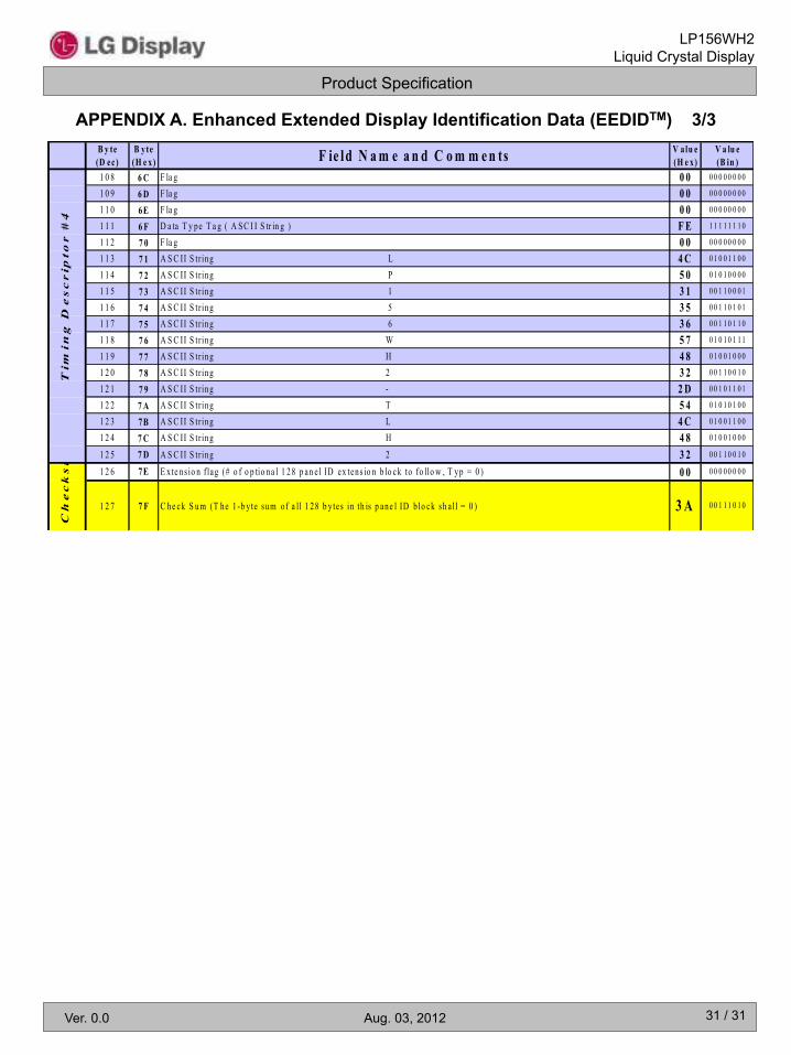
APPENDIX A. Enhanced Extended Display Identification Data (EEDIDTM) 3/3 B y te
(D ec)B yte
(H e x) F ie ld N a m e a n d C o m m e n ts V alu e(H e x)
V a lu e(B in )
1 0 8 6 C F la g 0 0 0 0 0 0 0 0 0 0
1 0 9 6 D F la g 0 0 0 0 0 0 0 0 0 0
1 1 0 6E F la g 0 0 0 0 0 0 0 0 0 0
1 1 1 6 F D a ta T y pe T a g ( A S C I I S tr in g ) F E 1 1 1 1 1 1 1 0
1 1 2 7 0 F la g 0 0 0 0 0 0 0 0 0 0
1 1 3 7 1 A S C II S tr ing L 4 C 0 1 0 0 1 1 0 0
1 1 4 7 2 A S C II S tr ing P 5 0 0 1 0 1 0 0 0 0
1 1 5 7 3 A S C II S tr ing 1 3 1 0 0 1 1 0 0 0 1
1 1 6 7 4 A S C II S tr ing 5 3 5 0 0 1 1 0 1 0 1
1 1 7 7 5 A S C II S tr ing 6 3 6 0 0 1 1 0 1 1 0
1 1 8 7 6 A S C II S tr ing W 5 7 0 1 0 1 0 1 1 1
1 1 9 7 7 A S C II S tr ing H 4 8 0 1 0 0 1 0 0 0
1 2 0 7 8 A S C II S tr ing 2 3 2 0 0 1 1 0 0 1 0
1 2 1 7 9 A S C II S tr ing - 2 D 0 0 1 0 1 1 0 1
1 2 2 7 A A S C II S tr ing T 5 4 0 1 0 1 0 1 0 0
1 2 3 7B A S C II S tr ing L 4 C 0 1 0 0 1 1 0 0
1 2 4 7 C A S C II S tr ing H 4 8 0 1 0 0 1 0 0 0
1 2 5 7 D A S C II S tr ing 2 3 2 0 0 1 1 0 0 1 0
1 2 6 7E E xte ns io n f lag (# o f o p tio na l 1 28 p an e l ID ex tens io n b lo ck to fo llo w , T yp = 0 ) 0 0 0 0 0 0 0 0 0 0
1 2 7 7 F C he ck S um (T he 1 -b y te sum o f a l l 1 28 b y tes in th is p ane l ID b lo ck sh a ll = 0 ) 3 A 0 0 1 1 1 0 1 0
Tim
ing
De
sc
rip
tor #
4C
he
ck
su
m

AvnET EmBEddEd officES
dEnmArkAvnet EmbeddedAvnet Nortec A/SEllekær 92730 HerlevPhone: +45 3678 6250Fax: +45 3678 [email protected]
finlAndAvnet EmbeddedAvnet Nortec OyPihatörmä 1 B02240 EspooPhone: +358 20 749 9 260Fax: +358 20 749 9 [email protected]
frAncEAvnet EmbeddedAvnet EMG France SAParc Club du Moulin à Vent, Bât 1033, rue du Dr Georges Lévy 69693 Vénissieux CedexPhone: +33 4 78 77 13 92Fax: +33 4 78 77 13 [email protected]
Avnet EmbeddedAvnet EMG France SA14 avenue Carnot 91349 Massy Cedex Phone: +33 1 64 47 29 29Fax: +33 1 64 47 99 [email protected]
Avnet EmbeddedAvnet EMG France SALes Peupliers II35 avenue des Peupliers35510 Cesson-SévignéPhone: + 33 2 99 77 37 02Fax: + 33 2 99 77 37 [email protected]
GErmAnY (AUSTriA, cZEcH rEpUBlic, HUnGArY, polAnd, SWiTZErlAnd)Avnet EmbeddedAvnet EMG GmbHGruber Straße 60c85586 PoingPhone: +49 8121 775 500 Fax: +49 8121 775 [email protected]
Avnet EmbeddedAvnet EMG GmbHLötscher Weg 6641334 NettetalPhone: +49 8121 775 500Fax: +49 8121 775 [email protected]
iTAlY (porTUGAl, SpAin)Avnet EmbeddedAvnet EMG Italy SRLVia Manzoni, 4420095 Cusano MilaninoPhone: +39 02 660 92 1Fax: +39 02 660 92 [email protected]
nETHErlAndS (BElGiUm, lUXEmBoUrG)Avnet EmbeddedAvnet B.V.Takkebijsters 24817 BL BredaPhone: +31 76 5722400Fax: +31 76 [email protected]
SWEdEn (norWAY)Avnet EmbeddedAvnet Nortec ABEsplanaden 3 D172 67 SundbybergPhone: +46 8 564 725 50Fax: +46 8 760 01 [email protected]
UniTEd kinGdom (irElAnd)Avnet Embedded5a Waltham ParkWhite WalthamMaidenheadBerkshire, SL6 3TNPhone: +44 1628 518900Fax: +44 1628 [email protected]
www.avnet-embedded.eu
02/2013
All trademarks and logos are the property of their respective owners. No guarentee as to the accuracy, completeness or reliability of any information. Subject to modifications and amendments.