southern island architecture
TRANSCRIPT

12/23/11 AnandTech.com - AMD's Graphics Core Next Preview: AMD's New GPU, …
1/12www.anandtech.com/print/4455
AMD's Graphics Core Next Preview: AMD's New GPU, Architected For Computeby Ryan Smith on 12/21/2011 9:38:00 PM
Posted in GPUs , AMD , GCN , Radeon
Update: This article was originally posted on June 17, 2011. We are pushing it back up to the top as a quick refresherbefore upcoming articles...
We’ve just returned from sunny Bellevue, Washington, where AMD held their first Fusion Developer Summit (AFDS). As withother technical conferences of this nature such as NVIDIA’s GTC and Intel’s IDF, AFDS is a chance for AMD to reach out todevelopers to prepare them for future products and to receive feedback in turn. While AMD can make powerful hardware it’sultimately the software that runs on it that drives sales, so it’s important for them to reach out to developers to ensure that suchsoftware is being made.
While AFDS serves many purposes, the final purpose – and what is going to be most interesting to most outside observers –was to prepare developers for what’s coming down the pipe. AMD has big plans for the future and it’s important to getdevelopers involved as soon as is reasonably possible so that they’re ready to use AMD’s future technologies when theylaunch. Over the next few days we’ll talk about a couple of different things AMD is working on, and today we’ll start with the firstand most exciting project: AMD Graphics Core Next, AMD's next generation GPU architecture.
Page 1
We’ve just returned from sunny Bellevue, Washington, where AMD held their first Fusion Developer Summit (AFDS). As withother technical conferences of this nature such as NVIDIA’s GTC and Intel’s IDF, AFDS is a chance for AMD to reach out todevelopers to prepare them for future products and to receive feedback in turn. While AMD can make powerful hardware it’sultimately the software that runs on it that drives sales, so it’s important for them to reach out to developers to ensure that suchsoftware is being made.
AFDS 2011 served as a focal point for several different things going on at AMD. At its broadest, it was a launch event forLlano, AMD’s first mainstream Fusion APU that launched at the start of the week. AMD has invested the future of the companyinto APUs, and not just for graphical purposes but for compute purposes too. So Llano is a big deal for the company eventhough it’s only a taste of what’s to come.
The second purpose of course was to provide sessions for developers to learn more about how to utilize AMD’s GPUs forcompute and graphics tasks. Microsoft, Acceleware, Adobe, academic researchers, and others were on hand to providetalks on how they’re using GPUs in current and future projects.
The final purpose – and what is going to be most interesting to most outside observers – was to prepare developers forwhat’s coming down the pipe. AMD has big plans for the future and it’s important to get developers involved as soon as is

12/23/11 AnandTech.com - AMD's Graphics Core Next Preview: AMD's New GPU, …
2/12www.anandtech.com/print/4455
reasonably possible so that they’re ready to use AMD’s future technologies when they launch. Over the next few days we’ll talkabout a couple of different things AMD is working on, and today we’ll start with the first and most exciting project: AMDGraphics Core Next.
Graphics Core Next (GCN) is the architectural basis for AMD’s future GPUs, both for discrete products and for GPUsintegrated with CPUs as part of AMD’s APU products. AMD will be instituting a major overhaul of its traditional GPUarchitecture for future generation products in order to meet the direction of the market and where they want to go with theirGPUs in the future.
While graphics performance and features have been and will continue to be important aspects of a GPU’s design, AMD andthe rest of the market have been moving towards further exploiting the compute capabilities of GPUs, which in the rightcircumstances are capable of being utilized as massive parallel processors that can complete a number of tasks in thefraction of the time as a highly generalized CPU. Since the introduction of shader-capable GPUs in 2002, GPUs have slowlyevolved to become more generalized so that their resources can be used for more than just graphics. AMD’s most recent shiftwas with their VLIW4 architecture with Cayman late last year; now they’re looking to make their biggest leap yet with GCN.
GCN at its core is the basis of a GPU that performs well at both graphical and computing tasks. AMD has stretched theirtraditional VLIW architecture as far as they reasonably can for computing purposes, and as more developers get on board forGPU computing a clean break is needed in order to build a better performing GPU to meet their needs. This is in essenceAMD’s Fermi: a new architecture and a radical overhaul to make a GPU that is as monstrous at computing as it is atgraphics. And this is the story of the architecture that AMD will be building to make it happen.
Finally, it should be noted that the theme of AFDS 2011 was heterogeneous computing, as it has become AMD’s focus to getdevelopers to develop heterogeneous applications that effectively utilize both AMD’s CPUs and AMD’s GPUs. OstensiblyAFDS is a conference about GPU computing, but AMD’s true strength is not their CPU side or their GPU side, it’s thecombination of the two. Bulldozer will be the first half of AMD’s future APUs, while GCN will be the other half.
Page 2
Prelude: The History of VLIW & Graphics
Before we get into the nuts & bolts of Graphics Core Next, perhaps it’s best to start at the bottom, and then work our way up.
The fundamental unit of AMD’s previous designs has been the Streaming Processor, previously known as the SPU. In everymodern AMD design other than Cayman (6900), this is a Very Long Instruction Word 5 (VLIW5) design; Cayman reduced thisto VLIW4. As implied by the architectural name, each SP would in turn have 5 or 4 fundamental math units – what AMD nowcalls Radeon cores – which executed the individual instructions in parallel over as many clocks as necessary. Radeon coreswere coupled with registers, a branch unit, and a special function (transcendental) unit as necessary to complete the SP.
VLIW designs are designed to excel at executing many operations from the same task in parallel by breaking it up intosmaller groupings called wavefronts. In AMD’s case a wavefront is a group of 64 pixels/values and the list of instructions to beexecuted against them. Ideally, in a wavefront a group of 4 or 5 instructions will come down the pipe and be completely non-interdependent, allowing every Radeon core to be fed. When dependent instructions would come down however, fewerinstructions could be scheduled at once, and in the worst case only a single instruction could be scheduled. VLIW designs willnever achieve perfect efficiency in this regard, but the farther real world utilization is from ideal efficiency, the weaker thebenefits of VLIW.

12/23/11 AnandTech.com - AMD's Graphics Core Next Preview: AMD's New GPU, …
3/12www.anandtech.com/print/4455
The use of VLIW can be traced back to the first AMD DX9 GPU, R300 (Radeon 9700 series). If you recall our Cayman launcharticle, we mentioned that AMD initially used a VLIW design in those early parts because it allowed them to process a 4component dot product (e.g. w, x, y, z) and a scalar component (e.g. lighting) at the same time, which was by far the mostcommon graphics operation. Even when moving to unified shaders in DX10 with R600 (Radeon HD 2900), AMD still kept theVLIW5 design because the gaming market was still DX9 and using those kinds of operations. But as new games andGPGPU programs have come out efficiency has dropped over time, and based on AMD’s own internal research at the time ofthe Cayman launch the average shader program was utilizing only 3.4 out of 5 Radeon cores. Shrinking from VLIW5 to VLIW4fights this some, but utilization will always be a concern.
Finally, it’s worth noting what’s in charge of doing all of the scheduling. In the CPU world we throw things at the CPU and let itschedule actions as necessary – it can even go out-of-order (OoO) within a thread if it will be worth it. With VLIW, schedulingis the domain of the compiler. The compiler gets the advantage of knowing about the full program ahead of time and canintelligently schedule some things well in advance, but at the same time it’s blind to other conditions where the outcome isunknown until the program is run and data is provided. Because of this the schedule is said to be static – it’s set at the time ofcompilation and cannot be changed in-flight.
So why in an article about AMD Graphics Core Next are we going over the quick history of AMD’s previous designs? Withoutunderstanding the previous designs, we can’t understand what is new about what AMD is doing, or more importantly whythey’re doing it.
Page 3
AMD Graphics Core Next: Out With VLIW, In With SIMD
The fundamental issue moving forward is that VLIW designs are great for graphics; they are not so great for computing.However AMD has for all intents and purposes bet the company on GPU computing – their Fusion initiative isn’t just aboutputting a decent GPU right on die with a CPU, but then utilizing the radically different design attributes of a GPU to do thecomputational work that the CPU struggles at. So a GPU design that is great at graphics and poor at computing work simplyisn’t sustainable for AMD’s future.
With AMD Graphics Core Next, VLIW is going away in favor of a non-VLIW SIMD design. In principal the two are similar – runlots of things in parallel – but there’s a world of difference in execution. Whereas VLIW is all about extracting instruction levelparallelism (ILP), a non-VLIW SIMD is primarily about thread level parallelism (TLP).
Without getting unnecessarily deep into the differences between VLIW and non-VLIW (we’ll save that for another time), thedifference in the architectures is about what VLIW does poorly for GPU computing purposes, and why a non-VLIW SIMD fixesit. The principal issue is that VLIW is hard to schedule ahead of time and there’s no dynamic scheduling during execution, andas a result the bulk of its weaknesses follow from that. As VLIW5 was a good fit for graphics, it was rather easy to efficientlycompile and schedule shaders under those circumstances. With compute this isn’t always the case; there’s simply a widerrange of things going on and it’s difficult to figure out what instructions will play nicely with each other. Only a handful of taskssuch as brute force hashing thrive under this architecture.

12/23/11 AnandTech.com - AMD's Graphics Core Next Preview: AMD's New GPU, …
4/12www.anandtech.com/print/4455
Furthermore as VLIW lives and dies by the compiler, which means not only must the compiler be good, but that everycompiler is good. This is an issue when it comes to expanding language support, as even with abstraction throughintermediate languages you can still run into issues, including issues with a compiler producing intermediate code that theshader compiler can’t handle well.
Finally, the complexity of a VLIW instruction set also rears its head when it comes to optimizing and hand-tuning a program.Again this isn’t normally a problem for graphics, but it is for compute. The complex nature of VLIW makes it harder todisassemble and to debug, and in turn difficult to predict performance and to find and fix performance critical sections of thecode. Ideally a coder should never have to work in assembly, but for HPC and other uses there is a good deal of performanceto be gained by doing so and optimizing down to the single instruction.
AMD provided a short example of this in their presentation, showcasing the example output of their VLIW compiler and theirnew compiler for Graphics Core Next. Being a coder helps, but it’s not hard to see how contrived things are under VLIW.
VLIW/ / R e g i s t e r s r 0 c o n t a i n s " a " , r 1 c o n t a i n s " b "/ / V a l u e i s r e t u r n e d i n r 20 0 A L U _ P U S H _ B E F O R E 1 x : P R E D G T _ _ _ _ , R 0 . x , R 1 . x U P D A T E _ E X E C _ M A S K U P D A T E P R E D0 1 J U M P A D D R ( 3 )0 2 A L U 2 x : S U B _ _ _ _ , R 0 . x , R 1 . x 3 x : M U L _ e R 2 . x , P V 2 . x , R 0 . x0 3 E L S E P O P _ C N T ( 1 ) A D D R ( 5 )0 4 A L U _ P O P _ A F T E R 4 x : S U B _ _ _ _ , R 1 . x , R 0 . x 5 x : M U L _ e R 2 . x , P V 4 . x , R 1 . x0 5 P O P ( 1 ) A D D R ( 6 )
Non-VLIW SIMD/ / R e g i s t e r s r 0 c o n t a i n s " a " , r 1 c o n t a i n s " b "/ / V a l u e i s r e t u r n e d i n r 2v _ c m p _ g t _ f 3 2 r 0 , r 1 / / a > b , e s t a b l i s h V C Cs _ m o v _ b 6 4 s 0 , e x e c / / S a v e c u r r e n t e x e c m a s ks _ a n d _ b 6 4 e x e c , v c c , e x e c / / D o " i f "s _ c b r a n c h _ v c c z l a b e l 0 / / B r a n c h i f a l l l a n e s f a i lv _ s u b _ f 3 2 r 2 , r 0 , r 1 / / r e s u l t = a - bv _ m u l _ f 3 2 r 2 , r 2 , r 0 / / r e s u l t = r e s u l t * a
s _ a n d n 2 _ b 6 4 e x e c , s 0 , e x e c / / D o " e l s e " ( s 0 & ! e x e c )s _ c b r a n c h _ e x e c z l a b e l 1 / / B r a n c h i f a l l l a n e s f a i lv _ s u b _ f 3 2 r 2 , r 1 , r 0 / / r e s u l t = b - av _ m u l _ f 3 2 r 2 , r 2 , r 1 / / r e s u l t = r e s u l t * b
s _ m o v _ b 6 4 e x e c , s 0 / / R e s t o r e e x e c m a s k
VLIW: it’s good for graphics, it’s often not as good for compute.
So what does AMD replace VLIW with? They replace it with a traditional SIMD vector processor. While elements of Caymando not directly map to elements of Graphics Core Next (GCN), since we’ve already been talking about the SP we’ll talk aboutits closest replacement: the SIMD.
Not to be confused with the SIMD on Cayman (which is a collection of SPs), the SIMD on GCN is a true 16-wide vector SIMD.A single instruction and up to 16 data elements are fed to a vector SIMD to be processed over a single clock cycle. As withCayman, AMD’s wavefronts are 64 instructions meaning it takes 4 cycles to actually complete a single instruction for an entirewavefront. This vector unit is combined with a 64KB register file and that composes a single SIMD in GCN.

12/23/11 AnandTech.com - AMD's Graphics Core Next Preview: AMD's New GPU, …
5/12www.anandtech.com/print/4455
As is the case with Cayman's SPs, the SIMD is capable of a number of different integer and floating point operations. AMDhas not gone into fine detail yet of what those are, but we’re expecting something similar to Cayman with the possibleexception of how transcendentals are handled. One thing that we do know is that FP64 performance has been radicallyimproved: the GCN architecture is capable of FP64 performance up to ½ its FP32 performance. For home users this isn’tgoing to make a significant impact right away, but it’s going to help AMD get into professional markets where such precisionis necessary.
Page 4
Many SIMDs Make One Compute Unit
When we move up a level we have the Compute Unit, what AMD considers the fundamental unit of computation. Whereas asingle SIMD can execute vector operations and that’s it, combined with a number of other functional units it makes a completeunit capable of the entire range of compute tasks. In practice this replaces a Cayman SIMD, which was a collection ofCayman SPs. However a GCN Compute Unit is capable of far, far more than a Cayman SIMD.

12/23/11 AnandTech.com - AMD's Graphics Core Next Preview: AMD's New GPU, …
6/12www.anandtech.com/print/4455
So what’s in a Compute Unit? Just as a Cayman SIMD was a collection of SPs, a Compute Unit starts with a collection ofSIMDs. 4 SIMDs are in a CU, meaning that like a Cayman SIMD, a GCN CU can work on 4 instructions at once. Also in aCompute Unit is the control hardware & branch unit responsible for fetching, decoding, and scheduling wavefronts and theirinstructions. This is further augmented with a 64KB Local Data Store and 16KB of L1 data + texture cache. With GCN dataand texture L1 are now one and the same, and texture pressure on the L1 cache has been reduced by the fact that AMD isnow keeping compressed rather than uncompressed texels in the L1 cache. Rounding out the memory subsystem is accessto the L2 cache and beyond. Finally there is a new unit: the scalar unit. We’ll get back to that in a bit.
But before we go any further, let’s stop here for a moment. Now that we know what a CU looks like and what the weaknessesare of VLIW, we can finally get to the meat of the issue: why AMD is dropping VLIW for non-VLIW SIMD. As we mentionedpreviously, the weakness of VLIW is that it’s statically scheduled ahead of time by the compiler. As a result if anydependencies crop up while code is being executed, there is no deviation from the schedule and VLIW slots go unused. Sothe first change is immediate: in a non-VLIW SIMD design, scheduling is moved from the compiler to the hardware. It is theCU that is now scheduling execution within its domain.
Now there’s a distinct tradeoff with dynamic hardware scheduling: it can cover up dependencies and other types of stalls, butthat hardware scheduler takes up die space. The reason that the R300 and earlier GPUs were VLIW was because thecompiler could do a fine job for graphics, and the die space was better utilized by filling it with additional functional units. Bymoving scheduling into hardware it’s more dynamic, but we’re now consuming space previously used for functional units. It’s atradeoff.

12/23/11 AnandTech.com - AMD's Graphics Core Next Preview: AMD's New GPU, …
7/12www.anandtech.com/print/4455
So what can you do with dynamic scheduling and independent SIMDs that you could not do with Cayman’s collection of SPs(SIMDs)? You can work around dependencies and schedule around things. The worst case scenario for VLIW is thatsomething scheduled is completely dependent or otherwise blocking the instruction before and after it – it must be run on itsown. Now GCN is not an out-of-order architecture; within a wavefront the instructions must still be executed in order, so youcan’t jump through a pixel shader program for example and execute different parts of it at once. However the CU and SIMDscan select a different wavefront to work on; this can be another wavefront spawned by the same task (e.g. a different group ofpixels/values) or it can be a wavefront from a different task entirely.
VLIW Ideal Scenario: All Non-Dependent Wavefronts
VLIW Inefficient Scenario: One Or More Dependent Wavefronts
Cayman had a very limited ability to work on multiple tasks at once. While it could consume multiple wavefronts from the sametask with relative ease, its ability to execute concurrent tasks was reliant on the API support, which was limited to an extensionto OpenCL. With these hardware changes, GCN can now concurrently work on tasks with relative ease. Each GCN SIMD has10 wavefronts to choose from, meaning each CU in turn has up to a total of 40 wavefronts in flight. This in a nutshell is whyAMD is moving from VLIW to non-VLIW SIMD for Graphics Core Next: instead of VLIW slots going unused due todependencies, independent SIMDs can be given entirely different wavefronts to work on.
As a consequence, compiling also becomes much easier. With the compiler freed from scheduling tasks, compilationbehaves in a rather standard manner, since most other architectures are similarly scheduled in hardware. Writing a compilerstill isn’t absolutely easy, but when it comes to optimizing the execution of a program the compiler can focus on other matters,making it much easier for other languages to target GCN. In fact without the need to generate long VLIW instructions or toincluding scheduling information, the underlying ISA for GCN is also much simpler. This makes debugging much easier sincethe code generated reflects the fact that scheduling is now done in hardware, which is reflected in our earlier assembly codeexample.

12/23/11 AnandTech.com - AMD's Graphics Core Next Preview: AMD's New GPU, …
8/12www.anandtech.com/print/4455
Now while leaving behind the drawbacks of VLIW is the biggest architectural improvement for compute performance comingfrom Cayman, the move to non-VLIW SIMDs is not the only benefit. We still have not discussed the final component of the CU:the Scalar ALU. New to GCN, the Scalar unit serves to further keep inefficient operations out of the SIMDs, leaving the vectorALUs on the SIMDs to execute instructions en mass. The scalar unit is composed of a single scalar ALU, along with an 8KBregister file.
So what does a scalar unit do? First and foremost it executes “one-off” mathematical operations. Whole groups ofpixels/values go through the vector units together, but independent operations go to the scalar unit as to not waste valuableSIMD time. This includes everything from simple integer operations to control flow operations like conditional branches(if/else) and jumps, and in certain cases read-only memory operations from a dedicated scalar L1 cache. Overall the scalarunit can execute one instruction per cycle, which means it can complete 4 instructions over the period of time it takes for onewavefront to be completed on a SIMD.
Conceptually this blurs a bit more of the remaining line between a scalar GPU and a vector GPU, but by having both types ofunits it means that each unit type can work on the operations best suited for it. Besides avoiding feeding SIMDs non-vectorized datasets, this will also improve the latency for control flow operations, where Cayman had a rather nasty 44 cyclelatency.
Page 5
And Many Compute Units Make A GPU
While the compute unit is the fundamental unit of computation, it is not a GPU on its own. As with SIMDs in Cayman it’s aconfigurable building block for making a larger GPU, with a GPU implementing a suitable number of CUs in multiples of 4.Like past GPUs this will be the primary way to scale the GPU to the desired die size, but of course this isn’t the only elementof the design that scales.
With a suitable number of CUs in hand, it’s time to attach the rest of units that make up a GPU. As this is a high-level overviewon the part of AMD they haven’t gone into great deal on what each unit does and how it does it, but as the first GCN productgets closer to launching the picture will take on a more complete form.

12/23/11 AnandTech.com - AMD's Graphics Core Next Preview: AMD's New GPU, …
9/12www.anandtech.com/print/4455
Starting with memory and cache, GCN will once more pair its L2 cache with its memory controllers. The architecture supports64KB or 128KB of L2 cache per memory controller, and given that AMD’s memory controllers are typically 64bits each, thismeans a Cayman-like design would likely have 512KB of L2 cache. The L2 cache is write-back, and will be fully coherent sothat all CUs will see the same data, saving expensive trips to VRAM for synchronization. CPU/GPU synchronization will alsobe handled at the L2 cache level, where it will be important to maintain coherency between the two in order to efficiently splitup a task between the CPU and GPU. For APUs there is a dedicated high-speed bus between the two, while discrete GPUswill rely on PCIe’s coherency protocols to keep the CPU and dGPU in sync.
Meanwhile on the compute side, AMD’s new Asynchronous Compute Engines serve as the command processors for

12/23/11 AnandTech.com - AMD's Graphics Core Next Preview: AMD's New GPU, …
10/12www.anandtech.com/print/4455
compute operations on GCN. The principal purpose of ACEs will be to accept work and to dispatch it off to the CUs forprocessing. As GCN is designed to concurrently work on several tasks, there can be multiple ACEs on a GPU, with the ACEsdeciding on resource allocation, context switching, and task priority. AMD has not established an immediate relationshipbetween ACEs and the number of tasks that can be worked on concurrently, so we’re not sure whether there’s a fixed 1:Xrelationship or whether it’s simply more efficient for the purposes of working on many tasks in parallel to have more ACEs.
One effect of having the ACEs is that GCN has a limited ability to execute tasks out of order. As we mentioned previouslyGCN is an in-order architecture, and the instruction stream on a wavefront cannot be reodered. However the ACEs canprioritize and reprioritize tasks, allowing tasks to be completed in a different order than they’re received. This allows GCN tofree up the resources those tasks were using as early as possible rather than having the task consuming resources for anextended period of time in a nearly-finished state. This is not significantly different from how modern in-order CPUs (Atom,ARM A8, etc) handle multi-tasking.
On the other side of the coin we have the graphics hardware. As with Cayman a graphics command processor sits at the topof the stack and is responsible for farming out work to the various components of the graphics subsystem. Below thatCayman’s dual graphics engines have been replaced with multiple primitive pipelines, which will serve the same generalpurpose of geometry and fixed-function processing. Primative pipelines will be responsible for tessellation, geometry, andhigh-order surface processing among other things. Whereas Cayman was limited to 2 such units, GCN will be fully scalable,so AMD will be able to handle incredibly large amounts of geometry if necessary.
After a trip through the CUs, graphics work then hits the pixel pipelines, which are home to the ROPs. As it’s customary tohave a number of ROPs, there will be a scalable number of pixel pipelines in GCN; we expect this will be closely coupled withthe number of memory controllers to maintain the tight ROP/L2/Memory integration that’s so critical for high ROPperformance.
Unfortunately, those of you expecting any additional graphics information will have to sit tight for the time being. As was thecase with NVIDIA’s early reveal of Fermi in 2009, AFDS is a development show, and GCN’s early reveal is about thecompute capabilities rather than the graphics capabilities. AMD needs to prime developers for GCN now, so that when GCNappears in an APU developers are ready for it. We’ll find out more about the capabilities of the ROPs, the primitive pipelines,the texture mapping units, the display controllers and other dedicated hardware blocks farther down the line.
In the meantime AMD did throw out one graphics tidbit: partially resident textures (PRT). PRTs allow for only part of a textureto actually be loaded in memory, allowing developers to use large textures without taking the performance hit of loading theentire texture into memory if parts of it are going unused. John Carmack already does something very similar in software withhis MegaTexture technology, which is used in the id Tech 4 and id Tech 5 engines. This is essentially a hardwareimplementation of that technology.
Page 6
Not Just A New Architecture, But New Features Too
So far we’ve talked about Graphics Core Next as a new architecture, how that new architecture works, and what that newarchitecture does that Cayman and other VLIW architectures could not. But along with the new architecture GCN will bring withit a number of new compute features to further flesh out AMD’s GPU computing capabilities and to cement the GPU’s positionas the CPU’s partner rather than a subservient peripheral.
In terms of base features the biggest change will be that GCN will implement the underlying features necessary to supportC++ and other advanced languages. As a result GCN will be adding support for pointers, virtual functions, exception support,and even recursion. These underlying features mean that developers will not need to “step down” from higher languages to Cto write code for the GPU, allowing them to more easily program for the GPU and CPU within the same application. For end-users the benefit won’t be immediate, but eventually it will allow for more complex and useful programs to be GPUaccelerated.
Because the underlying feature set is evolving, the memory subsystem is also evolving to be able to service those features.The chief change here is that the hardware is being adapted to support an ISA that uses unified memory. This goes hand-in-hand with the earlier language features to allow programmers to write code to target both the CPU and the GPU, as programs(or rather compilers) can reference memory anywhere, without the need to explicitly copy memory from one device to the otherbefore working on it. Now there’s still a significant performance impact when accessing off-GPU memory – particularly in thecase of dGPUs where on-board memory is many times faster than system memory – so developers and compilers will still becopying data around to keep it close to the processor that’s going to use it, but this essentially becomes abstracted fromdevelopers.
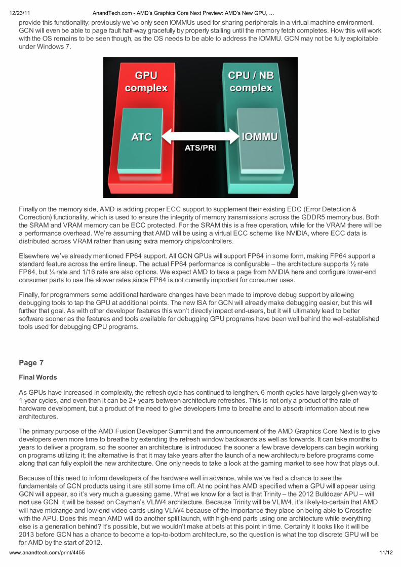
Now what’s interesting is that the unified address space that will be used is the x86-64 address space. All instructions sent toa GCN GPU will be relative to the x86-64 address space, at which point the GPU will be responsible for doing addresstranslation to local memory addresses. In fact GCN will even be incorporating an I/O Memory Mapping Unit (IOMMU) to
12/23/11 AnandTech.com - AMD's Graphics Core Next Preview: AMD's New GPU, …
11/12www.anandtech.com/print/4455
provide this functionality; previously we’ve only seen IOMMUs used for sharing peripherals in a virtual machine environment.GCN will even be able to page fault half-way gracefully by properly stalling until the memory fetch completes. How this will workwith the OS remains to be seen though, as the OS needs to be able to address the IOMMU. GCN may not be fully exploitableunder Windows 7.
Finally on the memory side, AMD is adding proper ECC support to supplement their existing EDC (Error Detection &Correction) functionality, which is used to ensure the integrity of memory transmissions across the GDDR5 memory bus. Boththe SRAM and VRAM memory can be ECC protected. For the SRAM this is a free operation, while for the VRAM there will bea performance overhead. We’re assuming that AMD will be using a virtual ECC scheme like NVIDIA, where ECC data isdistributed across VRAM rather than using extra memory chips/controllers.
Elsewhere we’ve already mentioned FP64 support. All GCN GPUs will support FP64 in some form, making FP64 support astandard feature across the entire lineup. The actual FP64 performance is configurable – the architecture supports ½ rateFP64, but ¼ rate and 1/16 rate are also options. We expect AMD to take a page from NVIDIA here and configure lower-endconsumer parts to use the slower rates since FP64 is not currently important for consumer uses.
Finally, for programmers some additional hardware changes have been made to improve debug support by allowingdebugging tools to tap the GPU at additional points. The new ISA for GCN will already make debugging easier, but this willfurther that goal. As with other developer features this won’t directly impact end-users, but it will ultimately lead to bettersoftware sooner as the features and tools available for debugging GPU programs have been well behind the well-establishedtools used for debugging CPU programs.
Page 7
Final Words
As GPUs have increased in complexity, the refresh cycle has continued to lengthen. 6 month cycles have largely given way to1 year cycles, and even then it can be 2+ years between architecture refreshes. This is not only a product of the rate ofhardware development, but a product of the need to give developers time to breathe and to absorb information about newarchitectures.
The primary purpose of the AMD Fusion Developer Summit and the announcement of the AMD Graphics Core Next is to givedevelopers even more time to breathe by extending the refresh window backwards as well as forwards. It can take months toyears to deliver a program, so the sooner an architecture is introduced the sooner a few brave developers can begin workingon programs utilizing it; the alternative is that it may take years after the launch of a new architecture before programs comealong that can fully exploit the new architecture. One only needs to take a look at the gaming market to see how that plays out.
Because of this need to inform developers of the hardware well in advance, while we’ve had a chance to see thefundamentals of GCN products using it are still some time off. At no point has AMD specified when a GPU will appear usingGCN will appear, so it’s very much a guessing game. What we know for a fact is that Trinity – the 2012 Bulldozer APU – willnot use GCN, it will be based on Cayman’s VLIW4 architecture. Because Trinity will be VLIW4, it’s likely-to-certain that AMD
will have midrange and low-end video cards using VLIW4 because of the importance they place on being able to Crossfirewith the APU. Does this mean AMD will do another split launch, with high-end parts using one architecture while everythingelse is a generation behind? It’s possible, but we wouldn’t make at bets at this point in time. Certainly it looks like it will be2013 before GCN has a chance to become a top-to-bottom architecture, so the question is what the top discrete GPU will befor AMD by the start of 2012.

12/23/11 AnandTech.com - AMD's Graphics Core Next Preview: AMD's New GPU, …
12/12www.anandtech.com/print/4455
Moving on, it’s interesting that GCN effectively affirms most of NVIDIA’s architectural changes with Fermi. GCN is all aboutcreating a GPU good for graphics and good for computing purposes; Unified addressing, C++ capabilities, ECC, etc were allfeatures NVIDIA introduced with Fermi more than a year ago to bring about their own compute architecture. I don’t believethere’s ever been a question whether NVIDIA was “right”, but the question has been whether it’s time to devote so muchengineering effort and die space on technologies that benefit compute as opposed to putting in more graphics units. WithNVIDIA and now AMD doing compute-optimized GPUs, clearly the time is quickly approaching if it’s not already here.
Larrabee As It Was: Scalar + 16-Wide Vector
I can’t help but to also make a comparison to Intel’s aborted Larrabee Prime architecture here. There are some veryinteresting similarities between Larrabee and GCN, primarily in the dual vector/scalar design and in the use of a 16-widevector ALU. Processing 16 elements at once is an incredibly common occurrence in GPUs – it even shows up in Fermi whichprocesses half a warp (16 threads) a clock. There are still a million differences between all of these architectures, but there’sdefinitely a degree of convergence occurring. Previously NVIDIA and AMD converged around VLIW in the days of thegraphical GPU, and now we’re converging at a new point for the compute GPU.
Finally, while we’ve talked about the GCN architecture in great detail we haven’t talked about how to program it. Of coursethere’s OpenCL, but with GCN there’s going to be so much more. Next week we will be taking a look at AMD’s FusionSystem Architecture, a high-level abstraction layer that will make GPU programming even more CPU-like, an advancementnecessary to bring forth the kind of heterogeneous computing AMD is shooting for. We will also be taking a look at Microsoft’sC++ Accelerated Massive Parallelism (AMP), a C++ extension to bridge the gap between current and future architectures byallowing developers to program for GPUs in C++ even if the GPU doesn’t fully support the C++ feature set.
It’s clear that 2011 is shaping up to be a big year for GPUs, and we’re not even half-way through. So stay tuned, there’s muchmore to come.