some basic issues and applications of switch-mode ...cdn.intechweb.org/pdfs/23867.pdfsome basic...
TRANSCRIPT
11
Some Basic Issues and Applications of Switch-Mode Rectifiers on Motor Drives
and Electric Vehicle Chargers
C. M. Liaw and Y. C. Chang National Tsing Hua University, National Chung Cheng University
Taiwan
1. Introduction
Switch-mode rectifier (SMR) or called power factor corrected (PFC) rectifier (Erickson & Maksimovic, 2001; Mohan et al, 2003; Dawande & Dubey, 1996) has been increasingly utilized to replace the conventional rectifiers as the front-end converter for many power equipments. Through proper control, the input line drawn current of a SMR can be controlled to have satisfactory power quality and provide adjustable and well-regulated DC output voltage. Hence, the operation performance of the followed power electronic equipment can be enhanced. Taking the permanent-magnet synchronous motor (PMSM) drive as an example, field-weakening and voltage boosting are two effective approaches to enhance its high-speed driving performance. The latter is more effective and can avoid the risk of magnet demagnetization. This task can naturally be preserved for a PMSM drive being equipped with SMR. Generally speaking, a SMR can be formed by inserting a suitable DC-DC converter cell between diode rectifier and output capacitive filter. During the past decades, there already have a lot of SMRs, the survey for single-phase SMRs can be referred to the related literatures. Since the AC input current is directly related to the pulse-width modulated (PWM) inductor current, the boost-type SMR possesses the best PFC control capability subject to having high DC output voltage limitation. In a standard multiplier based high-frequency controlled SMR, its PFC control performance is greatly affected by the sensed double-frequency voltage ripple. In (Wolfs & Thomas, 2007), the use of a capacitor reference model that produces a ripple free indication of the DC bus voltage allows the trade off regulatory response time and line current wave shape to be avoided. A simple robust ripple compensation controller is developed in (Chen et al, 2004), such that the effect of double frequency ripple contaminated in the output voltage feedback signal can be cancelled as far as possible. In (Li & Liaw, 2003), the quantitative digital voltage regulation control for a zero-voltage transition (ZVT) soft-switching boost SMR was presented. As to (Li & Liaw, 2004b), the robust varying-band hysteresis current-controlled (HCC) PWM schemes with fixed and varying switching frequencies for SMR have been presented. In (Chai & Liaw, 2007), the robust control of boost SMR considering nonlinear behavior was presented. The adaptation of voltage robust compensation control is made according to the observed nonlinear phenomena. The development and control for a SRM drive with front-end boost SMR were presented in (Chai & Liaw, 2009). In (Chai et al, 2008), the novel random
www.intechopen.com

Electrical Generation and Distribution Systems and Power Quality Disturbances
252
switching approach was developed for effectively reducing the acoustic noise of a low-frequency switching employed in a PMSM drive. In the bridgeless SMRs developed in (Huber et al, 2008), the higher efficiency is achieved by reducing loop diode voltage drops. In some occasions, the galvanic isolation of power equipment from AC source is required. In (Hsieh, 2010), a single-phase isolated current-fed push pull (CFPP) boost SMR is developed, and the comparative evaluation for the PMSM drive equipped with standard, bridgeless and CFPP isolated boost SMRs is made. From input-output voltage magnitude relationship, the buck-boost SMR is perfect in performing power factor correction control (Erickson & Maksimovic, 2001; Matsui et al, 2002). And it is free from inrush current problem owing to its indirect energy transfer feature. However, the traditional non-isolated buck-boost SMR possesses some limitations: (i) without isolation; (ii) having reverse output voltage polarity; (iii) discontinuous input and output currents; and (iv) having relatively high voltage and current stresses due to zero direct power transfer. As generally recognized, the use of high-frequency transformer isolated buck-boost SMR can avoid some of these limitations. The performance comparison study among Cuk, single ended primary inductor converter (SEPIC), ZETA and flyback SMRs in (Singh et al, 2006) concludes that the flyback SMR is the best one in the control performance and the required number of constituted component. In (Lamar et al, 2007), in addition to the power rating limits, the limitations of flyback SMR in PFC characteristics and output voltage dynamic response are discussed. In (Papanikolaou et al, 2005), the design of flyback converter in CCM for low voltage application is presented. In the power circuit developed in (Lu et al, 2003), a dual output flyback converter is employed to reduce the storage capacitor voltage fluctuation against input voltage and load changes of flyback SMR in DCM. Similarly, two flyback converters are also used in the flyback SMRs developed in (Zheng & Moschopoulos, 2006) and (Mishra et al, 2004) to achieve direct power transfer and improved voltage regulation control characteristics. As to the single-stage SMR developed in (Lu et al, 2008), it combines a boost SMR front-end and a two-switch clamped flyback converter. Similarly, an intermediate energy storage circuit is also employed. In (Rikos & Tatakis, 2005), a new flyback SMR with non-dissipative clamping is presented to obtain high power factor and efficiency in DCM. The proposed clamping circuit utilizes the transformer leakage inductance to improve input current waveform. In (Jang et al, 2006), an integrated boost-flyback PFC converter is developed. The soft switching of all its constituted switches is preserved to yield high efficiency. On the other hand, the improved efficiency of the flyback converter presented in (Lee et al, 2008) is obtained via the use of synchronous rectifier. It is known that digital control for power converter is a trend to promote its miniaturization. In (Newsom et al, 2002), the control scheme realization is made using off-the-shelf digital logic components. And recently, the VLSI design of system on chip application specific integrated circuit (SoC-ASIC) controller for a double stage SMR has also been studied in (Langeslag et al, 2007). It consists of a boost SMR and a flyback DC-DC converter. The latter is controlled using valley-switching approach operating in quasi-resonant DCM, which has fixed on-time and varying off-time according to load. As far as the switching control strategies are concerned, they can be broadly categorized into voltage-follower control (Erickson & Madigan, 1990) and current-mode control (Backman & Wolpert, 2000). The former belongs to open-loop operation under DCM, and thus the current feedback control is not needed. As to the latter, the multiplier-based current control loop is necessary to achieve PFC control. Basically, the commonly used PWM switching control approaches for a flyback SMR include peak current control (Backman & Wolpert,
www.intechopen.com

Some Basic Issues and Applications of Switch-Mode Rectifiers on Motor Drives and Electric Vehicle Chargers
253
2000), average current control, charge control and its modifications (Tang et al, 1993). In the peak current controlled flyback converter presented in (Backman & Wolpert, 2000), the proper choice of magnetizing inductance is suggested to reduce the distortion of input current. In (Tang et al, 1993; Larouci et al, 2002), after turning on the switch at clock, the switch is turned off as the integration of switch current is equal to the control voltage. As to (Buso et al, 2000), a modified nonlinear carrier control approach is developed to avoid the sense of AC input voltage. For easily treating the dynamic control of a single-stage PFC converter, its general dynamic modeling and controller design approaches have been conducted in (Uan-Zo-li et al, 2005). In addition, there were also some special control methods for flyback SMR. See for example, a simplified current control scheme using sensed inductor voltage is developed in (Tanitteerapan & Mori, 2001). In (Y.C. Chang & Liaw, 2009a), a flyback SMR in DCM with a charge-regulated PWM scheme is developed. For a SMR, the nonlinear behavior and the double-frequency voltage ripple may let the closed-loop controlled SMR encounter undesired nonlinear phenomena (Orabi & Ninomiya, 2003). The key parameters to be observed in nonlinear behavior of a SMR will be the loading condition, the value of output filtering capacitor and the voltage feedback controller parameters. In the flyback SMR developed in (Y.C. Chang & Liaw, 2009a), the simple robust control is proposed to avoid the occurrence of nonlinear phenomena, and also to improve the SMR operating performance. Random PWM switching is an effective means to let the harmonic spectrum of a power converter be uniformly distributed. Some typical existing studies concerning this topic include the ones for motor drives (Liaw et al, 2000), DC-DC converters (Tse et al, 2000), SMRs (Li & Liaw, 2004b; Chai et al, 2008), etc. In the flyback SMR developed by (Y.C. Chang & Liaw, 2011), to let the harmonic spectrum be dispersdly distributed, a random switching scheme with fixed turn-on period and varying turn-off period is presented. Although flyback SMR possesses many merits, it suffers from the major limitation of having limited power rating. To enlarge the rating, the parallel of whole isolated converter of flyback SMR was made in (Sangsun & Enjeti, 2002). In the existing interleaved flyback converters, the researches made in (Forest et al, 2007, 2009) are emphasized on the use of intercell transformers. However, the typical interleaving of flyback SMR requires multiple switches and diodes, which increases the cost and complexity of power circuit. For a single-phase flyback SMR, the major DC output voltage ripple is double line frequency component. Hence PWM interleaving control is not beneficial in its ripple reduction. Moreover, the power limitation of flyback transformer is more critical than the other system active components. It follows that sole parallel of transformer (Manh & Guldner, 2006; Inoue et al, 2008) will be the convenient way to enlarge the rating of whole flyback SMR. In (Y.C. Chang & Liaw, 2009b), the rating enlargement is made by parallel connection of transformer. For the power equipments with higher ratings, the three-phase SMR is a natural choice for higher rated plants. The systematic surveys for the existing three-phase SMRs can be found in (Hengchun et al, 1997; Shah et al, 2005). Similar to transformers, three-phase SMRs can also be formed using multiple single-phase SMR modules via proper connection (Hahn et al, 2002; Li & Liaw, 2004c). For simplicity and less stringent performance, the three-phase single-switch (3P1SW) SMR will be a good choice. In the 3P1SW SMR presented in (Chai et al, 2010), a robust current harmonic cancellation scheme and a robust voltage control scheme are developed. The undesired line current and output voltage ripples are regarded as disturbances and they are reduced via robust controls. In voltage control, a feedback controller is augmented with a simple robust error canceller. The robust cancellation
www.intechopen.com
Electrical Generation and Distribution Systems and Power Quality Disturbances
254
weighting factor is automatically tuned according to load level to yield compromised voltage and power quality control performances. Similar to single-phase bridgeless SMRs (Zhang et al, 2000; Youssef et al, 2008), there were also some researches being emphasized on the development of three phase bridgeless SMRs (Reis et al, 2008; Oliverira et al, 2009). In (Wang, 2010), a bridgeless DCM three phase SMR is developed and used as a front-end AC-DC converter for the SRM drive. As generally recognized, soft-switching can be applied for various converters to reduce their switching lossess, voltage stresses and electromagnetic interference. The applications of soft-switching in 3P1SW SMRs have also been conducted in (Gataric et al, 1994; Ueda et al, 2002). For the 3P1SW SMR operating under DCM, only the zero-current switching (ZCS) at turn-off is effective in reducing its switching losses. In (Wang, 2010), the zero-current transition (ZCT) (Gataric et al, 1994) is utilized to the developed 3P1SW to achieve the ZCS of the main switch at turn-off. In realization, an auxiliary resonant branch is added, and the proper switching signals are generated for the main and auxiliary switches. The soft-switching can be achieved without adding extra sensors. And also in (Wang, 2010), the comparative performance evaluation is made for the SRM drive powered using standard 3P1SW SMR, ZCT 3P1SW SMR and bridgeless DCM three phase SMR.
2. Power factor correction approaches
For facilitating the research made concerning power quality, the commonly referred harmonic standard is first introduced. Then the possible power factor correction approaches are described to comprehend their comparative features.
2.1 Harmonic ccurrent emission standard IEC 61000-3-2 (previously, IEC-555) is the worldwide applied harmonic current emission standard. This standard specifically limits harmonics for equipments with an input current up to 16A, connected to 50Hz or 60Hz, 220V to 240V single phase circuit (two or three wires). The IEC 61000-3-2 standard distinguishes the loads into four classes with different harmonic limits (Erickson & Maksimovic, 2001; Mohan et al, 2003). From the contents one can find that for the equipments below 600W, the harmonic limits of Class A are larger than those of Class D. This advantage will be more significant for lower power level. Taking the third harmonic under 100W as an example, the limit in Class A is 2.3A compared to 0.34A in Class D. Power converter can apply Class D or Class A regulation depending on its input current wave shape. The peaky line drawn current of a diode rectifier with larger filtering capacitor definitely belongs to Class D. However, if the simple low-frequency switching SMR (Chai et al, 2008) is employed, the modified line drawn current may fall into Class A and thus possesses the advantage mentioned above.
2.2 Possible power factor correction methods Depending on rating, schematic and control complexities, control performance and cost, there are many possible power factor correction approaches. The suited and cost effective one can be chosen according to the desired performance for specific application.
2.2.1 Passive filter Various series L-C resonant trap filters are connected across the line terminal to attenuate the specific order harmonics. This approach is simple, rugged, reliable and helpful in
www.intechopen.com

Some Basic Issues and Applications of Switch-Mode Rectifiers on Motor Drives and Electric Vehicle Chargers
255
reducing EMI. However, it is bulky and cannot completely regulate nonlinear loads, and it is needed the redesign adapted to load changes.
2.2.2 Active power filter Compared with passive filter, active power filter (APF) has the higher control ability to compensate load reactive and harmonic current components. According to the types of connections, active power filters can be categorized into series, shunt and hybrid types (Erickson & Maksimovic, 2001; Mohan et al, 2003). Taking the shunt type active power filter as an example, a controlled current is generated from the APF to compensate the load ripple current as far as possible.
2.2.3 Passive PFC circuits Fig. 1(a) shows the sketched key waveforms of a full-bridge rectifier with large and small filtering capacitors. One can be aware that if a very small filtering capacitor is employed, the line drawn power quality is improved, and thus the Class A rather than the Class D is applied. However, the effects of DC-link voltage ripple should be considered in making the control of the followed power stage. Recently, to reduce the rectified DC voltage ripple, some plants employ the valley-fill filter as shown in Fig. 1(b) (Farcas et al, 2006).
t
tcθ
acv
aci
dcv
acvaci dcv
acv
aci
t
acv
acidcv
acv
aci
dcv
(h)
Load
dcv
Load
(a)
dcC
dcC Small
dcC Large
filter fillValley −
Fig. 1. Some passive PFC circuits: (a) rectifier with small filtering capacitor; (b) rectifier using valley-fill filter
www.intechopen.com

Electrical Generation and Distribution Systems and Power Quality Disturbances
256
2.2.4 Switch-mode rectifier
The SMRs possess many categories in circuit topology and switching control approaches. A
single-phase boost-type SMR is shown in Fig. 2(a), and the typical waveforms of aci using
low-frequency (LF) and high-frequency (HF) switchings are sketched in Figs. 2(b) and 2(c).
The features of HF-SMR comparing to LF-SMR are: (i) more complicated in control; (ii) high
control performances in line drawn current, power factor and output voltage; (iii) lower
efficiency. More detailed survey for SMRs will be presented in the latter paragraphs.
acv
L Daci
S
tω tω
dcv
Load
dcCiv
Li Di
aci *aci acv
aci
acv
dθ onθ
(a)
(b)(c)
Fig. 2. Boost-type SMR: (a) circuit; (b) sketched key waveforms for low-frequency switching; (c) sketched waveforms for high-frequency switching
3. Classification of SMRs
Basically, a SMR is formed by inserting a suited DC/DC converter between diode rectifier and capacitive output filter, under well regulated DC output voltage, the desired AC input line drawn power quality can be achieved. The existing SMRs can be categorized as:
1. Schematics
a. Single-phase or three-phase: each category still possesses a lot of types of SMR schematics. The three-phase SMR will be a natural choice for larger power plants.
b. Non-isolated or isolated: although the former SMR is simpler and more compact, the latter one should be used if the galvanic isolation from mains is required. See for example, the flyback SMR is gradually employed in communication distributed power architecture as a single-stage SMR front-end, or called silver box, to establish -48V DC-bus voltage.
c. Voltage buck, boost or buck/boost: depending on the input-output relative voltage levels, suited type of SMR and its control scheme should be chosen. Basically, the boost-type SMR possesses the best current control ability subject to having high DC output voltage level.
d. Single-stage or multi-stage: generally speaking, the stage number should be kept as small as possible for achieving higher efficiency and system compactness. Hence, single-stage SMR is preferable if possible.
www.intechopen.com

Some Basic Issues and Applications of Switch-Mode Rectifiers on Motor Drives and Electric Vehicle Chargers
257
e. One-quadrant or multi-quadrant: multiple quadrant SMR may possess reverse power flow from DC side to AC source, such as the regenerative braking of a SMR-fed AC motor drive can be performed by sending braking energy back to the utility grid.
f. Hard-switching or soft-switching: Similarly, suited soft switching technique can also be applied to reduce the switching loss, switching stress and EMI of a SMR (Li & Liaw, 2003; Wang, 2010).
2. Control methods
a. Low-frequency control: only v-loop is needed and only one switching per half AC cycle is applied. It is simple but has limited power quality characteristics.
b. High-frequency control- voltage-follower control: without current control loop, only some specific SMRs operating in DCM possess this feature, see for example, buck-boost SMR and flyback SMR.
c. High-frequency control- standard control: it belongs to multiplier-based current-mode control approach with both v- and i- control loops.
3.1 Single-phase SMRs The typical existing single-phase SMR circuits include: (a) boost SMR; (b) buck SMR; (c) buck- boost SMR; (d) Ćuk SMR; (e) SEPIC SMR with coupled inductors; (f) SEPIC SMR; (g) ZETA SMR; (h) buck-boost cascade SMR; (i) boost-buck hybrid SMR; (j) flyback SMR; (k) isolated Ćuk SMR; and (l) isolated ZETA SMR. Some comments are given for these circuits: (i) The SMRs of (a) to (i) belong to non-isolated types, whereas (j) to (l) are isolated ones; (ii) Among the non-isolated SMRs, the boost-type SMR possesses the best PFC control performance, since its AC input current is directly related to the switched inductor current; (iii) The circuits of (d), (i) and (k) possess the common features of having both continuous input and output currents, and hence needing less stringent filter design requirement. In addition to the SMRs of (j) to (l) mentioned above, some isolated SMRs specifically for PMSM drives (Singh B. & Singh S., 2010) include: (a) push-pull buck; (b) push-pull boost; (c) half-bridge buck; (d) half-bridge boost; (e) full-bridge buck; (f) full-bridge boost. The push-pull boost SMR possesses excellent PFC control ability and high voltage boost ratio.
3.2 Three-phase SMRs Detailed surveys for the existing three-phase SMR circuits can be referred to (Hengchun et al, 1997; Shah & Moschopoulos, 2005). The complexities of schematic and control mechanism depend on the control ability and the desired performances. Some commonly used boost-type SMRs are briefly introduced as followed.
3.2.1 Three-leg six-switch standard SMR The standard three-phase six-switch SMR (Hengchun et al, 1997; Shah & Moschopoulos, 2005) possesses four operation quadrants and high flexibility in power conditioning control. For a motor drive equipped with such SMR, it may possess regenerative braking ability. However, the switch utilization ratio of this SMR is low, and its control is complicated.
3.2.2 Four-leg eight-switch SMR In the four-leg three-phase SMR (Zhang et al, 2000) with eight switches, the additional fourth leg can be arranged to regulate the imbalance caused by source voltage and switching operation, and it can provide fault tolerant operation.
www.intechopen.com
Electrical Generation and Distribution Systems and Power Quality Disturbances
258
3.2.3 Three-switch Vienna SMR
The Vienna three-phase SMR (Youssef et al, 2008) uses only three switches to achieve good
current command tracking control. It can be regarded as a simplified version of three single-
phase PFCs connected to the same intermediate bus voltage. The major features of this SMR
are: (i) three output voltage levels ( 0.5 ov , ov , -0.5 ov ) providing larger switching control
flexibility; (ii) lower switch voltage rating, 0.5 ov rather than ov ; and (iii) lower input current
distortion. However, it has only unidirectional power flow capability, and needs
complicated power switch and two serially connected capacitors. The specific power switch
(VUM 25-05) for implementing this SMR is avaiable from IXYS Corporation, USA.
3.2.4 Single-switch SMR
The three-phase single-switch SMR (3P1SW) possesses the simplest schematic and control
scheme. By operating it in DCM, the PFC is naturally preserved without applying current
PWM control. However, it possesses the limits: (i) Having higher input peak current and
switch stress; (ii) The input line current contains significant lower-frequency harmonics with
the orders of 6n ± 1, n=1, 2, …, and the dominant ones are the 5th and 7th harmonics. Thus
suitably designed AC-side low-pass filter is required to yield satisfactory power quality; (iii)
The line drawn power quality is limited, typically the power factor is slightly higher than
0.95; (iv) Similarly, this 3P1SW SMR possesses only one-quadrant capability. To improve the input power quality of this three-phase single-switch SMR, many existing researches have been conducted, see for example: (i) Fifth-order harmonic band-stop filtering; (ii) Harmonic-injection approach; (iii) Variable switching frequency controls; (iv) Passive filtering and input current steering; (v) Optimum PWM pattern; and (vi) Injected PWM robust compensation control. In (Chai et al, 2010), the robust current harmonic cancellation scheme is developed to yield improved line drawn power quality. The robust cancellation weighting factor is automatically tuned according to load level.
3.2.5 Two-switch SMR This SMR (Badin & Barbi, 2008) is constructed by two serially connected DC/DC boost converter cells behind the rectifier. It possesses only unidirectional power flow capability. The boost converters are applied to shape the input currents, and the current injection device is used to inject the third-harmonic currents in front of the diode bridge to improve the line drawn power quality. This converter uses fewer switches but possesses higher input current harmonics.
3.2.6 Modular connection using single-phase SMRs Similar to three-phase transformers, three-phase SMRs can also be formed by suitable connection of multiple single-phase modules (Hahn et al, 2002; Li & Liaw, 2004c). Fig. 3(a)
shows a Y-connected three-phase boost-type SMR. For Δ − connected three-phase SMR, when one module is faulted, the remaining two modules can continuously provide DC power output subject to the reduction of rating.
3.2.7 Bridgeless SMR As shown in Fig. 3(b) (Reis et al, 2008; Oliverira et al, 2009), the SMR uses three diodes and three switches rather than using diode bridge rectifier. Obviously, one diode drop is
www.intechopen.com

Some Basic Issues and Applications of Switch-Mode Rectifiers on Motor Drives and Electric Vehicle Chargers
259
eliminated in each line-current path resulting to increase the efficiency compared to single-switch SMR. However, two additional power switches are employed.
SW
1
Control circuit
n
Load
(a)
Single-phase boost SMR power stage
LZ
vK
Control circuit
Control circuit
SW
anv
cnv
bnv
dC ov
oi
SW
SW
1bL
2bL 2D
1D
φ SMR
1φ SMR
1φ SMR
fL
fL
fL
fC
fC
fC
1bL
2bL
3bL
1bi
2bi
3bi
dC
anv
bnv
cnv
n
ani
bni
cni
abv
LZ
(b)
dv Load
Fig. 3. Two types of SMRs: (a) modular connection of three single-phase SMRs; (b) bridgeless DCM three-phase SMR
3.3 Three-phase single-switch ZCT SMRs The soft-switching SMRs using auxiliary switching circuit can be generally classified into zero-voltage-transition (ZVT) and zero-current-transition (ZCT). The choice depends on the semiconductor devices to be used. The ZVS approaches are generally recommended for MOSFET. On the other hand, ZCS approaches are effective for IGBT. Some existing soft-switching SMRs are introduced as follows:
3.3.1 Classical three-phase single-switch ZCT SMR The classical 3P1SW ZCT SMR (Wang et al, 1994) is simple in structure and easy to realize. However, the auxiliary switch is not operated on ZCS at turn-off. The efficiency is limited.
3.3.2 Modified three-phase single-switch ZCT SMR In the modified 3P1SW ZCT SMR presented in (Das & Moschopoulos, 2007). The addition of the transformer in the auxiliary circuit let the circulating energy from the auxiliary circuit be transferred to the output. Hence it possesses higher efficiency than the classical type.
3.3.3 Three-phase three-switch bridgeless ZCT SMR As to the three-phase bridgeless ZCT SMR (Mahdavi & Farzanehfard, 2009), the auxiliary circuit provides soft-switching condition through ZCT approach for all semiconductor devices without any extra current and voltage stress.
www.intechopen.com

Electrical Generation and Distribution Systems and Power Quality Disturbances
260
4. Operation principle and some key issues of SMR
4.1 Single-phase SMRs
Fig. 4 shows the conceptual configuration of a single-phase SMR. The AC source input
voltage is expressed as sin 2 sinac m acv V t V tω ω= = . If the AC input current aci can be
regulated to be sinusoidal and kept in phase with acv , then the ideal SMR is similar to an
emulated resistor with the effective resistance of eR viewing from the utility grid. In reality,
the double line frequency output voltage ripple always exists for an actual SMR with finite
value of output filtering capacitor. This ripple may contaminate to distort the current
command, and hence to worsen the power quality control performance. The output power
( )p t of the SMR shown in Fig. 4 can be expressed as:
2 2 2 22
2 2
2
( ) sin (1 cos2 ) cos22
cos2
m m ac acac
e e e e
d acd ac
d e
V V V Vp t P t t t
R R R R
V Vt P P
R R
ω ω ω
ω
= = = − = −
= − Δ +
(1)
where dP and 2acP respectively denote the output DC and the double-frequency power
components. From the average power invariant property in (1), one can obtain the following
equivalent resistance transfer relationship:
DC/DC converter cell
dv
+
−
SiLi Di
acv
aci
+
−
+
− cr
Control scheme
acv
dv
( )p t
dC
di
eR )(td
od PP =dac PP =
aci vv =
aci ii =
Li
Di
dR
Fig. 4. Conceptual configuration of a single-phase SMR
d d
ac e
V R
V R= (2)
By neglecting the capacitor ESR cr in Fig. 4, the current ( )di t can be found from (1):
2
2
( )( ) (1 cos2 )ac
d d d
d e d
p t Vi t t I i
V R Vω≅ = − = + (3)
The AC component 2di is approximately regarded flowing through the capacitor:
2( )
cos2d acd
e d
d v t VC t
dt R Vω
Δ= − (4)
www.intechopen.com

Some Basic Issues and Applications of Switch-Mode Rectifiers on Motor Drives and Electric Vehicle Chargers
261
Then the voltage ripple ( )dv tΔ can be found by integrating the above equation:
2 21 1
( ) cos2 sin22
ac acd
d e d d d e
V Vv t tdt t
C R V C V Rω ω
ωΔ = − = 1
sin22
d
d d
Vt
C Rω
ω= (5)
From (5) one can get the peak to peak value of output ripple voltage:
dd
d d
Vv
C RωΔ = (6)
4.2 Three-phase SMRs 4.2.1 Three-Phase Single-Switch (3P1SW) SMR
For a well-regulated three-phase single-switch (3P1SW) DCM SMR shown in Fig. 5, it can be
regarded as a loss-free emulated resistor eR viewing from the phase AC source with line
drawn current having dominant 5th and 7th harmonics (Chai et al, 2010). Hence, the three-
phase line drawn instantaneous power can be approximately expressed as:
2
2
2
2
sin 1 1[sin sin 5 sin7 ]
5 7
sin( 2 / 3) 1 1 [sin( 2 / 3) sin 5( 2 / 3) sin7( 2 / 3)]
5 7
sin( 2 / 3) 1 1 [sin( 2 / 3) sin 5( 2 / 3) sin7( 2 / 3)]
5 7
3
2
mac an a bn b cn c
e
m
e
m
e
m
V tp v i v i v i t t t
R
V tt t t
R
V tt t t
R
V
ωω ω ω
ω πω π ω π ω π
ω πω π ω π ω π
= + + = − − +
−− − − − − +
++ − + − +
=23
cos635
mac ac
e e
Vt P p
R Rω δ− Δ +
(7)
where acP = average AC power, acpδ = ripple AC power. By neglecting all power losses, one
has o dP P= , i.e.,
2 23
2m d
ac
e d
V VP
R R= = (8)
DS
anv
a bv
cnv
n
fL
fL
fL
fC
fC
fC
bLai
bi
ci
1bi
2bi
3bi
bnv bL
bL
+
−
dCdRdv
LoadDi
+
+
a
b
c
+
+ eRod PP =dac PP =
Control schemedv
)(td
Fig. 5. Conceptual configuration of a three-phase DCM SMR
www.intechopen.com
Electrical Generation and Distribution Systems and Power Quality Disturbances
262
Then from (7) and (8), the AC charging current flowing the output filtering capacitor is:
2
cos635
d dd
d
dv VC t
dt Rω= − (9)
Thus one can derive the peak-to-peak output voltage ripple:
2
105d
d
d d
Vv
R CωΔ = (10)
4.2.2 Three-phase three-switch and six-switch SMRs For the Vienna SMR and three-phase six-switch standard SMR with ideal current mode control, the three-phase line drawn currents will be balanced without harmonics. Hence, from (7) one can find that the DC output voltage ripple will be nearly zero.
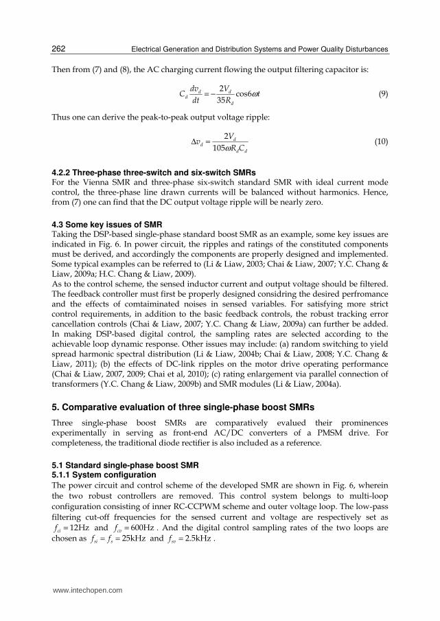
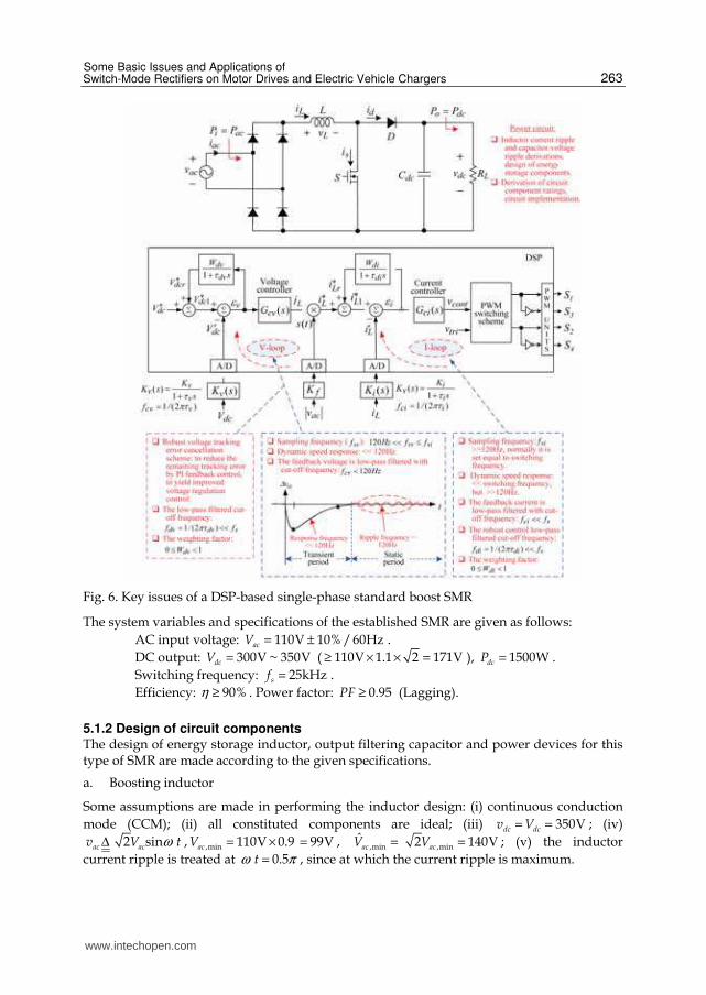
4.3 Some key issues of SMR Taking the DSP-based single-phase standard boost SMR as an example, some key issues are indicated in Fig. 6. In power circuit, the ripples and ratings of the constituted components must be derived, and accordingly the components are properly designed and implemented. Some typical examples can be referred to (Li & Liaw, 2003; Chai & Liaw, 2007; Y.C. Chang & Liaw, 2009a; H.C. Chang & Liaw, 2009). As to the control scheme, the sensed inductor current and output voltage should be filtered. The feedback controller must first be properly designed considring the desired perfromance and the effects of comtaiminated noises in sensed variables. For satisfying more strict control requirements, in addition to the basic feedback controls, the robust tracking error cancellation controls (Chai & Liaw, 2007; Y.C. Chang & Liaw, 2009a) can further be added. In making DSP-based digital control, the sampling rates are selected according to the achievable loop dynamic response. Other issues may include: (a) random switching to yield spread harmonic spectral distribution (Li & Liaw, 2004b; Chai & Liaw, 2008; Y.C. Chang & Liaw, 2011); (b) the effects of DC-link ripples on the motor drive operating performance (Chai & Liaw, 2007, 2009; Chai et al, 2010); (c) rating enlargement via parallel connection of transformers (Y.C. Chang & Liaw, 2009b) and SMR modules (Li & Liaw, 2004a).
5. Comparative evaluation of three single-phase boost SMRs
Three single-phase boost SMRs are comparatively evalued their prominences experimentally in serving as front-end AC/DC converters of a PMSM drive. For completeness, the traditional diode rectifier is also included as a reference.
5.1 Standard single-phase boost SMR 5.1.1 System configuration
The power circuit and control scheme of the developed SMR are shown in Fig. 6, wherein
the two robust controllers are removed. This control system belongs to multi-loop
configuration consisting of inner RC-CCPWM scheme and outer voltage loop. The low-pass
filtering cut-off frequencies for the sensed current and voltage are respectively set as
12Hzcif = and 600Hzcvf = . And the digital control sampling rates of the two loops are
chosen as 25kHzsi sf f= = and 2.5kHzsvf = .
www.intechopen.com
Some Basic Issues and Applications of Switch-Mode Rectifiers on Motor Drives and Electric Vehicle Chargers
263
Fig. 6. Key issues of a DSP-based single-phase standard boost SMR
The system variables and specifications of the established SMR are given as follows:
AC input voltage: 110V 10% /60HzacV = ± .
DC output: 300V ~ 350VdcV = ( 110V 1.1 2 171V≥ × × = ), 1500WdcP = .
Switching frequency: 25kHzsf = .
Efficiency: 90%η ≥ . Power factor: 0.95PF ≥ (Lagging).
5.1.2 Design of circuit components The design of energy storage inductor, output filtering capacitor and power devices for this type of SMR are made according to the given specifications.
a. Boosting inductor
Some assumptions are made in performing the inductor design: (i) continuous conduction
mode (CCM); (ii) all constituted components are ideal; (iii) 350Vdc dcv V= = ; (iv)
2 sin ac acv V tωΔ , ,min 110V 0.9acV = × 99V= , ,min ,minˆ 2 140Vac acV V= = ; (v) the inductor
current ripple is treated at 0.5tω π= , since at which the current ripple is maximum.
www.intechopen.com

Electrical Generation and Distribution Systems and Power Quality Disturbances
264
The maximum inductor current occurred at 0.5tω π= can be calculated as
max
,min
1500ˆ( ) 2 2 23.81Aˆ 110 2 0.9 0.9
dcL
ac
Pi
V η= × = × =
× × × (11)
Let the inductor current ripple be:
,minmax
ˆˆ0.1( ) 2.38Aac s
L L
V DTi i
LΔ = ≤ = (12)
The instantaneous duty ratio at 0.5tω π= can be found as:
,minˆ 350 140
0.6350
dc ac
dc
V VD
V
− −= = = (13)
Hence from (12) and (13), the condition of boosting inductance L is obtained as:
,minˆ
1.41mHac
s L
V DL
f i≥ =
Δ (14)
The inductor L is formed by serially connected two available inductors 1L and 2L . The
measured inductances using HIOKI 3532-50 LCR meter are 1L = (2.03mH, ESR = 210mΩ at
60Hz, and 1.978mH, ESR= 5.68Ω at 25kHz) and 2L = (2.11mH, ESR= 196mΩ at 60Hz, and
1.92mH, ESR= 62Ω at 25kHz). Hence 1 2L L L= + =4.14mH, which is suited here.
b. Output capacitor
By choosing the output filtering capacitor 2200 F/450VdC µ= , the peak-to-peak output
voltage ripple can be found as:
6
1 1
15005.17V
2 60 2200 10 350dc dc
dc
L d d dc
V PV
R C C Vω ω π −Δ = = = =
× × × × (15)
c. Power semiconductor devices
The maximum current of the main switch S and the diode D is maxˆ( ) 0.5 25AL Li i+ Δ = , which
is calculated from (11) and (12), and their maximum voltage is 350V. Accordingly, the
MOSFET IXFK44N80P (IXYS) (800V, ID= 44A (continuous), IDM = 100A (pulsed)) and the
fast diode DSEP60-06A (IXYS) (600V, average current IFAVM = 60A) are chosen for
implementing the main switch S and all diodes respectively.
5.1.3 Control schemes Current controller:
he current feedback controller ( )ciG s in Fig. 6 is chosen to be PI-type:
( ) Iici Pi
KG s K
s= + (16)
The upper limit of the P-gain is first determined based on large-signal stability at switching frequency:
www.intechopen.com

Some Basic Issues and Applications of Switch-Mode Rectifiers on Motor Drives and Electric Vehicle Chargers
265
dc accont tri
Pi i
V vdv dvK K
dt L dt
−= < (17)
The parameters of the developed SMR shown in Fig. 6 are set as: 300VdcV = , 0.04V/AiK = ,
25kHzsf = , L = 4.14mH and 25kV/sectridv dt = . Using the given data, the upper value of
the PiK can be found from (17) to be 8.625Pi PiK K< = ( 0acv = is set here). Accordingly
4.0PiK = is set.
In making the determination of integral gain, the magnitude frequency response of the loop
gain '( ) ( ) / ( )L i s jLG s j i s s ωω ε == Δ is measured using the HP 3563A control systems analyzer
as shown in Fig. 7, wherein injV denotes an injected swept sine signal. Fig. 8 shows the
measured magnitude frequency response of the loop gain. The measurement conditions are
set as: (i) , 10mVinj peakv = ; (ii) swept sine frequency range is from 400Hz to 11kHz; (iii) the
voltage loop is opened, and the current command is set as * ˆL L acI I v= × with ˆ 8ALI = ; (iv)
200LR = Ω ; (v) rms110Vacv = ; (vi) the current feedback controllers are set as 4PiK = and
45000IiK = . The measured result in Fig. 8 indicates that the crossover frequency is
1.47kHz / 2c sf f= < , which is reasonable for a ramp-comparison current-controlled PWM
scheme. Hence finally,
45000
( ) 4Iici Pi
KG s K
s s= + = + (18)
If the measurement of loop-gain frequency response is not convenient, one can also use the derived small-signal dynamic model (Chai & Liaw, 2007), or using trail-and-error approach to determine the integral gain.
Fig. 7. System configuration in current loop gain measurement
20.0
-20.0400Hz 11kHz
0
1.47kHz
1kHz
Mag
nit
ud
e (d
B)
Frequency (Hz)
Fig. 8. Measured magnitude frequency response of current loop gain
www.intechopen.com

Electrical Generation and Distribution Systems and Power Quality Disturbances
266
Voltage controller: Although the quantitative controller design can be achieved (Y.C. Chang & Liaw, 2009a), the PI voltage feedback controller is chosen trial-and-error here to be:
200
( ) 8Ivcv Pv
KG s K
s s= + = + (19)
5.1.4 Experimental results
Let acV =110 V /60Hz and 300VdcV = , the measured efficiencies η , iTHD of aci and PF at
( 400ΩLR = , dcP =227.7W ) and ( 200ΩLR = , dcP =473.6W ) are summarized in Table 1. And
the measured ( *Li , Li′ ) and ( acv , aci ) under ( 200ΩLR = , dcP =473.6W ) are shown in Figs. 9(a)
and 9(b). The results indicate that the input current aci is nearly sinusoidal and kept almost
in phase with the utility voltage acv . Good line drawn power quality can also be observed
from Table 1.
Load casesVariables
Resistive load
( 400ΩLR = )
Resistive load
( 200ΩLR = )
acV 110V/60Hz 110V/60Hz
acP 241.6W 502.2W
dcV 300.8V 300.2V
dcP 227.7W 473.6W
η 94.25% 94.31%
iTHD 6.61% 6.11%
PF (Lagging) 0.992 0.994
Table 1. Measured steady-state characteristics of the standard boost SMR under two loads
100V
20Aaci
acv
5ms
6.25A
1ms
Li′*
Li
(a)
(b)
Fig. 9. Measured results of the standard boost SMR at 200ΩLR = : (a) ( *Li , Li′ ); (b) ( acv , aci )
www.intechopen.com

Some Basic Issues and Applications of Switch-Mode Rectifiers on Motor Drives and Electric Vehicle Chargers
267
5.2 Bridgeless boost SMR 5.2.1 System configuration Fig. 10 shows the bridgeless boost SMR, its control scheme is identical to those shown in Fig. 6 with the two switches being respectively operated in positive and negative half cycles. Although the efficiency of bridgeless SMR can be slightly increased, it possesses the common mode EMI problem due to the large parasitic capacitance between the output and ground, which provides a relatively low impedance path. To reduce this problem, the boosting inductor is divided into two equal inductors, and they are placed at AC source side.
5.2.2 Circuit design
The specifications are identical to those listed above. The two inductors 1L and 2L in Sec.
5.1.2 are used here as the two bridgeless boost SMR inductors, i.e., 1 2 0.5L L L= = .
dcVdcCLR
dcP
aci
acv
Li0.5L
0.5L
1S 2S
acP
Fig. 10. Schematic and control scheme of the developed bridgeless boost SMR
5.2.3 Control schemes
Current controller: Following the similar process introduced in Sec. 5.1.3 one can get
8.625Pi PiK K< = . Hence, 3.0PiK = is set and the integral gain is chosen via trial-and-error.
Finally:
2000
( ) 3Iici Pi
KG s K
s s= + = + (20)
Voltage controller: The PI voltage feedback controller is chosen to be:
200
( ) 8Ivcv Pv
KG s K
s s= + = + (21)
5.2.4 Experimental results
The measured key waveforms are almost identical to Fig. 9 and are not repeated here. Table
2 lists the measured efficiencies η , iTHD of aci and PF at two loads. From Tables 1 and 2
one can find the slight higher efficiencies being yielded by the bridgeless SMR.
5.3 Current-Fed Push-Pull (CFPP) isolated boost SMR 5.3.1 System configuration and operation
The power circuit and control scheme of the CFPP isolated boost SMR are shown in Figs.
11(a) and 11(b). In making the analysis, some assumptions are made: (i) all circuit
www.intechopen.com

Electrical Generation and Distribution Systems and Power Quality Disturbances
268
components are ideal; (ii) the active voltage clamp circuits including 3S , 4S and aC are
neglected; (iii) sinin ac mv v V tω= = = 2 sinacV tω ; (iv) the circuit is operated under CCM. In
the established current-fed push-pull SMR, the duty ratio DΔ /on st T ( 0.5 1D< < ) is set.
The gate signal of 2S is generated from 1S by shifting 180° . Detailed analysis process can
be referred to (Hsieh, 2010), only a brief description and some key formulas are given here.
During analysis, the voltage transfer ratio from inv to dcV can be derived as:
1
2(1 )dc s
in p
V N
v N D=
− (22)
It should be noted that the duty ratio D is a time varying function for the constant dcV and
time varying input DC voltage in acv v= . Moreover, the variations of dcV and acV should be
considered in making the derivation of component ratings.
Load CasesVariables
Resistive load
( 400ΩLR = )
Resistive load
( 200ΩLR = )
acV 110V/60Hz 110V/60Hz
acP 233.1W 497.5W
dcV 300.6V 300.2V
dcP 223.5W 475.9W
η 95.88% 95.66%
iTHD 6.02% 6.11%
PF (Lagging) 0.996 0.996
Table 2. Measured characteristics of the developed bridgeless boost SMR under two loads
5.3.2 Circuit design
a. Specifications
The system variables and specifications of the established SMR are given as follows:
AC input voltage: 110V 10% /60HzacV = ± .
DC output: 300V ~ 350VdcV = ( 110V 1.1 2 171V≥ × × = ), 1200WdcP = .
Switching frequency: 25kHzsf = , Efficiency: 75%η ≥ , 0.95PF ≥ (Lagging).
b. Boosting inductor
To provide magnetization path of the inductor, duty cycle must be greater than 0.5 at any time, and from (22):
300 2(1 0.5)
12 110
s
p
Nn
N
−Δ ≤
× (23)
Thus the turn ratio can be found to be 1.935n ≤ . By choosing 1n = , the instantaneous duty
ratio at 0.5tω π= can be found from (22) as:
,minmax
,max
ˆ 1401 1 0.8
2 2 350ac
dc
VD
V= − = − =
× (24)
www.intechopen.com

Some Basic Issues and Applications of Switch-Mode Rectifiers on Motor Drives and Electric Vehicle Chargers
269
Fig. 11. The current-fed push-pull isolated boost SMR: (a) power circuit; (b) control scheme
The maximum inductor current occurred at 0.5tω π= can be calculated as:
max
,min
1200ˆ( ) 2 2 22.856Aˆ 110 2 0.9 0.75
dcL
ac
Pi
V η= × = × =
× × × (25)
Let the inductor current ripple be:
,minmax
ˆ ( 0.5) ˆ0.1( ) 2.2856Aac sL L
V D Ti i
L
−Δ = ≤ = (26)
The condition of boosting inductance L is obtained as:
,minˆ ( 0.5)
0.735mHac
s L
V DL
f i
−≥ =
Δ (27)
The inductances of an available inductor measured using HIOKI 3532-50 LCR meter are
L = (2.03mH, ESR = 210mΩ at 120Hz) and (1.978mH, ESR = 5.68Ω at 25kHz). Hence this
www.intechopen.com

Electrical Generation and Distribution Systems and Power Quality Disturbances
270
inductor is suited and employed here. Using the inductance of L = 1.978mH at f = 25kHz,
the inductor current ripple given in (26) becomes LiΔ = 0.85A.
c. Output capacitor
The output filtering capacitor 2200 F/450VdC µ= is chosen to yield the following peak-to-
peak voltage ripple:
6
1 1
12004.13V
2 60 2200 10 350dc dc
dc
L d d dc
V PV
R C C Vω ω π −Δ = = = =
× × × × (28)
d. Power semiconductor devices
From (25) and (26), the maximum current flowing through the switches and all the diodes
can be calculated as ,max maxˆ( ) 0.5 22.856 0.5 0.85 23.28AS L Li i i= + Δ = + × = . The maximum
voltage for the switches is 700V which is found from Fig. 11, and voltage rating for the load
side rectifier diodes is 350V. Accordingly, the IGBT K40T120 (Infineon) (1200V, ID= 40A
( 100 C° , continuous), IDM = 105A (pulsed)) and the fast diode DSEP60-06A (IXYS) (600V,
average current IFAVM = 60A) are chosen for implementing the switches and all the diodes,
respectively.
e. Transformer design
The AMCU series UU core AMCU-80 manufactured by AMOSENSE Cooperation is used to wind the push-pull transformer here. The designed results (Hsieh, 2010) are summarized as followed. To lower the core loss, B = 0.25T is set, and thus the maximum flux density
variation will be 2 0.25T 0.5TBΔ = × = . From Faraday’s law, the turns of the primary side
can be expressed as follows:
,max min(1 )dc sp
e
n V D TN
A B
× −=
× Δ (29)
The known parameters in (29) are: 1n = , ,maxdcV =350V, min 0.5D = , 25.21cmeA = , 40 ssT μ= .
Hence pN = 26.87 is found, and p sN N= = 32 are chosen here. The measured parameters of
the designed transformer at f = 25kHz using HIOKI 3532-50 LCR meter
are: 1.086mHmL = , 1 10.795 HlsL μ= , 2 8.838 HlsL μ= , ESR 20.4Ω= , where 1lsL and 2lsL denote
the leakage inductances of the two transformer primary windings.
f. Active voltage clamp
As generally known that a current-fed push-pull boost converter may possess serious
problems due to the voltage spikes caused by transformer leakage inductances, the
problems lie in having lower efficiency and increased voltage stress of power switches. The
active voltage clamp circuit (Kwon, 2008; Sangwon & Sewan, 2010) is used to solve this
problem. As shown in Fig. 11(a), the active voltage clamp circuit consists of two auxiliary
switches ( 3S , 4S ) and one capacitor aC . These two auxiliary switches are switched in
complement fashion to the two main switches ( 1S , 2S ) but with a small dead-time. The used
components for active voltage clamp circuit are: aC = 0.4 F/1000Vμ , 3S and 4S are IGBT
K40T120 (Infineon) (1200V, ID= 40A ( 100 C° , continuous), IDM = 105A (pulsed)), the dead-
time 1 sdt µ= is set here.
www.intechopen.com

Some Basic Issues and Applications of Switch-Mode Rectifiers on Motor Drives and Electric Vehicle Chargers
271
5.3.3 Controller design of CFPP Isolated boost SMR
a. Current controller
Similarly, the upper value of PiK can be found from (17) to be 1.53Pi PiK K< = ( dcV is
replaced by pv and 0acv = is set). Accordingly 0.5PiK = is set. Then the integral gain is
chosen via trial-and-error, and finally it is found that:
2500
( ) 0.5Iici Pi
KG s K
s s= + = + (30)
The robust current tracking error cancellation controller shown in Fig.11(b) is not applied here.
b. Voltage controller
The voltage loop dynamic model and the proposed feedback control scheme are shown in
Fig. 12, the SMR is reasonably represented by a first-order process in main dynamic
frequency range. The voltage feedback sensing factor is set as 0.002V/VvK = . The desired
voltage response due to a step load power change is also sketched in Fig. 12, which
possesses the key features: (i) no overshoot and steady-state error; (ii) the typical key
response points indicated in Fig. 12 are: ( 1 ft t= , 1 0.5dc omV vΔ = Δ ), ( 2 mt t= , 2dc omV vΔ = Δ ),
( 3 ret t= , 3 0.1dc omV vΔ = Δ ), with ft = fall time, mt = the time at which maximum dip being
occurred, ret = restore time, omvΔ = maximum voltage dip. For the ease of implementation, the PI voltage feedback controller is chosen:
( ) Pv Ivcv
K s KG s
s
+= (31)
The quantitative design technique presented in (Y.C. Chang & Liaw, 2009a) is applied to
here to find the parameters of ( )cvG s to have the desired regulation response shown in Fig.
12. The details are neglected and only a brief description is given here.
a. Dynamic model estimation
i. Let the ( ) 6 10.5cv Pv IvG s K K s s= + = + be arbitrary set, and the SMR is normally
operated at the chosen operating point ( * 300VdcV = , 302.8WdcP = ).
ii. A step load resistor change of 300Ω 200ΩLR = → ( 149.3WdcPΔ = ,
302.8W 452.1WdcP = → ) is applied and the response of dcV is recorded. By
choosing three typical response points as indicated in Fig. 12 to be ( 4.4V− ,27.5ms),
( 7.6V− ,55ms) and ( 1V− ,1500ms), through careful derivation (Y.C. Chang & Liaw,
2009a), one can obtain the estimated dynamic model parameters are obtained:
7.95a = , 2975.71b = , plK =0.00084542 (32)
b. Controller design
At the given operating point ( 300VdcV = , 300ΩLR = ), the voltage regulation control
specifications are defined as: ,max 5.0VdcVΔ = , 800msret = for a step load power change of
149.3WdcPΔ = . Following the quantitative design process presented in (Y.C. Chang & Liaw,
2009a) one can solve to obtain:
www.intechopen.com

Electrical Generation and Distribution Systems and Power Quality Disturbances
272
33.8878
( ) 10.0036Ivcv Pv
KG s K
s s= + = + (33)
The simulated and measured output voltage responses (not shown here) are confirmed their closeness and satisfying the specified control specifications.
Fig. 12. The established current-fed push-pull boost SMR control scheme and the desired regulation response
c. Robust voltage error cancellation controller
A simple robust voltage error cancellation controller (RVECC) presented in (Chai & Liaw,
2007) is applied here to enhance the SMR voltage regulation control robustness. In the
control system shown in Fig. 11(b), a robust compensation control command *dcrV is
generated from the voltage error vε through a weighting function ( ) /(1 )d d dW s W sτ= +
with dW being a weighting factor. The low pass filter process with cut-off frequency
1 /(2 ) 120Hzcd df πτ= = ( 0.0013263dτ = ) is used to reduce the effects of high-frequency
noises on dynamic control behavior.
From Fig. 11(b) one can derive that the original voltage tracking error *v dc dcV Vε ′= − will be
reduced to
* ' (1 ) (1 )1
ddc dc v d v
d
WV V W
sε ε
τ− = − ≈ −
+, 0 1dW≤ < (34)
where the approximation is made for the main dynamic signals. Hence the original voltage
error can be reduced by a factor of (1 )dW− within main dynamic frequency range. The
selection of dW must be made considering the compromise between control performance
and effects of system noises.
Figs. 13(a) and 13(b) show the simulated and measured output voltage responses by PI
control without ( 0dW = ) and with ( 0.5dW = ) robust control due to a step load power
change of 149.3WdcPΔ = ( 302.8WdcP = → 452.1W , * 300VdcV = ). The results show that they
are very close and the effectiveness of robust control in the improvement of voltage
regulation response.
Let acV =110V/60Hz and *dcV =300V, and the PI feedback and robust controls are all
operated, the measured steady-state characteristics at ( 400ΩLR = , dcP = 234.6W ),
( 200ΩLR = , dcP = 465.8W ), ( 133ΩLR = , dcP = 623.8W ) and ( 100ΩLR = , dcP = 908.5W ) are
www.intechopen.com
Some Basic Issues and Applications of Switch-Mode Rectifiers on Motor Drives and Electric Vehicle Chargers
273
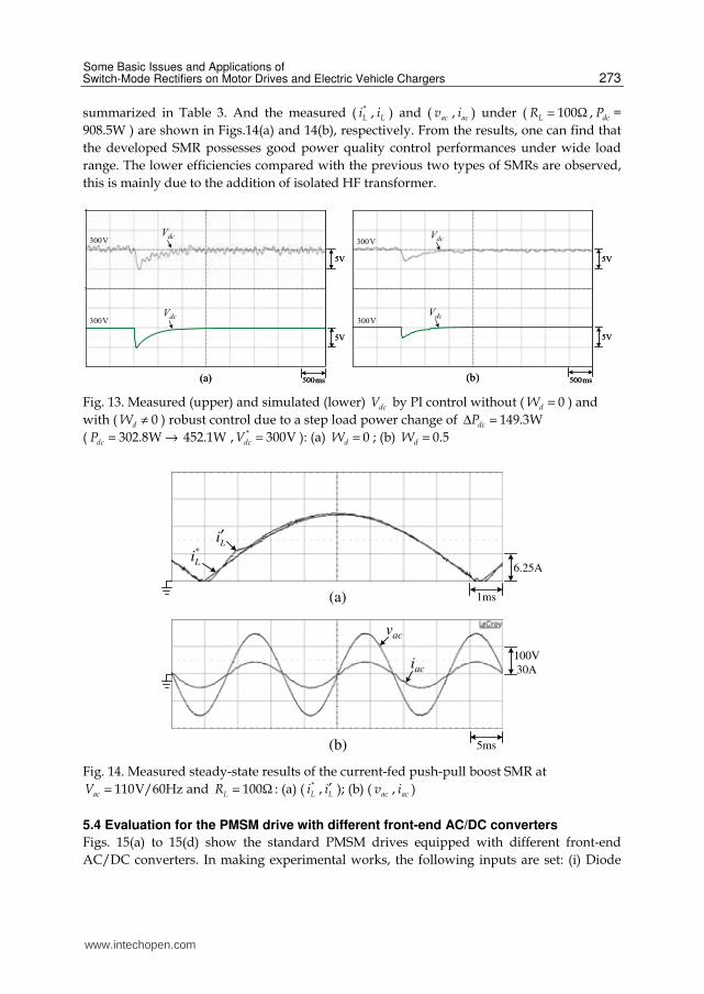
summarized in Table 3. And the measured ( *Li , Li ) and ( acv , aci ) under ( 100ΩLR = , dcP =
908.5W ) are shown in Figs.14(a) and 14(b), respectively. From the results, one can find that
the developed SMR possesses good power quality control performances under wide load
range. The lower efficiencies compared with the previous two types of SMRs are observed,
this is mainly due to the addition of isolated HF transformer.
5V
500ms
300VdcV
(a)
5V
300V dcV
5V
300VdcV
5V
500ms
300VdcV
(b)
5V
500ms
300VdcV
(a)
5V
300V dcV
5V
300VdcV
5V
500ms
300VdcV
(b)
Fig. 13. Measured (upper) and simulated (lower) dcV by PI control without ( 0dW = ) and
with ( 0dW ≠ ) robust control due to a step load power change of 149.3WdcPΔ =
( 302.8WdcP = → 452.1W , * 300VdcV = ): (a) 0dW = ; (b) 0.5dW =
6.25A
1ms
Li′*
Li
(a)
5ms
100V
30A
acv
aci
(b)
Fig. 14. Measured steady-state results of the current-fed push-pull boost SMR at
110V/60HzacV = and 100ΩLR = : (a) ( *Li , Li′ ); (b) ( acv , aci )
5.4 Evaluation for the PMSM drive with different front-end AC/DC converters
Figs. 15(a) to 15(d) show the standard PMSM drives equipped with different front-end
AC/DC converters. In making experimental works, the following inputs are set: (i) Diode
www.intechopen.com

Electrical Generation and Distribution Systems and Power Quality Disturbances
274
rectifier: 220V/60HzacV = , dcV will vary with loading conditions; (ii) SMRs:
110V/60HzacV = , 300VdcV = with satisfactory regulation control, the switching frequency
25kHzsf = is set. The measured results are summarized as follows:
PMSG
LP
LR
Dynamic loadsL
sL
sL
sr
sr
sr
ase
bse
cse
PMSM
asi
bsi
csi
n
N
dcV
LT
eT rω
1T 3T 5T
4T 6T 2Tc
b
aaci
acv
acP
dC
dcP
ECEncodersignals
PMSG
LP
LR
Dynamic loadsL
sL
sL
sr
sr
sr
ase
bse
cse
PMSM
asi
bsi
csi
n
N
dcV
LT
eT rω
1T 3T 5T
4T 6T 2T
di
c
b
a
L D
S
si
Li
aci
acv
Standard boost SMR front-end
acP
dC
dcP
ECEncodersignals
(a)
(b)
PMSG
LP
LR
Dynamic loadsL
sL
sL
sr
sr
sr
ase
bse
cse
PMSM
asi
bsi
csi
n
N
dcV
LT
eT rω
1T 3T 5T
4T 6T 2T
c
b
a
dC
dcP
ECEncodersignals
aci
acv
acP
Li0.5L
0.5L
1S 2S
Bridgeless boost SMR front-end
di
(c)
dCdcV
L
sp NN :
2S
1S
mL
mL
Lv
1D 2D
3D 4D
aC
4S
3S
acv
aci
LiacP
PMSG
LP
LR
Dynamic loadsL
sL
sL
sr
sr
sr
ase
bse
cse
PMSM
asi
bsi
csi
n
N
LT
eT rω
1T 3T 5T
4T 6T 2Tc
b
a
dcP
ECEncodersignals
Current-fed push-pull boost SMR front -end
(d)
Fig. 15. The circuit configuration of established standard PMSM drive with SMR front-end: (a) diode rectifier front-end; (b) standard boost SMR front-end; (c) bridgeless boost SMR front-end; (d) current-fed push-pull boost SMR front-end
www.intechopen.com

Some Basic Issues and Applications of Switch-Mode Rectifiers on Motor Drives and Electric Vehicle Chargers
275
Load Cases
Variables
Resistive load
( 400ΩLR = )
Resistive load
( 200ΩLR = )
Resistive load
( 133ΩLR = )
Resistive load
( 100ΩLR = )
acV 110V/60Hz 110V/60Hz 110V/60Hz 110V/60Hz
acP 298.6W 557.4W 697.4W 1082.2W
dcV 301.2V 300.8V 300.5V 300.3V
dcP 234.6W 465.8W 623.8W 908.5W
η 78.57% 83.57% 89.45% 83.95%
iTHD 8.83% 6.62% 6.53% 3.82%
PF (Lagging) 0.997 0.998 0.998 0.998
Table 3. Measured characteristics of the current-fed push-pull boost SMR under four loads
5.4.1 Diode rectifier front-end
The measured ( *rω , rω ), ( AH , *
asi , asi′ ) and ( acv , aci ) at ( * 2000rpmrω = , 44.7ΩLR = ) and
( * 3000rpmrω = , 44.7ΩLR = ) are shown in Fig. 16(a) and Fig. 16(b), and the corresponding
steady-state characteristics are listed in Table 4. One can notice the normal operation of the
PMSM drive under * 2000rpmrω = . However, the results in Fig. 16(b) indicate that large
tracking errors exist in speed and phase current under * 3000rpmrω = . This is mainly due to
the insufficient DC-link voltage ( 278.4VdcV = ) established by rectifier for encountering the
back-EMF effect. In addition, the peaky aci leads to poor power factor and high iTHD .
5ms
4A
AH
asi′*asi
5ms
100rpm2000rpm
*rω rω
200V
10A
acv
aci
(a) 5ms
5ms
4A
AH
asi′
*asi
5ms
100rpm
3000rpm
*rω
rω
200V
10A
acv
aci
(b) 5ms
Fig. 16. Measured ( *rω , rω ),( AH , *
asi , asi′ ) and ( acv , aci ) of the standard PMSM drive with
diode rectifier front-end at: (a) ( 220V/60HzacV = , * 2000rpmrω = , 44.7ΩLR = );
(b): ( 220V/60HzacV = , * 3000rpmrω = , 44.7ΩLR = )
www.intechopen.com

Electrical Generation and Distribution Systems and Power Quality Disturbances
276
Cases
Variables
* 2000rpmrω = * 3000rpmrω =
acV 220V/60Hz 220V/60Hz
acP 527.5W 969.4W
dcV 295.9V 278.4V
dcP 366.7W 706.3W
η 69.52% 72.86%
iTHD 72.95% 65.54%
PF (Lagging) 0.751 0.758
Table 4. Measured characteristics of the standard PMSM drive fed by diode rectifier front-
end under two speeds ( 220V/60HzacV = , 44.7ΩLR = )
5.4.2 Three boost SMR front-ends (i) Standard boost SMR: Fig. 17(a), Fig. 17(b) and Table 5; (ii) Bridgeless boost SMR: Fig. 18(a), Fig. 18(b) and Table 6; (iii) CFPP boost SMR: Fig. 19(a), Fig. 19(b) and Table 7. The results indicate that for all cases, the close winding current tracking performances are obtained, and thus good line drawn power quality characteristics are achieved. Further observations find that: (i) the efficiencies of bridgeless SMR are slightly higher than those of standard boost SMR; (ii) the efficiencies of the CFPP SMR are lower than the other two SMRs. This is mainly due to the increased losses in the high-frequency transformer.
Fig. 20(a) and Fig. 20(b) show the measured ( *rω , rω ), ( *
qsi , qsi′ ) and dcV of the whole PMSM
drive with CFPP boost SMR front-end at ( 300VdcV = , rω = 2400rpm, 44.7ΩLR = ) due to a
step speed command change of 100rpm and due to a step load resistance change from
75ΩLR = to 44.7ΩLR = . The results indicate that good speed tracking and regulating
responses are obtained by the developed SMR-fed PMSM drive. And the DC-link voltages
dcV are well regulated under these two cases.
100V
10A
acv
aci
5ms
5ms
4A
asi′*asi
(a)
100V
20A
acv
aci
5ms
5ms
4A
asi′*asi
(b)
Fig. 17. Measured ( *rω , rω ), ( AH , *
asi , asi′ ) and ( acv , aci ) of the standard PMSM drive with
standard boost SMR front-end at: (a) ( 220V/60HzacV = , * 2000rpmrω = , 44.7ΩLR = ); (b):
( 220V/60HzacV = , * 3000rpmrω = , 44.7ΩLR = )
www.intechopen.com

Some Basic Issues and Applications of Switch-Mode Rectifiers on Motor Drives and Electric Vehicle Chargers
277
Cases
Variables
* 2000rpmrω = * 3000rpmrω =
acV 110V/60Hz 110V/60Hz
acP 546.5W 1145.3W
dcV 300.6V 300.3V
dcP 365.9W 791.2W
η 66.95% 69.08%
iTHD 8.493% 7.085%
PF (Lagging) 0.998 0.997
Table 5. Measured characteristics of the standard PMSM drive fed by standard boost SMR
front-end under two speeds ( 300VdcV = , 44.7ΩLR = )
100V
10A
acv
aci
5ms
5ms
4A
asi′*asi
(a)
100V
20A
acv
aci
5ms
5ms
4A
asi′*asi
(b)
Fig. 18. Measured ( *rω , rω ), ( AH , *
asi , asi′ ) and ( acv , aci ) of the standard PMSM drive with
bridgeless boost SMR front-end at: (a) ( 220V/60HzacV = , * 2000rpmrω = , 44.7ΩLR = );
(b): ( 220V/60HzacV = , * 3000rpmrω = , 44.7ΩLR = )
Cases
Variables
* 2000rpmrω = * 3000rpmrω =
acV 110V/60Hz 110V/60Hz
acP 543.9W 1142.4W
dcV 300.4V 300.1V
dcP 364.8W 790.3W
η 67.07% 69.18%
iTHD 8.238% 7.022%
PF (Lagging) 0.998 0.996
Table 6. Measured characteristics of the standard PMSM drive fed by bridgeless boost SMR
front-end under two speeds ( 300VdcV = , 44.7ΩLR = )
www.intechopen.com

Electrical Generation and Distribution Systems and Power Quality Disturbances
278
4A
5ms
*asi
asi′
5ms
100V
10A
acv
aci
(a) (b)
4A
5ms
*asi asi′
5ms
100V
20A
acv
aci
Fig. 19. Measured ( *rω , rω ), ( AH , *
asi , asi′ ) and ( acv , aci ) of the standard PMSM drive with
current-fed push-pull SMR front-end at: (a) ( 220V/60HzacV = , * 2000rpmrω = , 44.7ΩLR = );
(b): ( 220V/60HzacV = , * 3000rpmrω = , 44.7ΩLR = )
CasesVariables
* 2000rpmrω = * 3000rpmrω =
acV 110V/60Hz 110V/60Hz
acP 597.8W 1231.8W
dcV 301.2V 300.7V
dcP 365.3W 792.1W
η 61.10% 64.30%
iTHD 3.90% 4.02%
PF (Lagging) 0.998 0.998
Table 7. Measured characteristics of the standard PMSM drive fed by current-fed push-pull
boost SMR front-end under two speeds ( 300VdcV = , 44.7ΩLR = )
10ms
50rpm2400rpm
2A
20ms
10V
100ms
300V
*rω
rω
*qsi
qsi′
dcV
(a)
200ms
50rpm
2400rpm rω
1A
50ms
*qsi qsi′
10V
500ms
300V dcV
(b)
Fig. 20. Measured ( *rω , rω ), ( *
qsi , qsi′ ) and dcV of the whole PMSM drive with current-fed
push-pull boost SMR front-end at ( 300VdcV = , * 2400rpmrω = , 44.7ΩLR = ): (a) due to a step
speed command change of 100rpm: (b) due to a step resistive load change from 75ΩLR = to
44.7ΩLR =
www.intechopen.com
Some Basic Issues and Applications of Switch-Mode Rectifiers on Motor Drives and Electric Vehicle Chargers
279
6. Some specific applications of Switch-Mode Rectifier
The applications of three types of single-phase SMRs as the AC-DC front-end converters of PMSM drives and their comparative evaluation have been introduced in the previous section. In this section, a SMR fed switched-reluctance motor (SRM), a SMR based electric vehicle battery charger and a flyback SMR based battery plug-in charger are presented to further comprehend the advantages of using SMR.
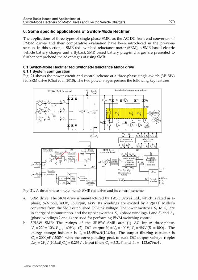
6.1 Switch-Mode Rectifier fed Switched-Reluctance Motor drive 6.1.1 System configuration Fig. 21 shows the power circuit and control scheme of a three-phase single-switch (3P1SW) fed SRM drive (Chai et al, 2010). The two power stages possess the following key features:
D
+
−
LR
SRM
AH BH
1W
1D 3D 2D
AD
AS
4S2S3S1SBD
BS 4D
dd pi ,
dCd
ovv =
1i
S
3P1SW SMR Front-end Switched reluctance motor drive
2i 3i 4i
rω
Hallsignals
2W 3W 4W
S
anv
cnv
n
fL
fL
fL
fC
fC
fC
bL1bi
2bi
3bi
bnvbL
bL
∑∗rω+
−
'rω
ωε
AS BS
41 ~ ii ′′cI
*4
*1 ~ ii
BH AH
2S 3S 4S1S2S 3S 4S1S
2S 3S 4S1S
DA /
2S 3S 4S1S
AS BS
Commutationlogic generator
Isolated gatedrivers
PIO
Random-band HCC
PWMschemes
Encorder interfacedtd /
rθffonosN θθ ,,
rθ
(Commutationtuning)
BH
AHBAEC ,
Speed control scheme
41 ~ ii ′′
SRM drive control scheme
Di
do RR =
abv
ai
bi
ci
PMSGEC
Phase winding current
commandgenerator
DSP
PWMmodulator
1cv
triv
ov′
*ov
Feedbackcontroller
cvG+−Σ
vεΣ
++
ahi
Notch filter
)(sHNF
se 180/1−bhi
chi
hi
−
+Σ
cv
chv
Three-phaserectifi-cation
Robust voltage control scheme
Robust current harmonic
compensation scheme
Robust error canceller
s/e 901−
)(swh
)(sH LFcv
LPF
*orv
*ov 1
)(swv
s
K
v
v
τ+1ov
ais
K
i
i
τ+1
A/D
A/D
Fig. 21. A three-phase single-switch SMR fed drive and its control scheme
a. SRM drive: The SRM drive is manufactured by TASC Drives Ltd., which is rated as 4-
phase, 8/6 pole, 400V, 1500rpm, 4kW. Its windings are excited by a 2(n+1) Miller’s
converter from the SMR established DC-link voltage. The lower switches 1S to 4S are
in charge of commutation, and the upper switches AS (phase windings 1 and 3) and BS
(phase windings 2 and 4) are used for performing PWM switching control.
b. 3P1SW SMR: The ratings of the 3P1SW SMR are: (1) AC input: three-phase,
LV = 220 ± 10% rmsV , 60Hz; (2) DC output: 400V,o dV V= = 4 ( 40 )o oP kW R= = Ω . The
energy storage inductor is 15.459 (10 )bL H kHzµ= . The output filtering capacitor is
2000 / 500oC F Vµ= with the corresponding peak-to-peak DC output voltage ripple:
2 /(105 ) 0.253o o o ov V R C VωΔ = = . Input filter: 3.3 FfC µ= and fL = 123.679 Hµ .
www.intechopen.com

Electrical Generation and Distribution Systems and Power Quality Disturbances
280
6.1.2 SMR control scheme The SMR control scheme shown in Fig. 21 consists of a robust current harmonic cancellation scheme and a robust voltage control scheme. The undesired line current and output voltage ripples are regarded as disturbances and they are reduced via robust controls. Owing to the boostable and regulated DC-link voltage provided by the SMR, the dynamic responses of the followed SRM drive are enhanced, and its vibration and speed ripple are also reduced. a. Robust current harmonic compensation scheme: The three-phase total current harmonic
current hi is synthesized from the sensed phase-a line current ai . Then an injected PWM robust compensating control voltage ( )ch h hv w s i= is yielded, where ( )hw s denotes a robust harmonic compensation weighting function.
b. Robust voltage control scheme: A compensation control command * ( )or v vv w s ε= is generated from the tracking error vε . The weighting factor in the weighting function
( )vw s is updated according to load level, which is identified from the low-pass filtered control voltage ( )c LF cv H s v= . The chaotic phenomena can be avoided automatically, better SMR control performance and voltage response are obtained simultaneously.
6.1.3 Performance evaluation
The SMR fed SRM drive is shown in Fig. 21. At the operation condition of ( 400dV V= , 1500rpmrω = , 13.2ΩLR = , 2135dP W= ), the measured DC-link voltages ( )dv t and vibrations ( )a t using different AC/DC front-end converters are compared in Figs. 22(a) and 22(b). The results show that the DC-link voltage ripple and the stator vibration using conventional rectifier as a front-end (measured line power quality parameters are 0.631,PF = 134%iTHD = ) are slightly reduced by employing the three-phase SMR ( 1hW = ) with PI control only ( 0vW = )( 0.953,PF = 18.82%iTHD = ). Larger performance improvement is achieved by applying the robust voltage control scheme with the weighting factor being automatically set to be 0.989vW = . The results in Figs. 22(a) and 22(b) ( 0.968,PF = 10.33%iTHD = ) indicate the further improvements both in DC-link voltage ripple and stator vibration.
)(ta
1ms
2/98.0
sm
)(tvd
1V
2ms
400V
400V
400V
Rectifier+SRM
(a)
(b)
SMR (PI and robust control s) + SRM
SMR((PI control only)+SRM
SMR (PI and robust control s) + SRM
Rectifier+SRM
SMR((PI control only)+SRM
Fig. 22. Measured DC-link voltages ( )dv t and vibrations ( )a t of the SRM drive fed by different AC/DC front-end converters at ( 400 ,dV V= 1500 ,r rpmω = , 13.2ΩLR = ,
2135dP W= (a) ( )dv t ; (b) ( )a t
www.intechopen.com

Some Basic Issues and Applications of Switch-Mode Rectifiers on Motor Drives and Electric Vehicle Chargers
281
At three cases of ( 1500r rpmω = , 13.2ΩLR = , 2135dP W= ), ( 1000r rpmω = , 22ΩLR = ,
1396dP W= ) and ( 100r rpmω = , 3.4ΩLR = , 807dP W= ), and the SMR robust voltage control
scheme and the SRM drive control schemes are normally operated, the measured power
quality characteristics of the established SMR without ( 0hW = ) and with ( 1.0hW = ) current
harmonic compensation are listed in Table 8.The results show that the fundamental and all
other harmonic currents are all reduced and the efficiency of the SMR is increased
accordingly by the harmonic compensation approach. Moreover, the line drawn power
quality improvements at all cases are also obtained.
2.135 , 1500 , 13.2d r LP kW rpm Rω= = = Ω
PF acP
(kW)
THDi (%)
Ia1
(Arms)Ia5
(Arms)Ia7
(Arms)Ia11
(Arms) Efficiency
(%)
0hW = 0.953 2.414 18.82 5.18 0.81 0.55 0.08 88.44
1.0hW = 0.968 2.362 10.33 5.01 0.42 0.31 0.04 90.39
1.396 , 1000 , 22d r LP kW rpm Rω= = = Ω
0hW = 0.941 1.598 19.13 3.58 0.62 0.29 0.05 87.36
1.0hW = 0.951 1.579 11.01 3.03 0.28 0.18 0.04 88.41
0.807 , 100 , 3.4d r LP kW rpm Rω= = = Ω
0hW = 0.935 0.959 23.47 2.16 0.44 0.25 0.08 84.15
1.0hW = 0.943 0.932 19.54 1.91 0.33 0.17 0.06 86.59
Table 8. The measured power quality characteristics under SRM drive active load at various power levels without and with current harmonic compensation
6.2 Switch-Mode Rectifier based EV battery charger 6.2.1 System configuration
A battery powered SRM drive for electric vehicle propulsion is shown in Fig. 23(a) (H.C.
Chang & Liaw, 2009). In driving mode, the switches are set as: mS → M and dS → closed.
The SRM (DENSEI company Japan) is rated as 4-phase, 8-6, 48V, 6000rpm, 2.3kW. The
components , ,b b bS D L and dC in Fig. 23(a) form a DC/DC boost converter. The nominal
battery voltage is 12 4 48VbV = × = , it is boosted and establishes the DC-link voltage with
48V 72V.daV≤ ≤ During demagnetization of each communication stroke, the winding
energies can be directly sent back to the battery bank via the diodes 1 3 5, ,D D D and 7D .
In charging mode, the switches in Fig. 23(a) are set as: mS → C and dS permanently off.
With the insertion of off-board part, a buck-boost SMR based charger is formed and drawn
in Fig. 23(b) with the employed embedded motor drive components being highlighted. The
diode eD is added to avoid the short circuit of battery when 6Q is turned on. The
inductances of the first two motor windings are used as the input filter components during
each half AC cycle. And the third motor winding inductance is employed as the energy
storage component of the SMR.
The SMR control scheme shown in Fig. 23(b) consists of outer charging control scheme and
inner current controlled PWM scheme. Initially, the battery is charged in constant current
www.intechopen.com

Electrical Generation and Distribution Systems and Power Quality Disturbances
282
mode to let the batteries be charged under maximum current (0.25C/9.5A) until the
condition of 52V ( 13V 4)bV ≥ = × reaches. Then the charging enters constant voltage
floating mode.
5D
dC+
−bS
bv
A′
acv
fC
aci
Batterybank
Utilitysource
mSM
C
i
LR
C
PMSG
C
SRM and converter
Test load
On-boar
Off-board
5D
dCd+
−bSbbv
A′Batttt eryrrbank
y
mSmM
C
i
LR
C
PMSG
C
SRM and convertrr er
Test load
On-nn boar
1Q 3Q 5Q
2Q4Q
(a)
)(
3iiL
1L
acv+
−fC
2D
1D 3D
4D
bCbv
2L
)(3
LL
)(EB
)(BE A
)(6
SQ
B′
A′
)(6
DD
aci
)(DDe
Buck/boost PFC charger
Embedded components of SRM and converter
acP
cbP
(b)
)ON(5Q
bi Di
Di
Σ
∗
Li)( 6Q
v pwm
)(ts
acv
Currentcontroller
Li′
iε
)(sWib
Σ
∗
1Li
∗
Lci
PWM
A/D A/D
bv
bv′
DSP TMS320F240
∗
bvΣ
Lm
cI
I =)(sGcv
Voltagecontroller
bv′
N
YAIc 71.22=
Vvb
52≤′bv′
Reference signal
generator
XINTBattery charging control scheme
SMR current control scheme
)( 3iiL
icK vcK
)(sGib
Fig. 23. A battery powered SRM drive with voltage boosting for electric vehicle propulsion: (a) system configuration; (b) schematic and control scheme of the formed on-board buck-boost SMR based battery charger in idle status
www.intechopen.com

Some Basic Issues and Applications of Switch-Mode Rectifiers on Motor Drives and Electric Vehicle Chargers
283
6.2.2 Performance evaluation
The derivation of circuit component ratings and the implementation affairs of the SRM drive
shown in Fig. 23(a) and Fig. 23(b) can be referred to (H.C. Chang & Liaw, 2009). Some
results concerning charging mode are observed here. Under the constant current charging
mode with 21.3ALm cI I= = and switching frequency 12.5sf kHz= , the measured Li and its
command *Li by PI control and robust control ( ibW = 0.85) are shown in Fig. 24(a)
( 47.65V , 9.45Ab bv I= = ). The close inductor current tracking control is observed from the
results. Fig. 24(b) shows the corresponding AC source voltage acv and current aci (PF =
0.989, iTHD = 4.23 %). Good line drawn waveform and power quality by the buck-boost
SMR charger can be seen from the results.
To observe the effects of switching frequency on the SMR control performance, Table 9 lists
measured performance parameters corresponding to the switching frequencies
of 12.5 ,sf kHz= 15kHz , 7.5kHz and 2.5kHz ( 0.85ibW = ). Some facts are observed from the
results: (i) The current loop is normally operated at each switching frequency; and (ii) As the
switching frequency becomes smaller, the inductor current will gradually become partial
and then total discontinuous current mode (DCM) within the AC cycle. Accordingly, the
power quality becomes worse.
10A
1ms(a)
10A
5ms(b)
100V
aci
acv 85.0=ibW
*Li
controls)feedback robust and PI( 85.0=ibW
Li
kHzfs 5.12=
Fig. 24. Measured results of the buck-boost SMR based charger in constant-current charging
mode at ( 47.65V , 9.45Ab bv I= = ): (a) Li and *Li by PI and robust controls
( 0.85ibW = , 12.5sf kHz= ); (b) acv and aci (PF=0.989, iTHD =4.23%)
sf Variables
kHz.52 kHz.57 kHz.512 kHz15
(W)acP 579.7 563.4 547.8 560.6
(A)acI 5.56 5.15 5.11 5.14
(W)bP 388.4 427.3 453.3 459.4
(V)bV 46.32 47.12 47.65 47.73
(A)bI 8.22 9.02 9.45 9.45
(%)η 67.00 75.84 82.75 81.95
PF 0.972 0.981 0.989 0.991
(%)aciTHD 10.02 7.84 4.23 4.04
Table 9. Measured power quality parameters of the buck-boost SMR based charger under different switching frequencies
www.intechopen.com
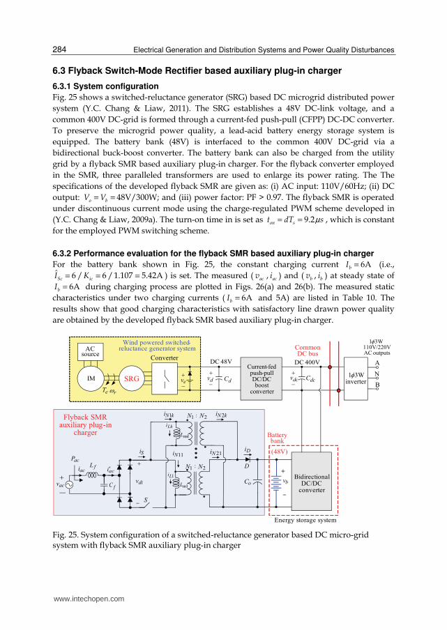
Electrical Generation and Distribution Systems and Power Quality Disturbances
284
6.3 Flyback Switch-Mode Rectifier based auxiliary plug-in charger
6.3.1 System configuration
Fig. 25 shows a switched-reluctance generator (SRG) based DC microgrid distributed power
system (Y.C. Chang & Liaw, 2011). The SRG establishes a 48V DC-link voltage, and a
common 400V DC-grid is formed through a current-fed push-pull (CFPP) DC-DC converter.
To preserve the microgrid power quality, a lead-acid battery energy storage system is
equipped. The battery bank (48V) is interfaced to the common 400V DC-grid via a
bidirectional buck-boost converter. The battery bank can also be charged from the utility
grid by a flyback SMR based auxiliary plug-in charger. For the flyback converter employed
in the SMR, three paralleled transformers are used to enlarge its power rating. The The
specifications of the developed flyback SMR are given as: (i) AC input: 110V/60Hz; (ii) DC
output: o bV V= = 48V/300W; and (iii) power factor: PF > 0.97. The flyback SMR is operated
under discontinuous current mode using the charge-regulated PWM scheme developed in
(Y.C. Chang & Liaw, 2009a). The turn-on time in is set as 9.2on st dT sµ= = , which is constant
for the employed PWM switching scheme.
6.3.2 Performance evaluation for the flyback SMR based auxiliary plug-in charger
For the battery bank shown in Fig. 25, the constant charging current 6AbI = (i.e., ˆ 6 / 6 /1.107 5.42ASc icI K= = = ) is set. The measured ( acv , aci ) and ( bv , bi ) at steady state of
6AbI = during charging process are plotted in Figs. 26(a) and 26(b). The measured static
characteristics under two charging currents ( 6AbI = and 5A) are listed in Table 10. The
results show that good charging characteristics with satisfactory line drawn power quality
are obtained by the developed flyback SMR based auxiliary plug-in charger.
IM SRG
ACsource
rωeT
Wind powered switched-reluctance generator system
Converter
+
−dCdv
Current-fedpush-pullDC/DC boost
converter
+
−dcCdcv
BidirectionalDC/DC
converter
ev+
−
Energy storage system
48V DC 400V DC
Common DC bus outputs AC
110V/220V3W1 φ
inverterW31 φ
A
B
N
bv1mL
:
mkL
D
oC
Di
S
Lki
1Li
Si
kNi 1
11Ni
kNi 2
21Ni
1N 2N
:1N 2N
−
cai′
fCacv+
−
aci
acP
div
+fL
Battery bank
(48V)
Flyback SMR auxiliary plug-in
charger
Fig. 25. System configuration of a switched-reluctance generator based DC micro-grid system with flyback SMR auxiliary plug-in charger
www.intechopen.com
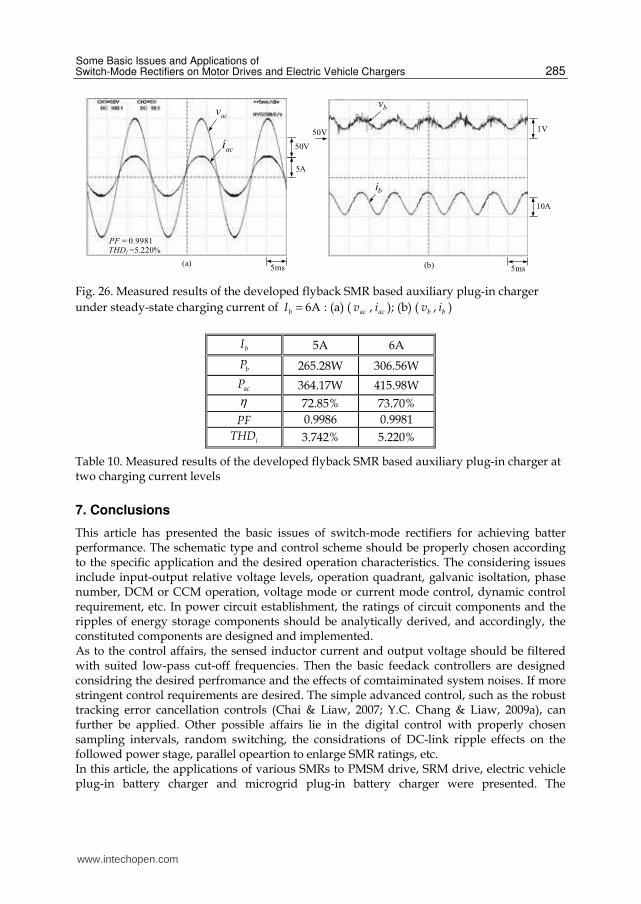
Some Basic Issues and Applications of Switch-Mode Rectifiers on Motor Drives and Electric Vehicle Chargers
285
acv
aci
5ms
5A
50V
PF = 0.9981THDi =5.220%
(a)
bv
bi
1V
10A
50V
5ms(b)
Fig. 26. Measured results of the developed flyback SMR based auxiliary plug-in charger
under steady-state charging current of 6AbI = : (a) ( acv , aci ); (b) ( bv , bi )
bI 5A 6A
bP 265.28W 306.56W
acP 364.17W 415.98W
η 72.85% 73.70%
PF 0.9986 0.9981
iTHD 3.742% 5.220%
Table 10. Measured results of the developed flyback SMR based auxiliary plug-in charger at two charging current levels
7. Conclusions
This article has presented the basic issues of switch-mode rectifiers for achieving batter performance. The schematic type and control scheme should be properly chosen according to the specific application and the desired operation characteristics. The considering issues include input-output relative voltage levels, operation quadrant, galvanic isoltation, phase number, DCM or CCM operation, voltage mode or current mode control, dynamic control requirement, etc. In power circuit establishment, the ratings of circuit components and the ripples of energy storage components should be analytically derived, and accordingly, the constituted components are designed and implemented. As to the control affairs, the sensed inductor current and output voltage should be filtered with suited low-pass cut-off frequencies. Then the basic feedack controllers are designed considring the desired perfromance and the effects of comtaiminated system noises. If more stringent control requirements are desired. The simple advanced control, such as the robust tracking error cancellation controls (Chai & Liaw, 2007; Y.C. Chang & Liaw, 2009a), can further be applied. Other possible affairs lie in the digital control with properly chosen sampling intervals, random switching, the considrations of DC-link ripple effects on the followed power stage, parallel opeartion to enlarge SMR ratings, etc. In this article, the applications of various SMRs to PMSM drive, SRM drive, electric vehicle plug-in battery charger and microgrid plug-in battery charger were presented. The
www.intechopen.com

Electrical Generation and Distribution Systems and Power Quality Disturbances
286
treatments of basic issues in power circuit and control scheme have been decribed. And their comparative performances have also been assessed to demonstrate the effectiveness of the introduced issues. It is believed that the cost-effective SMR fed power palnt with satisfactory performance can be achieved if the suggested basic issues can be considered.
8. References
Backman, N. & Wolpert, T. (2000). Simplified Single Stage PFC Including Peak Current Mode Control in a Flyback Converter, Proceedings of IEEE Telecommunications Energy Conference, pp. 317-324, ISBN 0-7803-6407-4
Badin, A. A. & Barbi, I. (2008). Unity Power Factor Isolated Three-Phase Rectifier with Split DC-Bus Based on the Scott Transformer. IEEE Transactions on Power Electronics, Vol.23, No.3, (May 2008), pp. 1278-1287, ISSN 0885-8993
Buso, S.; Spiazzi, G. & Tagliavia, D. (2000). Simplified Control Technique for High-Power-Factor Flyback Cuk and Sepic Rectifiers Operating in CCM. IEEE Transactions on Industry Applications, Vol.36, No.5, (September 2000), pp. 1413-1418, ISSN 0093-9994
Chai, J. Y. & Liaw, C. M. (2007). Robust Control of Switch-Mode Rectifier Considering Nonlinear Behavior. IET Electric Power Applications, Vol.1, No.3, (May 2007), pp. 316-328, ISSN 1751-8660
Chai, J. Y.; Ho, Y. H.; Chang, Y. C. & Liaw, C. M. (2008). On Acoustic Noise Reduction Control Using Random Switching Technique for Switch-Mode Rectifiers in PMSM Drive. IEEE Transactions on Industrial Electronics, Vol.55, No.3, (March 2008), pp. 1295-1309, ISSN 0278-0046
Chai, J. Y. & Liaw, C. M. (2009). Development Of a Switched-Reluctance Motor Drive with PFC Front-End. IEEE Transactions on Energy Conversion, Vol.24, No.1, (March 2009), pp. 30-42, ISSN 0885-8969
Chai, J. Y.; Chang, Y. C. & Liaw, C. M. (2010). On the Switched-Reluctance Motor Drive with Three-Phase Single-Switch-Mode Rectifier Front-End. IEEE Transactions on Power Electronics, Vol.25, No.5, (May 2010), pp. 1135-1148, ISSN 0885-8993
Chang, H. C. & Liaw, C. M. (2009). Development of a Compact Switched-Reluctance Motor Drive for EV Propulsion with Voltage Voosting and PFC Charging Capabilities. IEEE Transactions on Vehicular Technology, Vol.58, No.7, (March 2009), pp. 3198-3215, ISSN 0018-9545
Chang, Y. C. & Liaw, C. M. (2009). Design and Control for a Charge-Regulated Flyback Switch-Mode Rectifier. IEEE Transactions on Power Electronics, Vol.24, No.1, (January 2009), pp. 59-74, ISSN 0885-8993
Chang, Y. C. & Liaw, C. M. (2009). Development and Control of a Flyback Switch-Mode Rectifier with Enlarged Rating via Paralleled Transformers, Proceedings of Taiwan Power Electronics Conference and Exhibition, pp. 1287-1293
Chang, Y. C. & Liaw, C. M. (2011). A Flyback Rectifier with Spread Harmonic Spectrum. IEEE Transactions on Industrial Electronics, to appear in No.99, ISSN 0278-0046
Chen, H. C.; Li, S. H. & Liaw, C. M. (2004). Switch-Mode Rectifier with Digital Robust Ripple Compensation and Current Waveform Controls. IEEE Transactions on Power Electronics, Vol.19, No.2, (March 2004), pp. 560-566, ISSN 0885-8993
Das, P. & Moschopoulos, G. (2007). A Comparative Study of Zero-Current-Transition PWM Converters. IEEE Transactions on Industrial Electronics, Vol.54, No.3, (June 2007), pp. 1319-1328, ISSN 0278-0046
www.intechopen.com

Some Basic Issues and Applications of Switch-Mode Rectifiers on Motor Drives and Electric Vehicle Chargers
287
Dawande, M. S. & Dubey, G. K. (1996). Single-Phase Switch Mode Rectifiers, Proceedings of IEEE Power Electronics, Drives and Energy Systems for Industrial Growth, pp. 637-642, ISBN 0-7803-2795-0
Erickson, R. & Madigan, M. (1990). Design of a Simple High-Power-Factor Rectifier Based on the Flyback Converter, Proceedings of IEEE Applied Power Electronics Conference and Exposition, pp. 792-801,
Erickson, R. W. & Maksimovic, D. (2001). Fundamentals of Power Electronics (2nd), Kluwer Academic Publishers, ISBN 0-7923-7270-0, Norwell Massachusetts
Farcas, C.; Petreus, D.; Simion, E.; Palaghita, N. & Juhos, Z. (2006). A Novel Topology Based on Forward Converter with Passive Power Factor Correction, Proceedings of International Spring Seminar on Electronics Technology, pp. 268-272, ISBN 1-4244-0551-3
Forest, F.; Laboure, E.; Meynard, T. A. & Huselstein, J. J. (2007). Multicell Interleaved Flyback Using Intercell Transformers. IEEE Transactions on Power Electronics, Vol.22, No.5, (September 2007), pp. 1662-1671, ISSN 0885-8993
Forest, F.; Laboure, E.; Gelis, B.; Smet, V.; Meynard, T. A. & Huselstein, J. J. (2009). Design of Intercell Transformers for High-Power Multicell Interleaved Flyback Converter. IEEE Transactions on Power Electronics, Vol.24, No.3, (March 2009), pp. 580-591, ISSN 0885-8993
Gataric, S.; Boroyevich, D. & Lee, F. C. (1994). Soft-Switched Single-Switch Three-Phase Rectifier with Power Factor Correction, Proceedings of IEEE Applied Power Electronics Conference and Exposition, pp. 738-744, ISBN 0-7803-1456-5
Hahn, J.; Enjeti, P. N. & Pitel, I. J. (2002). A New Three-Phase Power Factor Correction (PFC) Scheme Using Two Single-Phase PFC Modules. IEEE Transactions on Industry Applications, Vol.38, No.1, (October 2002), pp. 123-130, ISSN 0093-999
Hengchun, M.; Lee, F. C.; Boroyevich, D. & Hiri, S. (1997). Review of High Performance Three-Phase Power-Factor Correction Circuits. IEEE Transactions on Industrial Electronics, Vol.44, No.4, (August 1997), pp. 437-446, ISSN 0278-0046
Hsieh, Y. H. (2010) Position Sensorless Permanent-Magnet Synchronous Motor Drive with Switch-Mode Rectifier Front-End, Master Thesis, Department of Electrical Engineering, National Tsing Hua University, Taiwan, ROC
Huber, L.; Jang, Y. & Jovanovic, M. M. (2008). Performance Evaluation of Bridgeless PFC Boost Rectifiers. IEEE Transactions on Power Electronics, Vol.23, No.3, (February 2008), pp. 1381-1390, ISSN 1048-2334
Inoue, T.; Hamamura, S.; Yamamoto, M.; Ochi, A. & Sasaki, Y. (2008). AC-DC Converter Based on Parallel Drive of Two Piezoelectric Transformers. Japanese Journal of Applied Physics, Vol.47, No.5, (May 2008), pp. 4011-4014, ISSN 0021-4922
Jang, Y.; Dillman, D. L. & Javanovic, M. M. (2006). A New Soft-Switched PFC Boost Rectifier with Integrated Flyback Converter for Stand-By Power. IEEE Transactions on Power Electronics, Vol.21, No.1, (January 2006), pp. 66-72, ISSN 0885-8993
Kwon, J. M.; Kim, E. H.; Kwon, B. H. & Nam, K. H. (2008). High Efficiency Fuel Cell Power Conditioning System with Input Current Ripple Reduction. IEEE Transactions on Industrial Electronics, Vol.56, No.3, (March 2009), pp. 826-834, ISSN 0278-0046
Lamar, D. G.; Fernandez, A.; Arias, M.; Rodriguez, M.; Sebastian, J. & Hernando, M. M. (2007). Limitations of the Flyback Power Factor Corrector as a One-Stage Power
www.intechopen.com

Electrical Generation and Distribution Systems and Power Quality Disturbances
288
Supply, Proceedings of IEEE Power Electronics Specialists Conference, pp. 1343-1348, ISBN 0275-9306
Langeslag, W.; Pagano, R.; Schetters, K.; Strijker, A. & Zoest, A. (2007). VLSI Design and Application of A High-Voltage-Compatible SoC–ASIC in Bipolar CMOS/DMOS Technology for AC–DC Rectifiers. IEEE Transactions on Industrial Electronics, Vol.54, No.5, (October 2007), pp. 2626-2641, ISSN 0278-0046
Larouci, C.; Ferrieux, J. P.; Gerbaud, L.; Roudet, J. & Barbaroux, J. (2002). Control of a Flyback Converter in Power Factor Correction Mode: Compromise Between the Current Constraints and the Transformer Volume, Proceedings of IEEE Applied Power Electronics Conference and Exposition, Vol.2, pp. 722-727, ISBN 0-7803-7404-5
Lee, J. J.; Kwon, J. M.; Kim, E. H.; Choi, W. Y. & Kwon, B. H. (2008). Single-Stage Single-Switch PFC Flyback Converter Using a Synchronous Rectifier. IEEE Transactions on Industrial Electronics, Vol.55, No.3, (March 2008), pp. 1352-1365, ISSN 0278-0046
Li, S. H. & Liaw, C. M. (2003). Modelling and Quantitative Direct Digital Control for a DSP-Based Soft-Switching-Mode Rectifier. IEE Proceedings of Electric Power Applications, Vol.150, No.1, (January 2003), pp. 21-30, ISSN 1350-2352
Li, S. H. & Liaw, C. M. (2004). Paralleled DSP-based Soft Switching-Mode Rectifiers with Robust Voltage Regulation Control. IEEE Transactions on Power Electronics, Vol.19, No.4, (July, 2004), pp. 937-946, 0885-8993
Li, S. H. & Liaw, C. M. (2004). On the DSP-Based Switch-Mode Rectifier with Robust Varying-Band Hysteresis PWM Scheme. IEEE Transactions on Power Electronics, Vol.19, No.6, (November, 2004), pp. 1417-1425, ISSN 0885-8993
Li, S. H.; & Liaw, C. M. (2004). Development of Three-Phase Switch-Mode Rectifier Using Single-Phase Modules. IEEE Transactions on Aerospace and Electronic Systems, Vol.40, No.1, (January 2004), pp. 70-79, ISSN 0018-9251
Liaw, C. M.; Lin, Y. M.; Wu, C. H. & Hwy, K. I. (2000). Analysis, Design and Implementation of a Random Rrequency PWM Inverter. IEEE Transactions on Power Electronics, Vol.15, No.5, (September 2000), pp. 843-854, ISSN 0885-8993
Lu, D. D.; Cheng, D. K. & Lee, Y. S. (2003). Single-Switch Flyback Power-Factor-Corrected Ac/dc Converter with Loosely Regulated Intermediate Storage Capacitor Voltage, Proceedings of 2003 International Symposium on Circuits and Systems, pp. 264-267, ISBN 0-7803-7761-3
Lu, D. D.; Iu, H. H.; & Pjevalica, V. (2008). A Single-Stage AC/DC Converter with High Power Factor, Regulated Bus Voltage, and Output Voltage. IEEE Transactions on Power Electronics, Vol.23, No.1, (January 2008), pp. 218-228, ISSN 0885-8993
Mahdavi, M. & Farzanehfard, H. (2009). Zero-Current-Transition Bridgeless PFC without Extra Voltage and Current Stress. IEEE Transactions on Industrial Electronics, Vol.56, No.7, (July 2009), pp. 2540-2547, ISSN 0278-0046
Manh, D. C. & Guldner, H. (2006). High Output Voltage DC/DC Converter Based on Parallel Connection of Piezoelectric Transformers, Proceedings of International Symposium on Power Electronics, Electrical Drives, Automation and Motion, pp. 625-628, ISBN 1-4244-0193-3
Matsui, K.; Yamamoto, I; Kishi, T.; Hasegawa, M.; Mori, H. & Ueda, F. (2002). A Comparison Of Various Buck-Boost Converters and Their Application to PFC, Proceedings of IEEE 2002 28th Annual Conference of the Industrial Electronics Society, Vol.1, pp. 30-36, ISBN 0-7803-7474-6
www.intechopen.com
Some Basic Issues and Applications of Switch-Mode Rectifiers on Motor Drives and Electric Vehicle Chargers
289
Mishra, S. K.; Fernandes, B. G. & Chatterjee, k. (2004). Single Stage Single Switch AC/DC Converters with High Input Power Factor and Tight Output Voltage Regulation, Proceedings of IEEE 2004 30th Annual Conference of the Industrial Electronics Society, pp. 2690-2695, ISBN 0-7803-8730-9
Mohan, N.; Undeland, T. M. & Robbins, W. P. (2003). Power Electronics Converters, Applications and Design (3rd), John Wiley & Sons, ISBN 0-4712-2693-9, New York
Newsom, R. L.; Dillard W. C. & Nelms, R. M. (2002). Ditigal Power-Factor Correction for a Capacitor-Charging Power Supply. IEEE Transactions on Industrial Electronics, Vol.49, No.5, (October 2002), pp. 1146-1153, ISSN 0278-0046
Olivera, D. S.; Barreto, L.; Antunes, F.; Silva, M.; Queiroz, D. L. & Rangel, A. R. (2009). A DCM Three-Phase High Frequency Semi-Controlled Rectifier Feasible for Power WECS Based on a Permanent Magnet Generator, Proceedings of IEEE Power Electronics Conference, pp. 1193-1199, ISBN 2175-8603
Orabi, M. & Ninomiya, T. (2003). Nonlinear Dynamics of Power-Factor-Correction Converter. IEEE Transactions on Industrial Electronics, Vol.50, No.6, (December 2003), pp. 1116-1125, ISSN 0278-0046
Papanikolaou, P. N.; Tatakis, C. E. & Kyritsis, A. C. (2005). Design of a PFC AC/DC Flyback Converter for Low Voltage Applications, Proceedings of 2005 European Conference on Power Electronics and Applications, pp. 1-10, ISBN 90-75815-09-3
Reis, M. M.; Soares, B.; Barreto, L.; Freitas, E.; Silva, C. E. A.; Bascope, R. T. & Olivera, D. S. (2008). A Variable Speed Wind Energy Conversion System Connected to the Grid for Small Wind Generator, Proceedings of IEEE Applied Power Electronics Conference and Exposition, Vol.1, pp. 751-755, ISBN 1048-2334
Rikos, E. J. & Tatakis, E. C. (2005). Single-Stage Single-Switch Isolated PFC Converter with Non-Dissipative Clamping. IEE Proceedings Electric Power Applications, Vol.152, No.2, (March 2005), pp. 166-174, ISSN 1350-2352
Sangsun, K. & Enjeti, P. N. (2002). A Parallel-Connected Single Phase Power Factor Correction Approach with Improved Efficiency, Proceedings of IEEE Applied Power Electronics Conference and Exposition, Vol.1, pp. 263-269, ISBN 0-7803-7404-5
Sangwon, L. & Sewan, C. (2010). AThree-Phase Current-Fed Push-Pull DC-DC Converter with Active Clamp for Fuel Cell Applications, Proceedings of IEEE Applied Power Electronics Conference and Exposition, pp. 1934-1941, ISBN 978-1-4244-4782-4
Shah, J. & Moschopoulos, G. (2005). Three-Phase Rectifiers with Power Factor Correction, Proceedings of 2005 Canadian Conference on Electrical and Computer Engineering, pp. 1270-1273, ISBN 0-7803-8885-2
Singh, B.; Singh, B. P.; & Dwivedi, S. (2006). Performance Comparison of High Frequency Isolated AC-DC Converters for Power Quality Improvement at Input AC Mains, Proceedings of IEEE International Conference on Power Electronics, Drives and Energy Systems, pp. 1-6, ISBN 0-7803-9772-X
Singh, B. & Singh, S. (2010). Single-Phase Power Factor Controller Topologies for Permanent Magnet Brushless DC Motor Drives. IET Power Electronics, Vol.3, No.2, (March 2010), pp. 147-175, ISSN 1755-4535
Tang, W.; Jiang, Y. H.; Verghese, G. C. &Lee, F. C. (1993). Power Factor Correction with Flyback Converter Employing Charge Control, Proceedings of IEEE Applied Power Electronics Conference and Exposition, pp. 293-298, ISBN 0-7803-0983-9
www.intechopen.com
Electrical Generation and Distribution Systems and Power Quality Disturbances
290
Tanitteerapan, T. & Mori, S. (2001). An Input Current Shaping Technique for PFC Flyback Rectifier by Using Inductor Voltage Detection Control Method, Proceedings of IEEE Region 10 International Conference on Electrical and Electronic Technology, Vol.2, pp. 799-803, ISBN 0-7803-7101-1
Ting, Q. H. & Lehman,B. (2008). Coupled Input-Series and Output-Parallel Dual Interleaved Flyback Converter for High Input Voltage Application. IEEE Transactions on Power Electronics, Vol.23, No.1, (January, 2008), pp. 88-95, ISSN 0885-8993
Tse, K. K.; Chung, H. S. –H.; Hui, S. Y. R. & So, H. C. (2000). A Comparative Investigation on the Use of Random Modulation Schemes for DC/DC Converters. IEEE Transactions on Industrial Electronics, Vol.47, No.2, (April 2000), pp. 253-263, ISSN 0278-0046
Uan-Zo-li, A.; Lee, F. C. & Burgos, R. (2005). Modeling, Analysis and Control Design of Single-Stage Voltage Source PFC Converter, Proceedings of IEEE Industry Applications Conference, Vol.3, pp. 1684-1691, ISBN 0-7803-9208-6
Ueda, A.; Ito, Y.; Kurimoto, Y. & Torii, A. (2002). Boost Type Three-Phase Diode Rectifier Using Current Resonant Switch, Proceedings of IEEE Power Conversion Conference, Vol.1, pp. 13-18, ISBN 0-7803-7156-9
Wang, C. M. (2010) Development of Switched-Reluctance Motor Drive with Three-Phase Switch-Mode Rectifier Front-End, Master Thesis, Department of Electrical Engineering, National Tsing Hua University, Taiwan, ROC
Wang, K.; Lee, F. C. & Boroyevich (1994). Soft-Switched Single-Switch Three-Phase Rectifier with Power Factor Correction, Proceedings of IEEE Applied Power Electronics Conference and Exposition, pp. 738-744, ISBN 0-7803-1456-5
Wolfs, P. & Thomas, P. (2007). Boost Rectifier Power Factor Correction Circuits with Improved Harmonic and Load Voltage Regulation Responses, Proceedings of IEEE Power Electronics Specialists Conference, pp. 1314-1318, ISBN 0275-9306
Youssef, N. B. H.; Al-Haddad, K. & Kanaan, H. Y. (2008). Implementation of a New Linear Control Technique Based on Experimentally Validated Small-Signal Model of Three-Phase Three-Level Boost-Type Vienna Rectifier. IEEE Transactions on Industrial Electronics, Vol.55, No.4, (April 2008), pp. 1666-1676, ISSN 0278-0046
Zhang, R.; Lee, F. C. & Boroyevich, D. (2000). Four-Legged Three-Phase PFC Rectifier with Fault Tolerant Capability, Proceedings of IEEE Power Electronics Specialists Conference, Vol.1, pp. 359-364, ISBN 0275-9306
Zheng, Y. & Moschopoulos, G. (2006). Design Considerations for a New AC-DC Single Stage Flyback Converter, Proceedings of IEEE Applied Power Electronics Conference and Exposition, pp. 400-406, ISBN 0-7803-9547-6
www.intechopen.com

Electrical Generation and Distribution Systems and Power QualityDisturbancesEdited by Prof. Gregorio Romero
ISBN 978-953-307-329-3Hard cover, 304 pagesPublisher InTechPublished online 21, November, 2011Published in print edition November, 2011
InTech EuropeUniversity Campus STeP Ri Slavka Krautzeka 83/A 51000 Rijeka, Croatia Phone: +385 (51) 770 447 Fax: +385 (51) 686 166www.intechopen.com
InTech ChinaUnit 405, Office Block, Hotel Equatorial Shanghai No.65, Yan An Road (West), Shanghai, 200040, China
Phone: +86-21-62489820 Fax: +86-21-62489821
The utilization of renewable energy sources such as wind energy, or solar energy, among others, is currentlyof greater interest. Nevertheless, since their availability is arbitrary and unstable this can lead to frequencyvariation, to grid instability and to a total or partial loss of load power supply, being not appropriate sources tobe directly connected to the main utility grid. Additionally, the presence of a static converter as output interfaceof the generating plants introduces voltage and current harmonics into the electrical system that negativelyaffect system power quality. By integrating distributed power generation systems closed to the loads in theelectric grid, we can eliminate the need to transfer energy over long distances through the electric grid. In thisbook the reader will be introduced to different power generation and distribution systems with an analysis ofsome types of existing disturbances and a study of different industrial applications such as battery charges.
How to referenceIn order to correctly reference this scholarly work, feel free to copy and paste the following:
C. M. Liaw and Y. C. Chang (2011). Some Basic Issues and Applications of Switch-Mode Rectifiers on MotorDrives and Electric Vehicle Chargers, Electrical Generation and Distribution Systems and Power QualityDisturbances, Prof. Gregorio Romero (Ed.), ISBN: 978-953-307-329-3, InTech, Available from:http://www.intechopen.com/books/electrical-generation-and-distribution-systems-and-power-quality-disturbances/some-basic-issues-and-applications-of-switch-mode-rectifiers-on-motor-drives-and-electric-vehicle-ch