solid-to-solid phase transformations of nanostructured
TRANSCRIPT

AIP Conference Proceedings 1603, 31 (2014); https://doi.org/10.1063/1.4883039 1603, 31
© 2014 AIP Publishing LLC.
Solid-to-solid phase transformations ofnanostructured selenium-tin thin filmsinduced by thermal annealing in oxygenatmosphereCite as: AIP Conference Proceedings 1603, 31 (2014); https://doi.org/10.1063/1.4883039Published Online: 17 February 2015
A. Serra, M. Rossi, A. Buccolieri, and D. Manno
ARTICLES YOU MAY BE INTERESTED IN
Temperature dependence of Raman shifts in layered ReSe2 and SnSe2 semiconductor
nanosheetsApplied Physics Letters 107, 013105 (2015); https://doi.org/10.1063/1.4926508
Few-layer SnSe2 transistors with high on/off ratios
Applied Physics Letters 108, 053506 (2016); https://doi.org/10.1063/1.4941394
SnSe2 field-effect transistors with high drive current
Applied Physics Letters 103, 263104 (2013); https://doi.org/10.1063/1.4857495

Solid-to-solid phase transformations of nanostructured Selenium-Tin thin films induced by thermal annealing in
oxygen atmosphere
A. Serraa, M. Rossib, A. Buccolieric and D. Mannoc
a Physics Applied to Material Science interdepartmental Laboratory (PAMS-Lab) - Dipartimento di Beni Culturali – Università del Salento - Lecce, Italy
b Dipartimento Scienze di Base ed Applicate all’Ingegneria, and CNIS - Sapienza Università di Roma, Roma, Italy c Physics Applied to Material Science interdepartmental Laboratory (PAMS-Lab) - Dipartimento di Scienze e
Tecnologie Biologiche ed Ambientali – Università del Salento - Lecce, Italy
Abstract. The structural and morphological evolution of nanostructured thin films obtained from thermal evaporation of polycrystalline Sn-Se starting charge as a function of the subsequent annealing temperature in an oxygen flow has been analysed. High-resolution transmission electron microscopy, small area electron diffraction, digital image processing, x-ray diffraction and Raman spectroscopy have been employed in order to investigate the structure and the morphology of the obtained films. The results evidenced, in the temperature range from RT to 500°C, the transition of the material from a homogeneous mixture of SnSe and SnSe2 nanocrystals, towards a homogeneous mixture of SnO2 and SeO2 nanocrystals, with an intermediate stage in which only SnSe2 nanocrystals are present.
Keywords: Nanostructured materials; Transmission electron microscopy; Raman spectroscopy; x-ray diffraction. PACS: 81.07.b; 68.37-d; 70.30.Na; 61.05.cp
INTRODUCTION
Low-dimensional systems, such as nanocrystallites, thin films, two-dimensional heterostructures, clusters, and surface layers, demonstrate a variety of physical 1, chemical 2, and functional properties 3 different from those of bulk materials.
Nanocrystalline materials with new functionalities show great promise for use in industrial applications. Prospects on nanomaterials mainly depend on the success in fabrication processes. A great deal of research effort has been devoted to the development of new methodologies for the construction of nanostructured materials. Various approaches, including self-assembly, electrophoretic deposition, r.f. sputtering 4, ion implantation 5, sol-gel process 6, self-assembly 7, lithography 8. Langmuir-Blodgett (LB) technique have been presented towards ordered two-dimensional nanoparticles arrays.
In recent years, tin chalcogenide nanostructured thin films have attracted new attention because of appropriate optical and electrical properties, which make it useful in the solar energy harvesting applications 9. Tin selenide (SnSe) is a p-type semiconductor with a narrow optical band gap of 1–1.1 eV, whose constituent elements are abundant in nature and hence it is worth to investigate the development of this material for photovoltaic applications.
In almost all applications of nanomaterials devices 10, 11 fabrication represents one of the most important challenges to their realisation and commercialisation. Indeed, the control of the stoichiometry of this film is not easy to obtain: the as deposited film is made by a solid solution of SnSe and SnSe2.
12 However, to afford the production NANOFORUM 2013
AIP Conf. Proc. 1603, 31-39 (2014); doi: 10.1063/1.4883039© 2014 AIP Publishing LLC 978-0-7354-1237-8/$30.00
31

needs of cheap, clean, reliable, and durable materials with controlled properties for realistic and practical applications of nanotechnology, the request of production of stable and reproducible devices will probably represent one of the most important issues in the development of multicomponent metal oxide devices 13. Also the influence of grain size on material properties is especially remarkable for polycrystalline thin films 14.
It is therefore evident that, to obtain complete control of the characteristics of the material, such as chemical composition, phase, structure, size and shape, is of fundamental importance the morphological and structural characterization according to the parameters that govern the production of the material.
In this work thin films made by an homogeneous mixture of selenium oxide and tin oxide nanosized crystalline grains have been obtained according to preparation procedure setting up by our research group and already described for various similar oxide solid solutions 15.
We report about the interesting morphological and structural properties of nanostructured thin films obtained from thermal evaporation of polycrystalline Sn-Se starting charge and their evolution as a function of subsequent thermal annealing treatments in an oxygen flow. High-resolution transmission electron microscopy (HRTEM), small area electron diffraction (SAED), digital image processing, x-ray diffraction (XRD) and Raman spectroscopy have been employed in order to investigate the structure and the morphology of the obtained films. The used characterisation techniques are able to give complementary information and allowed us to investigate the structural changes induced by temperature. The results evidenced, from RT to 500°C, the transition of the material from a homogeneous mixture of SnSe and SnSe2 nanocrystals, towards a homogeneous mixture of SnO2 and SeO2 nanocrystals, with an intermediate stage in which only SnSe2 nanocrystals are present.
EXPERIMENTAL PROCEDURE
The polycrystalline starting charge was obtained in the following way: Sn and Se (99.999% pure) in stoichiometric ratio were heated in a vacuum-sealed quartz ampoule (10
-5 mbar) to the temperature of 600 °C for 48
h. Then, SnSe thin films were obtained by thermal deposition onto ultrasonically cleaned quartz substrates maintained at 200 °C. During film formation, the deposition chamber was evacuated to a pressure of about 5x10
-7
mbar. A MAXTEK quartz crystal monitor was employed to control the growing rate of the films and used to stop the growth at a thickness of 20 nm. After the deposition, the film thickness was checked by Tencor Alpha-Step 200 stylus profilometer and confirmed to be about 20 nm.
All the deposited films were subsequently annealed in a cylindrical furnace at three different temperatures (100, 300 and 500°C) in an oxygen flow of 200 sccm. A heating and cooling rate of 1 °C/min was chosen to minimise thermal stress between film and substrate.
Jeol 2010 and Hitachi 7700 transmission electron microscopes were used to perform TEM observation. The films were chemically removed from the substrates after exposure to hydrofluoric acid vapours and then deposited onto suitable grids. To determine the crystalline structure of the films, small area electron diffraction (SAED) was obtained by selecting a suitable spot size, convergence angle, and condenser aperture to get the diffraction patterns from chosen areas of about 100 nm in diameter with an approximately parallel beam. High-resolution transmission electron microscopy (HRTEM) analysis has been performed in order to study the periodic structures in nanograins, and their interface with the amorphous matrix. The particular features of the examined samples (nanocrystalline grains embedded in an amorphous matrix) give images characterised by a very low signal-noise ratio (S/N). Under these experimental conditions, a suitable image processing methodology is required in order to improve the S/N ratio to a sufficient level allowing an adequate morphological analysis. Good results have been obtained through the convolution provided by a spatial filter with circular apertures (Bragg filter) in the position of the maximum in the FFT of the experimental HRTEM images. Finally lattice simulation (at optimum Sherzer defocus, sample thickness 20 nm and Cs = 1,5 mm) was performed to identify different crystalline grain on HRTEM images.
X-rays diffraction (XRD) patterns were measured by 2⎝ method using Cu-K〈 radiation on a Rigaku Miniflex system equipped with a thin film attachment. Incident angle of X-rays to the sample was set to 1°.
32

Raman scattering measurements were obtained by back-scattering geometry with a RENISHAW spectrometer coupled to a LEICA metallographic microscope. An argon-ion laser operated at a wavelength of 514.5 nm and a 10mW incident power to avoid thermal effects provided excitation. Raman shifts were corrected by using silicon (111) reference spectra after each measurement.
In order to analyze the data, we decomposed the measured spectra using a multiple-peak fitting procedure. Satisfactory fits have been achieved with the assumption of a Lorentzian central peak and other peaks described by the spectral response functions of a damped harmonic oscillators.
RESULTS
Structural properties
Figure 1 shows the evolution of XRD spectra as a function of annealing temperature. The determined interplanar spacings are reported in TABLE I. Different structure transitions are clearly evident at 300°C and at 500°C. At 300°C the diffraction peaks due to SnSe nanocrystals disappear and only the set of SnSe2 diffraction peaks are present. At 500°C the nanocrystals undergo a complete oxidations and diffraction peaks belonging to SeO2 and SnO2 phases appear.
FIGURE 1. XRD spectra and peaks identification of as-deposited sample, annealed sample at 300° and annealed sample at
500°. Note that the spectra have been shifted in order to ensure better visualization. The interplanar distances related to identified peaks are reported in Table I together with the structure assignment.
The SAED results agree very well with the ones obtained by XRD. The diffraction pattern shown in fig.2a shows
clearly two set of diffraction rings: the first one is due to SnSe2 and the other one to SnSe nanocrystals. On the
contrary, the diffraction pattern obtained from the film annealed at 300°C (fig.2b) shows very strong spotted diffraction maxima originated from SnSe
2 nanocrystals. The films annealed at 500°C: (fig.2c) evidence a different
structural evolution: the diffraction pattern is characterized by the presence of two sets of broadened rings, identified as belonging to SnO
2 and SeO
2 nanocrystals, respectively.
33

TABLE I. I Measured interplanar distances dhkl in nm and corresponding Miller indices attribution to SnSe,
SnSe2, SnO2 and SeO2 phases. The used reference data for the different phases has been as in following: SnSe: JCPDS card 32-1382 (orthorhombic structure: a= 0.151 nm, b= 0.417 nm, c=0. 443 nm);
SnSe2: JCPDS card 23-0602 (hexagonal structure: a=0.382 nm, c=0.6138 nm); SnO2: JCPDS-ICCD card 21-1250 and International Tables for Crystallography Vol. A (1995) 136 (rutile
structure P42/mnm: a= 0.4738 nm, b= 0.4738 nm, c=0.3186 nm); SeO2: http://www.mindat.org/min-1315.html (Downeyite P 42/mbc: a=0.836 nm, c=0.506 nm)
. As deposited
Label d(nm) attribution Column Header Goes Here
Label d(nm) attribution Column Header Goes Here
Label d(nm) attribution 1 0.571 SnSe (200) 2 0.398 SnSe (110) 3 0.332 SnSe2 (100) 4 0.300 SnSe2 (002) 5 0.289 SnSe (011) 6 0.262 SnSe (211) 7 0.236 SnSe2 (102) 8 0.213 SnSe (102) 9 0.206 SnSe2(003) 10 0.187 SnSe2 (111) 11 0.174 SnSe2(103) 12 0.168 SnSe2(200) 13 0.157 SnSe2(201) 14 0.145 SnSe2 (202)
1 0.609 SnSe2 (001) 2 0.330 SnSe2 (002) 3 0.292 SnSe2 (101) 4 0.191 SnSe2 (110) 5 0.182 SnSe2 (111) 6 0.159 SnSe2 (201)
1 0.507 SeO2(001) 2 0.371 SeO2 (210) 3 0.335 SnO2 (110) 4 0.300 SeO2 (211) 5 0.261 SnO2 (101) 6 0.234 SeO2 (311) 7 0.175 SnO2 (211) 8 0.158 SnO2 (300) 9 0.151 SnO2(102) 10 0.142 SnO2 (310)
Figure 2 shows the typical SAED patterns recorded from as deposited thin films (picture a), films annealed at
300°C(picture b) and films annealed at 500°C (picture c). In each diffraction pattern the diffraction maxima are numbered ad the corresponding interplanar spacings are reported in TABLE II.
FIGURE 2 Experimental SAED patterns of as deposited (picture a), 300°C annealed (picture b) and 500°C annealed (picture c) films. The interplanar distances related to identified peaks are reported in Table II together with the structure assignment
34

TABLE II. Measured interplanar distances dhkl in nm and corresponding Miller indices attribution to SnSe,
SnSe2, SnO2 and SeO2 phases. The reference data used for the different phases was the same as that used in Table I.
As deposited
Label d(nm) SnSe SnSe2 300 °C
Label d(nm) SnSe2 500 °C
Label d(nm) SnO2 SeO2 1 0.637 001 2 0.447 001 3 0.393 110 4 0.336 210 5 0.267 310 6 0.246 301 7 0.226 102 8 0.216 202 9 0.204 003
10 0.191 110 11 0.186 111 12 0.167 200
1 0.634 001 2 0.336 100 3 0.304 002 4 0.287 101 5 0.228 102 6 0.206 003 7 0.195 110 8 0.186 111 9 0.175 103
10 0.166 200
1 0.334 110 2 0.265 101 3 0.243 301 4 0.177 211 5 0.170 322 6 0.153 213 7 0.142 301
Figure 3a shows a typical HRTEM image taken at optimum Sherzer defocus from as-deposited sample (fig. 3b
and 3c are two enlarged details of the regions properly marked in fig. 3a). HRTEM results evidence that the film is made up of several nanocrystalline particles with an average size of 30 nm embedded in an amorphous matrix.
The parts of HRTEM images corresponding to the nanocrystals evidenced into the enlarged details of fig.3b and fig.3c have been accurately processed. In particular FFT analysis (lattice simulation) (insets in Fig. 3b and 3c) allowed us to achieve more detailed information about the nanostructure and the orientation of related periodic structures.
In particular the nanocrystal enlarged in fig.3b turned out to be SnSe, while the nanocrystal enlarged in fig.3c turned out to be SnSe2.
FIGURE 3 Typical HRTEM image (a) from as-deposited sample. (b)-(c) Enlarged details of HRTEM images of nanocrystals evidenced in (a). FFT insets in (b) and (c). Lattice simulation partially superimposed on the picture b and c to highlight matching.
35
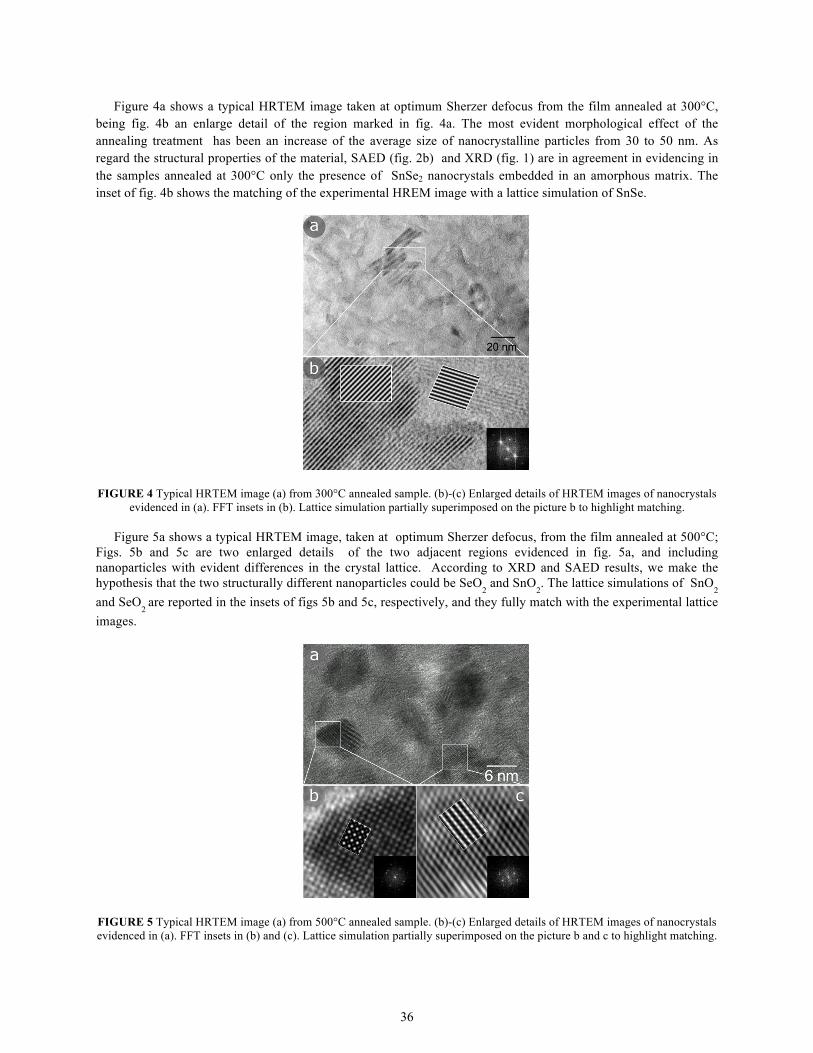
Figure 4a shows a typical HRTEM image taken at optimum Sherzer defocus from the film annealed at 300°C, being fig. 4b an enlarge detail of the region marked in fig. 4a. The most evident morphological effect of the annealing treatment has been an increase of the average size of nanocrystalline particles from 30 to 50 nm. As regard the structural properties of the material, SAED (fig. 2b) and XRD (fig. 1) are in agreement in evidencing in the samples annealed at 300°C only the presence of SnSe2 nanocrystals embedded in an amorphous matrix. The inset of fig. 4b shows the matching of the experimental HREM image with a lattice simulation of SnSe.
FIGURE 4 Typical HRTEM image (a) from 300°C annealed sample. (b)-(c) Enlarged details of HRTEM images of nanocrystals evidenced in (a). FFT insets in (b). Lattice simulation partially superimposed on the picture b to highlight matching.
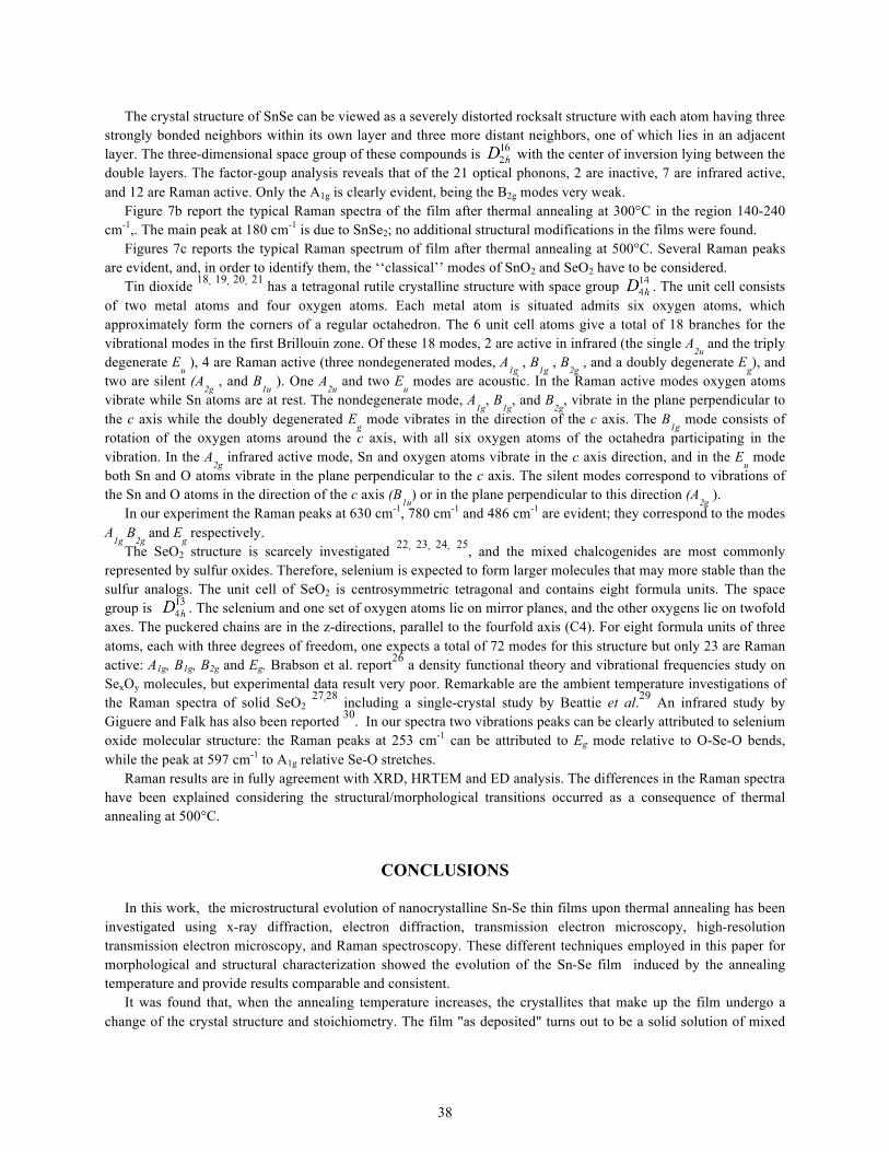
Figure 5a shows a typical HRTEM image, taken at optimum Sherzer defocus, from the film annealed at 500°C;
Figs. 5b and 5c are two enlarged details of the two adjacent regions evidenced in fig. 5a, and including nanoparticles with evident differences in the crystal lattice. According to XRD and SAED results, we make the hypothesis that the two structurally different nanoparticles could be SeO
2 and SnO
2. The lattice simulations of SnO
2 and SeO
2 are reported in the insets of figs 5b and 5c, respectively, and they fully match with the experimental lattice
images.
FIGURE 5 Typical HRTEM image (a) from 500°C annealed sample. (b)-(c) Enlarged details of HRTEM images of nanocrystals evidenced in (a). FFT insets in (b) and (c). Lattice simulation partially superimposed on the picture b and c to highlight matching.
36

The reported results indicate that annealing treatment at 500°C is capable to cause a complete structural and morphologic modification of the material under investigation. First of all, the material endures one structural transition from SnSe to a mixture of SeO
2 and SnO
2; in addition, the average size of nanocrystalline particles
decreases until 10 nm. As conclusion, thermal annealed films are a solid solution of tin oxide and selenium oxide.
Raman Spectroscopy
Figure 6 shows the Raman spectra of the as-deposited film and annealed films, 300 and 500°C. The as deposited films and the films annealed at 300 °C) show evident Raman peaks in the low-frequency region (below 200 cm-1), while for samples annealed at 500 temperatures, the Raman spectra show contributions also in the higher frequency region, where the ‘classical’ modes of SnO2 and SeO2 should be seen.
FIGURE 6 Raman spectra of Selenium-Tin mixed oxide thin films of as-deposited sample, annealed sample at 300° and
annealed sample at 500°. Note that the spectra have been shifted in order to ensure better visualization. Figure 7a shows the Raman spectrum of as deposited thin film in the region 140-240 cm-1. Two raman peaks are
clearly observed at 150 and 180 cm-1. Their presence was confirmed by repeated measurements with different laser power. These peaks are assigned by examining the polarization properties of scattered light. It was found that the 150 cm-1 and 180 cm-1 peaks correspond to the A1g mode of SnSe and SnSe2, respectively 16, 17.
In the structure of SnSe2, the metal atom (Sn) is octahedrally coordinated to the chalcogen atom (Se), and these form essentially two-dimensional layers with the metal atoms sandwiched between two layers of chalcogen atoms. The nanograins of SnSe2 structure has space group . There are nine vibrational modes; three E modes in which the atomic motions are parallel to the basal plane, are doubly degenerate; and three A modes in which the atomic motions are perpendicular to the layer are non-degenerates modes. The acoustic modes are A2u and Eu, so that there are four optic modes, two Raman actives modes A1g and Eg and two IR active modes A2u and Eu. Therefore, only the A1g mode is able to give very strong lines in the Raman spectrum.
FIGURE 7 Raman spectra details on as deposited (picture a) film, 300°C annealed (picture b) and 500°C annealed (picture c).
37
The crystal structure of SnSe can be viewed as a severely distorted rocksalt structure with each atom having three strongly bonded neighbors within its own layer and three more distant neighbors, one of which lies in an adjacent layer. The three-dimensional space group of these compounds is with the center of inversion lying between the double layers. The factor-goup analysis reveals that of the 21 optical phonons, 2 are inactive, 7 are infrared active, and 12 are Raman active. Only the A1g is clearly evident, being the B2g modes very weak.
Figure 7b report the typical Raman spectra of the film after thermal annealing at 300°C in the region 140-240 cm-1,. The main peak at 180 cm-1 is due to SnSe2; no additional structural modifications in the films were found.
Figures 7c reports the typical Raman spectrum of film after thermal annealing at 500°C. Several Raman peaks are evident, and, in order to identify them, the ‘‘classical’’ modes of SnO2 and SeO2 have to be considered.
Tin dioxide 18, 19, 20, 21 has a tetragonal rutile crystalline structure with space group . The unit cell consists of two metal atoms and four oxygen atoms. Each metal atom is situated admits six oxygen atoms, which approximately form the corners of a regular octahedron. The 6 unit cell atoms give a total of 18 branches for the vibrational modes in the first Brillouin zone. Of these 18 modes, 2 are active in infrared (the single A
2u and the triply
degenerate Eu ), 4 are Raman active (three nondegenerated modes, A
1g , B
1g , B
2g , and a doubly degenerate E
g), and
two are silent (A2g
, and B1u
). One A2u
and two Eu modes are acoustic. In the Raman active modes oxygen atoms
vibrate while Sn atoms are at rest. The nondegenerate mode, A1g
, B1g
, and B2g
, vibrate in the plane perpendicular to the c axis while the doubly degenerated E
g mode vibrates in the direction of the c axis. The B
1g mode consists of
rotation of the oxygen atoms around the c axis, with all six oxygen atoms of the octahedra participating in the vibration. In the A
2g infrared active mode, Sn and oxygen atoms vibrate in the c axis direction, and in the E
u mode
both Sn and O atoms vibrate in the plane perpendicular to the c axis. The silent modes correspond to vibrations of the Sn and O atoms in the direction of the c axis (B
1u) or in the plane perpendicular to this direction (A
2g ).
In our experiment the Raman peaks at 630 cm-1, 780 cm-1 and 486 cm-1 are evident; they correspond to the modes A1g
B2g
and Eg respectively.
The SeO2 structure is scarcely investigated 22, 23, 24, 25, and the mixed chalcogenides are most commonly represented by sulfur oxides. Therefore, selenium is expected to form larger molecules that may more stable than the sulfur analogs. The unit cell of SeO2 is centrosymmetric tetragonal and contains eight formula units. The space group is . The selenium and one set of oxygen atoms lie on mirror planes, and the other oxygens lie on twofold axes. The puckered chains are in the z-directions, parallel to the fourfold axis (C4). For eight formula units of three atoms, each with three degrees of freedom, one expects a total of 72 modes for this structure but only 23 are Raman active: A1g, B1g, B2g and Eg. Brabson et al. report26 a density functional theory and vibrational frequencies study on SexOy molecules, but experimental data result very poor. Remarkable are the ambient temperature investigations of the Raman spectra of solid SeO2
27,28 including a single-crystal study by Beattie et al.29 An infrared study by Giguere and Falk has also been reported 30. In our spectra two vibrations peaks can be clearly attributed to selenium oxide molecular structure: the Raman peaks at 253 cm-1 can be attributed to Eg mode relative to O-Se-O bends, while the peak at 597 cm-1 to A1g relative Se-O stretches.
Raman results are in fully agreement with XRD, HRTEM and ED analysis. The differences in the Raman spectra have been explained considering the structural/morphological transitions occurred as a consequence of thermal annealing at 500°C.
CONCLUSIONS
In this work, the microstructural evolution of nanocrystalline Sn-Se thin films upon thermal annealing has been investigated using x-ray diffraction, electron diffraction, transmission electron microscopy, high-resolution transmission electron microscopy, and Raman spectroscopy. These different techniques employed in this paper for morphological and structural characterization showed the evolution of the Sn-Se film induced by the annealing temperature and provide results comparable and consistent.
It was found that, when the annealing temperature increases, the crystallites that make up the film undergo a change of the crystal structure and stoichiometry. The film "as deposited" turns out to be a solid solution of mixed
38

nanocrystals SnSe and SnSe2. After a heat treatment at 300°C is obtained a nanostructured film of SnSe2 stoichiometrically pure. After thermal annealing at higher temperatures, the films begin to oxidize. At 500 ° C the obtained film appears to be a solid and homogeneous solution of SnO2 and SeO2 nanocrystals.
ACKNOWLEDGEMENTS
This work was is a part of a project included in the PON 254/Ric. (Strengthening of "RESEARCH CENTRE FOR THE HUMAN AND ENVIRONMENT HEALTH " Code PONa3_00334)
1 M.L. Terranova, S. Orlanducci, A. Serra, D. Manno, E. Filippo, M. Rossi, Chemical Physics Letters, 509 (2011) 152-157 2 E. Filippo, D. Manno, A. Buccolieri, A. Serra, Sensors and Actuators B, 178 (2013) 1-9 3 M. C. Orilall, U. Wiesner, Chem Soc Rev, 40 (2011) 520-535 4 I. Tanahashi, T. Tohda, J Am Ceram Soc, 791 (1996) 796-798 5 D.Y. Shang, H. Matsuno, Y. Saito, S. Suganomato, J Appl Phys, 80 (1996) 406-408 6 D. Brusilovskyl, M. Eyal, R. Reisfeld, Chem Phys Lett, 153 (1988) 203-209 7 J.H. Fendler, Chem. Mater, 8 (1996) 1616-1624 8 Y. Xia, J. A. Rogers, K.E. Paul, G.M. Whitesides, Chem Rev 99 (1999) 1823-1848 9 N.R. Mathews, Solar Energy 86 (2012) 1010-1016 10 E. Comini, Analytica, Chimica Acta, 568 (2006) 28-40 11 L. Vayssieres, Comptes Rendus Chimie 9 (2006) 691-701 12 D. Manno, G. Micocci, A. Serra, A. Tepore, J of Appl Phys 83 (1998) 3541-3546 13 L. Vayssieres, A. Hagfeldt, S.E. Lindquist, Pure Appl Chem, 72 (2000) 47-52 14 D. Manno, M. Di Giulio, T. Siciliano, E. Filippo, A. Serra, J of Phys D: Appl Phys, 34 (2001) 2097-2102 15 D. Manno, M. Di Giulio, G. Micocci, A. Serra, A. Tepore, J of Appl Phys, 88 (2000) 6571-6577 16 H.R. Chandrasekhar, R.G. Humpreys, U. Zwick, M. Cardona, Phys Rev B, 15 (1977) 2177-2183 17 A.J. Smith, P.E. Meek, W. Y. Liang, J Phys C: Solid State Phys, 10 (1977) 1321-1333 18 P.S. Peercy, B. Morosin, Phys Rev B, 7 (1973) 2779-2786 19 K.N. Yu, Y. Xiong, Y. Liu, C. Xiong, Phys Rev B, 55 (1997) 2666-2671 20 T. Sato, T. Asari, J Phys Soc of Japan, 64 (1995) 1193-1199 21 A. Dieguez, A. Romano-Rodrıguez, A. Vila`, J. R. Morante, J Appl Phys, 90 (2001) 1550-1556 22 H. Takeo, E. Hirota, Y. Morino, J Mol Spectrosc, 34 (1970) 370-382 23 A. Anderson, A. Sanders, W. Smith, J Raman Spectrosc, 31 (2000) 403-406 24 K.J. Palmer, N. Elliott, J Am Chem Soc, 60 (1938) 1309-1310 25 E.Z. Zasorin, I.M. Zharskii, G.F. Pinaev, V.N. Kupreev, V.P. Spiridonov, Russ J Struct Chem, 15 (1974) 588-590 26 C.D. Brabson, L. Andrews, C.J. Marsden, J Phys Chem, 100 (1996) 16487–16494 27 H. Gerding, Rec Trav Chim 60 (1941) 728-731 28 A. Simon, R. Paetzold, Naturwiss, 44 (1957) 108-108 29 I.R. Beattie, N. Cheatham, T.R. Gilson, K.M.S. Livingston, D.J. Reynolds, J Chem Soc (A) (1971) 1910-1917 30 P.A. Giguere, M. Falk, Spectrochim Acta, 16 (1960) 1-5
39