solid state luminescent radiation imaging detectors...
TRANSCRIPT

Rosa Maria MonterealiENEA, C.R. Frascati, Technical Unit for the Development and Applications of Radiations,
Photonics Micro- and Nano-structures Lab., Via E. Fermi 45, 00044 Frascati (Rome) Italy
http://www.frascati.enea.it/UTAPRAD/lab_mnf.htm, http://www.enea.it/it/Ricerca_sviluppo/nuove-tecnologie
1
Solid state luminescent radiation imaging detectors
based on LiF crystals and thin films
2 mmProton beam image on a LiF film
E = 3 MeV
Soft X-ray radiography of a dragonfly wing on a LiF film
E = 300 – 800 eV
F. Bonfigli
S. Libera
M. Piccinini
M.A.Vincenti
ENEA C.R.
Frascati
E. Nichelatti
ENEA C.R.
Casaccia
Phd of Industrial Engineering
Research activities on Advanced Materials
8 Giugno 2015, Universita’ di Tor Vergata

ENEA Italian National Agency for New Technologies,
Energy and Sustainable Economic Development
2
Main activities
•Research and experimentation on controlled nuclear
fusion, both magnetically confined and inertial;
•Development of specific technologies based on this
research, including superconductivity, neutron-matter
interaction, materials and automated maintenance;
•Research and development of laser sources (gas,
solid-state, free-electron) and of laser applications in
environmental, industrial and medical diagnostics,
nano and micro systems, metrology and laser vision;
•Research and development of electron and proton
accelerators for scientific, medical and industrial
applications;
•Studies and research for environmental protection and
territorial planning.
ENEA conducts scientific research and
technology development activities that draw on a
wide range of expertise, advanced facilities and
tools located at its own Research Centres,
operating in support of ENEA's programmes and
the Nation's productive system.

Photonics, nanotechnologies & nanophotonics
3
Photonics
is the science of the harnessing of light. Photonics encompasses the generation of light, the
detection of light, the management of light through guidance, manipulation, and amplification,
and most importantly, its utilisation for the benefit of mankind (Pierre Aigrain, 1967)
Nanotechnologies
technologies for realization and characterization of functionalized materials and devices with
enhanced properties based on the control of matter on a nanometric scale.
They include the ability to observe, measure and manipulate matter on an atomic and molecular
scale. In a simplified approach, “nano-products” are materials and/or devices with at least one
functional component sized less than 100 nm, but their relevance is related to nano-effects,
which lead to extraordinary enhancements in material properties.
Nanophotonics
science & engineering of light-matter interaction on a spatial scale comparable and/or less
than the wavelength of the e.m radiation, 300 nm at optical (UV-VIS-NIR) wavelenghts.
An International
Year of Light
and Light-based Technologies
2015
Luce ENEA C.R. Frascati
Imaging 15-16 ottobre, 2015
Microscopia:
Spettri di opportunita’
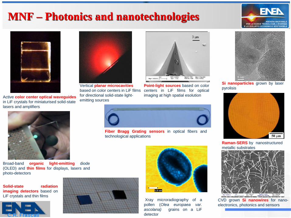
Point-light sources based on color
centers in LiF films for optical
imaging at high spatial esolution
Vertical planar microcavities
based on color centers in LiF films
for directional solid-state light-
emitting sourcesActive color center optical waveguides
in LiF crystals for miniaturised solid-state
lasers and amplifiers
Solid-state radiation
imaging detectors based on
LiF crystals and thin films
Broad-band organic light-emitting diode
(OLED) and thin films for displays, lasers and
photo-detectors
Xray microradiography of a
pollen (Olea europaea var.
ascolana) grains on a LiF
detector
CVD grown Si nanowires for nano-
electronics, photonics and sensors
Fiber Bragg Grating sensors in optical fibers and
technological applications
Si nanoparticles grown by laser
pyrolisis
Raman-SERS by nanostructured
metallic substrates
MNF – Photonics and nanotechnologies
Introduction and objectives
5
Since ancient times, X-ray and ion beams of different energies have been widely
investigated for many applications, including radiation diagnostics, radiobiology and
radiotherapy as far as medical applications are concerning.
Luminescent phenomena are successfully used in solid-state radiation detectors and
dosimeters based on point defects in insulating materials.
In the last decade, LiF crystals and polycrystalline thin films have been successfully tested
as novel solid-state detectors for X-ray imaging at nanoscale, based on the optical reading
of the photoluminescence (PL) of radiation-induced point defects emitting in the visible
spectral range.
On the other hand, doped (Mg, Ti, P) LiF materials are widely used in dosimetry
exploiting thermoluminescence (TL).
Very recently solid state LiF film radiation detectors, exploiting the PL of broad-band
light-emitting radiation-induced stable color centers (CCs), have been proposed and tested
for imaging and characterization of proton beams produced by a linear accelerator for
protontheraphy under development at ENEA C.R. Frascati, with the challenging aim of
investigate radiation dosimeters based on PL of CCs in this promising material.
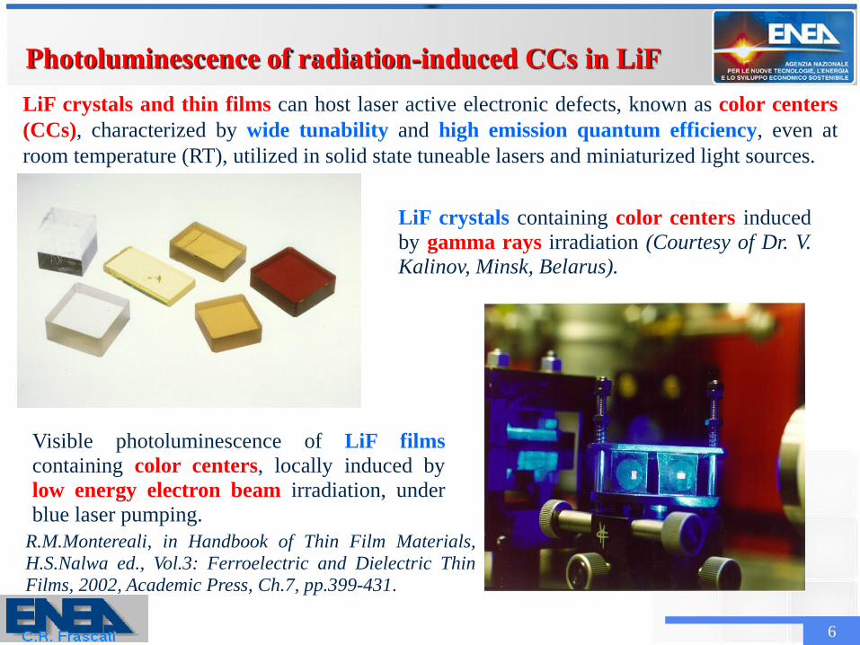
Photoluminescence of radiation-induced CCs in LiF
6
LiF crystals and thin films can host laser active electronic defects, known as color centers
(CCs), characterized by wide tunability and high emission quantum efficiency, even at
room temperature (RT), utilized in solid state tuneable lasers and miniaturized light sources.
LiF crystals containing color centers induced
by gamma rays irradiation (Courtesy of Dr. V.
Kalinov, Minsk, Belarus).
Visible photoluminescence of LiF films
containing color centers, locally induced by
low energy electron beam irradiation, under
blue laser pumping.
R.M.Montereali, in Handbook of Thin Film Materials,
H.S.Nalwa ed., Vol.3: Ferroelectric and Dielectric Thin
Films, 2002, Academic Press, Ch.7, pp.399-431.
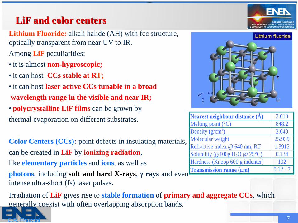
LiF and color centers
7
Nearest neighbour distance (Å) 2.013
Melting point (°C) 848.2
Density (g/cm3) 2.640
Molecular weight 25.939
Refractive index @ 640 nm, RT 1.3912
Solubility (g/100g H2O @ 25°C) 0.134
Hardness (Knoop 600 g indenter) 102
Transmission range (m) 0.12 - 7
Lithium Fluoride: alkali halide (AH) with fcc structure,
optically transparent from near UV to IR.
Among LiF peculiarities:
•it is almost non-hygroscopic;
• it can host CCs stable at RT;
•it can host laser active CCs tunable in a broad
wavelength range in the visible and near IR;
•polycrystalline LiF films can be grown by
thermal evaporation on different substrates.
Color Centers (CCs): point defects in insulating materials,
can be created in LiF by ionizing radiation,
like elementary particles and ions, as well as
photons, including soft and hard X-rays, rays and even
intense ultra-short (fs) laser pulses.
Irradiation of LiF gives rise to stable formation of primary and aggregate CCs, which
generally coexist with often overlapping absorption bands.

Optical properties of color centers in LiF
8
0.0
0.2
0.4
0.6
0.8
1.0
F2
-F
3
-F
3
+F
2
F2
-F
3
-
F3
+F
2
Absor
ption
400 600 800 1000 1200 14000.0
0.2
0.4
0.6
0.8
1.0
F2
+
F2
+
Wavelength (nm)
Emiss
ion
F2 and F3+ centers are laser active F-aggregate defects, consisting in two
electrons bound to two and three close anion vacancies, respectively.
F center is an anion vacancy occupied by
an electron; it is not active centers in LiF.
F2 ~ 18 ns; W32, W10 >> 1/
E3-E0 = 2.79 eV; E2-E1 = 1.83 eV
GS,
E0
URES, E3
W10
W32
1/
RES, E2
URGS, E1

Thermally evaporated polycrystalline LiF films
9
(a) (b)
(c) (d)
Ts
t
(a) (b)
(c) (d)
(a) t 1 m, Ts=30°C (b) t 1 m, Ts=300°C
(c) t 1.75 m, Ts=30°C (d) t 1.75 m, Ts=300°C on glass substrates.
oscillating quartzsubstrate
holder
crucible
Deposition parameters:
Pressure < 10-6 mbar
Evaporation rate
R = 0.5-2 nm/s
Film thickness t
up to 2 m
Substrate temperature
Ts=30-350°C
Nature of the substrateG.Baldacchini, M.Cremona, G.d'Auria, S.Martelli, R.M.Montereali,
M.Montecchi, E.Burattini, A.Grilli, A.Raco, NIM B 116(1996)447-451
LiF films of different thicknesses t grown at different substrate temperature Ts
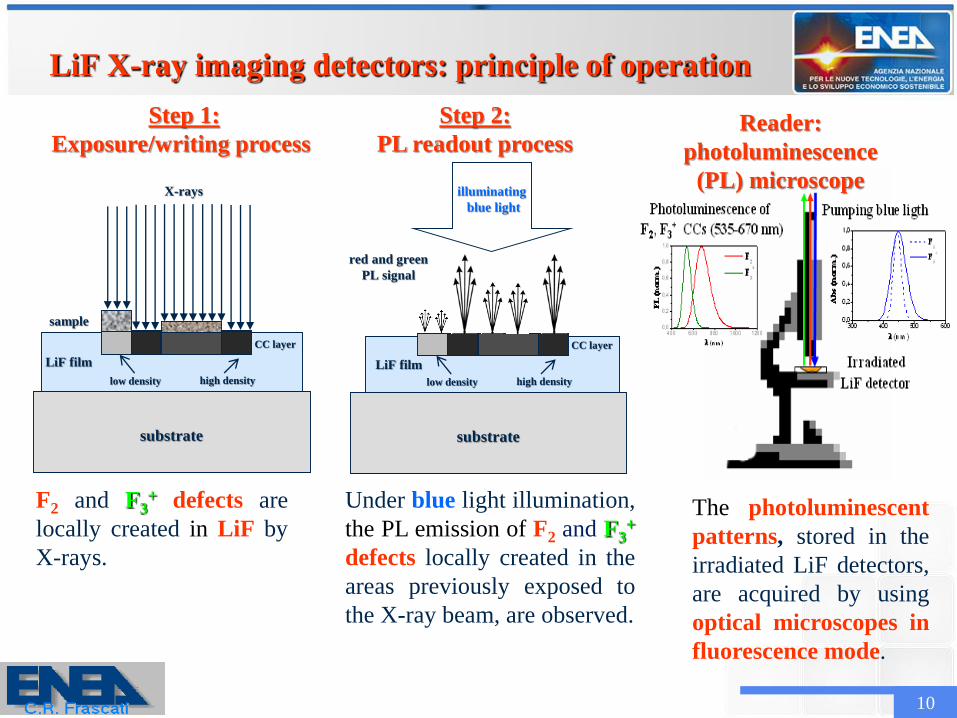
LiF X-ray imaging detectors: principle of operation
10
substrate
LiF film
sample
CC layer
high densitylow density
X-rays
red and green
PL signal
substrate
LiF film
CC layer
high densitylow density
illuminating
blue light
Step 1:
Exposure/writing process
Step 2:
PL readout processReader:
photoluminescence
(PL) microscope
F2 and F3+ defects are
locally created in LiF by
X-rays.
Under blue light illumination,
the PL emission of F2 and F3+
defects locally created in the
areas previously exposed to
the X-ray beam, are observed.
The photoluminescent
patterns, stored in the
irradiated LiF detectors,
are acquired by using
optical microscopes in
fluorescence mode.

LiF radiation imaging detectors:
high spatial resolution on a wide field of view
11
2 mm 1) Conventional wide field fluorescence microscope
Soft X-ray micro-radiography of a dragonfly (Pyrrhesoma
nymphula) wing on a LiF film.
Near-field fluorescence optical microscope (SNOM)
30 x 40 um2 SNOM image of a mosquito wing micro-
radiograph stored in a LiF film
2) Confocal laser
fluorescence
microscope (CLSM)
Micro-radiography of a
mosquito (Diptera)
wing on a LiF film
50 nm spatial
resolution
250 nm
spatial
resolution
G.Baldacchini, F.Bonfigli, A.Faenov, F.Flora, R.M.Montereali, A.Pace,
T.Pikuz, L.Reale, J. Nanoscience and Nanotechnology 3,6(2003)483
A.Ustione, A.Cricenti, F.Bonfigli, F.Flora,
A.Lai, T.Marolo, R.M. Montereali, G.
Baldacchini, A. Faenov, T. Pikuz, L. Reale,
Appl. Phys. Lett. 88 (2006) 141107
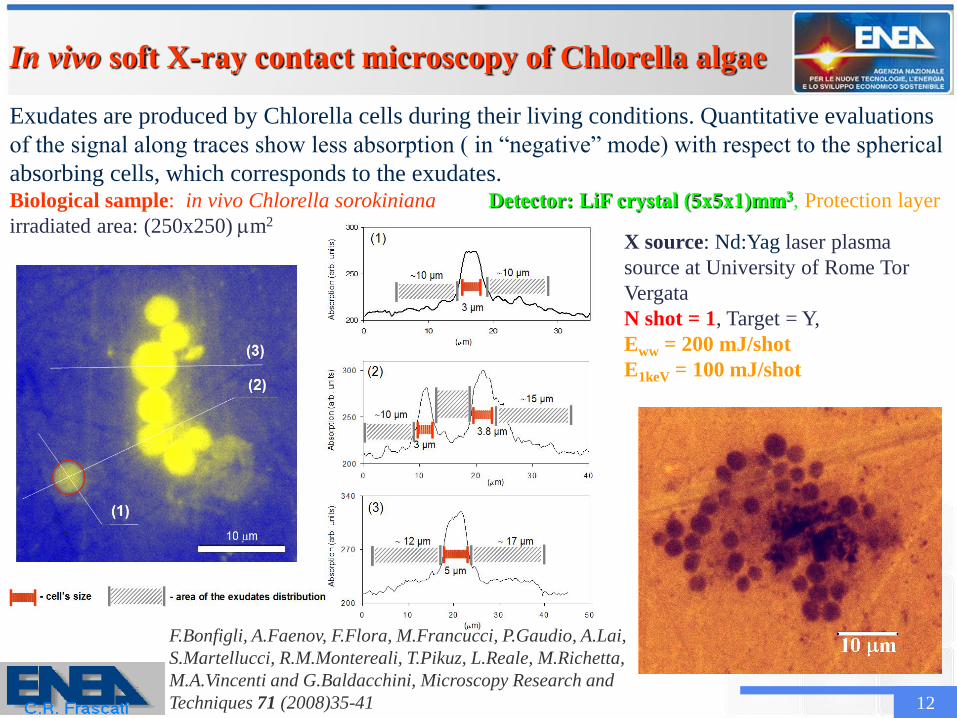
12
F.Bonfigli, A.Faenov, F.Flora, M.Francucci, P.Gaudio, A.Lai,
S.Martellucci, R.M.Montereali, T.Pikuz, L.Reale, M.Richetta,
M.A.Vincenti and G.Baldacchini, Microscopy Research and
Techniques 71 (2008)35-41
Exudates are produced by Chlorella cells during their living conditions. Quantitative evaluations
of the signal along traces show less absorption ( in “negative” mode) with respect to the spherical
absorbing cells, which corresponds to the exudates.Biological sample: in vivo Chlorella sorokiniana Detector: LiF crystal (5x5x1)mm3, Protection layer
irradiated area: (250x250) m2
In vivo soft X-ray contact microscopy of Chlorella algae
X source: Nd:Yag laser plasma
source at University of Rome Tor
Vergata
N shot = 1, Target = Y,
Eww = 200 mJ/shot
E1keV = 100 mJ/shot

Solid-state radiation imaging luminescent LiF detectors
13
Peculiarities
Defect size 0.001 m
Readout: optical reading (PL)
Main characteristics
high spatial resolution ( intrinsic < 2 nm, standard 250 nm )
large field of view ( > 20 cm2, limited only by technologies of LiF film growth process)
efficiency of PL process (high emission quantum efficiencies of F2 and F3+ CCs in LiF)
stable storage of images (stability of CCs at RT in LiF)
Main advantages
•easy handling: no development need and no sensitivity to ambient light
•availability of readout instrumentation (PL excitation and emission in the visible range)G.Baldacchini, et al., Review Scientific Instruments 76(2005)113104-1,12 (Also selected for publication
in the Virtual Journal of Biological Physics Research 10(11), December 1, 2005) & Nanoforum 2011
• versatility: film geometry compatible with protective layers and different substrates
• multi-purpose: radiation sensitivity to X-ray (20 eV-40 keV), but also energetic photons
() and charged particles,
• wide dynamic range ( > 103), dependent on the used radiation, irradiation conditions, film
properties (and fluorescence reader characteristics)
In the last years, at ENEA C.R. Frascati, we propose^, realized and developed*
Novel soft X-ray imaging thin-film detectors based on photoluminescence (PL)
of radiation-induced ligth-emitting color centers in Lithium Fluoride (LiF)
^ENEA patent n. 514, N. TO2002A000575;
*ENEA patent n. 752, N. RM2012A000183

LiF film growth and confocal microscopy at ENEA C.R.
Frascati: Micro- and Nano-structures Laboratory
3 m thick LiF film on (5x5)
mm2 Si substrate produced by
ENEA Solid State Laser Lab
Commercial 0.5 m thick
PMMA film on (5x5) mm2
Si substrate
Nikon Eclipse
80i-C1 equipped
with an Argon
laser at 458 nm.
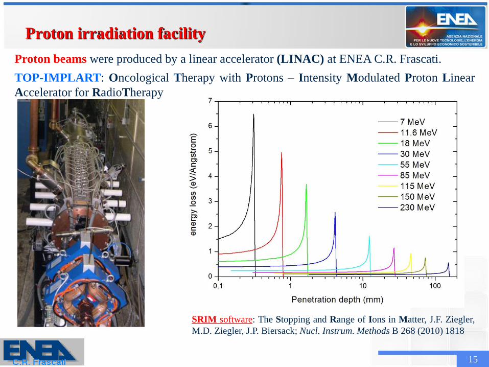
Proton irradiation facility
15
Proton beams were produced by a linear accelerator (LINAC) at ENEA C.R. Frascati.
TOP-IMPLART: Oncological Therapy with Protons – Intensity Modulated Proton Linear
Accelerator for RadioTherapy
SRIM software: The Stopping and Range of Ions in Matter, J.F. Ziegler,
M.D. Ziegler, J.P. Biersack; Nucl. Instrum. Methods B 268 (2010) 1818

2D LiF film radiation detectors for proton imaging
16
3 MeV proton beam image
on LiF film
Fluorescence Microscope: Nikon Eclipse 80-i,
s-CMOS camera: Andor NEO
Step 1:
Exposure of LiF sample to proton beams
Proton Beam parameters
•Energy: 3 MeV and 7 MeV (pulsed source @ 50 Hz)
•Actual Energy after 50 m thick kapton window:
2.23 MeV and 6.65 MeV
•Pulse duration: 60 ms Charge/pulse: 58 pC
•Beam diameter: ~ 3 mm
•Fluence range: 1011 – 1015 protons/cm2
•Proton implantation depth in LiF @ 2.23 MeV: 45 m
•Proton implantation depth in LiF @ 6.65 MeV: 295 m
M. Piccinini, F. Ambrosini, A. Ampollini, M.
Carpanese, L. Picardi, C. Ronsivalle, F. Bonfigli,
S. Libera, M.A. Vincenti and R.M. Montereali,
J. Lum. 156 (2014) 170-174
• Polished LiF crystals: 10x10 mm2, 1 mm thick
• Polycrystalline LiF films thermally evaporated
on glass substrates, 1 m thick
Step 2:
PL optical readout of CCs PL signal by
a conventional fluorescence microscope

Conclusions
17
•Novel two-dimensional (2D) LiF thin-film imaging detectors, sensitive to soft and hard X-
rays, utilising atomic-scale point defects as minimum luminescent units, are under
development.
•Soft X-ray micro-radiography and microscopy images have been already obtained with
sub-micrometric spatial resolution in LiF, even for in vivo cells.
•Solid-state LiF film luminescent radiation imaging detectors were successfully tested also
for hard X-rays from conventional X-ray tubes.
•The use of polycrystalline LiF thin films allows sub-micron spatial resolution even at
highest X-ray energies, suitable for radiation diagnostics.
•Accurate accumulated 2D dose distribution with high spatial resolution over large areas
were successfully demonstrated for the first time by using low energy proton beams.
• A wide dynamic range, covering three orders of magnitude of doses, together with non
destructive optical PL readout in a conventional optical microscope, was obtained in LiF thin-
films.
•Tissue equivalence of LiF materials makes their use attractive in radiation detectors based
on PL of CCs for clinical dosimetry, including hadrontheraphy, but
radiation sensitivity should be increased to measure low doses with great accuracy
Nanophotonics (control of light-matter interactions on a sub-micrometric scale)
& nanotechnologies (control of electronic defects at nanoscale)
Acknowledgements
18
Luce
Imaging
Microscopia:
Spettri di
Applicazione
ENEA
C.R. Frascati
15-16 ottobre,
2015
Acknowledgements
19
ENEA C.R. Frascati
UTAPRAD-SOR
F. Ambrosini,
A. Ampollini,
M. Carpanese,
L. Picardi,
C. Ronsivalle
S. Bollanti
P. Di Lazzaro
F. Flora
L. Mezi
D. Murra
UTAPRAD-DIM
Dr.ssa A. Lai
Dr. S. Almaviva
UTFUS
Dr. A. Rufoloni
Dip. Fisica Universita’Roma Tor Vergata
Dr. P. Del Gaudio
Prof. S. Martellucci
Dr.ssa M. Richetta
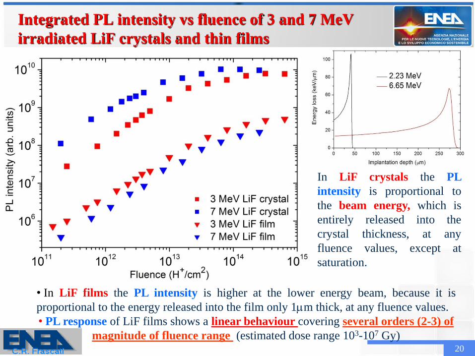
Integrated PL intensity vs fluence of 3 and 7 MeV
irradiated LiF crystals and thin films
20
• In LiF films the PL intensity is higher at the lower energy beam, because it is
proportional to the energy released into the film only 1m thick, at any fluence values.
• PL response of LiF films shows a linear behaviour covering several orders (2-3) of
magnitude of fluence range (estimated dose range 103-107 Gy)
In LiF crystals the PL
intensity is proportional to
the beam energy, which is
entirely released into the
crystal thickness, at any
fluence values, except at
saturation.
Increased collection efficiency: optical modelling
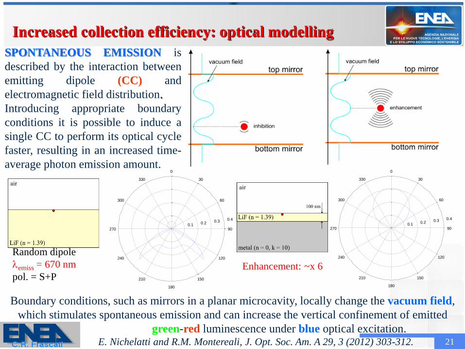
21
SPONTANEOUS EMISSION is
described by the interaction between
emitting dipole (CC) and
electromagnetic field distribution.
Introducing appropriate boundary
conditions it is possible to induce a
single CC to perform its optical cycle
faster, resulting in an increased time-
average photon emission amount.
Boundary conditions, such as mirrors in a planar microcavity, locally change the vacuum field,
which stimulates spontaneous emission and can increase the vertical confinement of emitted
green-red luminescence under blue optical excitation.E. Nichelatti and R.M. Montereali, J. Opt. Soc. Am. A 29, 3 (2012) 303-312.
0.1 0.2 0.3 0.4
30
210
60
240
90270
120
300
150
330
180
0
0.1 0.2 0.3 0.4
30
210
60
240
90270
120
300
150
330
180
0
Random dipole
emiss = 670 nm
pol. = S+PEnhancement: ~x 6
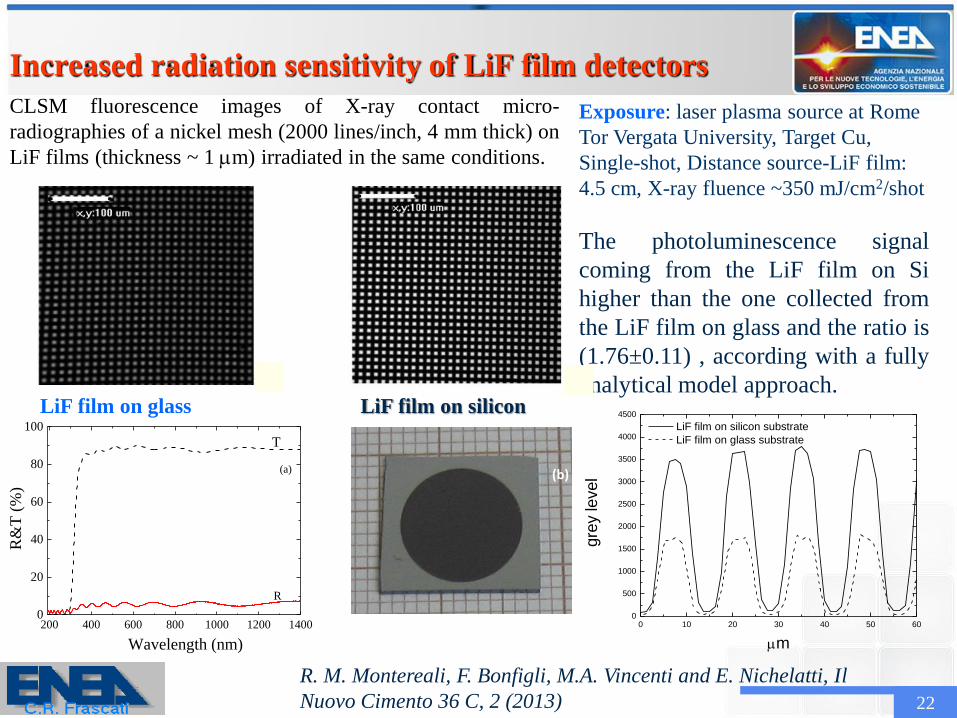
Exposure: laser plasma source at Rome
Tor Vergata University, Target Cu,
Single-shot, Distance source-LiF film:
4.5 cm, X-ray fluence ~350 mJ/cm2/shot
The photoluminescence signal
coming from the LiF film on Si
higher than the one collected from
the LiF film on glass and the ratio is
(1.76±0.11) , according with a fully
analytical model approach.
Increased radiation sensitivity of LiF film detectors
22
0 10 20 30 40 50 600
500
1000
1500
2000
2500
3000
3500
4000
4500
LiF film on silicon substrate
LiF film on glass substrate
gre
y le
vel
m
LiF film on glass LiF film on silicon
R. M. Montereali, F. Bonfigli, M.A. Vincenti and E. Nichelatti, Il
Nuovo Cimento 36 C, 2 (2013)
(b)
200 400 600 800 1000 1200 14000
20
40
60
80
100
R&
T (
%)
Wavelength (nm)
T
R
(a)
CLSM fluorescence images of X-ray contact micro-
radiographies of a nickel mesh (2000 lines/inch, 4 mm thick) on
LiF films (thickness ~ 1 m) irradiated in the same conditions.

Controlled manipulation of single atoms at AH surface
23
Ever since the 1990s, physicists have been able to directly control surface structures by
moving and positioning single atoms to certain atomic sites. A number of atomic
manipulations have previously been demonstrated both on conducting or semi-conducting
surfaces, mainly under very low temperatures. However, the fabrication of artificial
structures on an insulator at RT is still a long-standing challenge and previous attempts
were uncontrollable and did not deliver the desired results.
Using the tip of an atomic force microscope,
single bromine atoms were placed on a
sodium chloride (NaCl) surface to construct
the shape of the “Swiss cross”. The tiny cross
is made of 20 bromine atoms and was
created by exchanging chlorine with bromine
atoms. It measures only 5.6 nanometers
square and represents the largest number of
atomic manipulations ever achieved at RT.
It represents an important step towards the
fabrication of a new generation of
electromechanical systems, advanced
atomic-scale data storage devices and logic
circuits (S. Kawai et al, Nature
Commun.(2014)1-7)Source: http://www.unibas.ch/
Thank for your attention
24
Luce
Imaging
Microscopia:
Spettri di
opportunita’
ENEA
C.R. Frascati
8-9 ottobre,
2015

LiF film based radiation detectors : enhanced sensitivity
25
Crystal
The photoluminescence signal coming from the LiF film on Si is
significantly larger (8±2) than the one coming from the LiF
crystal:
light confinement effects in the investigated planar
microstructures (photonics)
polycrystalline films: high surface to volume ratio modifies
the CCs formation and stabilization processes (surface effects)
(R.M.Montereali, S.Almaviva, F.Bonfigli, A.Faenov, F.Flora, I.Franzini,
E.Nichelatti, T. Pikuz, M.A.Vincenti, G.Baldacchini, Proc. SPIE Vol.
6593, 2007).
LiF crystalAFM image of the surface of a LiF
film 3.3 m thick thermally
evaporated on a glass substrate at Ts
= 280°C.LiF film on Si
The reflective properties
of Si help to recover a
relevant part of lost PL.

Radiation diagnostics: soft X-ray scientific imaging
26
X-ray imaging at the nano- and micro-scale is of great interest, also for biological samples.
Optical Microscopy (OM)
Abbe diffraction limited, ~300 nm for visible light;
novel super-resolution fluorescence technique to
detect the marked fluorescent molecules.
Electronic Microscopy (SEM e TEM)
Limited by preliminary treatments of
sample (dehydration, fixing and dying
with electron dense substances).
Soft X-Ray Microscopy
( : 10 - 0.1 nm , E: 200 eV – 5 keV)
internal structure of samples at a high spatial resolution and
avoiding all specimen preparation
(biological samples also in their normal living state).
The short wavelength gives the potential for high-resolution
imaging.X-ray
microscope
image of the
labelled
microtubule
network in a
whole, hydrated
mammary
epithelial cell.
Photo courtesy
of C. Larabell
X-ray
radiography of
the hand of
Röntgen’s wife
(1896)
Micro-radiography of a dragonfly (Pyrrhesoma
nymphula) wing
27
2 mm
Plasma
10 cm L i F f i l m
X e C l L a s e r :
1 J - 1 0 n s
C u t a p e
t a r g e t
b i o l o g i c a l s a m p l e
X - r a y s
C o l o r
c e n t e r s
g e n e r a t i o n
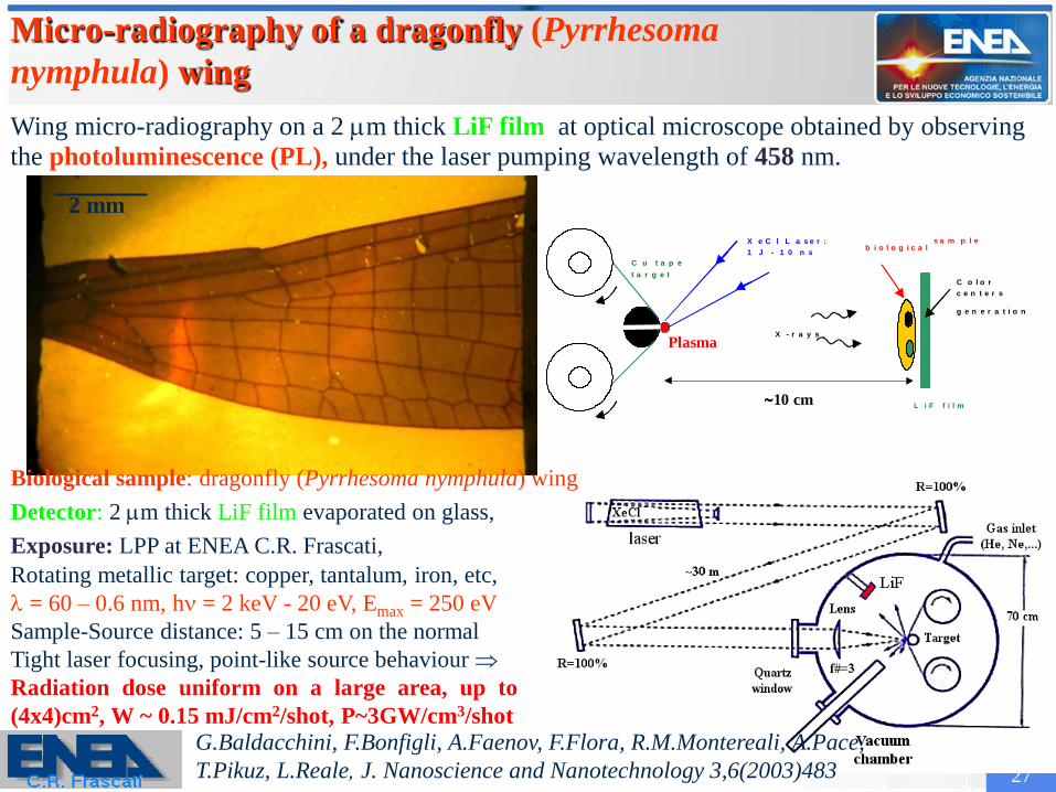
Biological sample: dragonfly (Pyrrhesoma nymphula) wing
Detector: 2 m thick LiF film evaporated on glass,
Exposure: LPP at ENEA C.R. Frascati,
Rotating metallic target: copper, tantalum, iron, etc,
= 60 – 0.6 nm, h = 2 keV - 20 eV, Emax = 250 eV
Sample-Source distance: 5 – 15 cm on the normal
Tight laser focusing, point-like source behaviour
Radiation dose uniform on a large area, up to
(4x4)cm2, W ~ 0.15 mJ/cm2/shot, P~3GW/cm3/shot
G.Baldacchini, F.Bonfigli, A.Faenov, F.Flora, R.M.Montereali, A.Pace,
T.Pikuz, L.Reale, J. Nanoscience and Nanotechnology 3,6(2003)483
Wing micro-radiography on a 2 m thick LiF film at optical microscope obtained by observing
the photoluminescence (PL), under the laser pumping wavelength of 458 nm.
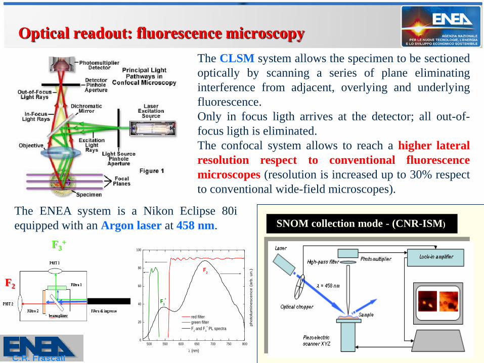
Optical readout: fluorescence microscopy
28
500 550 600 650 700 750 8000
20
40
60
80
100
red filter
green filter
F2 and F
3
+ PL spectra
F3
+
F2
ph
oto
lum
ine
scen
ce
(a
rb. u
n.)
CL
SM
filte
r tr
an
sm
itio
n %
(nm)
The CLSM system allows the specimen to be sectioned
optically by scanning a series of plane eliminating
interference from adjacent, overlying and underlying
fluorescence.
Only in focus ligth arrives at the detector; all out-of-
focus ligth is eliminated.
The confocal system allows to reach a higher lateral
resolution respect to conventional fluorescence
microscopes (resolution is increased up to 30% respect
to conventional wide-field microscopes).
The ENEA system is a Nikon Eclipse 80i
equipped with an Argon laser at 458 nm. SNOM collection mode - (CNR-ISM)
F2
F3+
29
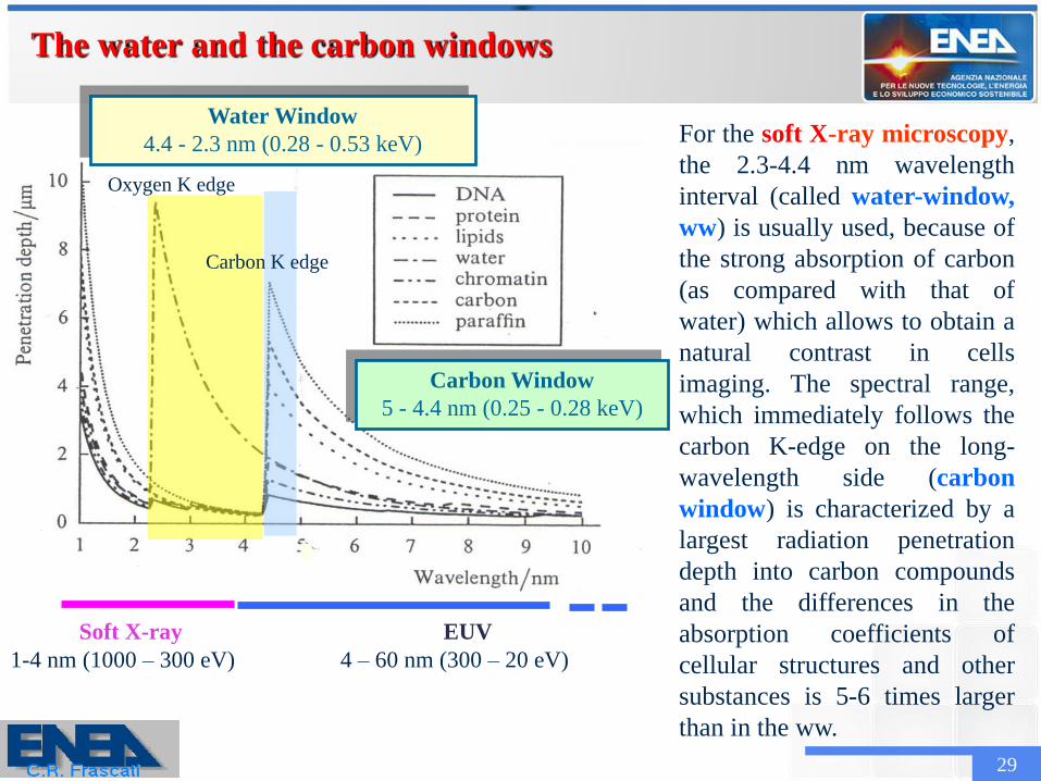
Water Window
4.4 - 2.3 nm (0.28 - 0.53 keV)
Carbon Window
5 - 4.4 nm (0.25 - 0.28 keV)
Oxygen K edge
Soft X-ray
1-4 nm (1000 – 300 eV)
EUV
4 – 60 nm (300 – 20 eV)
Carbon K edge
For the soft X-ray microscopy,
the 2.3-4.4 nm wavelength
interval (called water-window,
ww) is usually used, because of
the strong absorption of carbon
(as compared with that of
water) which allows to obtain a
natural contrast in cells
imaging. The spectral range,
which immediately follows the
carbon K-edge on the long-
wavelength side (carbon
window) is characterized by a
largest radiation penetration
depth into carbon compounds
and the differences in the
absorption coefficients of
cellular structures and other
substances is 5-6 times larger
than in the ww.
The water and the carbon windows
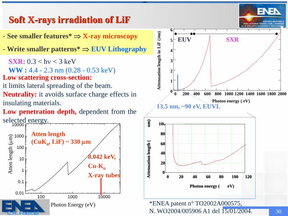
Soft X-rays irradiation of LiF
30
*ENEA patent n° TO2002A000575,
N. WO2004/005906 A1 del 15/01/2004.
0 200 400 600 800 1000 1200 1400 1600 1800 20000
1
2
3
4
5
6
Photon energy ( eV)
Att
enu
ati
on
len
gth
in
LiF
(m
)
EUV SXR
SXR: 0.3 < h < 3 keV
WW : 4.4 - 2.3 nm (0.28 - 0.53 keV)
- See smaller features* X-ray microscopy
- Write smaller patterns* EUV Lithography
100 1000 100000.01
0.1
1
10
100
1000
10000
Att
en l
ength
(
m)
Photon Energy (eV)
Atten length
(CuKa, LiF) ~ 330 m
8.042 keV,
Cu-K
X-ray tubes
13.5 nm, ~90 eV, EUVL
Low scattering cross-section:
it limits lateral spreading of the beam.
Neutrality: it avoids surface charge effects in
insulating materials.
Low penetration depth, dependent from the
selected energy.
0 20 40 60 80 100 1200
20
40
60
80
100
Photon energy ( eV)
Att
enu
ati
on
len
gth
(n
m)

Luminescent radiation detectors based on doped LiF
31
Thermoluminescence Dosimeter
(TLD) glow curve
Doped LiF pellets, powders, …
TLD100
LiF:Mg:Ti 420-460 nm
GR200 TLDHS
LiF:Mg:Cu:P ~ 380 nm
Luminescent phenomena are successfully used in solid-state radiation detectors and
dosimeters based on point defects in insulating materials. Among them,
thermoluminescence (TL) in doped LiF , an alkali halide, radiation sensitive material.
Comparison with similar detectors for X-ray imaging
32
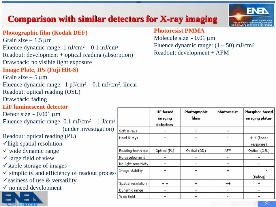
Photographic film (Kodak DEF)
Grain size 1.5 m
Fluence dynamic range: 1 nJ/cm2 – 0.1 mJ/cm2
Readout: development + optical reading (absorption)
Drawback: no visible light exposure
Photoresist PMMA
Molecule size 0.01 m
Fluence dynamic range: (1 – 50) mJ/cm2
Readout: development + AFM
LiF luminescent detector
Defect size 0.001 m
Fluence dynamic range: 0.1 mJ/cm2 – 1 J/cm2
(under investigation)
Readout: optical reading (PL)
high spatial resolution
wide dynamic range
large field of view
stable storage of images
simplicity and efficiency of readout process
easiness of use & versatility
no need development
Image Plate, IPs (Fuji HR-S)
Grain size 5 m
Fluence dynamic range: 1 pJ/cm2 – 0.1 mJ/cm2, linear
Readout: optical reading (OSL)
Drawback: fading
LiF X-ray imaging detectors: principle of operation
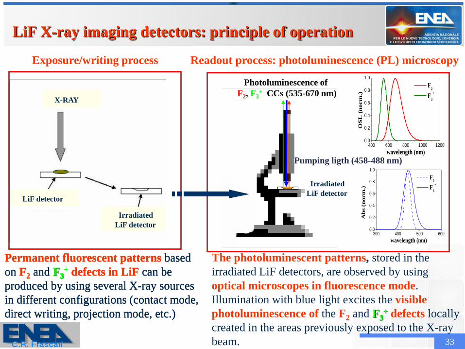
33
Irradiated
LiF detector
Pumping ligth (458-488 nm)
300 400 500 6000.0
0.2
0.4
0.6
0.8
1.0
Ab
s (
norm
.)
wavelength (nm)
F2
F3
+
Photoluminescence of
F2, F3+ CCs (535-670 nm)
400 600 800 1000 12000.0
0.2
0.4
0.6
0.8
1.0
OS
L (
norm
.)
wavelength (nm)
F2
F3
+
X-RAY
LiF detector
Irradiated
LiF detector
Permanent fluorescent patterns based
on F2 and F3+ defects in LiF can be
produced by using several X-ray sources
in different configurations (contact mode,
direct writing, projection mode, etc.)
The photoluminescent patterns, stored in the
irradiated LiF detectors, are observed by using
optical microscopes in fluorescence mode.
Illumination with blue light excites the visible
photoluminescence of the F2 and F3+ defects locally
created in the areas previously exposed to the X-ray
beam.
Exposure/writing process Readout process: photoluminescence (PL) microscopy
Permanent fluorescent patterns based
on F2 and F3+ defects in LiF can be
produced by using several X-ray sources
in different configurations (contact mode,
direct writing, projection mode, etc.)

Formation and stabilization of CCs: surface effects
34
The irradiation of alkali halide with ionizing radiation starts processes of defect creation and
diffusion which strongly affect the crystal surface. On the other hand, surface effects in
polycrystalline HA affects the formation and stabilization of color centers.
•The atomic coordination at the surface is not fully comparable to the atoms within a crystal.
•The surface atoms have neighbors on only one side, therefore they are less firmly bonded
than the internal atoms.
•They have broken bonds which make them more reactive.
•Mismatch between grains results in edge dislocations at the interface.
•Large disorder at the grain boundaries result in large gaps in the material.
However the possibilities for surface investigations of alkali halides, are quite restricted
because most of the standard surface-sensitive techniques, especially electron spectroscopies,
are difficult to use.
Edge dislocationsGrain boundaries