solid-state, 2-decade, 1.25kw linear amplifier binaries/january2015/development... · and homebrew...
TRANSCRIPT

Solid-state, 2-decade, 1.25kW Linear Amplifier
Andrew J. Buckler, K2OP
I’ve been a ham for almost 40 years now – starting young and going strong for the first 7 years or so, then a hiatus of about the same length for a quick stint back in, followed by a stretch of about 20 years with nary a contact. The first break was college and early married life, and the long stretch was due to a focus on raising the kids. But mid-life crises being as they are, and the kids starting to be off on their own, I decided to give it another go. I didn’t want to do just what I had done before, despite my complete enjoyment and wonderful memories of the HF experience. This time around, I wanted to build an EME station, try out the new-fangled software defined radio, have a decent system for satellites – and homebrew a solid state power amplifier to span the works. Frankly, I was less worried about homebrewing to save money as I was back in the 70’s, I wanted to do it because I just couldn’t find one that spanned what I needed, and searching for something that couldn’t be found increased a desire that the amplifier be more “mine” than it would be by purchasing. But saving money makes sense at any age, and the amplifier I put together wasn’t commercially available anyway. Maybe such a design will be of interest to some of you as well.

Contents
Goals and early phase of the project ............................................................................................................ 3
Tried to find an amp that already did this ................................................................................................ 3
Found the 2m amp, decided to use it as a base and build this thing myself ............................................ 3
High-level Design .......................................................................................................................................... 4
Tried to use reference designs from Freescale as a base ..................................................................... 4
Tried to use SPICE to create variants .................................................................................................... 5
Then I found the K7ES article and started a discussion with Communication Concepts: .................... 6
Ok, so the hardest part was over. Now I could proceed to the block diagram and high-level switching concepts ................................................................................................................................ 6
So I could finally start acquiring parts and building my amplifier! ............................................................... 8
First, get a base configuration working .................................................................................................... 8
VDD and Metering ................................................................................................................................ 8
Controller, ALC, and Attenuators .......................................................................................................... 9
2m deck itself, along with its T/R relays, LPF, and SWR detection ..................................................... 10
Good. The core concept works as hoped on 2m. Next, actually make the HF+6 idea work .................. 12
Input side ............................................................................................................................................ 12
Output side ......................................................................................................................................... 14
Degenerative Feedback – First Tortuous Considerations ................................................................... 15
Design I Actually Built – The First Time ............................................................................................... 16
HF+6 harmonic filters and SWR detection .......................................................................................... 19
Add the integrated power and control for weak signal receive ............................................................. 21
Packaging and cooling ............................................................................................................................. 22
Wiring diagram and final assembly ......................................................................................................... 26
Results ......................................................................................................................................................... 29
Amplifier Performance (before major re-work after 350 QSOs) ............................................................ 30
Operation with the Integrated Station ................................................................................................... 30
Problems Encountered and Overcome ................................................................................................... 31
Caveats, and Unfinished business (prior to robustness improvements discussed in postlog) ............... 32
Conclusions and Acknowledgements ......................................................................................................... 33
Postlog: ‘Twas Not the End of the Story! .................................................................................................... 33
Appendix: Detailed Bill of Material ............................................................................................................. 35
Appendix: Shack issues and integration ..................................................................................................... 35

Goals and early phase of the project
Early project objectives that I considered were as follows:
1. EME. My primary goal was to build an EME station. I knew that this meant some level of sophistication on both receive as well as transmit. Of course this meant I needed power at higher frequencies than I’d been accustomed to before. It also meant that I needed a separate receiver system where sequencing mattered because I had the combination of needing high isolation during transmit but very low loss with higher levels of sensitivity than I’d worked with before. In fact, I planned to use a cross-polarized receive system, so the T/R switching and other issues needed to be handled.
2. The “Magic Band” using SDR: My second goal started out to cover 6m robustly. This further drew me to a desire to give software-defined radio a try. I concluded that the Flex 1500 was a great way to get on 6 and experience SDR, but it only puts out 5 watts or less. I’ve never been a QRP guy – life is too short, so to speak – but the cost of the unit was right for the experience, and I was planning an amplifier anyway, right?
3. Small Footprint. I have always considered kW-plus amps to be bigger than I’d like, and since my searching and inquiries found no single amp that could span the range I wanted, I was up against two such beasts! That seemed wasteful of footprint, if not other components like the chassis, metering, cooling, power supply and distribution being doubled (or even tripled!). Think how silly that looks next to the Flex 1500. Why two when I considered my station as one?
Tried to find an amp that already did this
The first thing I did was to try to find a commercial amp that could span 2 and 6. I threw in 10m, because I always enjoyed that and was considering an antenna that was a 6/10 duobander. The range seemed reasonable, but it became clear that no single amp could be found, as there is a clear divide between HF and VHF, with 6 being on the HF side of this divide from the suppliers’ point of view: “Thanks for inquiring about my amplifiers. Unfortunately I will not be able to help you as I am not intending on building anything that operates below 144MHz.” … “I am sorry, you're going to need to find a different source. We do not have amplifiers that go up beyond 30 MHz.” … “Sorry, we are manufacturing only amplifiers that cover HF and 6m, or 1.8-50MHz, we don't have any VHF amplifier for 2m.” … “Unfortunately, we do not have an amplifier that covers all of those ranges.” … “Currently, we have individual amplifiers for 6m and 2m, but no combination amplifiers. Thanks for inquiring about our amplifiers - at this time we manufacture HF amplifiers that cover 160 m - 10 m and we also manufacture a standalone 6 m amplifier. We do not have any amps that cover 2 m.” … “So that I understand your request...are you looking for two amplifiers, with one able to power the other? We can provide that, but it will incur significant additional cost to do so. An alternative may be to purchase two amplifiers without power supplies, and for you to provide your own power supply and feed arrangement.” And on it went. I was not going to find what I wanted commercially. That’s when I decided to build it.
Found the 2m amp, decided to use it as a base and build this thing myself
As luck would have it – or was it meant to be? …the October 2012 issue of QST came out right when I was at the end of my rope looking for a commercial amp to meet the requirements. It had the article which ultimately won that month’s Cover Plaque Award, “Solid State 1 kW Linear Amplifier for 2 Meters,” by a very special person who has mentored me through much of the project: Jim Klitzing,

W6PQL.1 He described a Class AB amplifier that used a Freescale MRFE6VP61K25HR6 power FET with characteristics I was looking for – and with gain to spare.
The Kenwood TS-790A that I’m using on 2m generates up to 30W needs to get cut back by about 10 dB for the right drive. The 4 watt or so power output of the FlexRadio 1500 turns out to be perfect for this design – in fact, driving it with more requires attenuators that I included in the design, so no need to worry about any more! Even at these low levels, the maximum output power I’ve measured (skipping to the end of the story!) is about 1.4 kW. After going through T/R switches, filters and couplers, you can expect about 1.3 kW at saturation, and somewhat less at P1dB (output Power at 1 dB compression - the linear range. As long as I didn’t mind spending “a lot of time building one of these” - as Jim told me, “you'll wind up with a rock-solid amp that'll last a lifetime.”
I was on my way! … but of course I hadn’t really solved anything yet; there always were options for single bands. Making the decision to start from Jim’s components didn’t determine how I could support the range I wanted. But it gave me an elegant platform from which to develop, and that’s a big step forward. The thought going into the main project was to use Freescale parts to build two RF power decks, one for 144MHz and the other one spanning 28-54MHz, switching DC between the two decks, and RF at the output side between 28 and 54… but otherwise leveraging as much of the rest of the amplifier components as possible, including all control circuitry, power distribution, cooling, and mechanical packaging.
High-level Design
Basing my design from W6PQL components meant that my high-level design work was primarily geared to the low frequency deck(s). I also wanted to integrate more cross-polarization receive control support for EME, but the main even was getting the 10 and 6m part worked out. Of course the first naïve question was how far I could stretch it as-is, but Jim’s sweep had measured bandwidth at about 20 MHz for full power out. There just was currently no design for a kW amplifier that can span that entire range. HF amplifiers with broadband transformers can be built, but when you get to VHF and UHF, bandwidth and optimum match tend to be inversely proportional.
Tried to use reference designs from Freescale as a base
It made sense to start by asking Freescale what they thought. They post sample reference designs for this device as most manufacturers do, and would probably be willing to correspond with you on engineering matters.2 In addition to their reference design for 148MHz, they have reference designs for 40MHz and for 27MHz. As it happens, the approach was quite different for the two, with the 40 being similar to the VHF design but the 27 looking very different, similar to HF designs. The 40MHz design is right at the center of the range I wanted, which seemed promising, but it depended on the effective width of the response over my desired range. Aside from the length of the coax transformers and the ferrite core used on the input transformer, it's basically the same design as their reference design for 2m, and would adapt well to the components being used on the 2m deck. If that didn’t work, I reasoned that I could use two switchable stages, one presumably using the 27MHz reference design and another one moving the 40 to instead be centered at 50MHz (it would just be the 40MHz with coax transformers scaled for 6m). Once that is done, the next step could be to scale it for 28MHz. The input has a
1 www.w6pql.com 2 http://www.freescale.com/webapp/sps/site/prod_summary.jsp?code=MRFE6VP61K25H&nodeId=0106B9752000M20225

broadband transformer, and will no doubt just follow the output tuning. Another approach would be to start from the 27MHz reference that uses the ferrite core transformers commonly in use today for HF SSPA's, and try to scale them for 28-50MHz. Figure 1 shows one idea I had, to use the same input side and LDMOS, but have differently tuned output boards.
Figure 1: Initial concept for re-using input side and LDMOS but individual band output boards. Turned out not to be necessary. I wonder if it would have worked!
Since the coax transformers for 28MHz would be roughly twice as long as the 6m ones, a band switch might be as easy as shorting out the extra length on the 28MHz deck to put it on 6m. More specifically, roughly 25% of the output coax cable lengths from the LDMOS part of the board lead to the band switch. About 25% of the rest goes back to the board at the output balun connection point. The switch would connect the two together on 50 MHz, and route them through another roughly 50% of the total (for 28MHz) to put it back on 28 MHz. The same arrangement will have to be made for the output balun with another set of switch contacts. I contemplated developing a working 28MHz and a separate 50MHz pallet. Once that was done, I'd proceed to experimenting with switching on the 28MHz pallet. I didn’t want to end up with 3 pallets, but it seemed likely at this stage of the design process.
Tried to use SPICE to create variants
As an alternative to actually building all of the choices, I did some poking around to see if there was a relatively inexpensive way for me to get SPICE3 or ADS4, so that I could start from the 2m design (or the Freescale reference designs) and find component changes to make the lower frequencies work. There were two main subsystems of the amplifier that I needed to extend, the deck itself and the harmonic filters. Jim only provided a board for 144MHz, so I needed to create a version of them for 28 MHz and 50MHz. The core design issue I had was whether I could span the range 28-54MHz with one alternate or whether I would have to make dedicated ones for 28 and 50MHz. Means for switching and the coax baluns were the key components I needed to model. I knew I needed a very low loss switch or even a relay with high power handling for this to be possible. Everyone was telling me that it would be easier to just separately tune each reference board, to avoid sacrificing efficiency of the design. In any case, it seemed that it could be modeled in ADS, maybe not needing to model the traces but modeling the components (caps, coax/balun and switch). It seemed most sensible to start with the 40MHz design and then scale it up in frequency to get to 6m (and down to get to 10m) and put the switch electrical length into the model. Maybe I only needed to model the output matching network and not the LDMOS itself to come close.
3 http://en.wikipedia.org/wiki/SPICE 4 http://www.home.agilent.com/en/pc-1297113/advanced-design-system-ads?&cc=US&lc=eng

Then I found the K7ES article and started a discussion with Communication Concepts:
At about this timeframe, I became aware of the design concept originally described in 1990 by Helge Granberg, K7ES, in QEX that used Motorola MOSFETs.5 Figure 2 shows the schematic. 2-50MHz! Wow, I started out think I needed a separate deck for 10 and 6, this opened up the idea of only one deck all the way down to 160! Freescale’s 27MHz reference design seemed to use the basic approach (though I still don’t know why they present it as a narrow-band design), and Communication Concepts6 had various components and subsystems in a number of variations associated with the base design. The MOSFETs all these designs were using were older, and quite expensive compared to the Freescale device; I didn't see why the Freescale part couldn't be substituted on a single-device board using transformers rated for the correct power level. More specifically, if I could use elements from the W6PQL 2m deck, but with input and output transformers as well as RF capacitors from Communications Concepts, I would not only have a single deck that would span 28-54MHz, but in fact, one that would extend all the way down to 1.8MHz. Using the W6PQL PC boards provides regulated and temperature compensated bias, separated VDD feeds to the drain to keep high DC currents out of the RF transformers, and the same machined copper spreader and heat sink as the 2m deck (in fact, re-using the entire heat sink), so it met my leverage goals.
Figure 2: (part of) schematic from 1990 QEX article by K7ES
Rodger of Communications Concepts counseled me that these concepts were still experimental – with multiple issues remaining. “The SWR in the HF band is not very good. It gets worse at the low end of the band. 6m seems to be good. Good luck with the amplifier. The 820pf will certainly work and give some output. You might start with it and then try the 100pf. When I get back to the amplifier, I am going to try 300pf to see if there is much difference…” I decided not to be daunted, but rather to plunge right in.
Ok, so the hardest part was over. Now I could proceed to the block diagram and high-level switching concepts
With the outline in place for the RF design – two decks, with DC switching based on which was active, and re-use the rest – I proceeded to settle on the core components I needed to build. I left detailed design of each one until I was ready for it, but of course any system engineer knows how important it is to set the basic concepts in place before one find that the parts don’t mesh well. For example, I decided
5 Granberg, H. A Compact 1-kW 2-50 MHz Solid-State Linear Amplifier, QEX July 1990. 6 http://www.communication-concepts.com/

to use separate FET switches for the two decks for VDD (I knew from the start I would have some switching to do when the HF+6 and 144MHz decks are being used, and switching the “event 2” output from the controller to turn on the correct deck seemed appropriate). I also switched the bias, and a variety of other controls for the decks. I ended up arriving at three rocker switches and three rotary switches, as shown in Figure 4. The idea was to make it seem simple in use, as well as to leave as much on as possible for parallel operation, but not at the expense of risking equipment damage, such as leaving the highly sensitive EME receivers on and connected when they could be damaged.
Figure 3: Switching concept
Figure 4 identifies the components I had to build or integrate. I came to this based on my design objectives of course, and determined the system boundary so as to minimize the number of I/O with those components external to the amplifier.
Figure 4: High-level System Block Diagram
Ok, now it gets serious. Gotta buy some parts!
Controller
Cooling Ctl Sequencer
VSWR LockoutBias Reg
+12V Reg
VHF 144MHz (2m)LPF / SWR
Detect
RF Deck
Input Output
LDM
OS
VDD &
Displays
Weak Signal Receive Ctl
Preamp(s) & T/R Relays
Inp
ut Ou
tpu
t
HF+Six
RF Deck
Input Output
LDM
OS >20MHz (10/12/15m)
>12MHz (17/20m)>8MHz (30/40m)
>3MHz (60/75/80m)>1.5MHz (160m)
>55MHz (6m)
SWR
Det
ect
T/R Relays
Inp
ut
Ou
tpu
t
T/R Relays
HF+6 Transceiver
VHF Transceiver
HF+6 Antenna(s)
VHF Antennas
(cross-polarized)
Weak Signal Receiver
ALC
D
et
Att
enu
ato
rs
RF Control
+50V PSU
VDD
Key
System Boundary
So I could finally start acquiring parts and building my amplifier!
First, get a base configuration working
My approach was to establish a base of the core components, heavily influenced by those I could obtain from W6PQL initially and then work my way out from there.
VDD and Metering
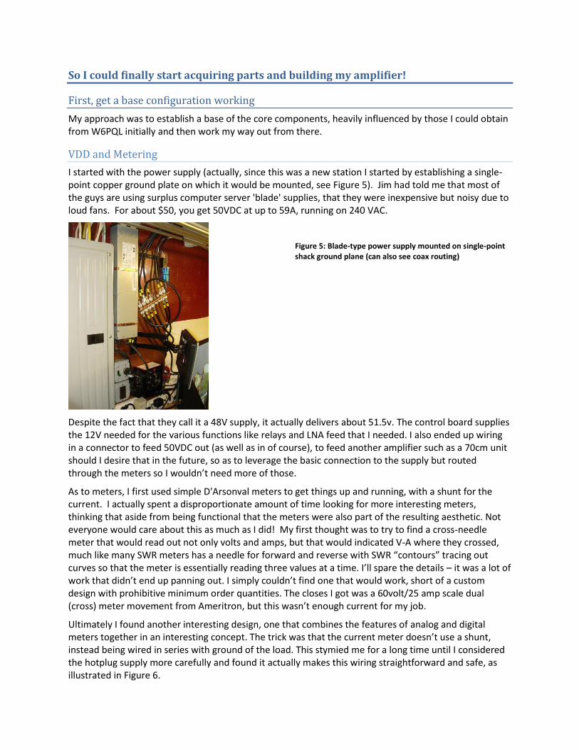
I started with the power supply (actually, since this was a new station I started by establishing a single-point copper ground plate on which it would be mounted, see Figure 5). Jim had told me that most of the guys are using surplus computer server 'blade' supplies, that they were inexpensive but noisy due to loud fans. For about $50, you get 50VDC at up to 59A, running on 240 VAC.
Figure 5: Blade-type power supply mounted on single-point shack ground plane (can also see coax routing)
Despite the fact that they call it a 48V supply, it actually delivers about 51.5v. The control board supplies the 12V needed for the various functions like relays and LNA feed that I needed. I also ended up wiring in a connector to feed 50VDC out (as well as in of course), to feed another amplifier such as a 70cm unit should I desire that in the future, so as to leverage the basic connection to the supply but routed through the meters so I wouldn’t need more of those.
As to meters, I first used simple D'Arsonval meters to get things up and running, with a shunt for the current. I actually spent a disproportionate amount of time looking for more interesting meters, thinking that aside from being functional that the meters were also part of the resulting aesthetic. Not everyone would care about this as much as I did! My first thought was to try to find a cross-needle meter that would read out not only volts and amps, but that would indicated V-A where they crossed, much like many SWR meters has a needle for forward and reverse with SWR “contours” tracing out curves so that the meter is essentially reading three values at a time. I’ll spare the details – it was a lot of work that didn’t end up panning out. I simply couldn’t find one that would work, short of a custom design with prohibitive minimum order quantities. The closes I got was a 60volt/25 amp scale dual (cross) meter movement from Ameritron, but this wasn’t enough current for my job.
Ultimately I found another interesting design, one that combines the features of analog and digital meters together in an interesting concept. The trick was that the current meter doesn’t use a shunt, instead being wired in series with ground of the load. This stymied me for a long time until I considered the hotplug supply more carefully and found it actually makes this wiring straightforward and safe, as illustrated in Figure 6.

Figure 6: PSu connection detail to amplifier and related meter wiring. LEFT: pinout of hotplug. RIGHT: wiring to meters.
Controller, ALC, and Attenuators
The W6PQL controller board is well described in Jim’s article and on his web site, so I’ll not spend many words on it here except to say it is one of the major factors I succeeded with the project. Basically I offloaded a great deal of design considerations and leveraged considerable expertise into this core component of the amplifier. It is small, elegant, and covers many functions and safety issues that are of substantial importance, and the small description here should simply be understood as my hat being off to him for it which allowed me the time to focus on other issues but based on a strong foundation.
I also used Jim’s ALC detector board. ALC back to the radio accomplishes two things...first, the control board uses it to keep the driving power minimal until your LNA gets out of the way, if you use one. Second, it prevents hot-switching of the input relay (driver power). Last, it is used as a safety to control drive level. As it happens, the Flex doesn’t have an ALC input, and they explain why.7 I’m still not convinced that it adds value for the complexity, based on other design features. But it is a second tier safety that doesn’t hurt and may help.
I also wanted to support a variety of input drive levels. Today I’m using the Kenwood and Flex, but maybe another rig will come along. I decided to build three into the amplifier, one for 10 dB (supporting input levels of up to 35 W), a 13.3 dB (supporting input levels up to 75 W), and a 15.5 dB (for up to 125 W). I got these from Jim too, but of course, as with all of the other components, I needed to determine where and how to mount them, as well as deal with the cabling. Not the hardest part of the design, but it had its own issues to confront and overcome as well! In particular, I needed to make decisions on internal coaxial cable specs,8 connectors, etc. I ended up using RG316 for the input side, and RG142 for the output side. 316 is easier to handle due to its smaller size and better flexibility, and mate well to SMA bulkhead cables/jacks. The RG142 is able to handle the power despite the fact that its cross-section is also rather small; but it is much less flexible than the 316. Figure 7 illustrates how the rear panel supports the various attenuator configurations and the range of input powers they enable.
7 http://kc.flex-radio.com/KnowledgebaseArticle50494.aspx 8 A good source for cable specifications is http://www.timesmicrowave.com/cgi-bin/calculate.pl

Figure 7: Flexible attenuator connections for multiple transceivers
2m deck itself, along with its T/R relays, LPF, and SWR detection
Of course, the real interest is in the RF decks. The idea was to start with the W6PQL components for 2m, in a “kit” form so that I was actually building it myself but with a lot of help. The first considerations were mechanical, considering such issues as where and where not to use solder, screws, and heat sink compound between the boards, the copper spreader, and the aluminum heat sink. No solder to hold the board to the spreader, the screws are enough. Heat sink compound between copper spreader and aluminum heat sink. Electrically, Figure 8 shows the schematic I built for the actual input and output side.
Figure 8: schematic for 2m power deck
One issue that gave me some difficulty was how to make a good thermal connection between the FET switch (a separate component that turns VDD on and off to the deck) and the heat sink, without inadvertently also making an electrical connection between VDD and ground. My concern stemmed from the fact that the sleeve portion of the shoulder washer doesn’t fully extend through both the

solder lug and transistor tab depths. It stops just into the tab. I knew that it avoided an outright short, but the space is so small between the screw shaft and the tab, in air since the insulator doesn’t go all the way, and there is a large current draw there at full VDD. To alleviate some of the concern, I wrapped the exposed portion of the screw with a bit of Teflon plumbers tape. Figure 9 shows the deck, the attenuators, the FET switch, the controller board (and another FET switch that would ultimately be used for the LNA relay control) prior to wiring.
Figure 9: Attenuators and 2m deck assembled and ready to be wired for testing. LEFT: top view. RIGHT: showing controller board mounting (front) and intended placement of HF deck (not yet assembled) rear.
Once assembled, the bias feed is wired for 12v in the chosen configuration, #14 wires carry the 50v to the VDD pads on the RF deck, and a liberal use of ferrite beads are used to keep RF out of the FET switch (those wires will pick some of it up otherwise). Along with the coax and T/R relays, it was ready for RF testing as shown in Figure 10.
Figure 10: Test set up used for initial RF testing. LEFT: close-up of deck. RIGHT: bench equipment.
Figure 10 shows the T/R relays as well as the 2m LPF board for harmonic rejection and integrated SWR detection (once again, provided by W6PQL). I used Tohtsu relays, model CX120A on the input, and CX600NL on the output. Whereas the connections on the CX600NL are N-Type, the connections to the CX120 are direct solder.

Of course it was exciting to perform the test! The test were carried out with two wattmeters, first before and after the attenuators, and then before and after the main RF deck. I first carefully brought up the attenuators, as shown in the left panel of Figure 11, comparing them with the ideal levels for the components used.
Figure 11: Test results. LEFT: Output power through each of the three attenuators, presented to input side of RF deck. RIGHT: Power output through the 2m deck.
The right panel of the figure is of course very satisfying, as it shows excellent gain, reaching the 1.25 kW design output I had hoped for!
Good. The core concept works as hoped on 2m. Next, actually make the HF+6 idea work
Coming off of the successfully building the 2m deck, I felt mentally prepared to undertake the detailed design of what I came to call the “HF+6” deck. Recall Figure 2; perhaps I could have just built it as is. But I was using a different LDMOS, and recall that I was hoping to avoid IC1 and the components around it, instead re-using the same controller board that I already had in place for the 2m deck.
Input side
Figure 12 shows the basic approach I took to thinking through the input side. The function performed by two separate blocks in the 2-50 design (right panel) are being performed by the boxed combination of parts in the 2m design. The difference is explained by the fact that the Granberg needed to have separate blocks to match the FETs which I wouldn’t need because both FETs are matched at the factory (in the same package). So I determined that I could just use a solo bias feed for both. Another observation is that the type of input transformer used in the 2m design had a tap that allowed me to eliminate the two 1k resistors and just use a 10 ohm resistor to feed the tap, as in the 2m bias arrangement. The actual transformer I was going to use would be different, and of course the 69 pF capacitor value needed to change.
0.00
0.50
1.00
1.50
2.00
2.50
3.00
0.0
2.5
5.0
7.5
10
.0
12
.5
15
.0
17
.5
20
.0
22
.5
25
.0
Dro
p (
rela
y an
d a
tte
nu
ato
r)
Input Power (watts)
Attenuator: Measured vs. Calculated
-10 dB
(calc)
-13 dB
(calc)
-15 dB
(calc) 0
200
400
600
800
1000
1200
1400
0 0.4 0.8 1.2 1.6 2 2.4 2.8 3.2 3.6 4
PA
Ou
tpu
t P
ow
er
Drive Power (after attenuator, if needed)
144MHz (2m) Deck
144MHz

Figure 12: Input design considerations. LEFT: Granberg design replicated components for separate circuit for each of the separate gates. RIGHT: the Klitzing design uses a common circuit, made possible since parts are matched as part of manufacturing process since they are in same package.
Many of the components from the Klitzing design could be used when their purpose wasn’t frequency dependent, like controlling the bias. An example of parts that are not frequency dependent is the 10 ohm resistor in Jim’s bias feed is replaced by the two 1k resistors, and then the same zener /thermistor /trimmer arrangement could be used. Figure 13 shows a component that is frequency dependent.
Figure 13: detailed consideration of part values and wiring. LEFT: 22 pF in parallel. RIGHT: 68 pF in series.
This part of the design is where Rodger really helped. We discussed use of the 68 versus 22, the value of C9, and whether C7 and C8 were necessary and how they related to the degenerative feedback components (see Figure 14). The 144MHz design couples the TUI-9 input transformer directly to the gates. The 2-50 design uses three capacitors, C7, C8 and C9. It would be easier not to use them, simply to use (either) the RF800-9-67 or TUI-9 without them, but presumably they were there are for a reason. My question was, was the reason due to the difference between the RF800-9-67 input transformer I was going to use for HF+6 versus the TUI-9 I had sued for the 2m (implying that they are needed with the former but not the latter), or were they needed due to the frequency range? If using the TUI-9 could allow me to avoid need for these components, then I would use the TUI-9. If they are needed anyway, then it doesn’t seem to matter much whether I would use the RF800 or the TUI-9, and I would make the decision based on whichever seems easiest to construct (see Degenerative Feedback section below).

Figure 14: coupling transformer to gates.
Rodger told me he tried a version of the amplifier with and without the two capacitors C7 and C8 and it made no difference that he could see, so I left them off as well. This was related to the choice I made regarding the degenerative feedback components in general. As to C9, I decided to use 100 pF instead of 820, but with an open question that maybe 300 might have been a better choice. Alas, this was to change after having used the amp for 350 QSOs or so, but I’m getting ahead of myself!
Output side
So I had decided to use the physical input board of Jim’s, but with a number of component changes. Now it was the time to decide on the output side. It seemed that unlike the input board which was almost completely re-useable, the output design was markedly different. The “good news” was that the 2-50 design seemed electrically if not mechanically simpler. As a major point of interpretation, I needed to decide whether to build the circuits on one of the sides of the 2m board and jumper to the corresponding pad on the other side, or build two copies of the C13/L3/C12/C10/C11 from the Granberg circuit, one per side, which seems to be more the approach taken in the 2m design. See Figure 15.
Figure 15: output side considerations for the HF+6 deck. LEFT: Granberg design for 2-50MHz. RIGHT: Klitzing design for 144MHz.
Further, apparently the RF 2067-9 which I had acquired from Communication Concepts only went up to 30MHz with the Teflon wire, but they had another one rated up to 80 MHz using coax windings rather than Teflon. The connection of +50VDD in the 2-50 design is L3, which performs the same function as the pair of 200n inductors in the 2m design. As a construction detail, my plan was to mount the RF2067-9 above C14 (which itself is actually two discrete capacitors tied together in an interesting way) as described in Granberg’s article, and support the other end with an insulting cable tie/mount towards the output coax connection at the far end of the board (which I abandoned ultimately, instead physically extending the board with a sawn piece from another one). Basically, I was trying to use as many of the

pads from the 2m board but according to the needs of the Granberg design rather than that which was intended when it is used for 2m.
Degenerative Feedback – First Tortuous Considerations
In Granberg’s design, there are components that connect the input to the output in a way different than in the 2m design. L1-R14 and L2-R15 provide degenerative feedback, apparently to keep the amplifier from oscillating at lower frequencies. These devices tend to have incredible gain at low frequencies, and require this feedback to lower it enough to be stable. The parts are typically mounted over the device ceramic from drain to gate. Figure 16 shows L1 and L2 on opposite sides – one on gate of FET, and the other on drain. Also, the part description says “15 nH, connecting wires to R14 and R15, 1.5 cm each #20 AWG,” implying that they are just wires, not even coiled.
Figure 16: Detailed consideration of coupling. LEFT RED: parts that did not appear on schematic. RIGHT RED: C7 and C8 physical placement. BLUE: components supporting degenerative feedback.
Clearly this part of the design would be tricky to build. I needed to devise a method to physically mount these parts in some fashion that connects the input and output boards with these parts mounted over the Freescale part. I thought of making this as a daughter board. C7 and C8 (each of which is actually a pair of 2200-pF) look like the main connection to the gates. As such, these are the connection between daughter board and main board. I proposed to mount them vertically between boards rather than horizontally on either board. Figure 17 shows what I came up with.
Figure 17: Proposed daughter board assembly procedure:
a. first, cut off end of a blank input board (taking advantage of fortuitous geometry),
b. then mount the two KDI resistors with adhesive (screws down to copper will be used later),
c. Then, mount the RF800, L1, and a straight wire to the daughter board
d. Then, mount the daughter board to the main input board (which had already been soldered to the FET gates and mounted to the copper spreader except for the 4 screws shown). Use ¼” spacers and longer screws to anchor to the spreader, providing thermal connection to the heat sink for the KDIs and
L1
a. b. c.

providing a physically robust mount)
e. Solder the four capacitors comprising C7 and C8 to electrically connect the daughter board to the underlying gate pads.
f. Add L2 and the non-inductor connection to the opposite sides of the KDIs to the drain pads on the output side.
Jim asked why I couldn’t “just use a 5w metal film resistor and a ceramic capacitor in series across the drain-to-gate connection…why do we bother with a daughter board?” Of course, I would like nothing more than to avoid the daughter board. But, I was thinking I needed it for two reasons: first, the transformer ends go through capacitors (C7 and C8) rather than directly to the gates. Second, the KDI resistors have flanges that look like they need to be attached thermally to the heatsink, because it seemed that they would get hot, given their values. The feedback resistors are very low in value, and because of this they will dissipate some power. If I were to keep that feedback system, I would use EMC parts, and heatsink them as shown in the figure. If I really did need the L1/R14 and L2/R15 parts, construction and mounting of the daughter board would be the last step in construction.
As it turns out, finding the resistors wasn’t easy, and when I did find them, they were expensive. This coupled with the complexity of the proposed construction suggested a path where I would build the deck without the feedback system, see if it oscillated, and add the feedback only if needed. Basically the whole thing rested on the assumption of need but it was possible to see if the need was real by using “safety” resistors on initial power up. The resistors go between the power supply and everything else with the purpose of dissipating power while the fuse gets hot enough to go, should the deck start to oscillate. I could remove them if everything comes up OK, and skip the whole feedback thing if I was lucky. Without giving away the whole story, I did get away with it for about 350 QSOs, but one day on 60m (running it at the reduced power level authorized there), something bad happened – “the smoke got out” – and I surmised that I needed the feedback. But this was well after putting the first build in place, so let’s get back to the story!
Design I Actually Built – The First Time
What remained were some physical issues about how to use the boards given all the part changes. Figure 18 shows some of the construction detail with the actual transformers I was using.
(RF800 not shown for simplicity, but it will be on according to step c)
L1
C7
C8
L2
d. and e. f.
(144MHz output shown, but of course this would be the 2-50 output instead)

Figure 18: pictorial outline of coupling through transformers and LDMOS
After all these considerations, I arrived at the schematic in Figure 19 for the initial build, with the expectation to add the degenerative feedback components should they be necessary but (perhaps naively) to avoid them if the circuit didn’t actually oscillate.
MRFE6VP61K25H
“T1” 9 to 1
Transformer
(RF800-3)
10
1000p
50
.1 u
22k10k
6v
200
Set IDQ
150250
330
Bias in
(12v)
1000p
“C10”
1000p
“C11”
1000p
“C12”
.1u
“C13”
.47u
Driver in
1.8-54 MHz 1.25 KW
Amplifier Stage
50v VDD
“T2” 1 to 9
Transformer
(RF2067C-LF-9)
“C9”
100p
1.25KW out
“L3”
10uH
22p
1000p
“C14”
NOTES
· Part numbers identified in quotes correspond with part numbers from
Granberg’s 1990 article. The 22p is also from Granberg but lacked a
designator in the 1990 article.
· Input side modeled after Klitzing design except 22p capacitor on input side of
T1 and 100p capacitor on output side of T1 are modeled after Granberg with
the exception that the value of C9 in Granberg is shown at 820p but the
alternate value of 100 is used in lieu of also using Granberg’s C7 and C8.
Figure 19: after design considerations, actual schematic with part values I used for the initial HF+6 build (but ‘twas not meant to last… see conclusions section!)
Figure 20 shows detail of the transformers connections to the LDMOS. C9 is the small part between the gates. The pair of metal film resistors that comprise C14 are hard to see, but the connection between drains and output transformer is through them, with the transformer physically mounting on top of them.

Figure 20: HF+6 design as first built (note LDMOS connections).
Figure 21 shows how I used a sawn extender board. The RG-142 coax output to the harmonic filters were ultimately connected to the sawn board extender.
Figure 21: HF+6 design as tested (note sawn board used to extend output side for length of transformer).
I used 6 50 ohm power resistors in parallel at initial power on. This worked out to just under 3 ohms at 300w or so. I was thrilled that I had no failed components at first turn-on, and no oscillations from the RF deck, so I removed the resistors and did the full power tests. No oscillation, even at full power! Figure 22 shows the results.
Figure 22: output of HF+6 deck as first built.
From the plots it is evident that the amplifier was “hottest” at 21 MHz. It may be clearly seen that both increases in frequency (up to 10 and 6) was well as down behave in roughly the same manner. The
0
200
400
600
800
1000
1200
1400
0 0.4 0.8 1.2 1.6 2 2.4 2.8 3.2 3.6 4
PA
Ou
tpu
t P
ow
er
Drive Power (after attenuator, if needed)
HF + Six Deck
50MHz
28MHz
21MHz
14MHz
7MHz
3.5MHz
1.8MHz

amplifier was very respectable at my original targets of 10 and 6, and in fact behaved well at all of the HF bands, even 160 though this was the weakest band. On the downside, the input match was very poor, even though there was apparently enough forward drive that the match still allows enough to drive to full power and a useful characteristic of the Flex is that they indicate the nature of the output stage tolerates even terrible matches, so in my case with this transceiver I did not have a problem. This wouldn’t be generally true however (see caveats and the design improvements implemented since this initial build in the conclusions.)
For what I was doing, a clearly exciting result!
HF+6 harmonic filters and SWR detection
My next challenge for the HF+6 portion was harmonic filtering. Associated with this is the manner of implementing the forward and reverse power measurements to drive the font panel and provide the SWR protection signal to the controller. One strategy was to have one that cuts out above 54 MHz and also integrates the power measurement, and then switch in additional ones for the bands below 6 to shift the cutoff frequency lower as needed. This idea seemed the most cost effective and compact. There were two alternative choices that seemed promising, one is from QST January 1983 by Granberg (specifically his Figure 5 on p. 31), and the second from February 1999 QST by Wetherhold W3NQN (starting on p. 44). Both seemed like they would work, but I knew I needed some help to figure it out and was pleased to receive it from Joel Hallas W1ZR and Ward Silver N0AX.
Joel: “Both filter designs look fine, but they are designed with different objectives -- and neither may be what is optimum for your design. Per FCC Part 97.307, all spurious outputs must be 43 dB below the level of the carrier. (60 dB below, if you include 6 meters, or any VHF band). The Wetherhold design (which requires an additional inductor per filter) is intended to maximize the reduction of the second harmonic, however, as noted in his footnotes, many amplifiers use a push-pull topology that tends to attenuate the second harmonic. For those amplifiers, it is often the third harmonic that has the highest amplitude -- for that case, the Wetherhold design is overkill or misfocused. I suggest that the way to start is to determine how much spurious content you have on each band without a filter. Then you will know how much attenuation you will need. In many cases, the use of near octave LPFs will be most cost effective since filters won't be required for each band. For example, a 5.5 MHz cutoff filter for 80/75, an 11 or 11.5 MHz cutoff for 40 and 30, a 23 MHz cutoff for 20, 17 and 15 and one at around 32 MHz for 12 and 10 might get you in spec for HF with only four filters. The necessary effectiveness of the filters will depend on the levels of the spurs, particularly on whether or not you have a large second harmonic component. The classic way is with a spectrum analyzer, It would be possible to use a communications receiver with a calibrated s-meter. In either case, you would want to have about 40 dB of attenuation between the amplifier and the measuring device. In any case, you will need this kind of setup in order to know that your amplifier is meeting specs -- so might as well have it early.”
Ward: “Filters basically reflect unwanted energy so it will be dissipated mostly in the generating devices - although you're not talking about a lot of energy here. Diplexers can divert harmonic energy to a resistive load and get rid of it that way instead of reflecting it. Either will work to reduce harmonic energy coming out of the amp. Joel is correct, though, in recommending that you measure what you actually have before selecting a filter family. Then you can choose the least expensive (usually also the most efficient) filter that will do the job.”
The bottom line was to get hold of a spectrum analyzer and see what the unfiltered amp was generating to inform the design. In setting out to do so, I had not initially appreciated how much work it would take! The measurements showed fairly low second harmonics due to the push-pull nature of the amplifier stage, but high enough to require sharp cutoffs if I was to support the WARC bands as I desired

and get it done in 6 banks. Having 6 banks is reasonably common, but few of the designs stretch it to 6 meters and support the WARC bands too. Splitting the bands into banks ended up as follows: 160, 80/75/60, 40/30, 20/17, 15/12/10, and 6. (Note that even though only limited power is allowed on 60 and 30, yet my drive was a QRP so generating 100-W and 200 watts respectively still required amplification, and 17 and 12 are full power bands.) The real issue was the third harmonic, though; in general, it was only down 10 dB down and on some bands only 8 dB down. Some authors (such as Sabin, 1999 July QEX) favored the diplexer design for solid state amps in the HF range because reflecting all that energy back into the output of the FETs risked driving the oscillations I had worried about in the detailed design of the power deck… I didn’t want to risk that either, so I chose the diplexer for all banks but the one for 6 m since the 3rd wasn’t so bad there). The problem was that no one had seemed to do this for high power (Sabin’s design was for 120-W). Poking around, I did find a high power set of diplexers by WB6DHW, and ultimately Dave proved very helpful, but I could not afford the amount of physical space it would have required for the multiple banks I needed, and his designs didn’t cover the WARC bands or 6m anyway. So I set about designing my own.
The steps I took were as follows:
1. Determination of actual requirements by measurement of harmonic levels using Rigol spectrum analyzer
2. Forward designs based on specifications derived from actual requirements using version 2.09 of the Tonne software for Chebyshev with passband ripple .005, T-type, >43 dB suppression for frequencies under 30MHz, 60 dB suppression for higher frequencies (I interpreted this conservatively at the frequency of the harmonic rather than the fundamental)
3. Determination of achievable part values iterated with simulation using RFSim99 software and coil turn calculations for various cores using K1QW software (accurate but not all cores supported) and online tool at toroids.info (less accurate but more supported cores)
4. Schematic capture and PCB layout using Diptrace (made considerably more difficult than at first expected due to the constraints I had on cabinet size)
5. Parts acquisition including relays, capacitors, inductor cores, wire, and custom PCB 6. Initial build and test using tracking generator on the Rigol, both forward insertion loss (to
measure filter response at fundamental and the needed harmonics) as well as return loss using 10 dB coupling attenuator (to derive VSWR at the fundamental and the harmonics).
7. Tuning! More Tuning! More Tuning! …virtually every part value changed… a fundamental flaw in my design settings had been that all the crossover and cutoff frequencies were too low, causing too much insertion loss and high VSWR in the passband. All but the 160 needed to be moved higher, but not so high as to provide inadequate suppression at the 2nd harmonic.
8. Determination of how to handle the SWR detection across the full range as well as interface to the controller board for load file using scheme that allowed switching between the decks
9. Testing at power, which resulted in burning out dump resistors and then more re-tuning! 10. Final integration test
It took me three full months to do this part of the project! Here’s where I ended up:
· 160m: 5 pole diplexer with crossover at 2.7 MHz with an added elliptical element on the LPF side. Note this design was scaled up from Sabin, but it is the only one I used because I could not get the simulation results to accord with his article for all the other bands so I couldn’t tell whether they would work or not but I did get simulated results that looked like I could use the 160, and I’m glad I did, because it worked).
· 80/75/60m: 5 pole diplexer with crossover at 6 MHz.
· 40/30m: 5 pole diplexer with crossover at 11 MHz.

· 20/17: 6 pole diplexer with crossover at 25MHz.
· 15/12/10: 7 pole diplexer with crossover at 42MHz.
· 6m: 6 pole LPF, cutoff at 65MHz, no HPF.
One of the most challenging parts of the HF harmonic filtering part of the project was making it fit in the chassis dimensions I had previously already set: of course, I probably should have left more room; but in order to make the measurements I needed to integrate components in a robust manner, which required that I set the dimensions before having the filters and I did my best to estimate what that would be prior to taking the measurements which resulted in the diplexer decision. A classic chicken and egg! But in the end, I made it work anyway, and with the challenge comes the satisfaction when the challenge is overcome.
Add the integrated power and control for weak signal receive
The weak signal receive chain that I was building for EME used two remote pre-amps (low noise amps, or LNAs) that needed power, with properly designed9 relays sequenced with the system. The relay design needs to achieve very low loss on receive (a few tenths of a dB makes a big difference, particularly in narrow bandwidth digital modes), but very high isolation on transmit.
I decided to use three separate feedlines from the linear to the LNA / relay box, one for transmit and one for each of the two receive polarizations, for maximum safety and reliability. I designed the control system in the amp to kill the relay power at PTT, placing the antenna on the TX transmission line. At no time are the LNAs in the transmission path. The relays on during receive, driven by a similar FET switch as is used to switch VDD to the RF decks, but with different values to switch 12 volts rather than 50. The high current capability of the switch is much more capacity than any LNA will need, but the FET switch is so inexpensive it may as well be used even though don’t need as much current for the LNA. The amp/bypass switch feeds the input of the FET switch, with a permanent jumper to the ‘on’ pad to ground. The control board (event 1) pulls the disable line low, removing LNA relay power during transmit. I also had to think through the various operating modes I wanted to support, cross-polarized operation with the pre-amps, single polarization without them, as well as think through how to leave as much running as possible without risking burned components in the highly sensitive receive chain, which meant also muting the matched receivers at various times but not others. Figure 23 illustrates additional details in the switching concept.
Figure 23: Detailed wiring of various controls affecting the weak-signal receive. LEFT: switching. RIGHT: cabling to feed system.
9 See http://www.w6pql.com/remote_LNA_controller.htm and other sources for design and construction aspects.

I also needed a clean power source for the highly sensitive receive components, and wanted a way to leverage the high current supply I already had feeding the amp. I knew that switching supplies create unwanted birdies, so I used a combination of a tightly-spec’ed DC/DC converter and a liberal usage of toroids which has achieved excellent results. Along with another current meter and display for this portion of the power distribution. The meter I chose was a multi-function unit that also had a temperature sensor, and since the W6PQL controller already had temperature inside the chassis covered, I decided to remotely mount the transducer to the output of the hotplug supply’s exhaust so that could be monitored too (Figure 24).
Figure 24: <TO BE CLEANED UP IF GO AHEAD WITH ARTICLE> Components use for powering and controlling weak-signal receive equipment
Packaging and cooling
I turned next to design the mechanicals, and along with that, decisions about the cooling. I used two types of fans, five along the back spanning the full heat sink as well as extra on each side for the various harmonics filters, and three somewhat smaller ones for each of the two RF decks and the attenuators which were lined up between them. Jim uses fewer, with the smaller chassis. My initial concept was to pull air in from a large vent in the rear panel, forced through the heat sink fins to the front panel area, and expelled through top cover vents. I later decided to make the top and sides not have vents, because I could get enough through the bottom, but this necessitated a switch to exhaust out the back with intake through the floor (Figure 25).
Figure 25: from left side looking right to show direction of the top and rear fans (not to scale)
Power decks and heat sink
Front
Rear

I run two of the three top fans, and two of the 5 bottom fans, whenever the controller is on. The others come on at transmit or when the thermistor shows overheating. I run fans at all times over the decks to ensure that dust never has a chance to collect, but in fact this may be overkill.
With the cooling in hand, I used rectangles in PowerPoint to do a rough layout. There were three dimensions to consider, using Jim’s basic concept of using Front Panel Designer10 to make the front, rear, and floor, and a simple folded piece for the sides and top. (I intentionally did a simpler project in this method prior to this project so that I had experienced the way this worked. I made a flexible interconnection box using the tool, and was quite pleased with the result but using this is very pricey. It is the difference between homebrew looking like homebrew versus looking more finished, so worth it to me. But others may choose differently.) The package with everything in it came to be 18” wide, 7” high, and 10” deep. I complained about the size to Jim, but he encouraged me by saying “but Andy, you have dragons in there!”
In fact, I actually made it a bit bigger than it needed to be, anticipating that I might put a tuner on top of it at some point, and the Palstar HF-AUTO11 (with stiff cables out the back) was near the size I was making so I just made it so that the tuner could fit on top if desired at some point. I did make it in the opposite orientation to many linears (and the tuner for that matter) because I preferred wide to deep. It makes for a very reasonable footprint in the shack.
Figure 26: view from top looking down (the PowerPoint I did was to scale, but the cut/pasted image here is not).
The floor plate design in Front Panel Designer (Figure 27), has a number of holes for a variety of mounting purposes, of course, along with the large intake vents for the cooling. I made it 5mm so as to have some good support stiffness, as it is a large piece. Each dimension, hole size, and construction detail required some concerted thought.
10 http://www.frontpanelexpress.com/ 11
http://www.palstar.com/en/hf-auto/
2m
Inp
ut
Relay
Power decks and heat sink
HF LPF’s on Rotary
LPF/
SWR
Det
LPF/
SWR
Det
A V
Switches and panel elements12v DC-DCconverter
RevPol.
VDD HF+
6In
pu
tR
elay
2mOutputRelay
HF+6
OutputRelay

Figure 27: floor plate in Front Panel Designer (not to scale)
For the rear, I set the thickness to 2mm as many of the rear-mounted connectors had limited thread lengths, but I would have preferred it to be stiffer than it came out since it is also rather large. It was a bit of a jigsaw puzzle to layout the rear because of part clearances, and I ended up making a mistake on the location of some of the SMAs for the attenuators and input relay connections. I was able to fix it and re-mark with yellow electrical tape, but it isn’t as elegant looking as it would have been without the mistake, since I took some care in doing etchings and connector labeling in the Designer (Figure 28).
Figure 28: rear panel in Front Panel Designer (not to scale
Of course these designs were iterated with the front panel, which needed to look good as well as being functional. I wanted it stiff, so I used 4mm thick, with powder coating and infilled-legends for the controls. This ended up being a difficult task, requiring two different cut-out rectangular regions on the reverse side of the panel to make the various control clearances work, as thread lengths, snap-in dimension, etc. all played a role. But based on my experience with making the rear panel 2mm, I am very glad I stuck to 4mm for the front. I would hate for it to feel “cheap” or under-designed when actuating the controls, and I’m happy with the result. Figure 29 and Figure 30 illustrate this panel.

Figure 29: view from front looking back (but without fans) (not to scale)
A lot of details had to come together, LEDs, bar graph display, rocker switches, blind holes for brackets and DC/DC converter, rotaries with keys and proper alignment of legends, the three meters, and the “title” or name of the amp. Unlike the rear panel where a little marked up tape can cover over mistakes, the front panel had to be perfect. At this time, there is one additional hole I am contemplating (to provide electronic switching between transmit polarization, which right now I have to swap cables to execute. As of this writing I am unsure whether to actually go ahead with the hole or do it another way so as not to mar the otherwise pristine appearance!
Figure 30: front panel in Front Panel Designer (not to scale)
On the cabinet cover, I make them myself; I have a small metal shear and a box-and-pan bending brake here. I can make you one, but we may need to discuss on the phone so I get the dimensions right, and can tell you how to align for proper fit and finish.
Last but not least was the folded panel for the top and sides. I had Front Panel Express make the three panels they were doing, and after inspecting them here, I shipped them to Jim in California who custom made this last piece and the bracketing (Figure 31 and Figure 32).
2mInputRelay HF
+6In
put
Relay
VDD in
Power decks and heat sink
A V
HF LPF’s on Rotary
LPF/
SWR
Det
LPF/
SWR
Det
OutputRelay
OutputRelay
Switches and panel elements
12v DC-DCconverter

Figure 31: The folded and assembled chassis assembly before painting the top and sides
We used 1/4" mesh for the grating over the vents, using machine screws where the bracket screws doubled for the grates and self-tapping sheet metal screws elsewhere.
Figure 32: after painting top but prior to electrical assembly
Wiring diagram and final assembly
One of the more satisfying parts of the project was the final assembly. Most (but not all) of the pieces had been individually assembled and tested, but final assembly required much of this to be pulled apart and put back together so I re-tested much of it as it came together. For example, Figure 33 illustrates that the first components to be put together was the 50V power distribution and metering, which was the very first thing I started with many months ago!

Figure 33: first wiring of power distribution and lower fans, followed by power test
I haven’t yet mentioned it in the article, but my daughter Mary had been a constant companion and helper throughout the project… becoming quite skilled in the process. Whereas Figure 34 shows her doing the front panel indicators, she was also responsible for some of the more demanding takss elsewhere as well.
Figure 34: main assembly of RF subsystem and front panel lights and switches

Figure 35 shows three views of the completed internals, including a small support cage for the 2m LPF board. It is important for the coils should be in the air stream of one of the cooling fans (they will run hot if not).
Figure 35: Assembled internal views NOTE TO REPLACE PHOTO AFTER HF HARMONIC FILTERS ARE DONE
After everything that had been done, it was actually a number of months between when I initially did the RF tests and the final assembly. The delay was for multiple reasons, not least because it took a while to do the mechanical design and get it all together, and I had spent quite a bit of time in the intervening period working on the receiver part of the shack and the antennas and rotator systems. Figure 36 shows the configuration as it stood for final test, and I was pleased that the RF performance was still what it had been.
Figure 36: final test
Actual wiring decisions were made throughout the project, but the initial block diagram proved reasonably effective as a guide. Figure 37 is where it ended up.
Figure 37: System wiring diagram
Results
Of course, the simplest way to assess the result is by taking a photo of the amplifier idling, and with the key down, and observing the difference. In fact, Figure 38 does just that. Judge for yourself!
Figure 38: installed in shack. LEFT: idling. RIGHT: “key down” (tongue in cheek, as the photo was taking while transmitting a JT65 cycle), 1.25kW

Amplifier Performance (before major re-work after 350 QSOs)
To augment the quantitative performance beyond the graphs provided earlier, Figure 39 provides combined efficiency and gain graphs across the (almost) 2-decade frequency range of the amplifier. 1.8MHz is not the amp’s strong suit, but it is functional there, and 6m isn’t great either. But it works even there as much as I need it to, and it is a real success everywhere else.
Figure 39: overall amp performance, 1.8MHz-144MHz (with harmonic filters in place)
Operation with the Integrated Station
Of course, the way it fits with other aspects of the shack is where the rubber hits the road. Figure 40 shows it together with the TS-790A, the FlexRadio 1500, the IQ+ matched receivers for cross-polarization EME, the rotator controller (which is powered by the amp), the hotplug and coax connections on the single-point ground plate, and software applications to run the various modes, including tracking of the moon and satellites with an integrated Google Earth view from the moon’s vantage point to boot!
Figure 40: integrated station
0
20
40
0 0.8 1.6 2.4 3.2 4
PA
Gai
n (
dB
)
Drive Power (after attenuator, if needed)
Amplifier Gain (both decks)
144MHz
50MHz
28MHz
21MHz
14MHz
0%
50%
100%
0 0.8 1.6 2.4 3.2 4
Effi
cie
ncy
Drive Power (after attenuator, if needed)
Efficiency (watts / volt-amps)
144MHz
50MHz
28MHz
21MHz
14MHz

The proof of the project being whether it could make contacts, I’m pleased to report that I made my first 9 EME contacts on July 4 and 5, 2013… about 10 months after starting the project; and my first HF contacts on October 9 and 12, 13 months into it.
Detailed bill of material and other specifics are in the extended material, but the bottom line on cost was about $3800. It could have been less with a few decisions, but this figure isn’t a bad one for budgetary purposes if you want to build one. And I think alternatives for cheaper would be hard to find.
Problems Encountered and Overcome
Defects corrected:
1. This project was the first time I did work with SMT, and I had a couple of part positioning problems and broken components. Figure 41 shows two problems on the output board of the 2m, where there's lots of energy. To remove the broken cap, I used two soldering irons, one on each side of the part. I also repositioned the 220uf, that looked dangerously close to shorting.
Figure 41: showing misplaced and damaged components. Note damaged SMT cap 2nd from right. LEFT: proper placement. RIGHT: improper placement.
2. Later, I burned out the power section on controller board. Specificially, the zener diode (D18) created a flash; when the TIP102 develops a collector-to-base short, it puts 50v at unlimited current across the Zener, and it opens up. These components were gone, and needed to be replaced. R1 was also out, as it feeds the power-on LED, and runs all the time, so if it had 50v on it, it wouldn't take very long to cook it. What may have caused this was a short on the 12v output of the board (perhaps an inadvertent one when experimenting), or even RF getting back into the TIP102. I re-worked so as to feed the TIP102 through an RF choke just to be safe, and the same for the 12v output from the board. I also added a limiting power resistor (20 ohms at 50w) in series with 50v to the TIP102 as a precaution...with this resistor in place, a short on the 12v line will limit the current and prevent a catastrophic failure.
3. I also had problems with the VDD FET switch of the HF+6 deck shorting to ground (twice: once when bringing it up initially, and then again at final assembly). I had a concern during assembly that there could be a short to ground since the shoulder insulator didn’t go all the way down the screw length because of the tab lug. I ultimately used Teflon tape around the screw on Jim’s suggestion, but then had to re-do it again on final assembly, so I hope it holds.
4. I also initially had poor performance on the HF+6 board, as I had mistakenly placed the input capacitor in series as it is in the 2m design, rather than in parallel, as the K7ES schematic shows

it. The cap prevented coupling of the lower frequencies, and moving the capacitor at Rodger’s suggestion opened it up nicely.
5. On final integration, I also had a problem with the switch components on LNA relay control. It wouldn’t switch into receive, and it turned out that I needed to replace three resistors to fix it. By that time, the unit was fully assembled and access to the resistors was tricky but possible.
6. As I pressed the EME station into operation, I had difficulty with burning FET switches. One problem was the placement, as I had the switch initially directly in a high field position, Also, I went through multiple iterations to determine how to best avoid shorting the main FET tab to ground while still having it attached to the heat sink. Also, I re-positioned the LPF board and included an enclosure for shielding. These changes appear stable as of this writing, with several hours of operation.
7. The HF harmonic filters had several issues in build, test, and operation. First, I had placed the cutoffs in the wrong spot, with too much passband loss. On some of the banks I had some of the fundamental going into the HPF and into the dump resistors, so I fried them quickly. Also, the design is not adequately protected for mistakes in bank selection (one band’s passband is another band’s stop band, so if you have the selector wrong things get fired). One thing I did was to make the dump resistors external for now so as to allow use of higher-power dump, but this wouldn’t be a great design were the amp to be mass produced. Also, presently I have the load fail indicator positioned before the diplexers to prioritize the protection of the power deck in the case where there is a problem in the HPF side as well as LPF, but as such, there is no detection to try to save the harmonic filters themselves in these circumstances. This trade-off would need to be re-visited, and presently it is very important to take care not to run it into a bad match or else have to open it up and replace burned filter caps. Which leads me to another issue, I used 500v micas but slowly but surely I am changing them to 1000v specs because they are more robust.
Caveats, and Unfinished business (prior to robustness improvements discussed in postlog)
I would note the following issues with what I did that ultimately could be addressed to make it even better:
1. The bad match for HF input would present difficulties for most drivers. The fact that I’m driving it with the FlexRadio that tolerates the match essentially gave me a “get out of jail free card” but this would not work for others. I haven’t done the experimentation to tell how hard it would be to fix but attention here is due.
2. Related to the above, I never did follow through with the modeling in Spice or ADS. Perhaps doing so would be a good approach rather than just experimentation. This might also help explore the lesser performance at the ends, 160 and 6. Once again, for me, it works well… but to truly make it a versatile design, this should be done.
3. The unit itself runs relatively quiet, even with the fans. In fact, it has a pleasant sound to it as it goes into transmit and turns on all the fans; it gives one the impression it is doing something without being annoying. The hotplug power supply, on the other hand, is too loud. Yes it was cheap; but if I had to do it over again, I would use a different supply to avoid this noise.
4. There are two functions that I would incorporate in a more complete design, well worth the effort based on the other positive aspects of the device. These would be full remote control, and also multiple antenna switching for the HF+6 deck. I don’t need remote control presently, and I have the HF+6 driving a 15/10/6 tribander at the moment, so these issues don’t slow me down. But the amp is worth these additional capabilities to make it of more general interest.

Conclusions and Acknowledgements
In conclusion, I have met all the goals I originally had, and had a great homebrewing experience in meeting them. The amplifier has a very wide range of functions, and the RF range is better than any other integrated device I’ve been able to find. It also looks great and has a form factor that fits well into the shack. Not only is the result what I hoped for, in fact the process has been just as satisfying as I have learned quite a bit and had the pleasure if interacting with a number of very helpful people that I’m pleased to know and work with. Specifically, I’d like to acknowledge the wonderful and over the top help I’ve received from Jim Klitzing W6PQL especially, but also Rodger, Joel Hallas W1ZR, and Ward Silver N0AX. Bob Allison WB1GCM of the ARRL provided super support in spectrum analyzer measurements, even visiting here at the shack which was an unsought but substantial pleasure. I had great help from Dave WB6DHW on the HF diplexers. I also owe a debt to Helge Granberg K7ES (s.k). Last but not least, I would like to thank my daughter Mary who has been an encouragement and physical help throughout the project, sharing in the excitement of what we’ve been able to do together.
Postlog: ‘Twas Not the End of the Story!
With the experience of running the amp for two months over about 350 QSOs, I made the following changes to harden the 160-2m SSPA which collectively improved the robustness and operating characteristics of the amplifier:
· Power deck improvements: o Fixed what had been a poor input VSWR (by changing input transformer and coupling to
gate components o Implemented a practical solution to degenerative feedback for robustness at low
frequency end
· Diplexer improvements: o Improved design of dump resistor by using alternative parts and a RF coupler fed into
detector to sense if bank selection is wrong o Beefed up capacitors to be more robust with load mismatches
· Misc. robustness fixes like part selection of FET switches, location of reflected power sense, etc.
With these changes, I have passed the 1100 QSO milestone with confirmed QSOs on 2, 6, 10, 12, 15, 17, 20, 30, 40, 60, 75, 80, and 160 (with output power set appropriately where it is limited) across AM, CW, SSB, and JT65 modes. Whereas one can never say it is beyond failure, it is at a relatively robust and useable stage now in any case.
Improved schematic for HF+6 power deck:

MRFE6VP61K25H
“T1” 4 to 1
Transformer
(Coax wound)
10
1000p
50
.1 u
22k10k
6v
200
Set IDQ
150250
330
Bias in
(12v)
1000p
“C10”
1000p
“C11”
1000p
“C12”
.1u
“C13”
.47u
Driver in
1.8-54 MHz 1.25 KW
Amplifier Stage
50v VDD
“T2” 1 to 9
Transformer
(RF2067C-LF-9)
1.25KW out
“L3”
10uH
22p
1000p
“C14”
NOTES
· Part numbers identified in quotes correspond with part numbers from
Granberg’s 1990 article. The 22p is also from Granberg but lacked a
designator in the 1990 article.
· Input side modeled after Klitzing design except 22p capacitor on input side of
T1 and 16 ohm resistor on output side of T1 in place of Granberg’s C9, C7,
and C8.
· Degenerative feedback approach simplified relative to Granberg.
16
500.05 u
500.05 u
Performance curves with this configuration:
0
200
400
600
800
1000
1200
1400
0 0.4 0.8 1.2 1.6 2 2.4 2.8 3.2
PA
Ou
tpu
t P
ow
er
Drive Power (after attenuator, if needed)
HF + Six Deck
50MHz
28MHz
21MHz
14MHz
7MHz
3.5MHz
1.8MHz

Appendix: Detailed Bill of Material
p/n’s, quantity, costs FILL IN IF THE ARTICLE GOES FORWARD
Appendix: Shack issues and integration
THIS SECTION MAY OR MAY NOT BE INCLUDED IN THE EXTENDED MATERIAL
Grounding
Magic box
15
20
25
30
35
0 0.4 0.8 1.2 1.6 2 2.4 2.8 3.2
PA
Gai
n (
dB
)
Drive Power (after attenuator, if needed)
Amplifier Gain (both decks)
144MHz
50MHz
28MHz
21MHz
14MHz
7MHz
3.5MHz
0%
20%
40%
60%
80%
0 0.4 0.8 1.2 1.6 2 2.4 2.8 3.2
Effi
cie
ncy
Drive Power (after attenuator, if needed)
Efficiency (watts / volt-amps)
144MHz
50MHz
28MHz
21MHz
14MHz
7MHz
3.5MHz

Figure 42: another project I did to help manage staion interconnect
Software applications
Weak signal box at bulkhead
Figure 43: Wiring diagram for weak-signal bulkhead box. (Many put the pre-amps on top of the tower.) (Note that xmt polarity switch not shown.)
Horizontal2M
Vertical2M
21/10/6m
70cm
LNA
LNA
Rotators
TO TOWER (outside)
TO SHACK(inside)
Output from linear
Vertical2M receiver
21/10/6m
70cm rig
Rotator controllers
Horizontal2M receiver
Sequencer out from linear
LNA power
1-5/8 heliax
1-5/8 heliax
1-5/8 heliax
LMR400
LMR400
LMR400
LMR400
LMR400
LMR400
LMR400
LMR400
Metal box mounted on cinder block foundation wall

Figure 44: construction of box
And of course, the antennas:
Figure 45: antennas