software vna and microwave network design and characterisation
TRANSCRIPT

Software VNA andMicrowave Network Design
and Characterisation
Zhipeng WuUniversity of Manchester, UK


Software VNA and Microwave NetworkDesign and Characterisation


Software VNA andMicrowave Network Design
and Characterisation
Zhipeng WuUniversity of Manchester, UK

Copyright © 2007 John Wiley & Sons Ltd, The Atrium, Southern Gate, Chichester,West Sussex PO19 8SQ, England
Telephone �+44� 1243 779777
Email (for orders and customer service enquiries): [email protected] our Home Page on www.wiley.com
All Rights Reserved. No part of this publication may be reproduced, stored in a retrievalsystem or transmitted in any form or by any means, electronic, mechanical, photocopying,recording, scanning or otherwise, except under the terms of the Copyright, Designs andPatents Act 1988 or under the terms of a licence issued by the Copyright Licensing AgencyLtd, 90 Tottenham Court Road, London W1T 4LP, UK, without the permission in writing ofthe Publisher. Requests to the Publisher should be addressed to the Permissions Department,John Wiley & Sons Ltd, The Atrium, Southern Gate, Chichester, West Sussex PO19 8SQ,England, or emailed to [email protected], or faxed to (+44) 1243 770620.
Designations used by companies to distinguish their products are often claimed astrademarks. All brand names and product names used in this book are trade names, servicemarks, trademarks or registered trademarks of their respective owners. The Publisher is notassociated with any product or vendor mentioned in this book.
This publication is designed to provide accurate and authoritative information in regard tothe subject matter covered. It is sold on the understanding that the Publisher is not engagedin rendering professional services. If professional advice or other expert assistance isrequired, the services of a competent professional should be sought.
Other Wiley Editorial Offices
John Wiley & Sons Inc., 111 River Street, Hoboken, NJ 07030, USA
Jossey-Bass, 989 Market Street, San Francisco, CA 94103-1741, USA
Wiley-VCH Verlag GmbH, Boschstr. 12, D-69469 Weinheim, Germany
John Wiley & Sons Australia Ltd, 42 McDougall Street, Milton, Queensland 4064, Australia
John Wiley & Sons (Asia) Pte Ltd, 2 Clementi Loop #02-01, Jin Xing Distripark, Singapore129809
John Wiley & Sons Canada Ltd, 6045 Freemont Blvd, Mississauga, ONT, Canada L5R 4J3
Wiley also publishes its books in a variety of electronic formats. Some content that appearsin print may not be available in electronic books.
Anniversary Logo Design: Richard J. Pacifico
British Library Cataloguing in Publication Data
A catalogue record for this book is available from the British Library
ISBN 978-0-470-51215-9 (HB)
Typeset in 10/12pt Galliard by Integra Software Services Pvt. Ltd, Pondicherry, IndiaPrinted and bound in Great Britain by TJ International, Padstow, CornwallThis book is printed on acid-free paper responsibly manufactured from sustainable forestry inwhich at least two trees are planted for each one used for paper production.

To Guoping, William and Richard


Contents
Foreword xv
Preface xvii
1 Introduction to Network Analysis of Microwave Circuits 1
1.1 One-Port Network 21.1.1 Total Voltage and Current Analyses 21.1.2 Transmission-Reflection Analysis 3
1.1.2.1 Voltage and current 31.1.2.2 Reflection coefficient 41.1.2.3 Power 51.1.2.4 Introduction of a1 and b1 51.1.2.5 Z in terms of � 7
1.1.3 Smith Chart 71.1.3.1 Impedance chart 71.1.3.2 Admittance chart 8
1.1.4 Terminated Transmission Line 91.2 Two-Port Network 10
1.2.1 Total Quantity Network Parameters 101.2.2 Determination of Z, Y and ABCD Parameters 111.2.3 Properties of Z, Y and ABCD Parameters 121.2.4 Scattering Parameters 121.2.5 Determination of S-Parameters 141.2.6 Total Voltages and Currents in Terms of a and b
Quantities 141.2.7 Power in Terms of a and b Quantities 141.2.8 Signal Flow Chart 15

viii CONTENTS
1.2.9 Properties of S-Parameters 151.2.10 Power Flow in a Terminated Two-Port Network 16
1.3 Conversions Between Z, Y and ABCD andS-Parameters 18
1.4 Single Impedance Two-Port Network 211.4.1 S-Parameters for Single Series Impedance 211.4.2 S-Parameters for Single Shunt Impedance 211.4.3 Two-Port Chart 22
1.4.3.1 Single series impedance network 221.4.3.2 Single shunt impedance network 231.4.3.3 Scaling property 25
1.4.4 Applications of Two-Port Chart 261.4.4.1 Identification of pure resonance 261.4.4.2 Q-factor measurements 271.4.4.3 Resonance with power-dependent losses 271.4.4.4 Impedance or admittance
measurement using the two-port chart 281.5 S-Parameters of Common One- and Two-Port
Networks 281.6 Connected Two-Port Networks 28
1.6.1 T-Junction 281.6.2 Cascaded Two-Port Networks 301.6.3 Two-Port Networks in Series and Parallel
Connections 311.7 Scattering Matrix of Microwave Circuits Composed of
One-Port and Multi-Port Devices 321.7.1 S-Parameters of a Multi-Port Device 321.7.2 S-Parameters of a Microwave Circuit 33
References 37
2 Introduction to Software VNA 39
2.1 How to Install 402.2 The Software VNA 412.3 Stimulus Functions 422.4 Parameter Functions 432.5 Format Functions 442.6 Response Functions 452.7 Menu Block 48
2.7.1 Cal 482.7.2 Display 482.7.3 Marker 512.7.4 DeltaM 532.7.5 Setting 542.7.6 Copy 55

CONTENTS ix
2.8 Summary of Unlabelled-Key Functions 552.9 Preset 562.10 Device Under Test 57
2.10.1 Device 592.10.2 Circuit 61
2.11 Circuit Simulator 632.11.1 Circuit Menu 632.11.2 Device Menu 642.11.3 Ports Menu 662.11.4 Connection Menu 67
2.12 Circuit Simulation Procedures and Example 67
3 Device Builders and Models 73
3.1 Lossless Transmission Line 743.2 One- and Two-Port Standards 763.3 Discrete RLC Components: One-Port Impedance Load 783.4 Discrete RLC Components: Two-Port Series
Impedance 793.5 Discrete RLC Components: Two-Port Shunt
Admittance 803.6 General Transmission Line 813.7 Transmission Line Components: Two-Port Serial
Transmission Line Stub 823.8 Transmission Line Components: Two-Port Parallel
Transmission Line Stub 833.9 Ideal Two-Port Components: Attenuator/Gain Block 853.10 Ideal Two-Port Components: 1:N and N:1
Transformer 863.11 Ideal Two-Port Components: Isolator 873.12 Ideal Two-Port Components: Gyrator 873.13 Ideal Two-Port Components: Circulator 883.14 Physical Transmission Lines: Coaxial Line 893.15 Physical Transmission Lines: Microstrip Line 903.16 Physical Transmission Lines: Stripline 943.17 Physical Transmission Lines: Coplanar Waveguide 963.18 Physical Transmission Lines: Coplanar Strips 983.19 Physical Line Discontinuities: Coaxial Line
Discontinuities 1013.19.1 Step Discontinuity 1013.19.2 Gap Discontinuity 1023.19.3 Open-End Discontinuity 103
3.20 Physical Line Discontinuities: Microstrip LineDiscontinuities 1043.20.1 Step Discontinuity 104

x CONTENTS
3.20.2 Gap Discontinuity 1073.20.3 Bend Discontinuity 1093.20.4 Slit Discontinuity 1103.20.5 Open-End Discontinuity 110
3.21 Physical Line Discontinuities: Stripline Discontinuities 1113.21.1 Step Discontinuity 1113.21.2 Gap Discontinuity 1143.21.3 Bend Discontinuity 1153.21.4 Open-End Discontinuity 116
3.22 General Coupled Lines: Four-Port Coupled Lines 1163.23 General Coupled Lines: Two-Port Coupled Lines 1173.24 Physical Coupled Lines: Four-Port Coupled Microstrip
Lines 1193.25 Physical Coupled Lines: Two-Port Coupled Microstrip
Lines 1223.26 Lumped Elements: Inductors 123
3.26.1 Circular Coil 1233.26.2 Circular Spiral 1253.26.3 Single Turn Inductor 126
3.27 Lumped Elements: Capacitors 1273.27.1 Thin Film Capacitor 1273.27.2 Interdigital Capacitor 129
3.28 Lumped Elements: Resistor 1293.29 Active Devices 1303.30 Antennas: Dipole Antenna 1303.31 Antennas: Resonant Antenna 1343.32 Antennas: Transmission Between Dipole Antennas 1353.33 Antennas: Transmission Between Resonant
Antennas 1363.34 User-Defined S-Parameters: One-Port Device 1373.35 User-Defined S-Parameters: Two-Port Device 138References 139
4 Design of Microwave Circuits 141
4.1 Impedance Matching 1414.1.1 Impedance Matching Using a Discrete
Element 1414.1.2 Single Stub Matching 1424.1.3 Double Stub Matching 143
4.2 Impedance Transformers 1454.2.1 Quarter-Wave Transformer 1454.2.2 Chebyshev Multisection Matching
Transformer 1464.2.3 Corporate Feeds 148

CONTENTS xi
4.3 Microwave Resonators 1494.3.1 One-Port Directly Connected RLC Resonant
Circuits 1494.3.2 Two-Port Directly Connected RLC Resonant
Circuits 1504.3.3 One-Port Coupled Resonators 1514.3.4 Two-Port Coupled Resonators 1524.3.5 Transmission Line Resonators 1544.3.6 Coupled Line Resonators 154
4.4 Power Dividers 1554.4.1 The 3 dB Wilkinson Power Divider 1554.4.2 The Wilkinson Power Divider with Unequal
Splits 1564.4.3 Alternative Design of Power Divider with
Unequal Splits 1574.4.4 Cohn’s Cascaded Power Divider 158
4.5 Couplers 1594.5.1 Two-Stub Branch Line Coupler 1594.5.2 Coupler with Flat Coupling
Response 1604.5.3 Three-Stub Branch Line Coupler 1614.5.4 Coupled Line Couplers 162
4.6 Hybrid Rings 1634.6.1 Hybrid Ring Coupler 1634.6.2 Rat-Race Hybrid 1644.6.3 Wideband Rat-Race Hybrid 1644.6.4 Modified Hybrid Ring 1654.6.5 Modified Hybrid Ring with Improved
Bandwidth 1654.7 Phase Shifters 166
4.7.1 Transmission Line Phase Shifter 1664.7.2 LC Phase Shifters 167
4.8 Filters 1684.8.1 Maximally Flat Response 1684.8.2 Chebyshev Response 1684.8.3 Maximally Flat Low-Pass Filters with �c = 1 1694.8.4 Chebyshev Low-Pass Filters with �c = 1 1714.8.5 Filter Transformations 1724.8.6 Step Impedance Low-Pass Filters 1734.8.7 Bandpass and Bandstop Filters Using �/4
Resonators 1744.8.8 Bandpass Filters Using �/4 Connecting Lines
and Short-Circuited Stubs 1754.8.9 Coupled Line Bandpass Filters 1764.8.10 End-Coupled Resonator Filters 178

xii CONTENTS
4.9 Amplifier Design 1794.9.1 Maximum Gain Amplifier Design 1794.9.2 Broadband Amplifier Design 1814.9.3 High-Frequency Small Signal FET Circuit
Model 1824.9.4 Negative Feedback Amplifier Design 183
References 185
5 Simulation of Microwave Devices and Circuits 187
5.1 Transmission Lines 1885.1.1 Terminated Transmission Line 1885.1.2 Two-Port Transmission Line 1895.1.3 Short-Circuited Transmission Line Stub 1895.1.4 Open-Circuited Transmission Line Stub 1905.1.5 Periodic Transmission Line Structures 192
5.2 Impedance Matching 1945.2.1 Matching of a Half-Wavelength Dipole Antenna
Using a Discrete Element 1945.2.2 Single Stub Matching of a Half-Wavelength
Dipole Antenna 1955.3 Impedance Transformers 197
5.3.1 Quarter-Wave Impedance Transformer 1975.3.2 Chebyshev Multisection Impedance
Transformer 1985.3.3 Corporate Feeds 1995.3.4 Corporate Feeds Realised Using Microstrip
Lines 2015.3.5 Kuroda’s Identities 201
5.4 Resonators 2055.4.1 One-Port RLC Series Resonant Circuit 2055.4.2 Two-Port RLC Series Resonant Circuit 2055.4.3 Two-Port Coupled Resonant Circuit 2085.4.4 Two-Port Coupled Microstrip Line
Resonator 2085.4.5 Two-Port Coupled Microstrip Coupled Line
Resonator 2105.4.6 Two-Port Symmetrically Coupled Ring
Resonator 2125.4.7 Two-Port Asymmetrically Coupled Ring
Resonator 2135.5 Power Dividers 213
5.5.1 3 dB Wilkinson Power Divider 2135.5.2 Microstrip 3 dB Wilkinson Power Divider 2165.5.3 Cohn’s Cascaded 3 dB Power Divider 217

CONTENTS xiii
5.6 Couplers 2195.6.1 Two-Stub Branch Line Coupler 2195.6.2 Microstrip Two-Stub Branch Line Coupler 2215.6.3 Three-Stub Branch Line Coupler 2215.6.4 Coupled Line Coupler 2225.6.5 Microstrip Coupled Line Coupler 2255.6.6 Rat-Race Hybrid Ring Coupler 2255.6.7 March’s Wideband Rat-Race Hybrid Ring
Coupler 2265.7 Filters 229
5.7.1 Maximally Flat Discrete Element Low-PassFilter 229
5.7.2 Equal Ripple Discrete Element Low-PassFilter 231
5.7.3 Equal Ripple Discrete Element BandpassFilter 232
5.7.4 Step Impedance Low-Pass Filter 2335.7.5 Bandpass Filter Using Quarter-Wave
Resonators 2365.7.6 Bandpass Filter Using Quarter-Wave
Connecting Lines and Short-Circuited Stubs 2365.7.7 Microstrip Coupled Line Filter 2395.7.8 End-Coupled Microstrip Resonator Filter 241
5.8 Amplifier Design 2415.8.1 Maximum Gain Amplifier 2415.8.2 Balanced Amplifier 245
5.9 Wireless Transmission Systems 2455.9.1 Transmission Between Two Dipoles with
Matching Circuits 2455.9.2 Transmission Between Two Dipoles with an
Attenuator 249References 249
Index 251


Foreword
Software VNA and Microwave Network Design and Characterisationis a unique contribution to the microwave literature. It fills a needin the education and training of microwave engineers and builds uponwell-established texts such as Fields and Waves in CommunicationElectronics by S. Ramo, J. Whinnery and T. Van Duzer, Foundations forMicrowave Engineering by R.E. Collin and Microwave Engineering byD. Pozar. The ‘virtual vector network analyser’ that can be downloadedfrom the CD supplied with the book enables those without accessto a real instrument to learn how to use a vector network analyser.The many design examples provide opportunities for the reader tobecome familiar with the Software VNA and the various formatsin which frequency responses can be displayed. They also encourage‘virtual experiments’.
Design formulas for many devices are given, but the underlying theorythat can be found in other texts is not covered to avoid repetition. A circuittheory or field theory approach is available and this encourages the userto link the two. A novel feature of the book is the introduction andapplication of a two-port chart that complements the well-known Smithchart, widely used for one-port circuits. The two-port chart enables thefrequency response of transmission parameters to be displayed as well asreflection parameters. The range of devices introduced in the book includesstubs, transformers, power dividers/combiners, couplers, filters, antennasand amplifiers. Nonideal behaviour, e.g. the effects of dielectric, conductorand radiation losses, is included for many devices. The devices can beconnected to form microwave circuits and the frequency response of thecircuit can be ‘measured’. The lower frequency limit in the Software VNAis 1 Hz and circuits containing both lumped and distributed devices can becharacterised.
Assuming a knowledge of transmission lines, circuits and someelectromagnetic theory, Software VNA is suitable for introduction at the

xvi FOREWORD
final-year undergraduate level and postgraduate levels. Students would bestimulated by the opportunity to ‘measure’ their own devices and circuits.Experienced microwave engineers will also find Software VNA useful.
L.E. DavisUniversity of Manchester

Preface
In addition to conventional textbooks, the advances in computer technologyand modern microwave test instruments over the past decade havegiven electrical engineers, researchers and university students two newapproaches to study microwave components, devices and circuits. TheVector Network Analyser (VNA) is one of the most desirable instrumentsin the area of microwave engineering, which can provide fast and accuratecharacterisation of microwave components, devices or circuits of interest.On the other hand, a commercial microwave circuit simulation softwarepackage offers a cost-effective way to study the properties of microwavecomponents and devices before they are used to construct circuits andthe properties of the circuits before they are built for testing. However,mainly due to their costs, VNAs and microwave circuit simulators arenot widely accessible on a day-to-day basis to many electrical engineers,researchers and university students. This book together with the associatedsoftware is intended to fill in the gap between these two aspects with (i)an introduction to microwave network analysis, microwave componentsand devices, microwave circuit design and (ii) the provision of both deviceand circuit simulators powered by the analytical formulas published in theliterature.
The purpose of the associated software named Software VNA is fourfold.First, it functions as a VNA trainer with a lower frequency limit of 1 Hz anda upper frequency limit of 1000 GHz, providing to those who have not seenor used a VNA before the opportunity to have personal experience of how aVNA would operate in practice and be used for microwave measurements.Secondly, it provides experienced users with an option to get access to thedata on a commercial VNA test instrument for data analysis, manipulationor comparison. Thirdly, it provides the users with a simulator equippedwith 35 device builders from which an unlimited number of devices can bedefined and studied. Analytical CAD equations, many of which have beenexperimentally verified, are used as models for simulation, giving no hidden

xviii PREFACE
numerical errors. The users may also use the Software VNA to verify thelimitations and accuracy of the CAD equations. Finally, it provides the userswith a circuit simulator that they can use to build circuits and study theirproperties.
The book has five chapters. In Chapter 1, the basic theory of networkanalysis is introduced and network parameters are defined. In Chapter 2,the installation and functions of the Software VNA are described. InChapter 3, the built-in device models are presented with detailed equationsand their limitations. In Chapter 4, circuit design and operation principlesfor impedance matching, impedance transformation, resonators, powerdividers, coupler, filters and amplifiers are summarised, and the designexamples of these circuits are given in Chapter 5.
The book and its associated software can be used for teaching in the areaof microwave engineering.

1Introduction to NetworkAnalysis of MicrowaveCircuits
ABSTRACT
Network presentation has been used as a technique in the analysis of low-frequency electrical and electronic circuits. The same technique is equallyuseful in the analysis of microwave circuits, although different networkparameters are used. In this chapter, network parameters for microwavecircuit analysis, in particular scattering parameters, are introduced togetherwith a Smith chart for one-port networks and a new chart for two-portnetworks. The analyses of two-port connected networks and a circuitcomposed of multi-port networks are also presented.
KEYWORDS
Network analysis, Network parameters, Impedance parameters, Admittanceparameters, ABCD parameters, Scattering parameters, Smith chart, Two-port chart, Connected networks
Network presentation has been used as a technique in the analysis oflow-frequency electrical and electronic circuits (Ramo, Whinnery and vanDuzer, 1984). The same technique is equally useful in the analysis ofmicrowave circuits, although different network parameters may be used(Collin, 1966; Dobrowolski, 1991; Dobrowolski and Ostrowski, 1996;Fooks and Zakarev, 1991; Gupta, Garg and Chadha, 1981; Liao, 1990;Montgomery, Dicke and Purcell, 1948; Pozar, 1990; Rizzi, 1988; Ishii1989; Wolff and Kaul, 1998). Using such a technique, a microwave circuit
Software VNA and Microwave Network Design and Characterisation Zhipeng Wu© 2007 John Wiley & Sons, Ltd

2 INTRODUCTION TO NETWORK ANALYSIS
can be regarded as a network or a composition of a number of networks.Each network may also be composed of many elementary components. Anetwork may have many ports, from which microwave energy flows intoor out of the network. One- and two-port networks are, however, the mostcommon, and most commercial network analysers provide measurementsfor one- or two-port networks. In this chapter, the network analysis will bebased on one- and two-port networks. Network parameters, in particularscattering parameters, will be introduced together with a Smith chart forone-port networks and a new chart for two-port networks. The analysis oftwo connected networks and a circuit composed of a number of networkswill also be presented. For further reading, see references at the end of thechapter.
1.1 ONE-PORT NETWORK
A one-port network can be simply represented by load impedance Z tothe external circuit. When the network is connected to a sinusoidal voltagesource with an open circuit peak voltage Vs and a reference internalimpedance of Z0�ref as shown in Figure 1.1, the circuit can be analysed usingthe circuit theory based on total voltage and current quantities. It can alsobe analysed using the transmission-reflection analysis based on incident andreflected voltage and current quantities. Both analyses are described below.The reference internal impedance Z0�ref of the source is assumed to be 50 �throughout this book.
1.1.1 Total Voltage and Current Analyses
Using circuit theory, the voltage V on the load impedance and the currentI flowing through it as shown in Figure 1.1 are related by
V = ZI �1.1�
ZVVs
Z0,ref
I
Figure 1.1 Simplified one-port network

ONE-PORT NETWORK 3
and they can be obtained by
V = VsZ
Z0�ref +Z�1.2a�
and
I = Vs
Z0�ref +Z� �1.2b�
The power delivered to the load impedance by the voltage source can beobtained by
PL = 12
Re�VI∗� = �Vs�22�Z0�ref +Z�2 Re�Z�� �1.3�
where ∗ indicates the complex conjugate.
1.1.2 Transmission-Reflection Analysis
1.1.2.1 Voltage and current
Using the transmission-reflection analysis, the incident voltage V + is definedto be the voltage that the voltage source could provide to a matched load,i.e. when Z = Z0�ref , and the incident current I+ to be the correspondingcurrent flowing through the matched load. Hence
V + = Vs
2�1.4a�
and
I+ = V +
Z0�ref= Vs
2Z0�ref� �1.4b�
Therefore if ZL = Z0�ref , then V = V + and I = I+. However, in the generalcase that Z �= Z0�ref , the voltage V can be taken to be the superposition oftwo voltages: the incident voltage V + and a reflected voltage V −. Similarlythe current I can be taken as the superposition of two currents: the incidentcurrent I+ and a reflected current I−. Since V can be written as V = IZ0�ref +Ve with
Ve = Vs�Z −Z0�ref�
Z +Z0�ref� �1.5�

4 INTRODUCTION TO NETWORK ANALYSIS
V
– V
+
Vs Ve
Z0,refZ0,ref
I
– I
+
Figure 1.2 Equivalent circuit
the circuit in Figure 1.1 can be represented by an equivalent circuit shownin Figure 1.2. The load impedance Z is replaced by a ‘voltage source’ Vewith an ‘internal impedance’ Z0�ref . By using the superposition theorem, thereflected voltage can be taken to be that produced by the equivalent voltagesource Ve so that
V − = Ve
2= Vs
2�Z −Z0�ref�
�Z +Z0�ref��1.6a�
and
I− = V −
Z0�ref= Vs
2Z0�ref
�Z −Z0�ref�
�Z −Z0�ref�� �1.6b�
The total voltage and current are then
V = V + +V − = Vs
Z0�ref
Z +Z0�ref�1.7a�
and
I = I+ − I− = Vs1
Z +Z0�ref� �1.7b�
which are the same as those in Equation (1.2) obtained using circuit theory.
1.1.2.2 Reflection coefficient
Using the transmission-reflection analysis, the total voltage is expressed asthe sum of the incident voltage and the reflected voltage, and the currentas the difference of the incident current and the reflected current. For theconvenience of analysis, a reflection coefficient can be introduced to relatethe reflected and incident quantities. The reflection coefficient is defined as
� = V −
V + = I−
I+ = Z −Z0�ref
Z +Z0�ref= Y0�ref −Y
Y0�ref +Y� �1.8�

ONE-PORT NETWORK 5
where Y0�ref = 1/Z0�ref and Y = 1/Z and is defined with respect to thereference impedance Z0�ref .
The total voltage and current at the load can then be expressed as
V = V +�1+�� �1.9a�
and
I = I+�1−��� �1.9b�
Hence the total voltage and current quantities can be obtained when � isdetermined.
1.1.2.3 Power
Associated with the incident voltage V + and the incident current I+ is theincident power which is given by
P+ = 12
Re�V +I+∗� = 12
�V +�2Z0�ref
= �Vs�28Z0�ref
= Pmax� �1.10�
This power is also the maximum power available from the voltage source.Similarly the reflected power is associated with the reflected voltage V − andthe reflected current I− and is given by
P− = 12
Re�V −I−∗� = 12
�V −�2Z0�ref
= Pmax�� �2� �1.11�
The power delivered to the load impedance is the difference between theincident power and the reflected power, i.e.
PL = P+ −P− = P+�1−�� �2�� �1.12�
which is identical to Equation (1.3).
1.1.2.4 Introduction of a1 and b1
Since the incident power is related to V + and Z0�ref and the reflected powerto V − and Z0�ref as in Equations (1.10) and (1.11), their expressions can besimplified with the introduction of two new quantities a1 and b1 which aredefined as (Collin, 1966; Pozar, 1990)
a1 = V +√Z0�ref
�1.13a�

6 INTRODUCTION TO NETWORK ANALYSIS
and
b1 = V −√Z0�ref
� �1.13b�
Using these two new quantities, the incident, reflected and total powerscan then be expressed, respectively, as
P+ = 12
�a1�2� �1.14a�
P− = 12
�b1�2 �1.14b�
and
PL = 12
��a1�2 −�b1�2�� �1.14c�
The voltage and current quantities can also be written as
V + = a1
√Z0�ref� �1.15a�
V − = b1
√Z0�ref� �1.15b�
I+ = a1√Z0�ref
� �1.15c�
I− = b1√Z0�ref
� �1.15d�
V = �a1 +b1�√
Z0�ref �1.15e�
and
I = a1 −b1√Z0�ref
� �1.15f�

ONE-PORT NETWORK 7
The reflection coefficient defined in Equation (1.8) becomes
� = b1
a1= Z −Z0�ref
Z +Z0�ref= Y0�ref −Y
Y0�ref +Y� �1.16�
Using a1 and b1, the signal reflection property of the one-port networkcan be described by
b1 = �a1� �1.17�
1.1.2.5 Z in terms of �
The formulas derived above are useful for the analysis of one-port networkwhen the load impedance is known. However, very often in practice, Z hasto be determined from measurement. In this case, Z can be obtained fromthe measurement of the reflection coefficient using
Z = 1+�
1−�Z0�ref� �1.18�
1.1.3 Smith Chart
1.1.3.1 Impedance chart
The impedance Smith chart (Smith, 1939, 1944) is based on the expressionof the reflection coefficient � in terms of load impedance Z. With theintroduction of the normalised load impedance with respect to the referenceimpedance Z0�ref as
z = Z
Z0�ref= r + jx� �1.19�
where r and x are the normalised resistance and reactance, respectively, thereflection coefficient � can be written as
� = z−1z+1
= r + jx−1r + jx+1
= u+ jv� �1.20�
where u and v are the real and imaginary projections of � on the complexu–v plane. Equation (1.20) can be rearranged to give the following twoseparate equations:
(u− r
1+ r
)2
+v2 = 1�1+ r�2
�1.21a�

8 INTRODUCTION TO NETWORK ANALYSIS
and
�u−1�2 +(
v− 1x
)2
= 1x2
� �1.21b�
Equation (1.21a) represents a family of constant resistance circles. Thecentre of the circle for a normalised resistance r is at (r/�1+ r��0) and theradius is 1/�1+r�. Equation (1.21b) describes a family of constant reactancecircles. The centre of the circle with a normalised reactance x is at �1�1/x�and the radius of the circle is 1/�x�. A simplified impedance Smith chart isshown in Figure 1.3. On the chart, the normalised resistance and reactancevalues, r and x, can be read when the reflection coefficient � is plotted. Onthe other hand, the complex reflection coefficient can be determined whenr and x values are known and plotted on the impedance chart.
1.1.3.2 Admittance chart
With the introduction of the normalised admittance
y = Y
Y0�ref= g + jb� �1.22�
where g and b are the normalised conductance and admittance, respectively.Equation (1.16) for the reflection coefficient � can be rearranged to
−� = g + jb−1g + jb+1
� �1.23�
–2
–1
–0.5
210.5
2
1
0.5
r = 0x = 0 r = ∞
Figure 1.3 Simplified Smith chart

ONE-PORT NETWORK 9
Comparing Equation (1.23) with Equation (1.20), it can be seen thatg would be the same as r and x as b if � in Equation (1.20) is replacedby −� . Hence the admittance Smith chart can be obtained by rotating theimpedance chart by 180�. Alternatively the values of g and b can be readon the impedance chart as for r and x by plotting −�L on the impedancechart.
1.1.4 Terminated Transmission Line
For a terminated transmission line, as shown in Figure 1.4, the voltage andcurrent at any position on the transmission line can be described by thefollowing two equations:
V�z� = V +e−�z +V −e�z = V +�e−�z +�Le�z� �1.24a�
and
I�z� = I+e−�z − I−e�z = V +
Z0�e−�z −�Le�z�� �1.24b�
where Z0 is the characteristic impedance of the transmission line, �L thereflection coefficient with respect to the transmission line impedance of Z0
and � the propagation constant. The reflection coefficient �L is given by
�L = ZL −Z0
ZL −Z0�1.25a�
and the propagation constant by
� = + j = �c +d +r�+ j�
vp� �1.25b�
where is the attenuation constant in Nepers/m, the phase constant inrad/m and vp the phase velocity. The attenuation constant may consist of
Z0γ = α + jβ ZLZin
z = –L z = 0z
Figure 1.4 Terminated transmission line
10 INTRODUCTION TO NETWORK ANALYSIS
three parts: c for conducting loss, d for dielectric loss and r for radiationloss. The dielectric loss d can be expressed as
d = 12
tan�� �1.26�
where tan � is the loss tangent of the dielectric material used in thetransmission line.
The input impedance of the transmission line of length L can be obtainedby
Zin = Z0ZL +Z0 tanh��L�
Z0 +ZL tanh��L�� �1.27�
If the terminated transmission line is connected to a sinusoidal voltagesource with an internal impedance Z0�ref , the reflection coefficient withrespect to the voltage source is
� = Zin −Z0�ref
Zin −Z0�ref� �1.28�
For a lossless transmission line, the input impedance becomes
Zin = Z0ZL + jZ0 tan�L�
Z0 + jZL tan�L�� �1.29�
The total voltage and current on the transmission line depend not onlyon the source, but also on the load impedance. The reflection from the loadimpedance will cause a standing wave on the transmission line with Vmax atvoltage maximum positions and Vmin at voltage minimum positions. For alossless transmission line, the voltage standing wave ratio (VSWR) can bedefined as
VSWR = Vmax
Vmin= 1+��L�
1−��L�� �1.30�
This equation can be used to determine the amplitude of �L by measuringthe VSWR.
1.2 TWO-PORT NETWORK
1.2.1 Total Quantity Network Parameters
The most commonly used total quantity network parameters for two-portnetworks are Z, Y and ABCD parameters. Using these parameters, the

TWO-PORT NETWORK 11
Two-port network
Port 2Port 1
I2
V2V1
I1
Figure 1.5 A two-port network
properties of the networks are represented by the relation between thetotal voltage and current quantities at the network ports. For a two-portnetwork, as shown in Figure 1.5, the Z, Y and ABCD parameters aredefined, respectively, as (Ramo, Whinnery and van Duzer, 1984)
[V1
V2
]=[
Z11 Z12
Z21 Z22
][I1
I2
]� �1.31a�
[I1
I2
]=[
Y11 Y12
Y21 Y22
][V1
V2
]� �1.31b�
[V1
I1
]=[
A BC D
][V2
−I2
]� �1.31c�
where V1 and V2 are the total voltages at Port 1 and Port 2, respectively,and I1 and I2 the total currents flowing into the network at Port 1 and Port2, respectively.
1.2.2 Determination of Z, Y and ABCD Parameters
The network parameters can be determined using open-circuit or short-circuit terminations at the network ports as shown.
The Z parameters can be obtained using open-circuit terminations as
Z11 = V1I1
∣∣∣I2=0
Z12 = V1I2
∣∣∣I1=0
Z21 = V2I1
∣∣∣I2=0
Z22 = V2I2
∣∣∣I1=0
� �1.32�

12 INTRODUCTION TO NETWORK ANALYSIS
Similarly, the Y parameters can be obtained using short-circuitterminations as
Y11 = I1V1
∣∣∣V2=0
Y12 = I1V2
∣∣∣V1=0
Y21 = I2V1
∣∣∣V2=0
Y22 = I2V2
∣∣∣V1=0
� �1.33�
The ABCD parameters can be obtained using the combination of open-circuit and short-circuit terminations as
A = V1V2
∣∣∣I2=0
B = V1−I2
∣∣∣V2=0
C = I1V2
∣∣∣I2=0
D = I1−I2
∣∣∣V2=0
� �1.34�
1.2.3 Properties of Z, Y and ABCD Parameters
For a reciprocal network,
Z12 = Z21 Y12 = Y21 AD−BC = 1 � �1.35�
For a symmetrical network,
Z11 = Z22 Y11 = Y22 A = D� �1.36�
1.2.4 Scattering Parameters
By using Z, Y and ABCD parameters, the properties of a two-port networkcan be described in terms of total voltages and currents at input and outputports of the network. At low frequencies, the voltages and currents can beeasily measured so that the Z, Y and ABCD parameters can be determined.At microwave frequencies, however, the voltage and current are difficult tomeasure due to lack of instrument and also the fact that voltage and currentare not always well defined. However, microwave power is relatively easyto measure. A more satisfactory approach is to use variables relating to theincident and reflected quantities. Scattering parameters are then introducedto describe microwave networks. The scattering parameters are easier tomeasure than voltage or current.
As for the one-port network discussed in Section 1.1.2, the total voltageat each port can be expressed as the sum of an incident voltage and a‘reflected’ voltage, and the total current as the difference of an incidentcurrent and a ‘reflected’ current, i.e.

TWO-PORT NETWORK 13
V1 = V +1 +V −
1 I1 = I+1 − I−
1V2 = V +
2 +V −2 I2 = I+
2 − I−2 �1.37�
as shown in Figure 1.6.In general, the source connected to the network can have different internal
impedances. However, throughout this book for all two-port networks,it is considered that the sources connected to the network have the samereference internal impedance of Z0�ref = 50 �. It should be noted that V −
1and I−
1 include those produced by Vs2 and V −2 and I−
2 include those producedby Vs1. The incident and ‘reflected’ voltages and currents satisfy therelation
V +1
I+1
= V −1
I−1
= V +2
I+2
= V −2
I−2
= Z0�ref� �1.38�
Unlike Z, Y and ABCD parameters, scattering parameters do depend onthe reference internal impedance chosen.
With the introduction of a1, b1, a2 and b2 quantities,
a1 = V +1√
Z0�ref= I+
1
√Z0�ref b1 = V −
1√Z0�ref
= I−1
√Z0�ref
a2 = V +2√
Z0�ref= I+
2
√Z0�ref b2 = V −
2√Z0�ref
= I−2
√Z0�ref
� �1.39�
a new set of parameters, i.e. scattering parameters
S� =[
S11 S12
S21 S22
]�
can be defined. The scattering parameters or S-parameters relate b1 and b2
to a1 and a2 as (Collin, 1966; Pozar, 1990)
[b1
b2
]=[
S11 S12
S21 S22
][a1
a2
]� �1.40�
Two-port network
Port 2Port 1
Vs1 Vs2
Z0,refZ0,ref
I1 = I1 + I1+ –
V2 = V2 + V2+ –
I2 = I2 + I2+ –
V1 = V1 + V1+ –
Figure 1.6 A two-port network with external sources

14 INTRODUCTION TO NETWORK ANALYSIS
1.2.5 Determination of S-Parameters
The S-parameters can be determined by connecting one of the ports to asource with reference internal impedance Z0�ref and terminating at the otherport with a matched load, i.e. ZL = Z0�ref , as follows:
S11 = b1a1
∣∣∣a2=0
S12 = b1a2
∣∣∣a1=0
S21 = b2a1
∣∣∣a2=0
S22 = b2a2
∣∣∣a1=0
� �1.41�
The S-parameters are generally complex parameters and are oftenrepresented in terms of amplitude and phase.
1.2.6 Total Voltages and Currents in Terms of a and bQuantities
Using Equation (1.39), the total voltages and currents of the two-portnetwork can be expressed in terms of a1, a2, b1 and b2 as
V1 = �a1 +b1�√
Z0�ref I1 = �a1 −b1�/√
Z0�ref
V2 = �a2 +b2�√
Z0�ref I2 = �a2 −b2�/√
Z0�ref� �1.42�
It can be shown that a1, a2, b1 and b2 can also be written as
a1 = 12
(V1√Z0�ref
+ I1
√Z0�ref
)b1 = 1
2
(V1√Z0�ref
− I1
√Z0�ref
)
a2 = 12
(V2√Z0�ref
+ I2
√Z0�ref
)b2 = 1
2
(V2√Z0�ref
− I2
√Z0�ref
) � �1.43�
1.2.7 Power in Terms of a and b Quantities
The incident power at Port 1 and Port 2 is, respectively,
P+1 = 1
2 �a1�2 P+2 = 1
2 �a2�2 �1.44a�
and the ‘reflected’ power from Port 1 and Port 2 is
P−1 = 1
2 �b1�2 P−2 = 1
2 �b2�2 � �1.44b�

TWO-PORT NETWORK 15
a1
b1
a2
b2
S11 S12
S21 S22
Figure 1.7 A two-port network illustrated using a1, a2, b1 and b2
The power lost at the network is therefore
PLoss = P+1 +P+
2 −P−1 P−
2 = 12
��a1�2 +�a2�2 −�b1�2 −�b2�2�� �1.45�
Using a1, a2, b1 and b2 quantities, the power flow of the two-port networkcan be illustrated as shown in Figure 1.7.
1.2.8 Signal Flow Chart
The power flow can also be represented graphically using a signal flowchart (Pozar, 1990) as shown in Figure 1.8. The chart has four nodes andfour branches. The a nodes represent the incoming signals and b nodesthe ‘reflected’ signals. The branches represent the signal flow along theindicated arrow directions, so that Equation (1.40) can be directly writtenfrom the graphical representation.
1.2.9 Properties of S-Parameters
The S-parameters have the following properties. S11 = 0 when Port 1 ofthe network is matched to the reference internal impedance of the source.Similarly S22 = 0 when Port 2 of the network is matched to the referenceinternal impedance of the source.
a1 b2
S11S22
S21
b1 a2S12
Figure 1.8 Signal flow chart

16 INTRODUCTION TO NETWORK ANALYSIS
For a reciprocal two-port network,
S21 = S12� �1.46a�
For a lossless two-port network (Liao, 1990),
S� S∗� = I� �1.46b�
or
�S11�2 +�S21�2 = 1�S12�2 +�S22�2 = 1
S11∗S12 +S21
∗S22 = 0S12
∗S11 +S22∗S21 = 0
�1.46c�
where [I] is a unit matrix of rank 2.
1.2.10 Power Flow in a Terminated Two-Port Network
Consider a two-port network connected to a source with a reference internalimpedance Z0�ref as shown in Figure 1.9. The power flow in the terminatedtwo-port network in general depends not only on the S-parameters of thenetwork, but also on the load impedance ZL. When ZL = Z0�ref , the powerdelivered to the load is fully absorbed. No reflection will take place at thetermination, i.e. a2 = 0. The returned power from Port 1 of the terminatednetwork is then
Preturn = Pmax�S11�2� �1.47a�
where Pmax = P+1 is the maximum available power from the source, as given
in Equation (1.44a), and the power received by the load is
Pload = Pmax�S21�2� �1.47b�
Port 2
Pload
Two-port network
Ploss
ZLPort 1
PmaxZ0,ref
Vs1 Preturn
S11 S12
S21 S22
Figure 1.9 A terminated two-port network with an external source connected toPort 1

TWO-PORT NETWORK 17
Hence the input power to the terminated network and the power lost inthe network are, respectively,
Pin = Pmax�1−�S11�2� �1.48a�
and
Ploss = Pmax�1−�S11�2 −�S21�2�� �1.48b�
The power gain of the two-port network for a matched termination canbe obtained as
Gm = Pload
Pin= �S21�2
�1−�S11�2��1.49a�
and the transducer power gain is given by
GTm = Pload
Pmax= �S21�2� �1.49b�
The insertion loss due to the two-port network is therefore
ILm = Pmax
Pload= 1
�S21�2or ILm�dB� = −20 log10��S21��� �1.50�
In the general case that ZL �= Z0�ref , a reflection will take place at thetermination, and the reflection coefficient with respect to Z0�ref is
�L = ZL −Z0�ref
ZL +Z0�ref� �1.51�
Using Equation (1.40) and applying Equation (1.17) to the terminatedload with a2 = �Lb2,
b1 =(
S11 + �LS21S12
1−�LS22
)a1 �1.52a�
and
b2 = a2
�L= S21
1−�LS22a1� �1.52b�
can be obtained. Hence the returned power from the terminated network is
Preturn = Pmax
∣∣∣∣S11 + �LS21S12
1−�LS22
∣∣∣∣2
�1.53a�

18 INTRODUCTION TO NETWORK ANALYSIS
and the power received by the load, with the consideration of reflection, is
Pload = Pmax�S21�2�1−��L�2�
�1−�LS22�2� �1.53b�
The input power to the network is then
Pin = Pmax
(1−
∣∣∣∣S11 + �LS21S12
1−�LS22
∣∣∣∣2)
�1.54a�
and the power lost in the network is
Ploss = Pmax
(1−
∣∣∣∣S11 + �LS21S12
1−�LS22
∣∣∣∣2
−∣∣∣∣ S21
1−�LS22
∣∣∣∣2)
� �1.54b�
With the earlier expression for power on the terminated network, thepower gain of the two-port network can be obtained as
G = Pload
Pin= �S21�2�1−��L�2�
�1−S22�L�2(
1−∣∣∣∣S11 + �LS21S12
1−S22�L
∣∣∣∣2) �1.55a�
and the transducer power gain is given by
GT = Pload
Pmax= �S21�2�1−��L�2�
�1−S22�L�2� �1.55b�
The insertion loss due to the two-port network is then
IL = Pload�direct
Pload= �1−�LS22�2
�S21�2� �1.56�
where Pload�direct is the power received by the load when it is directlyconnected to the source and Pload�direct = Pmax�1−��L��2.
1.3 CONVERSIONS BETWEEN Z, Y AND ABCDAND S-PARAMETERS
S-parameters can be converted from Z, Y and ABCD parameters and viceversa. The conversions are shown in Tables 1.1 and 1.2, respectively.

Tab
le1.
1C
onve
rsio
nsfr
omZ
,Y
and
AB
CD
toS-
para
met
ers
ZY
AB
CD
S 11=�Z
11−Z
0�re
f��Z
22+Z
0�re
f�−Z
12Z
21
�Z11
+Z0�
ref�
�Z22
+Z0�
ref�
−Z12
Z21
S 11=�Y
0�re
f−Y
11��Y
0�re
f+Y
22�+
Y12
Y21
�Y0�
ref+Y
11��Y
0�re
f+Y
22�−
Y12
Y21
S 11=A
+B/Z
0�re
f−C
Z0�
ref−D
A+B
/Z0�
ref+C
Z0�
ref+D
S 12=
2Z12
Z0�
ref
�Z11
+Z0�
ref�
�Z22
+Z0�
ref�
−Z12
Z21
S 12=
−2Y
12Y
0�re
f
�Y0�
ref+Y
11��Y
0�re
f+Y
22�−
Y12
Y21
S 12=
2�A
D−B
C�
A+B
/Z0�
ref+C
Z0�
ref+D
S 21=
2Z21
Z0�
ref
�Z11
+Z0�
ref�
�Z22
+Z0�
ref�
−Z12
Z21
S 21=
−2Y
21Y
0�re
f
�Y0�
ref+Y
11��Y
0�re
f+Y
22�−
Y12
Y21
S 12=
2A
+B/Z
0�re
f+C
Z0�
ref+D
S 22=�Z
11+Z
0�re
f��Z
22−Z
0�re
f�−Z
12Z
21
�Z11
+Z0�
ref�
�Z22
+Z0�
ref�
−Z12
Z21
S 22=�Y
0�re
f+Y
11��Y
0�re
f−Y
22�+
Y12
Y21
�Y0�
ref+Y
11��Y
0�re
f+Y
22�−
Y12
Y21
S 22=−A
+B/Z
0�re
f−C
Z0�
ref+D
A+B
/Z0�
ref+C
Z0�
ref+D

Tab
le1.
2C
onve
rsio
nsfr
omS
-par
amet
ers
toZ
,Yan
dA
BC
D
ZY
AB
CD
Z11
=Z0�
ref
�1+S
11��
1−S
22�+
S 12S 2
1
�1−S
11��
1−S
22�−
S 12S 2
1Y
11=Y
0�re
f�1
−S11
��1
+S22
�+S 1
2S 2
1
�1+S
11��
1+S
22�−
S 12S 2
1A
=�1+S
11��
1−S
22�+
S 12S 2
1
2S21
Z12
=Z0�
ref
2S12
�1−S
11��
1−S
22�−
S 12S 2
1Y
12=Y
0�re
f−2
S 12
�1+S
11��
1+S
22�−
S 12S 2
1B
=Z0�
ref�1
+S11
��1
+S22
�−S 1
2S 2
1
2S21
Z21
=Z0�
ref
2S21
�1−S
11��
1−S
22�−
S 12S 2
1Y
21=Y
0�re
f−2
S 21
�1+S
11��
1+S
22�−
S 12S 2
1C
=1
Z0�
ref
�1−S
11��
1−S
22�−
S 12S 2
1
2S21
Z22
=Z0�
ref�1
−S11
��1
+S22
�+S 1
2S 2
1
�1−S
11��
1−S
22�−
S 12S 2
1Y
22=Y
0�re
f�1
+S11
��1
−S22
�+S 1
2S 2
1
�1+S
11��
1+S
22�−
S 12S 2
1D
=�1−S
11��
1+S
22�+
S 12S 2
1
2S21

SINGLE IMPEDANCE TWO-PORT NETWORK 21
1.4 SINGLE IMPEDANCE TWO-PORT NETWORK
A single impedance network in one-port connection has been dealt within Section 1.1. The consideration here is made for two-port connections.There are two possible two-port configurations as discussed below.
1.4.1 S-Parameters for Single Series Impedance
For a single series impedance two-port network as shown in Figure 1.10,the S-parameters can be obtained as
S11 = S22 = 11+2Z0�ref/Z
= 11+2Z0�refY
�1.57a�
and
S21 = S12 = 11+Z/�2Z0�ref�
� �1.57b�
where Z is the impedance of the series component and Y = 1/Z.
1.4.2 S-Parameters for Single Shunt Impedance
For a single shunt impedance two-port network as shown in Figure 1.11,the S-parameters can be written as
Z = 1/Y
Figure 1.10 Single series impedance two-port network
Z = 1/Y
Figure 1.11 Single shunt impedance two-port network

22 INTRODUCTION TO NETWORK ANALYSIS
−S11 = −S22 = 11+2Y0�refZ
= 11+2Y0�ref/Y
(1.58a)
and
S21 = S12 = 11+Y/�2Y0�ref�
� �1.58b�
where Z is the impedance of the shunt component and Y = 1/Z.
1.4.3 Two-Port Chart
The Smith chart described in Section 1.1.3 is useful for one-port networkswhere constant resistance and reactance circles can be identified. A similarchart for two-port networks would be useful when a two-port network canbe equivalently described by a single impedance network in either series orshunt connections as shown in Figure 1.10 or 1.11. A two-port chart forsingle impedance network is now introduced (Wu, 2001).
1.4.3.1 Single series impedance network
By introducing S and (a + jb� as defined in Table 1.3, Equations (1.57a)and (1.57b) can be written as
S = u+ jv = 11+a+ jb
= 1A+ jB
� �1.59a�
where
A = 1+a and B = b� �1.59b�
Equation (1.59a) can be rearranged to give the following two independentequations:
(u− 1
2A
)2
+v2 = 1�2A�2
�1.60a�
Table 1.3 Definition of S and (a+ jb) fora single series impedance network
S = u+ jv = �S�ej� a + jb
S11 or S22 (2Z0�ref �Y
S21 or S12 Z/�2Z0�ref �

SINGLE IMPEDANCE TWO-PORT NETWORK 23
and
u2 +(
v+ 12B
)2
= 1�2B�2
� �1.60b�
Equation (1.60a) represents a family of circles, on each of which A = 1+ais a constant, with a centre at (1/(2A�, 0) and a radius 1/(2A). Equation(1.60b) describes a family of circles, on each of which B = b is a constant,with a centre at (0, 1/(2B)) and a radius 1/(2B). Plotting Equations (1.60a)and (1.60b) gives the two-port chart as shown in Figure 1.12.
For a single series impedance two-port network, the two-port charts forS11 and S21 are identical. For a passive impedance with Re�Z� > 0�A isgreater than or equal to 1. The impedance point on the chart will only beon the right-hand side of the v axis. If S11 or S21 is plotted on the chartso that the A and B values can be read or determined, the impedance Zor admittance Y can be found from the expressions given in Table 1.4. Itcan be seen from Table 1.4 that the S11 chart is most suitable for findingthe admittance Y , but the S21 chart is most suitable for obtaining theimpedance Z.
1.4.3.2 Single shunt impedance network
With the definition of S and (a+ jb) for a single shunt impedance two-portnetwork, as given in Table 1.5, Equation (1.58a) can be written as
A = 0
B = –1
A = 1A = –1
A = 0
4/3
2
4
–4–2 2
4
–4
–2
–4/3
4/3
B = 1A = 0.5
B = 0 B = 0
A = –0.5 A = 0.5
A = –0.5
B = –0.5 B = –0.5
B = 0.5 B = 0.5
–4/3
Figure 1.12 The two-port chart for a single impedance network

24 INTRODUCTION TO NETWORK ANALYSIS
Table 1.4 Relation between A+ jB and Z or Y
S = �S�ej� Z or Y
S11 or S22 chart Y = �A−1�+ jB�/�2Z0�ref �S21 or S12 chart Z = �A−1�+ jB��2Z0�ref �
Table 1.5 Definition of S and (a+ jb) for a single shuntimpedance network
S = u+ jv = �S�ej� a + jb
S11 or S22 (2Y0�ref �ZS21 or S12 Y /(2Y0�ref �
−S11 = −S22 = −�u+ jv� = 11+a+ jb
= 1A+ jB
�1.61a�
and Equation (1.58b) as
S21 = S12 = �u+ jv� = 11+a+ jb
= 1A+ jB
� �1.61b�
where A = 1+a and B = b as defined in Equation (1.61b). Since Equation(1.61b) is identical to Equation (1.59a), the chart shown in Figure 1.12 isapplicable to S21 and S12, but with a different definition of a+ jb as given inTable 1.5. Equation (1.61.a) is, however, different from Equation (1.59a).It can be rearranged to give the following two independent equations:
(u+ 1
2A
)2
+v2 = 1�2A�2
�1.62a�
and
u2 +(
v− 12B
)2
= 1�2B�2
� �1.62b�
Equations (1.62a) and (1.62b), respectively, represent the same familiesof circles as Equations (1.60a) and (1.60b) except that the constant Acircles now have a centre at (−1/�2A��0) and constant B circles a centreat (0�−1/�2B�) and a radius 1/2B. Hence the chart shown in Figure 1.12is generally valid for a single shunt impedance two-port network, but withthe understanding that A and B change signs for the S11 or S22 chart, and(a+ jb) is defined in Table 1.5 rather than in Table 1.3.
For a single shunt impedance two-port network, the two-port charts forS11 and S21 have 180� rotational symmetry. This is different from that for

SINGLE IMPEDANCE TWO-PORT NETWORK 25
a single series impedance two-port network where the S11 and S21 chartsare identical. This property can be used to identify whether the singleimpedance in two-port network is in series or shunt connection. For apassive impedance with Re�Z� > 0, A is greater than or equal to 1. Theimpedance point on the S11 chart will only be on the left-hand side of thev axis. If S11 or S21 is plotted on the chart so that the A and B values canbe read or determined, the impedance Z or admittance Y can be foundfrom the expression in Table 1.6. It can be seen from Table 1.6 that theS11 chart is most suitable for finding the impedance Z, but the S21 chart ismost suitable for obtaining the admittance Y .
1.4.3.3 Scaling property
In the two-port chart shown in Figure 1.12, which can be used as eithertransmission or reflection chart, the outermost circle corresponds to �S� = 1,i.e. the chart has a unity scale. Hence for small values of S-parameters,the points plotted on the chart will be concentrated at the centre of thechart. On the other hand, the amplitude of the S-parameter may be greaterthan unity. It is therefore useful to be able to change the scale of thechart so that the S-parameter of interest can be better displayed. Thiscan be done using the scaling property of the two-port chart as describedbelow.
If the scale of the outermost circle is increased or decreased from unity toM so that on the circle �S� = M, the length of the displayed S-parameter, S =u+ jv, on the chart will decrease or increase accordingly. The S-parameteris thus scaled to S′ = �1/M� = U + jV with U = �1/M�u and V = �1/M�v. Itcan be shown using Equations (1.59a), (1.61a) and (1.61b) that U and Vsatisfy the following equations:
(U ± 1
2A′
)2
+V 2 = 1�2A′�2
�1.63a�
and
U 2 +(
V ± 12B′
)2
= 1�2B′�2
� �1.63b�
Table 1.6 Relation between A+ jB and Z or Y
S = �S�ej� Z or Y
S11 or S22 chart Z = �A−1�+ jB�/�2Y0�ref �S21 or S12 chart Y = �A−1�+ jB��2Y0�ref �

26 INTRODUCTION TO NETWORK ANALYSIS
where
A′ = AM� B′ = BM �1.64a�
and
A = A′
M� B = B′
M� �1.64b�
Equation (1.63a) is identical to Equation (1.60a) or (1.62a) and Equation(1.63b) to Equation (1.60b) or (1.62b). Hence, the same chart can beused for the scaled S-parameter, with the scale of the chart changed tothe amplitude of S-parameter represented at the outermost circle. TheA′ and B′ values for the scaled S-parameter can be read on the unitychart as if there were no scaling. The actual values of A and B can beobtained using Equation (1.64b). Alternatively when the scale is changedfrom unity, the A and B values shown on the chart are updated to thecorresponding A′ and B′ values as given in Equation (1.64a). The valuesread on the chart will then be the A and B values directly. The impedanceor admittance values, i.e. Z or Y , can be found using the expressions inTable 1.4 or 1.6.
1.4.4 Applications of Two-Port Chart
1.4.4.1 Identification of pure resonance
For a pure RLC resonance, (a+ jb) is related to the resonance frequency f0
and the unloaded quality factor Q0. Assuming the following equation canbe established from Table 1.3 or 1.5 for a given resonance,
a+ jb = a
(1+ jQ0
(f
f0− f0
f
))= a�1+ jQ0��f ��� �1.65�
Equations (1.59a), (1.61a) and (1.61b) can be written as
±S�f� = ±�u+ jv� = 1A+ jB
= 1/A
1+ jB/A= S0
1+ jQL��f �� �1.66a�
where the ‘–’ sign applies to Equation (1.59a),
S0 = ±S�f0� = 11+a
= 1A
�1.66b�

SINGLE IMPEDANCE TWO-PORT NETWORK 27
and QL is the loaded quality factor and
QL = �1−�S0��Q0 or Q0 = QL
�1−�S0��� �1.66c�
For a pure resonance, A is a constant and B changes with frequency.Hence the trace of the resonance on a two-port chart discussed inSection 1.4.3 would be a pure circle on which A = 1+a as the frequencychanges from 0 to �. This property can be used to identify whether theresonance is a pure RLC resonance or not.
1.4.4.2 Q-factor measurements
For a pure resonance, as indicated in Equation (1.66a), the loaded qualityfactor QL can be measured at frequencies f1 and f2 on the A = ±B lines. Atthese frequencies,
QL��f1�2� = 1� �1.67�
i.e. �S�f1��2 and �S�f2��2 fall to one-half of the �S0�2 value at the resonancefrequency f0, and S�f1� and S�f2� have a phase shift of 45� from the phaseof S�f0� at the resonance frequency. With a further measurement of �S0�,the unloaded quality factor Q0 can be obtained using Equation (1.66c).The only parameter that remains to be defined is the suitable S-parameter.The S-parameter valid for the assumption in Equation (1.65) leading toEquation (1.66) is listed in Table 1.7.
1.4.4.3 Resonance with power-dependent losses
When the resistance or its equivalence in the RLC series/parallel circuitis power dependent or nonlinear with respect to the power loss onthe resonance circuit which happens, for example, in a high-temperature
Table 1.7 Suitable S-parameter for Q-factor measurement
Single series impedancetwo-port network
Single shunt impedancetwo-port network
Resonance type RLC series RLC parallel RLC series RLC parallelS21 response Bandpass Bandstop Bandstop BandpassS-parameter for
Q-factormeasurement
S21 or S12 S11 or S22 S11 or S22 S21 or S12

28 INTRODUCTION TO NETWORK ANALYSIS
superconducting resonator, the power-dependent resonance can be observedfrom the two-port chart. The trace of the resonance will be symmetricalabout the vaxis at frequencies around f0, but will divert from the constant Acircle. Such a property can be used to identify power-dependent resonanceof a resonator or a resonant circuit.
1.4.4.4 Impedance or admittance measurement using the two-portchart
The S21 chart may be used as an alternative to the Smith chart for the loadimpedance or admittance measurement of a one-port network. In this case,the transmitted signal is measured, rather than the reflected signal, whichmay give practical advantages.
The series configuration shown in Figure 1.10 can be used for theimpedance measurement using the S21 chart. The impedance Z = RZ+ jXZ
can be obtained from the chart using
RZ = �A−1��2Z0�ref� and XZ = 2Z0�refB� �1.68�
The shunt configuration shown in Figure 1.11 can be used for theadmittance measurement using the S21 chart. The admittance Y = GY + jBY
can be obtained from the chart using
GY = �A−1��2Y0�ref� and BY = B�2Y0�ref�� �1.69�
1.5 S-PARAMETERS OF COMMON ONE- ANDTWO-PORT NETWORKS
For convenience, the S-parameter for a number of common one- and two-port networks are given in Table 1.8.
1.6 CONNECTED TWO-PORT NETWORKS
1.6.1 T-Junction
When one arm of the T-junction is connected to a shunt impedance or anetwork with a reflection coefficient �T with respect to Z0�ref forming atwo-port network as shown in Figure 1.13, the resultant S-parameters aregiven by
S� =
[�T −1 2�1+�T�
2�1+�T� �T −1
]3+�T
� �1.70�

CONNECTED TWO-PORT NETWORKS 29
Table 1.8 S-parameters of common one- and two-port networks
Network S-parameters
Z = 1/Y �L = ZL −Z0�ref
ZL +Z0�ref= Y0�ref −YL
Y0�ref +YL
Z
S� =
[Z 2Z0�ref
2Z0�ref Z
]Z +2Z0�ref
Y S� =
[ −Y 2Y0�ref2Y0�ref −Y
]Y +2Y0�ref
Z1 Z2
Z3
S� =
[−Z20�ref + �Z1 −Z2�Z0�ref +Z1Z2 +Z2Z3 +Z3Z1
2Z0�refZ3
Z20�ref + �Z1 +Z2 +2Z3�Z0�ref+
2Z0�refZ3−Z2
0�ref + �Z2 −Z1�Z0�ref +Z1Z2 +Z2Z3 +Z3Z1
]+Z1Z2 +Z2Z3 +Z3Z1
Y1
Y2
Y3
S� =
[−Y 20�ref − �Y1 −Y2�Y0�ref − �Y1Y2 +Y2Y3 +Y3Y1�
2Y0�refY3
Y 20�ref + �Y1 +Y2 +2Y3�Y0�ref+
2Y0�refY3Y 2
0�ref − �Y2 −Y1�Y0�ref − �Y1Y2 +Y2Y3 +Y3Y�
]+Y1Y2 +Y2Y3 +Y3Y1
1 : n
S� =
[1−n2 2n
2n n2 −1
]1+n2
n : 1 S� =
[n2 −1 2n
2n 1−n2
]1+n2
Gain blockor
attenuator± AdB
S� =[
10±AdB/20 00 10±AdB/20
]
Isolator S� =
[0 01 0
]

30 INTRODUCTION TO NETWORK ANALYSIS
Gyratorπ S� =
[0 1
−1 0
]
Z0
γ = α + jβ
L S� =
[�Z2
0 −Z20�ref� sinh��L� 2Z0�refZ0
2Z0�refZ0 �Z20 −Z2
0�ref� sinh��L�
]2Z0�refZ0 cosh��L�+ �Z2
0 +Z20�ref� sinh��L�
γ
Γs S� =
[1+�s 2�1−�s�
2�1−�s� 1+�s
]3−�s
Z0γ Γp
S� =
[�p −1 2�1+�p�
2�1+�p� �s −1
]3+�p
Z0,ref Z0,ref
L/2
[S(1)]
L/2
γ = jβ γ = jβ S� =[
S�1�11e−j� S
�1�12e−j�
S�1�21e−j� S
�1�22e−j�
]= S�1��e−j�� � = L = �
vpL
Z
ΓT
Figure 1.13 T-junction connection
1.6.2 Cascaded Two-Port Networks
For two two-port networks in cascade as shown in Figure 1.14, the resultantS-parameters are
S� =
⎡⎢⎢⎢⎢⎣
S�1�11 + S
�1�12S
�1�21S
�2�11
1−S�1�22S
�2�11
S�1�12S
�2�12
1−S�1�22S
�2�11
S�1�21S
�2�21
1−S�1�22S
�2�11
S�2�22 + S
�2�12S
�2�21S
�1�11
1−S�1�22S
�2�11
⎤⎥⎥⎥⎥⎦ � �1.71�

CONNECTED TWO-PORT NETWORKS 31
Port 1 Port 2[S(1)] [S(2)]
Figure 1.14 Two two-port networks in cascade
When more than two two-port networks are connected in cascade,Equation (1.71) can be used repeatedly to obtain the resultant S-parametersof the cascaded networks.
1.6.3 Two-Port Networks in Series and ParallelConnections
In addition to the cascade connection, two-port networks can also beconnected in series or parallel or their combinations, forming a new two-port network. Four configurations are shown in Figure 1.15.
It has been shown that the resultant S-parameters for the above fourconfigurationscanbeexpressedas (Bodharamik,BesserandNewcomb,1971)
S� = E�h� E� S�1��� E� S�2���� �1.72a�
(a) (b)
(c) (d)
Port 1 Port 2
[S(1)]
[S(2)]
Port 1 Port 2
[S(1)]
[S(2)]
Port 2Port 1
[S(1)]
[S(2)]
Port 1 Port 2
[S(1)]
[S(2)]
Figure 1.15 Two-port network connection in different configurations: (a) parallelto parallel, (b) series to series, (c) series to parallel and (d) parallel to series

32 INTRODUCTION TO NETWORK ANALYSIS
Table 1.9 Matrix [E] for different connections
Port 1 Port 2 [E]
Parallel Parallel[
1 00 1
]
Series Series[−1 0
0 −1
]
Series Parallel[−1 0
0 1
]
Parallel Series[
1 00 −1
]
where
h� S1�� S2�� = A�−1� B�+4 C� S2�� A�− B� S2��−1 C�� �1.72b�
with
A� = 3 I�+ S1�� �1.72c�
B� = S1�− I�� �1.72d�
C� = S1�+ I�� �1.72e�
I� =[
1 00 1
]�1.72f�
and [E] given in Table 1.9.
1.7 SCATTERING MATRIX OF MICROWAVECIRCUITS COMPOSED OF ONE-PORT ANDMULTI-PORT DEVICES
1.7.1 S-Parameters of a Multi-Port Device
The S-parameters defined in Section 1.2.4 is for two-port networks. Theanalysis can be extended to three or more multi-port devices. The totalvoltage at the nth port can be expressed as the sum of an incident voltage

SCATTERING MATRIX OF MICROWAVE CIRCUITS 33
and a ‘reflected’ voltage and the total current as the difference of an incidentcurrent and a ‘reflected’ current, i.e.
Vn = V +n +V −
n and In = I+n − I−
n � �1.73�
Consider that the sources connected to the multi-port network havethe same reference internal impedance of Z0�ref = 50�. The incident and‘reflected’ voltages and currents satisfy the relation
V +n
I+n
= V −n
I−n
= Z0�ref� �1.74�
In the same way as a1, b1, a2 and b2are introduced for two-port networks,an and bn can be introduced to the nth port as
an = V +n√
Z0�ref
= I+n
√Z0�ref and bn = V −
n√Z0�ref
= I−n
√Z0�ref �1.75�
so that a new set of scattering parameters can be defined, i.e.
S� =
⎡⎢⎢⎣
S11 S12 S1n S1N
S21 S22 S2n S2N
Sn1 Sn2 Snn SnN
SN1 SN2 SNn SNN
⎤⎥⎥⎦ �1.76�
for n = 1 to N . The multi-port S-parameters relate bn to an by (Collin, 1966;Pozar, 1990)
⎡⎢⎢⎣
b1
b2
bn
bN
⎤⎥⎥⎦=
⎡⎢⎢⎣
S11 S12 S1n S1N
S21 S22 S2n S2N
Sn1 Sn1 Snn SnN
SN1 SN1 SN1 SNN
⎤⎥⎥⎦⎡⎢⎢⎣
a1
a2
an
aN
⎤⎥⎥⎦ � �1.77�
1.7.2 S-Parameters of a Microwave Circuit
In general, a microwave circuit can be composed of a number of one-port,two-port or multi-port devices, as shown in Figure 1.16. Among the ports,one is connected to an external source with internal impedance Zs = Z0�ref ,one may be connected to an external load impedance ZL = Z0�ref and therest are internally connected. Hence the ports that are connected to externalsource or load impedance are referred to as the external ports and the restas the internal ports.

34 INTRODUCTION TO NETWORK ANALYSIS
External port External port
Internal ports
Figure 1.16 Microwave circuit composed of multi-port devices
The signal flow of the circuit can be expressed in terms of S-parametersas b = Sa, which can be arranged with the grouping of external and internalports to [
be
bi
]=[
See Sei
Sie Sii
][ae
ai
]� �1.78�
where e represents the external ports and i the internal ports. Theconnections between the ports can be expressed as b = �ca, where �c is theconnection matrix with �mm = 0. The external and internal ports can alsobe regrouped so that for internally connected ports,
bi = �iiai� �1.79�
where �mn = 1, �nm = 1, am = bn and bm = an if ports m and n are connected.Hence
ai = ��ii −Sii�−1 Sieae �1.80�
and
be = See +Sei ��ii −Sii�−1 Sie�ae �1.81�
can be obtained. The new scattering matrix with respect to the externalports is (Dobrowolski, 1991)
Se = See +Sei ��ii −Sii�−1 Sie� �1.82�

SCATTERING MATRIX OF MICROWAVE CIRCUITS 35
1 2 3 4 7 8
5
6
A B
C
External ports: 1 and 8Internal ports: 2–7
D
Figure 1.17 Example of a microwave circuit
For example, the circuit shown in Figure 1.17 consists of four circuit blocksor networks A, B, C and D. Among the numbered ports, 1 and 8 are theexternal ports and 2–7 are the internal ports. The networks in the circuithave the following S-parameters:
SA� =[
S11 S12
S21 S22
]� SB� =
⎡⎣S33 S34 S35
S43 S44 S45
S53 S54 S55
⎤⎦ � SC� = S66� � SD� =
[S77 S78
S87 S88
]�
�1.83�The signal flow of the circuit can be described by
⎡⎢⎢⎢⎢⎢⎢⎢⎢⎢⎢⎣
b1
b2
b3
b4
b5
b6
b7
b8
⎤⎥⎥⎥⎥⎥⎥⎥⎥⎥⎥⎦
=
⎡⎢⎢⎢⎢⎢⎢⎢⎢⎢⎢⎣
S11 S12 0 0 0 0 0 0S21 S22 0 0 0 0 0 S87
0 0 S33 S34 S35 0 0 00 0 S43 S44 S45 0 0 00 0 S53 S54 S55 0 0 00 0 0 0 0 S66 0 00 0 0 0 0 0 S77 S78
0 S78 0 0 0 0 S87 S88
⎤⎥⎥⎥⎥⎥⎥⎥⎥⎥⎥⎦
⎡⎢⎢⎢⎢⎢⎢⎢⎢⎢⎢⎣
a1
a2
a3
a4
a5
a6
a7
a8
⎤⎥⎥⎥⎥⎥⎥⎥⎥⎥⎥⎦
�1.84�
and the connection matrix of the circuit is
�c =
1 2 3 4 5 6 7 812345678
⎡⎢⎢⎢⎢⎢⎢⎢⎢⎢⎢⎣
0 0 0 0 0 0 0 00 0 1 0 0 0 0 00 1 0 0 0 0 0 00 0 0 0 0 0 1 00 0 0 0 0 1 0 00 0 0 0 1 0 0 00 0 0 1 0 0 0 00 0 0 0 0 0 0 0
⎤⎥⎥⎥⎥⎥⎥⎥⎥⎥⎥⎦
� �1.85�

36 INTRODUCTION TO NETWORK ANALYSIS
Rearranging the external and internal ports gives
⎡⎢⎢⎢⎢⎢⎢⎢⎢⎢⎢⎣
b1
b8
b2
b3
b4
b5
b6
b7
⎤⎥⎥⎥⎥⎥⎥⎥⎥⎥⎥⎦
=
⎡⎢⎢⎢⎢⎢⎢⎢⎢⎢⎢⎣
S11 0 S12 0 0 0 0 00 S88 0 0 0 0 0 S87
S21 0 S22 0 0 0 0 00 0 0 S33 S34 S35 0 00 0 0 S43 S44 S45 0 00 0 0 S53 S54 S55 0 00 0 0 0 0 0 S66 00 S78 0 0 0 0 0 S77
⎤⎥⎥⎥⎥⎥⎥⎥⎥⎥⎥⎦
⎡⎢⎢⎢⎢⎢⎢⎢⎢⎢⎢⎣
a1
a8
a2
a3
a4
a5
a6
a7
⎤⎥⎥⎥⎥⎥⎥⎥⎥⎥⎥⎦
�1.86�
and
�c =
1 8 2 3 4 5 6 718234567
⎡⎢⎢⎢⎢⎢⎢⎢⎢⎢⎢⎣
0 0 0 0 0 0 0 00 0 0 0 0 0 0 00 0 0 1 0 0 0 00 0 1 0 0 0 0 00 0 0 0 0 0 0 10 0 0 0 0 0 1 00 0 0 0 0 1 0 00 0 0 0 1 0 0 0
⎤⎥⎥⎥⎥⎥⎥⎥⎥⎥⎥⎦
=[
�ee �ei
�ie �ii
]�1.87�
so that
See =[
S11 00 S88
]� Sei =
[S12 0 0 0 0 00 0 0 0 0 S87
]� Sie =
⎡⎢⎢⎢⎢⎢⎢⎣
S21 00 00 00 00 00 S78
⎤⎥⎥⎥⎥⎥⎥⎦
�
Sii =
⎡⎢⎢⎢⎢⎢⎢⎣
S22 0 0 0 0 00 S33 S34 S35 0 00 S43 S44 S45 0 00 S53 S54 S55 0 00 0 0 0 S66 00 0 0 0 0 S77
⎤⎥⎥⎥⎥⎥⎥⎦
(1.88)

REFERENCES 37
and
�ii =
⎡⎢⎢⎢⎢⎢⎢⎣
0 1 0 0 0 01 0 0 0 0 00 0 0 0 0 10 0 0 0 1 00 0 0 1 0 00 0 1 0 0 0
⎤⎥⎥⎥⎥⎥⎥⎦
� �1.89�
With the above matrixes, the S-parameters of the circuit, which is atwo-port network, can be obtained using
Se = See +Sei ��ii −Sii�−1 Sie� �1.90�
REFERENCES
Bodharamik, P., Besser, L. and Newcomb, R.W. (1971) ‘Two scattering matrix programsfor active circuit analysis’, IEEE Transactions on Circuit Theory, C-18 (6), 610–9.
Collin, R.E. (1966) Foundations for Microwave Engineering, McGraw-Hill, New York.Dobrowolski, J.A. (1991) Introduction to Computer Methods for Microwave Circuit
Analysis and Design, Artech House, Boston.Dobrowolski, J.A. and Ostrowski, W. (1996) Computer Aided Analysis, Modelling, and
Design of Microwave Networks: The Wave Approach, Boston, Artech House, Boston.Fooks, H.E. and Zakarev, R.A. (1991) Microwave Engineering Using Circuits, Prentice
Hall, London.Gupta, K.C., Garg, R. and Chadha, R. (1981) Computer Aided Design of Microwave
Circuits, Artech House, Boston.Ishii, T.K. (1989) Microwave Engineering, Harcourt Brace Jovanovich, London.Liao, S.Y. (1990) Microwave Devices and Circuits, 3rd edn, Prentice Hall, London.Montgomery, C.G., Dicke, R.H. and Purcell, E.M. (1948) Principles of Microwave
Circuits, Vol. 8 of MITRad. Lab. Series, McGraw-Hill, New York.Pozar, D.M. (1990) Microwave Engineering, Addison-Wesley, New York.Ramo, S., Whinnery, T.R. and van Duzer, T. (1984) Fields and Waves in Communication
Electronics, 2nd edn, John Wiley & Sons, Ltd, New York.Rizzi, P.A. (1988) Microwave Engineering: Passive Circuits, Prentice Hall, Englewood
Cliffs, NJ.Smith, P.H. (1939) ‘Transmission line calculator’, Electronics, 12 (1), 29–31.Smith, P.H. (1944) ‘An improved transmission line calculator’, Electronics, 17 (1), 130–
3. See also 318–25.Wolff, E.A. and Kaul, R. (1988) Microwave Engineering and Systems Applications, John
Wiley & Sons, Ltd, New York.Wu, Z. (2001) Transmission and reflection charts for two-port single impedance
networks. IEE Proceedings: Microwaves, Antennas and Propagation, 146 (6), 351–6.


2Introduction to Software VNA
ABSTRACT
In addition to practical measurements, the S-parameters of microwavedevices and circuits can be studied using Software VNA. The SoftwareVNA not only simulates many functions of actual commercially availablevector network analysers, but also uses the power of simulation to provideadditional features that are not available on the actual instruments. In thischapter, the installation procedures of the software package are described.The menu, functions and built-in device categories of the Software VNAare introduced. The use of the integrated Circuit Simulator in the softwarepackage for circuit simulation is also illustrated.
KEYWORDS
Software VNA, Software installation, Key functions, Device under test,Circuit simulator, Simulation example
The S-parameters described in Chapter 1 can be measured in practicefor individual devices or components using a commercial vector networkanalyser. However, it is not always cost effective to use an experimentalapproach to carry out a fundamental study of microwave componentsand devices. Such a study can be carried out using the Software VNAdescribed in this chapter. The Software VNA not only simulates manyfunctions of actual commercially available vector network analysers, but
Software VNA and Microwave Network Design and Characterisation Zhipeng Wu© 2007 John Wiley & Sons, Ltd

40 INTRODUCTION TO SOFTWARE VNA
also uses the power of simulation to provide additional features that arenot available on the actual instruments. In the following sections, theinstallation procedures of the software package will be described. Themenu, functions and built-in device categories of the Software VNA willbe introduced. The use of the integrated Circuit Simulator in the softwarepackage for circuit simulation will also be illustrated. The reference sourceimpedance or port impedance of the Software VNA is set to Z0�ref =50�.
2.1 HOW TO INSTALL
The Software VNA can be run in Microsoft Windows 98, 2000 and XP.To install the software package, run setup.exe in the installation CD. Therequirement is that the Software VNA is installed in a file holder called vnain drive c. When the installation is complete, a short cut to the SoftwareVNA can be made and placed on the desktop. The Examples holder in theCD containing all example files can be copied to c:\vna. These exampleswill be discussed in Chapter 5.
When the Software VNA, i.e. vna.exe, is run on the acceptance ofcopyright terms, a screen as shown in Figure 2.1 will be displayed.
To existingDUT
Port 1 label
On/off switch
Labelled-keys
S-parameter display panelUnlabelled-key function panel
Unlabelled-keysMarker position control
Data/input datadisplay panel
Data inputpanel
Select newDUT
To circuit simulatoror existing circuit
Return toPreset state
Port 2 label
Figure 2.1 The Software VNA

THE SOFTWARE VNA 41
2.2 THE SOFTWARE VNA
The Software VNA shown in Figure 2.1 has a number of features including:
(1) a labelled-key panel;(2) an unlabelled-key panel;(3) an unlabelled-key function display panel;(4) a S-parameter display panel;(5) a data input panel;(6) a subdisplay panel;(7) a marker position control;(8) a Preset key;(9) two ports: Port 1 and Port 2;
(10) two connection cables;(11) a Device Under Test (DUT) key;(12) a Device short cut key;(13) a Circuit key; and(14) a turn-off switch.
The labelled-key panel consists of a STIMULUS function block, aPARAMETER function block, a FORMAT function block, a RESPONSEfunction block and a MENU block. Each block has five or six keys. Eachkey has its defined function, which will be described in Section 2.3.
The unlabelled-key panel has eight keys. The function of each key isspecified by and can be obtained by clicking on a function key in theMENU function block or Menu labelled keys in other function blocks. Thefunctions are displayed on the unlabelled-key function display panel to theleft of the key. Each function can only be valid when the correspondingunlabelled key is clicked. The unlabelled-key functions will be describedthroughout Sections 2.4 and 2.7 and summarised in Section 2.8.
The S-parameter display panel displays the selected S-parameter acrossthe specified frequency range in a selected format and response specification.The division of the display panel is shown in Figure 2.2 for a typical display.The background and grid colours cannot be changed. However, the colourof the data trace can be changed among blue, red and yellow by double-clicking the display panel. The Software VNA is always calibrated.
The data input panel consists of 0–9 digit keys, a minus ‘–’ sign key, adecimal point ‘.’ key, a backspace key, a clear-entry CE key and four unitkeys. Data inputs can be made using these keys. The unit keys, GHz, MHzand KHz, need to be used for frequency input, and x1 key for frequency orother inputs. The input data will be displayed on the subdisplay panel. Aninput can only be valid when a unit key is functioned. Once a selection whichpermits data input is made, the subdisplay panel also displays the currentvalue before a new input is made. The subdisplay panel may occasionallydisplay a message.

42 INTRODUCTION TO SOFTWARE VNA
Referenceline value
Marker values
Data trace
Start frequency Stop frequency
Marker no.S-parameter
Scale perdivision
Label area
Reference lineindicator
Figure 2.2 The S-parameter display panel
The marker position control can be used to change the position of anactive marker, which will be discussed in Section 2.7 in detail. The frequencyof the active marker will be displayed on the subdisplay panel.
When the Software VNA is started, the switch light is green and a numberof default settings are made. A default set of data are also loaded, describingthe S-parameters of a directly coupled two-port RLC series resonator witha resonance frequency of 5.5 GHz. The settings, such as display format andscale, may be changed as the Software VNA is used. The function of thePreset key is to return the state of the Software VNA to its default settings,which will be described in Section 2.9. The Software VNA can be turnedoff by clicking on the on/off switch.
The Software VNA provides two ports for one- or two-port measurementsand two connection cables for connecting the ports to the DUT. A one-port DUT or network is always taken to be connected to the Port 1 of theSoftware VNA. Hence S11 would be the only valid response of the networkin this case. The DUT key gives the user an access to a selection of 35device categories. From these 35 device categories, an unlimited number ofspecific devices can be defined. The properties of each device can then bestudied. This will be discussed in Section 2.10. The defined devices can alsobe connected to form a circuit using the integrated Circuit Simulator. Thiswill be described in Section 2.11.
2.3 STIMULUS FUNCTIONS
The STIMULUS functions can be used to set the start and stop frequencies,or centre frequency and frequency span, and the number of frequencypoints. To set the start frequency, click on the Start key on the STIMULUS

PARAMETER FUNCTIONS 43
Figure 2.3 STIMULUS menu function display
function block. The current start frequency will be displayed on thesubdisplay panel. The input can be made using the keys on the data inputpanel. Similar steps can be followed to set the stop frequency, centrefrequency or frequency span using Stop, Centre and Span keys, respectively,on the same block. The lower and upper limits of the start and stopfrequencies are 1 Hz and 1000 GHz, respectively. To set the number offrequency points for the displayed S-parameters, click on Menu on theSTIMULUS block. This would lead to a menu shown on the unlabelled-keyfunction display panel, with the current number of points underlined, asshown in Figure 2.3. The number of points can be set by clicking on thecorresponding unlabelled key to the right of the display. When the startfrequency, stop frequency or the number of points is changed, the responseswill be recalculated automatically.
2.4 PARAMETER FUNCTIONS
The PARAMETER functions can be used to select one of the four S-parameters, S11, S12, S21 and S22, for display. To select the S-parameter, clickon the corresponding key, i.e. S11, S12, S21 or S22, on the PARAMETERfunction block. Alternatively, click on the Menu key on the same block,which will display S-parameter selections on the unlabelled-key functiondisplay panel with the current S-parameter on display underlined, as shownin Figure 2.4. The S-parameter can then be selected by clicking on thecorresponding unlabelled key to the right of the display.

44 INTRODUCTION TO SOFTWARE VNA
Figure 2.4 PARAMETER menu function display
2.5 FORMAT FUNCTIONS
The FORMAT functions can be used to select one of the following formatsfor the S-parameter display:
• log-magnitude in dB;• phase in degrees;• Smith chart;• polar chart;• linear magnitude;• VSWR; and• two-port chart.
Examples of log-magnitude, phase, Smith chart, polar chart and two-portchart displays are shown in Figure 2.5(a)–(e).
The selection of log-magnitude in dB, phase in degrees, Smith chart andpolar chart can be made by clicking LogM, Phase, Smith and Polar keys,respectively. The Smith chart is available only when S11 or S22 data aredisplayed. Other selections can be made by clicking on the Menu key onthe FORMAT function block. This would lead to a display depending onwhether the DUT is a one- or two-port network. The displays are shownin Figure 2.6(a) and (b), respectively, for a one-port DUT and a two-portDUT. The linear magnitude format, i.e. LinM, is available to both one- andtwo-port DUTs. However, the VSWR is available only to a one-port DUT.The formats can be selected by clicking on the corresponding unlabelledkey to the right of the display. When the Smith chart format is selected, the

RESPONSE FUNCTIONS 45
(a) (b)
(c) (d)
(e)
S11 LogM(dB)Ref: 0Scale/: 10c
Marker 1:
Start 5 GHz Stop 6 GHz
5.5 GHz–6.0206
S11 LogM(dB)Ref: 0Scale/: 10c
Marker 1:
Start 5 GHz Stop 6 GHz
5.5 GHz–6.0206
S11 SmithRef: 0Scale/: 1
Marker1: 5.5 GHz1.500E+02 Ohms9.309E–04 Ohms c
Start 5 GHz Stop 6 GHz
S11 PolarRef: 0Scale/: 0.2
5.5 GHz0.52.667E 04 deq.c
Start 5 GHz Stop 6 GHz
Marker1:
S21 2PchartRef: 0Scale/: 1.0000
5.5 GHz2.000000.00001c
Start 5 GHz Stop 6 GHz
Marker1:
Figure 2.5 Example displays in different formats: (a) log-magnitude, (b) phase,(c) Smith chart, (d) polar chart, (e) two-port chart
choice of impedance or admittance display of active marker values can bemade by clicking on the unlabelled key to the right of ShowZ or ShowY.
The two-port chart for single impedance/admittance network, i.e.2PChart, is available only to a two-port DUT, but for all four types of S-parameters, i.e. S11, S12, S21 and S22. The two-port chart has been describedin Chapter 1.
2.6 RESPONSE FUNCTIONS
The RESPONSE functions can be used to set scale per division of the display,reference line position, reference line value, electrical delay and phase offsetand for autoscale.

46 INTRODUCTION TO SOFTWARE VNA
(a)
(b)
Figure 2.6 FORMAT menu display for (a) one-port DUT and (b) two-port DUT
To set the scale per division, click on the Scale key on the RESPONSEfunction block. The current scale per division will be displayed on thesubdisplay panel. The input can be made using the keys on the data inputpanel. The scale per division must be positive. For Smith chart display, thescale per division is always set to 1.

RESPONSE FUNCTIONS 47
The reference line position and reference line value functions, i.e. Ref.Pand Ref.V, are only functional for Cartesian displays. To set the referenceline position, click on the Ref.P key on the RESPONSE function block.The current position will then be displayed on the subdisplay panel. Theinput can be made using the keys on the data input panel. The input valuemust be between 0 and 10. Otherwise a default value may be set accordingto the input. To set the reference line value, click on the Ref.V key onthe RESPONSE function block. The current value will then be displayedon the subdisplay panel. The input can be made using the keys on thedata input panel. The input value may be positive, negative or zero. Fornon-Cartesian displays, the reference line value is always set to 0, which isgenerally regarded to be at the centre of the display where the amplitude ofthe S-parameter is zero.
To set the electrical delay, click on Menu on the RESPONSE block. Thiswould lead to a display on the unlabelled-key function display panel, withthe current active function of the menu underlined, as shown in Figure 2.7.Click on the corresponding unlabelled key to the right of E_delay. Thecurrent delay length in metres will be displayed on the subdisplay panel.The input can be made using the keys on the data input panel. The delaylength represents the total length of two identical 50 � air lines connectedto both sides of the two-port network. For a one-port network, the delaylength is twice the air line length connected to the network due to the delayin signal transmission and reflection. The electrical delay will result in afrequency-dependent phase shifting. When the delay length is not zero, alabel D will be displayed on the label area of the S-parameter display panel.
Figure 2.7 RESPONSE menu display

48 INTRODUCTION TO SOFTWARE VNA
Similarly to set the phase offset, click on Menu on the RESPONSE block.This would again lead to a display on the unlabelled-key function displaypanel, with the current active function of the menu underlined, as shownin Figure 2.7. Click on the corresponding unlabelled key to the right ofP_offset. The current phase offset value in degrees will be displayed onthe subdisplay panel. The input can be made using the keys on the datainput panel. The unit will be in degrees as the x1 key is clicked. Unlikethe electrical delay, the phase offset is frequency independent. The phaseresponse at any frequency point will be offset by the same phase angle.When the phase offset value is not zero, a label O will be displayed in thelabel area of the S-parameter display panel.
The autoscale function is valid only in Cartesian displays. To use thefunction, click on the Auto key on the RESPONSE block. This would ensurethat the results for all the frequency points are displayed within the grids.
2.7 MENU BLOCK
The MENU block consists of six keys: Cal, Display, Marker, DeltaM,Setting and Copy, which can be used to bring up six different lists of menudisplays on the unlabelled-key function display panel. Each menu offers anumber of functions as described below, and it can be accessed by clickingon the corresponding key. Each function of the menu can again be activatedby clicking on the corresponding unlabelled key to the right of the menu list.
2.7.1 Cal
The Cal menu is shown in Figure 2.8. The 1_PortS11, 1_PortS22 and2_Ports functions give information on how a commercial vector networkanalyser can be calibrated using a common, but basic technique for one-and two-port networks.
2.7.2 Display
The Display menu is shown in Figure 2.9. The CalcData function is alwaysselected and underlined when the Software VNA is started. It indicatesthat the data displayed are a set of simulation data, i.e. calculated data,rather than measured data or data from memory. This function can also beused to return to the display of the simulation data when another functionon the menu list is selected. Once CalcData is selected or underlined, thesimulation data will become active and be displayed.
The MeasData function can be used to obtain the measured data ofS-parameters on a Hewlett-Packard vector network analyser and displaythe data on the Software VNA. If the DUT on the instrument is a one-port network, the label Port 1 would need to be clicked before MeasData

MENU BLOCK 49
Figure 2.8 Cal menu display
Figure 2.9 Display menu display
function is used, to ensure that only the S11 data are transferred, and theSoftware VNA takes the DUT as a one-port device. Similarly if the DUT onthe actual instrument is a two-port network, the label Port 2 would needto be clicked before MeasData function is used, to ensure that all S11, S12,S21 and S22 data are transferred, and the Software VNA takes the DUT asa two-port device. The number of frequency points will also be read fromthe instrument, with a maximum number of 801 points.

50 INTRODUCTION TO SOFTWARE VNA
TheMeasData functionrequiresaGPIBPCIIoracompatiblecardproducedby National Instruments to be operational. The GPIB card needs to beconfigured as GPIB0. The address of the Hewlett-Packard vector networkanalyser needs to be set to 16. When the data transfer cannot be carried out,an error message, GPIB Error, will be displayed on the subdisplay panel. Theinstrument needs to be calibrated to give meaningful data. Once the datatransfer from the instrument is successful, the transferred data, i.e. themeasured data, become active and will be displayed.
The SaveData function can be used to save the active S-parameter datain a text file. The file name is preferably chosen to have an affix of .dat.An example of the file name is data1.dat. The data file can be saved inany created file holder for easy reference. For a one-port network, only S11
data will be saved as the network is taken to be connected to Port 1 of theSoftware VNA. For a two-port network, the data of all S-parameters, i.e.
Two-Port Type of network: one-port or two-port5000000000 Start frequency in Hz6000000000 Stop frequency in Hz101 Number of frequency pointsS11amp(dB),S11pha(deg) Representation of the first line,S12amp(dB),S12pha(deg) second line,S21amp(dB),S21pha(deg) third line, andS22amp(dB),S22pha(deg) fourth line of data below−3�911667E-02,−3�129202 The first line of data for the first frequency
point−25�24498�83�7227 The second line of data for the first frequency
point−25�24498�83�7227 The third line of data for the first frequency
point−3�911667E-02,−3�129202 The fourth line of data for the first frequency
point−4�071709E-02,−3�192142 Repeating above four lines for the second
frequency point−25�07164�83�59565−25�07164�83�59565−4�071709E-02,−3�192142� � � and so on� � �
� � �
−3�911667E-02,3.129202 until the last four lines for the last frequencypoint
−25�24498,−83�7227−25�24498,−83�7227−3�911667E-02,3.129202

MENU BLOCK 51
S11, S12, S21 and S22, will be saved. The data saved are arranged in a formatas commented below for a two-port network:
Once a set of data are saved using SaveData, the MemData function canbe used, when needed, to load the same set of data onto the Software VNA.The data file to be loaded needs to be selected from the Open Windowprovided. A change of file holder may be required if the data file happensto be in another file holder. When this function is used, the loaded memorydata will become active, replacing simulated data or measured data. A labelM will also be displayed in the label area of the S-parameter display panel.
The AddMems function can also be used to load the saved data, i.e. thememory data. However, using this function, the trace of the memory datawill be displayed as an addition to the current display. The memory dataare not active. Hence any change in the display parameter or format mayresult in the trace of the memory data to be cleared. The advantage of thisfunction to MemData is that it enables a number of sets of data to be shownand compared on the same graphical display.
Normally the memory data are the saved data from the Software VNA.However, data from other sources may also be displayed using the SoftwareVNA so long as the data are saved in a text file and arranged in the sameformat as described earlier.
The PrintData function can be used to print the data on display, whichcan be the simulation data, measured data or data from memory. However,each time the function is used, only the S-parameter data on display areprinted on the printer. To print all four S-parameters, each S-parameter hasto be selected individually before using the function. The data printed arearranged in the following format, with xx representing a number:
Frequency Response of a One/Two-Port DeviceStart Frequency = xx GHzStop Frequency = xx GHzNumber of Points = xxFrequency (GHz) Sxx_Amp(dB) Sxx_Pha(deg.)� � � data lines� � �
2.7.3 Marker
The Marker menu is shown in Figure 2.10. There are five markers in total.Each marker is colour coded as given in Table 2.1. Once a marker isselected, the marker will become active and the values at this active markerposition will be displayed on the S-parameter display panel. The valuesdisplayed, however, depend on the format of display selected, which is givenin Table 2.2.
The position of each marker can be controlled, when it is active, by usingthe marker position control. Clicking on the arrows would result in theposition to change up/down by one frequency point, and the white area

52 INTRODUCTION TO SOFTWARE VNA
Figure 2.10 Marker menu display
Table 2.1 Colour code ofmarkers
Marker no. Colour
1 Red2 Green3 Blue4 Yellow5 Pink
Table 2.2 Marker values at each display format
Format Values displayed
LogM Frequency and amplitude of the selected S-parameter in dBPhase Frequency and phase of the selected S-parameter in degreesSmith Frequency, real and imaginary parts of the impedance or
admittancePolar Frequency, linear amplitude and phase in degrees of the
selected S-parameterLinM Frequency and linear amplitude of the selected S-parameterVSWR Frequency and VSWR value2PChart Frequency, A and B values as defined in Section 1.4.3

MENU BLOCK 53
to change up/down by 10 points. The control bar can also be dragged toposition the marker. The bottom of the marker position control correspondsto the first frequency point and the top to the last frequency point. Thetotal number of frequency points is shown as underlined in the STIMULUSmenu. When a marker become inactive, it will still be displayed. All markerscan be turned off using the Off function.
The Q0 and QL functions in the menu can be used, respectively, tomeasure the unloaded and loaded quality factors of a resonator. Themeasurement, however, depends on whether the device is either one-port ortwo-port coupled. For a one-port device, the quality factors are measuredusing the S11 response. For a two-port device, they are, however, measuredusing the S21 data assuming the resonator has a bandpass characteristic,even when the S11 or S22 response is displayed. If this assumption is notmet, the values of Q0 and QL are not meaningful. The measured qualityfactors will be displayed on the subdisplay panel. The Q-factors may bemore accurately measured with a smaller frequency span.
2.7.4 DeltaM
The DeltaM menu, as shown in Figure 2.11, provides a list of five markerswhich can be chosen as a reference or delta marker in Cartesian displays.Once selected, the active marker values displayed in the S-parameter displaypanel will be referred to the values at the reference maker. A label will alsobe displayed to indicate the use of the delta marker. For example, Marker 1-2 indicates that the displayed values at Marker 1 (red) position are the
Figure 2.11 DeltaM menu display

54 INTRODUCTION TO SOFTWARE VNA
increments from the values at Marker 2 (green). Only one delta markercan be selected at a time. The delta marker can be cancelled by using theOff function.
2.7.5 Setting
The Setting menu is shown in Figure 2.12. The Software VNA providesthree memories of display format, response and other settings, i.e. Saves 1,2 and 3, which can be recalled later using the recall functions, Recall 1, 2and 3, respectively. The information saved includes
device information: one- or two-port;scales;reference values;reference position;electrical delay;phase offset;active marker;delta marker;marker positions;markers: on or off;S-parameter;display format;last function used in each menu;impedance or admittance marker value display for Smith chart;trace colour.
Figure 2.12 Setting menu display

SUMMARY OF UNLABELLED-KEY FUNCTIONS 55
Figure 2.13 Copy menu display
2.7.6 Copy
The Copy menu is shown in Figure 2.13. There are two functions inthis menu. The CopyGraf function can be used to copy the S-parameterdisplay to the ClipBoard which could be pasted to other word processor orgraphical packages, such as Microsoft Word, Paint or CorelDraw. Usingthis function, the active marker and delta marker in Cartesian displayswill be copied and shown in triangles with a marker number. Inactivemarkers and delta marker on non-Cartesian displays will not be copied. Ifall information displayed as seen on the screen need to be copied to theClipBoard, the Print Screen function key on the keyboard can be used. Theinformation saved on the ClipBoard can then be pasted to other softwarepackages.
The PrintGraf function can be used to print the S-parameter display to adefault printer. Again the active and delta markers in Cartesian displays willbe printed and shown in triangles with marker numbers. Inactive markerson non-Cartesian displays will not be printed.
2.8 SUMMARY OF UNLABELLED-KEYFUNCTIONS
The unlabelled-key functions described in Sections 2.3–2.7 are summarisedin Table 2.3 for quick reference.

56 INTRODUCTION TO SOFTWARE VNA
Table 2.3 Summary of unlabelled-key functions
Menu Function name Function
STIMULUS menu 51, 101, 201, 401, 801 To set the number of pointsindicated
PARAMETER menu S11, S12, S21, S22 To set indicated S-parameterfor display
FORMAT menu LinM To set linear magnitudedisplay of S-parameter
VSWR To display VSWRShowY To show admittance values at
active marker positionShowZ To show impedance values at
active marker position2PChart To display S-parameter in
two-port chartRESPONSE menu E_delay To set electrical delay in metres
P_offset To set phase offset in degreesCal 1_PortS11, 1_PortS22,
2_PortsTo show how an actual vectornetwork analyser can becalibrated using a commontechnique
Display CalcData To display thecalculated/simulated data
MeasData To access the data on theactual HP VNA and display
MemData To display saved/memory dataAddMems To add trace of saved/memory
data to the displaySaveData To save the data currently on
displayPrintData To print the data on display
Marker 1, 2, 3, 4, 5 To select or turn on a markerDeltaM 1, 2, 3, 4, 5 To set a marker as a
delta/reference markerSetting Save: 1, 2, 3 To save display settings
Recall: 1, 2, 3 To recall display settingsCopy CopyGraf To copy the S-parameter
display to the ClipBoardPrintGraf To print the S-parameter
display
2.9 PRESET
When the Preset key is clicked, the following default settings are made:
Start frequency = 5 GHzStop frequency = 6 GHzFormat: set to LogMScale = 10 for LogM, 40 for Phase, 1 for Smith chart, 0.2 for Polar chart,

DEVICE UNDER TEST 57
1 for two-port chart, 0.2 for LinM and 5 for VSWRReference value = 0Reference position = 5Electrical delay = 0Phase offset = 0Markers: set off for all markersDelta markers: set off for all markersMarker positions: set to the first point for all markersNumber of point = 101Display trace colour set to yellowDisplayed data set to the S-parameter data of a resonator with f0 =
5�5GHz.
2.10 DEVICE UNDER TEST
The DUT key can be used to define a device using the built-in devicebuilders, to select a device if it has already been built or to get access tothe Circuit Simulator. When the key is clicked, a window with a title ofDevice Under Test as shown in Figure 2.14 will be displayed. There are 35device builders in the Software VNA. They are listed in Table 2.4. Theircorresponding icons, listed in Table 2.4, are also shown in the window.Details of the device builders and their models will be given in Chapter 3.The Device Under Test window has two menus, i.e. Device and Circuit. Thedevice builders can be accessed through the Device menu or the icons in the
Figure 2.14 Device Under Test (DUT) display

58 INTRODUCTION TO SOFTWARE VNA
Table 2.4 List of device builders and their icons
No. Device builder group Device builder Icon
0 Demo Lossless Transmission Line
1 Standards One- and Two-Port Standards
2 Discrete RLCComponents
One-Port Impedance Load
3 Two-Port Series Impedance
4 Two-Port Shunt Admittance
5 Transmission Line General Transmission Line
6 Transmission LineComponents
Two-Port Serial Transmission Line Stub
7 Two-Port Parallel Transmission Line Stub
8 Ideal Two-PortComponents
Attenuator/Gain Block
9 1:N or N :1 Transformer
10 Isolator
11 Gyrator
12 Circulator
13 PhysicalTransmission Lines
Coaxial Line
14 Microstrip Line
15 Stripline
16 Coplanar Waveguide
17 Coplanar Strip
18 Physical LineDiscontinuities
Coaxial Line Discontinuities
19 Microstrip Discontinuities
20 Stripline Discontinuities
21 General CoupledLines
Four-Port Coupled Lines
22 Two-Port Coupled Lines
23 Physical CoupledLines
Four-Port Coupled Microstrip Lines
24 Two-Port Coupled Microstrip Lines
25 Lumped Elements Inductors
26 Capacitors
27 Resistors
28 Active Devices Active Devices

DEVICE UNDER TEST 59
29
Antennas
Dipole Antenna
30 Resonant Antenna
31 Transmission between Dipole Antennas
32 Transmission between Resonant Antennas
33 User-DefinedS-Parameters
One-Port Device
34 Two-Port Device
Software VNA window. Similarly, the Circuit Simulator can be accessedfrom the Circuit menu.
Once a device is defined or selected by the user and the results of S-parameters are displayed in the Software VNA, the device can be accesseddirectly from the Device key in the Software VNA window. Otherwise thedefault Demo: Lossless Transmission Line device builder is shown when theDevice key is clicked. The Circuit Simulator can also be accessed throughthe Circuit key in the Software VNA window. If a circuit has already beencreated, the circuit will be displayed. The Device menu and Circuit menuare further described below.
2.10.1 Device
The details of the Device menu are shown in Figure 2.15. It includes thedevice builders listed in Table 2.4 and two other functions: Open andCancel.
The device builders and models will be described in Chapter 3 in detail.The selection of a device builder and definition of component parametersare illustrated here using a lossless transmission line demo. The Demo:Lossless Transmission Line device builder can be accessed by selecting theDemo: Lossless Transmission Line from the Device menu. This leads to thedisplay of the window with a title Device Under Test – [Demo: LosslessTransmission Line], as shown in Figure 2.16. A selection of parameters canthen be made. The transmission line can be defined as either a one-portor a two-port device. If it is defined as a two-port device, inputs of thecharacteristic impedance of the transmission line, phase velocity and linelength are required. The inputs can be made on the input slots provided bychanging the default or existing values. If the transmission line is definedas a one-port device, further inputs of the parameters for the terminationload are required. The load can be selected to be a short-circuit or open-circuit load or a load with RLC connected in parallel or in series. In casethe load selected is an RLC connected in parallel or in series, inputs ofR, L and C parameters are required. Once all the inputs are made, the

60 INTRODUCTION TO SOFTWARE VNA
Figure 2.15 Device menu
Figure 2.16 Demo: Lossless Transmission Line
defined device can be saved to a file with an affix of .dev, by using the Saveor Save As function in the new Device menu. Similarly the defined devicecan be printed using the Print function in the new Device menu. To definethe device as the DUT of the Software VNA, click on OK key to proceed.The selected S-parameters will be displayed. Otherwise click on Cancelkey to return to the Device Under Test window shown in Figure 2.14.

DEVICE UNDER TEST 61
Figure 2.17 The S11 display in Smith chart format of the defined device inFigure 2.16
With the parameters as defined in Figure 2.16, i.e. a 15 cm, 100 � air lineterminated by a 50 � load, the display of S11 parameters of the defineddevice in Smith chart format is shown in Figure 2.17. The same procedurescan be used to modify the input parameters, if saved previously, and savethe device as a new device. The procedures can be repeatedly used toselect other device builders, input device parameters and save the defineddevices.
The Software VNA has 35 default devices, one for each device builder.When a device builder is selected for the first time, the default device witha name dev*.dev is loaded. The default inputs can be modified, and thedefined device can be saved as a new device. The Software VNA keeps arecord of the last device defined for each device builder.
The Open function in the Device menu in the Device Under Test windowcan be used to open a previously defined device. The Cancel function in theDevice menu would return the window display to the previous window.
If the start frequency, stop frequency or the number of points is changed,the responses will be recalculated automatically.
2.10.2 Circuit
The Circuit menu provides two functions, i.e. Run Circuit Simulator andCancel, as shown in Figure 2.18. The Cancel function can be used to leavethe current window and return to the previous window. The Run CircuitSimulator function can be used to start the circuit simulator with a built-in

62 INTRODUCTION TO SOFTWARE VNA
Figure 2.18 Circuit Simulator access menu
Figure 2.19 Circuit Simulator
circuit assembler. When it is started, a window as shown in Figure 2.19is displayed. The Circuit Simulator is ready for defining circuit blocks andspecifying devices in each block, which is further described in the nextsection.

CIRCUIT SIMULATOR 63
2.11 CIRCUIT SIMULATOR
The Circuit Simulator assumes that the circuit to be assembled is composedof a number of blocks. Each block can be a one-port or two-port devicedefined in the same way as that described in Section 2.10. The maximumnumber of blocks that can be defined in the Circuit Simulator is 20 andthe maximum number of internal ports is 40. The Circuit Simulator,as shown in Figure 2.19, has four menus: Circuit, Device, Ports andConnections.
2.11.1 Circuit Menu
The Circuit menu provides the following functions: New, Open, ShowDevice List, Save, Save As, Create Holder, Print, Cancel and Run, as shownin Figure 2.20.
The New function can be used to create a new circuit. When it is selected,the user will be prompted with a Create a New Circuit Holder window sothat the circuit can be saved into the specified file holder. The circuit canbe saved using Save or Save As into a file with an affix .nwk. If Save As isto be used, the Create Holder can be used first to create a new file holderfor the new circuit. The saved circuit file can be opened using the Openfunction. When a circuit is saved or opened, the name of the circuit will bedisplayed in the circuit name slot below the menus. The Show Device Listfunction can be used to show the list of the devices in circuit. The circuitdisplay can be printed using the Print function.
Figure 2.20 Circuit menu

64 INTRODUCTION TO SOFTWARE VNA
The S-parameters of the circuit can be simulated using the Run function.The S-parameters will be displayed on the Software VNA. The simulationresults can be investigated, and the properties of the circuit can be studied.However, if a circuit is not complete, an error message may appear. Thecircuit needs to be completed before applying the Run function again. TheCancel function can be used to return to the Software VNA window.
2.11.2 Device Menu
The Device menu provides the following functions: New, Undo, Copy,Delete and Paste, as shown in Figure 2.21(a).
The New function can be used to create a new device for the circuit.When it is selected, a Circuit Block Construction panel will appear, asshown in Figure 2.21(b). The default name of the device can be changed.The Device Type can be selected to be D, T, M, S or O. For devices to bedefined using the device builders, D should be chosen. Otherwise T, M, Sand O should be chosen for a T-junction, matched load, short load andopen load, respectively.
To define a device using a device builder, the icon of the device on theicon list should be dragged and dropped to the icon slot to the right of theDevice Type. Alternatively the icon of the device on the icon list can bedouble-clicked so that the icon of the device will appear on the icon slotmentioned. This icon appearing in the icon slot can then be doubled-clickedto define the device. When the device builder is displayed, the parameters ofthe device can be inputted. The definition of the device is completed whenthe OK key is clicked. The device can then be saved with a given devicename with affix .dev. For easy management of the device, the device shouldbe saved to the holder created for the circuit. If it is saved in a differentholder, a copy of the device will also be saved in the same holder of thecircuit. The process is cancelled if the Cancel key is activated. In this case,an icon of the selected device will appear on the icon slot to the right of theDevice Type. The device can be redefined using the same procedure. Whenthe device is saved, the device file name will be displayed on the Device Fileinformation slot. A note about the device can also be added using the noteslot. The device can be added to the circuit by clicking on Add. Otherwiseclicking on Cancel will cease the creation of the device.
When a device is added to the circuit, a circuit block with appropriateports will be shown in the Circuit Display Area. A number in brackets,e.g. (0), will be displayed after the name of the block to indicate the blocknumber as it is created. The position of the circuit block can be movedby dragging and dropping the block. The information of the defined blockcan be accessed by double-clicking the block. The name of the circuit blockwill be shown in red. The information and the parameters of the deviceassociated with the block can be changed, and the changes can be savedusing the Save Changes key. The Circuit Block Construction panel can be

CIRCUIT SIMULATOR 65
(a)
Device type
Device buildericon list
Save device file nameCircuit blockconstruction panel
Icon slot Note slot
(b)
Figure 2.21 (a) Device menu and (b) device building
closed by clicking on the Cancel key. This process can also be applied whenthe circuit contains more blocks.
A circuit block can be copied using the Copy and Paste functions. Thisis made by first selecting the circuit block to be copied, i.e. double-clickingthe block. The name of the block will be shown in red and the Circuit BlockConstruction panel will appear. When this is done, the Copy and Paste

66 INTRODUCTION TO SOFTWARE VNA
functions in the Device menu can be used to copy the block. A new circuitblock will be created and the information of the new block will be shownin the Circuit Block Construction panel. At this stage, the copied device isidentical to its original device. However, all the information including thedevice parameters can be changed. If the device parameters are changed,the name of the new device needs to be changed accordingly. If the devicename remains the same, the parameters of its original device would also bechanged with the new inputs. If a device is already copied, multiple copiescan be made using repeated applications of the Paste function. Similarly acircuit block can be deleted. This can be made by first selecting the circuitblock as described earlier and then using the Delete function in the Devicemenu. The Undo function in the Device menu can be used to revert thePaste or Delete function.
2.11.3 Ports Menu
The Ports menu provides the following functions: Add Port1, Add Port2and Remove Port2, as shown in Figure 2.22. A one-port circuit needs onlyto connect to Port 1 of the Software VNA, but a two-port circuit requiresconnections to both Ports 1 and 2 of the Software VNA. In both cases, theAdd Port1 function needs to be used to show Port 1 of the Software VNA.The Add Port2 function is used only for two-port circuits. The RemovePort2 function can be used to remove the display of Port 2 of the SoftwareVNA when required.
Figure 2.22 Ports menu

CIRCUIT SIMULATION PROCEDURES AND EXAMPLE 67
2.11.4 Connection Menu
The Connection menu contains the How to Connect function only, asshown in Figure 2.23. It shows the user how the circuit blocks definedcan be connected together to form a circuit. A connection can be madebetween any two ports in two different blocks including Port 1 and Port2 of the Software VNA. This is done by clicking the port to be connectedin one block and the other port to be connected in another block. Theconnected ports will be shown in red. To disconnect the ports, click one ofthe connected ports. The disconnected ports will be shown in the defaultcolour. When a port is selected for connection, it will be displayed in red.To deselect the port, click on the port again and it will be displayed in thedefault colour.
Figure 2.23 Connection menu
2.12 CIRCUIT SIMULATION PROCEDURES ANDEXAMPLE
The procedures for the simulation of a circuit are outlined below:
(1) Sketch the circuit to be simulated.(2) Break the circuit into circuit blocks so that each block can be
modelled by a device that can be built using the device builders inthe Software VNA.

68 INTRODUCTION TO SOFTWARE VNA
(3) Identify the input and output ports of the circuit.(4) Run the Software VNA (if it is not already run).(5) Specify the start and stop frequencies and the number of frequency
points.(6) Run Circuit Simulator.(7) Create a new circuit holder using the New function in the Circuit
menu.(8) Create the required devices using the functions in the Device menu,
and save the devices in the circuit holder.(9) Add Port 1 and Port 2 of the Software VNA using the functions in
the Ports menu.(10) Move the positions of the devices, Port 1 and Port 2, as required.(11) Connect the ports of the circuit blocks to form a circuit.(12) Connect the input and output ports of the circuit to Port 1 and Port
2 of the Software VNA.(13) Save the circuit in the circuit holder.(14) Run the circuit simulation using the Run function in the Circuit
menu.(15) View the simulation results on the Software VNA.(16) Re-view the circuit by clicking on the Circuit key in the Software
VNA window.(17) Repeat the procedures from (8) to modify the circuit and simulate
if required.
However, if a circuit is already saved, it can be opened using the Openfunction in the Circuit menu. Once it is opened, it can be modified and savedin a different circuit holder created by using the Create Holder function ifneeded. Procedures (13)–(15) can then be applied to the simulation of thecircuit opened or modified.
The above procedures are further illustrated using the circuit of a 3 dBWilkinson power divider. The design and simulation of the divider will befurther discussed in Sections 4.4.1 and 5.5.1, respectively. Figure 2.24(a)shows the sketched circuit of the 3 dB Wilkinson power divider with acentral frequency f0 = 3GHz. On inspection, the circuit is made of sevenblocks: two transmission lines of characteristic impedance Z0 = √
2Z0�ref =70�7 � where Z0�ref = 50� and length of 25 mm with vp = c, one isolationresistor of R = 100�, one matched load and three T-junctions. The divideris a three-port circuit. But for simulation, only one of the ports can betaken as the input port and one of the remaining ports as the output port.The final remaining port needs to be terminated by a matched load. HencePort 1 of the divider is taken as the input port and Port 2 of the divider asthe output port. Port 3 of the divider is terminated by a matched load, asshown in Figure 2.24(b).
Once the circuit blocks are identified, run the Software VNA. For thecentral frequency of the divider of 3 GHz, set the start frequency and stop

CIRCUIT SIMULATION PROCEDURES AND EXAMPLE 69
Port 1
Port 1
Line
(a)
(b)
Port 2
Port 2
MatchedLoad
R
R
L
L
zo
zo
Linezo
zoPort 3
Figure 2.24 3 dB Wilkinson power divider: (a) divider circuit and (b) circuit forsimulation
frequency to 1 and 5 GHz, respectively. Set the number of frequency pointsto 101. Run the Circuit Simulator by clicking on the Circuit key in theSoftware VNA window.
Click on the Circuit menu. Select New. Navigate the file holder directoriesto create a circuit holder, e.g. under C:\vna\. Give a name to the circuitholder, e.g. Example. Click on the Create key to create the circuit holder,i.e. C:\vna\Example for the example.
Click on the Device menu and select New. The Circuit Block Constructionpanel will then appear. Select the Device Type to be T. Change the defaultname of the device from Block0 to T. Add a note if needed. Click on theAdd key to create the first block T(0). The number after the name of theblock in brackets indicates the block number. The T-junction has threeports.
Click on the Device menu and select New. The Circuit Block Constructionpanel will again appear. Select the Device Type to be D, which isthe default selection of Device Type. Change the default name of thedevice from Block1 to Line. Drag the General Transmission Line iconon the icon list and drop it to the icon slot to the right of the DeviceType. Input Z0 = 70�7 �, � = 0, Frequency Dependence to the powerof 0.5, vp/300000000 = 1, L = 0�025m accordingly. Click on the OKkey. Save the device in C:\vna\Example circuit holder as line.dev. Add anote ‘70.7 Ohms T-line’ to the device for quick reference. Click on theAdd key to create the second block Line(1). The transmission line hastwo ports.

70 INTRODUCTION TO SOFTWARE VNA
Double-click the Line(1) block. Click on Device menu. Select Copy. Clickon Device menu again. Select Paste. A new block Line(2) is created with thesame properties as Line(1). Click the Cancel key to close the Circuit BlockConstruction panel. Drag the block to its appropriate position.
Double-click the T(0) block. Click on Device menu. Select Copy. Clickon Device menu again. Select Paste. A new T-junction block T(3) iscreated. Drag the block to its appropriate position. Click on Device menu.Select Paste to create the T-junction block T(4). Drag the block to itsappropriate position. Click the Cancel key to close the Circuit BlockConstruction panel.
Click on the Device menu and select New. Select the Device Type to beD on the Circuit Block Construction panel. Change the default name of thedevice from Block5 to R. Drag the Two-Port Series Impedance icon on theicon list and drop it to the icon slot to the right of the Device Type. InputR = 100�, L = 0nH, C = No for the components in series and R = 0�,L = 0, C = No for the components in parallel accordingly. Click on the OKkey. Save the device in C:\vna\Example circuit holder as R.dev. Add a note‘100 Ohms resistor’ to the device. Click on the Add key to create the sixthblock R(5). Drag the block to its appropriate position. The resistor devicehas two ports.
Click on the Device menu and select New. On the Circuit BlockConstruction panel, select the Device Type to be M. Change the defaultname of the device from Block6 to Matched. Add a note if needed. Clickon the Add key to create the seventh block Matched(6). Drag the block toits appropriate position. The matched load has one port.
Click on the Ports menu and select Add Port1. Click on the Ports menuagain and select Add Port2. Drag Port 1 and Port 2 to their appropriatepositions.
All the circuit blocks have now been created. Connect Port 1 of theSoftware VNA to Port 1 of T(0). Connect Port 2 of T(0) to Port 1 of Line(1).Connect Port 3 of T(0) to Port 1 of Line(2). Connect Port 2 of Line(1) toPort 1 of T(3). Connect Port 2 of Line(2) to Port 1 of T(4). Connect Port 2of T(3) to Port 1 of R(5). Connect Port 3 of T(4) to Port 2 of R(2). ConnectPort 2 of T(4) to Port 1 of Matched(6). Connect Port 3 of T(3) to Port 2 ofthe Software VNA. The circuit is now complete, as shown in Figure 2.25.Click on the Circuit menu and select the Save As function. Save the circuitin the circuit holder C:\vna\Example as Example.nwk. Click on the Circuitmenu and select the Show Device List function to view the list of devices inthe circuit if needed.
Click on the Circuit menu and select the Run function to simulate. TheS-parameter responses of the circuit will be displayed in the Software VNA,as shown in Figure 2.26(a) and (b).
Click on the Circuit key on the Software VNA to return to the CircuitSimulator window.
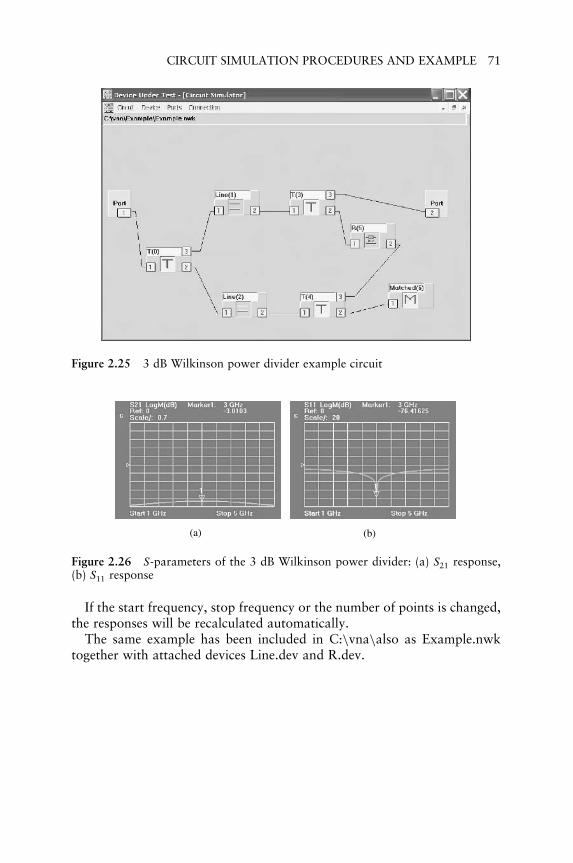
CIRCUIT SIMULATION PROCEDURES AND EXAMPLE 71
Figure 2.25 3 dB Wilkinson power divider example circuit
(a) (b)
Figure 2.26 S-parameters of the 3 dB Wilkinson power divider: (a) S21 response,(b) S11 response
If the start frequency, stop frequency or the number of points is changed,the responses will be recalculated automatically.
The same example has been included in C:\vna\also as Example.nwktogether with attached devices Line.dev and R.dev.


3Device Builders and Models
ABSTRACT
The Software VNA has 35 device builders, from which an unlimited numberof devices can be defined. The devices built can be used for simulationstudies either as a single DUT or as a part of a circuit to be assembled usingthe Circuit Simulator. In this chapter, these device builders are described indetail. The equations used for the modelling of devices are provided.
KEYWORDS
Microwave devices, Device modelling equations, Discrete components, Idealcomponents, Transmission lines, Active components, Transmission linediscontinuities, Coupled transmission lines, Lumped elements, Antennas,User-defined devices.
The Software VNA described in Chapter 2 has 35 device builders, whichare listed again in Table 3.1. An unlimited number of devices can bedefined using these device builders, which can then be used for simulationstudies either as a single DUT or as part of a circuit assembled using theCircuit Simulator. In this chapter, these device builders will be described indetail. A list of equations used for device modelling will be given. For theS-parameter measurements, the reference port impedance is always assumedto be Z0�ref = 50� or the reference port admittance to be Y0�ref =1/Z0�ref .In the case of one-port device, it is assumed that the DUT is connectedto Port 1 of the Software VNA, and Port 2 of the Software VNA is left
Software VNA and Microwave Network Design and Characterisation Zhipeng Wu© 2007 John Wiley & Sons, Ltd
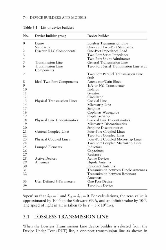
74 DEVICE BUILDERS AND MODELS
Table 3.1 List of device builders
No. Device builder group Device builder
0 Demo Lossless Transmission Line1 Standards One- and Two-Port Standards2 Discrete RLC Components One-Port Impedance Load3 Two-Port Series Impedance4 Two-Port Shunt Admittance5 Transmission Line General Transmission Line6 Transmission Line
ComponentsTwo-Port Serial Transmission Line Stub
7 Two-Port Parallel Transmission LineStub
8 Ideal Two-Port Components Attenuator/Gain Block9 1:N or N :1 Transformer10 Isolator11 Gyrator12 Circulator13 Physical Transmission Lines Coaxial Line14 Microstrip Line15 Stripline16 Coplanar Waveguide17 Coplanar Strip18 Physical Line Discontinuities Coaxial Line Discontinuities19 Microstrip Discontinuities20 Stripline Discontinuities21 General Coupled Lines Four-Port Coupled Lines22 Two-Port Coupled Lines23 Physical Coupled Lines Four-Port Coupled Microstrip Lines24 Two-Port Coupled Microstrip Lines25 Lumped Elements Inductors26 Capacitors27 Resistors28 Active Devices Active Devices29 Antennas Dipole Antenna30 Resonant Antenna31 Transmission between Dipole Antennas32 Transmission between Resonant
Antennas33 User-Defined S-Parameters One-Port Device34 Two-Port Device
‘open’ so that S22 = 1 and S12 = S21 = 0. For calculations, the zero value isapproximated by 10−30 in the Software VNA, and an infinite value by 1030.The speed of light in air is taken to be c = 3×10⁸m/s.
3.1 LOSSLESS TRANSMISSION LINE
When the Lossless Transmission Line device builder is selected from theDevice Under Test (DUT) list, a one-port transmission line as shown in

LOSSLESS TRANSMISSION LINE 75
Figure 3.1 Lossless Transmission Line: (a) One-Port option and (b) Two-Portoption
Figure 3.1(a) will be displayed. The characteristic impedance, propagationvelocity and length of the lossless transmission line can be assigned. Thetermination load can be selected to be a short-circuit load, an open-circuit

76 DEVICE BUILDERS AND MODELS
load, a load with RLC connected in parallel or a load with RLC connectedin series. The RLC values can be inputted. If a component does not exist,the corresponding input field can be either left blank or assigned an input ofNo. The ‘nonexisting’ component will be replaced by a short circuit acrossthe component in the series case and by an open circuit in the parallel case.The Software VNA will assign an appropriate ‘zero’ or ‘infinite’ value forthe component. If the option of Two-Port is selected, the two-port losslesstransmission line is as shown in Figure 3.1(b).
The S-parameter of the one-port lossless transmission line is given by
S11 = Zin −Z0�ref
Zin +Z0�ref� �3.1�
where
Zin = Z0ZL + jZ0 tan��L�
Z0 + jZL tan��L��3.2�
and
� = �
vp= 2�f
vp �3.3�
The load impedance ZL depends on the user’s choice, and
ZL =
⎧⎪⎪⎪⎪⎪⎪⎨⎪⎪⎪⎪⎪⎪⎩
0 short circuit� open circuit[R+ j
(�L− 1
�C
)]−1
RLC in parallel[R+ j
(�L− 1
�C
)]RLC in series
�3.4�
The S-parameters for the two-port lossless transmission line are given by
S� =
[j�Z2
0 −Z20�ref� sin��L� 2Z0Z0�ref
2Z0Z0�ref j�Z20 −Z2
0�ref� sin��L�
]2Z0Z0�ref cos��L�+ j�Z2
0 +Z20�ref� sin��L�
�3.5�
3.2 ONE- AND TWO-PORT STANDARDS
Figure 3.2 shows the display of the One- and Two-Port Standards. Thestandards include Short, Open, Matched Load or Thru. They are directlyconnected to the ports of the Software VNA with zero transmission line

ONE- AND TWO-PORT STANDARDS 77
Figure 3.2 One- and Two-Port Standards
lengths. The one-port standards are connected to Port 1 of the SoftwareVNA and the two-port standard to both Port 1 and Port 2 of theSoftware VNA.
The S-parameters for the standards are tabulated in Table 3.2.
Table 3.2 The S-parameters of one- and two-port standards
Standards S-parameters
Port 1: Short S� =[−1 0
0 1
]
Port 1: Open S� =[
1 00 1
]
Port 1: Matched Load S� =[
0 00 1
]
Thru S� =[
0 11 0
]
Note: Port 2 of the Software VNA is left open forone-port connection to Port 1

78 DEVICE BUILDERS AND MODELS
3.3 DISCRETE RLC COMPONENTS: ONE-PORTIMPEDANCE LOAD
Figure 3.3 shows the display of the Discrete RLC Components: One-PortImpedance Load device builder. The load consisting of both RLC in seriesand RLC in parallel is connected to Port 1 of the Software VNA with zerotransmission line length. All RLC values can be inputted. If a componentdoes not exist, the corresponding input field can be either left blank orassigned an input of No. The ‘nonexisting’ component will be replacedby a short circuit in the series case and by an open circuit in the parallelcase. The Software VNA will assign an appropriate ‘zero’ or ‘infinite’ valueaccordingly.
The S-parameter of the one-port impedance load is given by
S11 = ZL −Z0�ref
ZL +Z0�ref� �3.6�
where
ZL = Rs + j(
�Ls −1
�Cs
)+ Rp
1+ jRp
(�Cp − 1
�Lp
) �3.7�
The subscripts s and p represent the series and parallel components,respectively.
Figure 3.3 Discrete RLC Components: One-Port Impedance Load
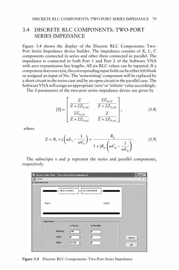
DISCRETE RLC COMPONENTS: TWO-PORT SERIES IMPEDANCE 79
3.4 DISCRETE RLC COMPONENTS: TWO-PORTSERIES IMPEDANCE
Figure 3.4 shows the display of the Discrete RLC Components: Two-Port Series Impedance device builder. The impedance consists of R, L, Ccomponents connected in series and other three connected in parallel. Theimpedance is connected to both Port 1 and Port 2 of the Software VNAwith zero transmission line lengths. All six RLC values can be inputted. If acomponentdoesnotexist, thecorresponding input fieldcanbeeither leftblankor assigned an input of No. The ‘nonexisting’ component will be replaced bya short circuit in the series case and by an open circuit in the parallel case. TheSoftware VNA will assign an appropriate ‘zero’ or ‘infinite’ value accordingly.
The S-parameters of the two-port series impedance device are given by
S� =
⎡⎢⎢⎢⎢⎣
Z
Z +2Z0�ref
2Z0�ref
Z +2Z0�ref
2Z0�ref
Z +2Z0�ref
Z
Z +2Z0�ref
⎤⎥⎥⎥⎥⎦ � �3.8�
where
Z = Rs + j(
�Ls −1
�Cs
)+ Rp
1+ jRp
(�Cp − 1
�Lp
) �3.9�
The subscripts s and p represent the series and parallel components,respectively.
Figure 3.4 Discrete RLC Components: Two-Port Series Impedance

80 DEVICE BUILDERS AND MODELS
3.5 DISCRETE RLC COMPONENTS: TWO-PORTSHUNT ADMITTANCE
Figure 3.5 shows the display of the discrete RLC components: Two-PortSingle Admittance device builder. The admittance consists of R, L, Ccomponents connected in series and other three connected in parallel. Theshunt admittance is connected to both ports of the Software VNA with zerotransmission line lengths. The RLC values can be inputted. If a componentdoes not exist, the corresponding input field can be either left blank orassigned an input of No. The ‘nonexisting’ component will be replacedby a short circuit in the series case and by an open circuit in the parallelcase. The Software VNA will assign an appropriate ‘zero’ or ‘infinite’ valueaccordingly.
The S-parameters of the two-port single admittance device aregiven by
S� =
⎡⎢⎢⎣
−YZ0�ref
2+YZ0�ref
22+YZ0�ref
22+YZ0�ref
−YZ0�ref
2+YZ0�ref
⎤⎥⎥⎦ � �3.10�
where
Y =
⎡⎢⎢⎢⎢⎣Rs + j
(�Ls −
1�Cs
)+ Rp
1+ jRp
(�Cp − 1
�Lp
)⎤⎥⎥⎥⎥⎦
−1
�3.11�
The subscripts s and p represent the series and parallel components,respectively.
Figure 3.5 Discrete RLC Components: Two-Port Shunt Admittance

GENERAL TRANSMISSION LINE 81
3.6 GENERAL TRANSMISSION LINE
Figure 3.6 shows the display of the General Transmission Line devicebuilder. Unlike the lossless transmission line in Section 3.1, the generaltransmission line can be lossy, i.e. the attenuation constant may havea finite nonzero value. The transmission line is a two-port device andis connected to both ports of the Software VNA. The transmission lineparameters including characteristic impedance, attenuation constant at1 GHz, frequency dependence of the attenuation constant, phase velocityw.r.t. the speed of light in air and length can be inputted.
The attenuation constant is usually frequency and geometry dependent.A value at 1 GHz needs to be obtained for a given transmission linegeometry. For a lossless transmission line, the attenuation constant is 0.For normal conductors, the attenuation constant due to conducting lossincreases proportionally to the square root of frequency. The frequencydependence factor of the attenuation constant is 0.5. For superconductors,the factor may be between 1 and 2. The factor may be 1 for attenuationdue to dielectric losses.
Both characteristic impedance and phase velocity of a transmission linedepend on its geometry and dielectric filling between the conductors. For apure TEM transmission line, the phase velocity is given by
vp = c√�r
� �3.12�
where c is the speed of light in air and �r the relative dielectric constant ofthe dielectric filling in the transmission line.
Figure 3.6 General Transmission Line

82 DEVICE BUILDERS AND MODELS
The S-parameters of the general transmission line are given by
S� =
[�Z2
0 −Z20�ref� sinh� L� 2Z0Z0�ref
2Z0Z0�ref �Z20 −Z2
0�ref� sinh� L�
]2Z0Z0�ref cosh� L�+ �Z2
0 +Z20�ref� sinh� L�
� �3.13�
where
= �+ j� with � = �
vp �3.14�
3.7 TRANSMISSION LINE COMPONENTS:TWO-PORT SERIAL TRANSMISSION LINESTUB
Figure 3.7 shows the display of the Transmission Line Components:Two-Port Serial Transmission Line Stub device builder. The stub isconnected to both ports of the Software VNA with zero transmissionline lengths. The transmission line parameters including characteristicimpedance, attenuation constant at 1 GHz, frequency dependence of theattenuation constant, phase velocity w.r.t. the speed of light in air andlength can be inputted in the same way as that in Section 3.6. Thetermination load can be chosen to be a short circuit, open circuit or50� load.
Figure 3.7 Transmission Line Components: Two-Port Serial Transmission LineStub

TRANSMISSION LINE COMPONENTS 83
The S-parameters of the serial transmission line stub with load impedanceZL are given by
S� =
⎡⎢⎢⎢⎣
Zin
Zin +2Z0�ref
2Z0�ref
Zin +2Z0�ref
2Z0�ref
Zin +2Z0�ref
Zin
Zin +2Z0�ref
⎤⎥⎥⎥⎦ � �3.15�
where
Zin = Z0ZL +Z0 tanh� L�
Z0 +ZL tanh� L��3.16�
with = � + j� and � = �/vp. For a short-circuit termination, ZL = 0�,and for an open-circuit termination, ZL = ��. The S-parameters of theserial transmission line stub can also be given by
S� =
⎡⎢⎢⎣
1+S11z
3−S11z
2�1−S11z�
3−S11z2�1−S11z�
3−S11z
1+S11z
3−S11z
⎤⎥⎥⎦ � �3.17�
where
S11z = S�TL�11 + S
�TL�12 S
�TL�21 �L
1−S�TL�22 �L
�3.18�
with S��TL� being the S-parameters of the transmission line section, i.e.
S��TL� =
[�Z2
0 −Z20�ref� sinh� L� 2Z0Z0�ref
2Z0Z0�ref �Z20 −Z2
0�ref� sinh� L�
]2Z0Z0�ref cosh� L�+ �Z2
0 +Z20�ref� sinh� L�
�3.19�
and
�L = ZL −Z0�ref
ZL +Z0�ref �3.20�
3.8 TRANSMISSION LINE COMPONENTS:TWO-PORT PARALLEL TRANSMISSION LINESTUB
Figure 3.8 shows the display of the Transmission Line Components:Two-Port Parallel Transmission Line Stub device builder. The stub isconnected to both ports of the Software VNA with zero transmission

84 DEVICE BUILDERS AND MODELS
Figure 3.8 Transmission Line Components: Two-Port Parallel Transmission LineStub
line lengths. The transmission line parameters including characteristicimpedance, attenuation constant at 1 GHz, frequency dependence of theattenuation constant, phase velocity w.r.t. the speed of light in air and lengthcan be inputted in the same way as that in Section 3.6. The terminationload can again be chosen to be a short circuit, open circuit or 50� load.
The S-parameters of the parallel transmission line stub with loadimpedance ZL are given by
S� =
⎡⎢⎢⎢⎢⎣
−YinZ0�ref
2+YinZ0�ref
22+YinZ0�ref
22+YinZ0�ref
−YinZ0�ref
2+YinZ0�ref
⎤⎥⎥⎥⎥⎦ � �3.21�
where
Yin =[Z0
ZL +Z0 tanh� L�
Z0 +ZL tanh� L�
]−1
�3.22�
with = �+ j� and � = �/vp.The S-parameters of the parallel transmission line stub can also be given by
S� =
⎡⎢⎢⎢⎢⎣
S11z −13+S11z
2�1+S11z�
3+S11z
2�1+S11z�
3+S11z
S11z −13+S11z
⎤⎥⎥⎥⎥⎦ � �3.23�

IDEAL TWO-PORT COMPONENTS 85
where
S11z = S�TL�11 + S
�TL�12 S
�TL�21 �L
1−S�TL�22 �L
�3.24�
with S��TL� being the S-parameters of the transmission line section, i.e.
S��TL� =
⎡⎢⎢⎣ �Z2
0 −Z20�ref� sinh� L� 2Z0Z0�ref
2Z0Z0�ref �Z20 −Z2
0�ref� sinh� L�
⎤⎥⎥⎦
2Z0Z0�ref cosh� L�+ �Z20 +Z2
0�ref� sinh� L��3.25�
and
�L = ZL −Z0�ref
ZL +Z0�ref �3.26�
3.9 IDEAL TWO-PORT COMPONENTS:ATTENUATOR/GAIN BLOCK
Figure 3.9 shows the display of the Ideal Two-Port Components:Attenuator/Gain Block device builder. The device is connected to both portsof the Software VNA with zero transmission line lengths. The value of
Figure 3.9 Ideal Two-Port Components: Attenuator/Gain Block

86 DEVICE BUILDERS AND MODELS
attenuation or gain in dB can be inputted. The S-parameters of the blockare
S� =[
0 eGdB/8686
eGdB/8686 0
]� �3.27�
where GdB is the gain in dB. If GdB is negative, the gain block becomes anattenuation block.
3.10 IDEAL TWO-PORT COMPONENTS: 1:N ANDN :1 TRANSFORMER
Figure 3.10 shows the display of the Ideal Two-Port Components: 1:N andN :1 Transformer device builder. The device is connected to both ports ofthe Software VNA with zero transmission line lengths. A selection of 1:N orN :1 transformation can be made, and the value of N which can be greateror less than 1 can be inputted. The S-parameters of the 1:N transformer are
S� =
⎡⎢⎢⎢⎢⎢⎢⎣
1−N 2
1+N 2
2N
1+N 2
2N
1+N 2
N 2 −11+N 2
⎤⎥⎥⎥⎥⎥⎥⎦
�3.28�
Figure 3.10 Ideal Two-Port Components: 1:N and N :1 Transformer

IDEAL TWO-PORT COMPONENTS: GYRATOR 87
and those of the N :1 transformer are
S� =
⎡⎢⎢⎢⎢⎢⎢⎣
N 2 −11+N 2
2N
1+N 2
2N
1+N 2
1−N 2
1+N 2
⎤⎥⎥⎥⎥⎥⎥⎦
�3.29�
3.11 IDEAL TWO-PORT COMPONENTS:ISOLATOR
Figure 3.11 shows the display of the Ideal Two-Port Components: Isolatordevice builder. The device is connected to both ports of the SoftwareVNA with zero transmission line lengths. The S-parameters of the idealisedisolator are
S� =[
0 01 0
] �3.30�
3.12 IDEAL TWO-PORT COMPONENTS:GYRATOR
Figure 3.12 shows the display of the Ideal Two-Port Components: Gyrator
Figure 3.11 Ideal Two-Port Components: Isolator

88 DEVICE BUILDERS AND MODELS
Figure 3.12 Ideal Two-Port Components: Gyrator
device builder. The device is connected to both ports of the SoftwareVNA with zero transmission line lengths. The S-parameters of the idealisedgyrator are
S� =[
0 1−1 0
] �3.31�
3.13 IDEAL TWO-PORT COMPONENTS:CIRCULATOR
Figure 3.13 shows the display of the Ideal Two-Port Components:Circulator device builder. The circulator is a three-port device. Any port ofthe circulator can be selected from the list to connect to Port 1 or Port 2 ofthe Software VNA. However, a port cannot be selected to connect to bothPort 1 and Port 2 simultaneously. When this happens, the Software VNAwould automatically select an alternative connection. When the selectionsare made, the remaining port is assumed to be terminated by a matched load.The S-parameters of the idealised circulator are
S� =⎡⎣0 0 1
1 0 00 1 0
⎤⎦ �3.32�

PHYSICAL TRANSMISSION LINES: COAXIAL LINE 89
Figure 3.13 Ideal Two-Port Components: Circulator
3.14 PHYSICAL TRANSMISSION LINES: COAXIALLINE
Figure 3.14 shows the display of the Physical Transmission Lines: CoaxialLine device builder. The coaxial line is a two-port device. The electricalparameters including the radii of inner and outer conductors, conductivity
Figure 3.14 Physical Transmission Lines: Coaxial Line

90 DEVICE BUILDERS AND MODELS
of the conductor with respect to that of copper, i.e. 58×108S/m, relativedielectric constant of the dielectric material and its loss tangent and lengthof the coaxial line can be inputted. The cut-off frequency of the structurefor TEM propagation will be calculated when either one of the dimensionsor the relative dielectric constant is changed.
The characteristic impedance of the coaxial line is given by (Pozar, 1990;Wadell, 1991)
Z0 = 60√�r
ln(
b
a
) �3.33�
The propagation constant of the coaxial line is
= �+ j�� �3.34�
where
� = Rs
4�
1Z0
(1a
+ 1b
)+ �
2c
√�r tan� and � = �
c
√�r �3.35�
with Rs =√��0/2� and c is the speed of light in air. The cut-off frequency
for TEM propagation is calculated by (Pozar, 1990; Wadell, 1991)
fcutoff = c
��a+b�√
�r �3.36�
The S-parameters of the coaxial line can be obtained using the aboveparameters and the equations for the general transmission line described inSection 3.6, i.e.
S� =
[�Z2
0 −Z20�ref� sinh� L� 2Z0Z0�ref
2Z0Z0�ref �Z20 −Z2
0�ref� sinh� L�
]2Z0Z0�ref cosh� L�+ �Z2
0 +Z20�ref� sinh� L�
�3.37�
3.15 PHYSICAL TRANSMISSION LINES:MICROSTRIP LINE
Figure 3.15 shows the display of the Physical Transmission Lines: MicrostripLine device builder. The microstrip line is a two-port device. The width andthickness of the strip and its conductivity w.r.t. that of copper, thickness ofthe dielectric substrate, relative dielectric constant and loss tangent of thesubstrate and length of the microstrip line can be inputted. The radiationloss of the microstrip line may be included in the modelling. The cut-offfrequency of the structure for quasi-TEM propagation will be calculated

PHYSICAL TRANSMISSION LINES: MICROSTRIP LINE 91
Figure 3.15 Physical Transmission Lines: Microstrip Line
when either one of the dimensions or the relative dielectric constant ischanged.
The characteristic impedance of the microstrip line is given by thefollowing equations (Bahl, 1989):
Z0 =
⎧⎪⎪⎨⎪⎪⎩
60√�re
ln(
8h
w′ +025w′
h
)for w/h < 1
120�√�re
[w′
h+1393+0667 ln
(w′
h+1444
)]−1
for w/h ≥ 1�
�3.38�where
w′
h=
⎧⎪⎪⎨⎪⎪⎩
w
h+ 125
�
t
h
(1+ ln
(4�w
t
))for
w
h<
12�
w
h+ 125
�
t
h
(1+ ln
(2h
t
))for
w
h≥ 1
2�
�3.39�
and the effective dielectric constant
�re = �r +12
+ �r −12
F �w/h�− �r −146
t
h
(w
h
)−1/2�3.40�

92 DEVICE BUILDERS AND MODELS
with
F �w/h� =
⎧⎪⎪⎨⎪⎪⎩
(1+ 12h
w
)−05
+004(1− w
h
)2for
w
h< 1(
1+ 12h
w
)−05
forw
h> 1
�3.41�
With the consideration of dispersion in the microstrip line, the frequency-dependent effective dielectric constant and characteristic impedance aregiven, respectively, by
�re� f � =(√
�r −√�re
1+4F −15+√
�re
)�3.42�
and
Z0� f � = Z0�re�f�−1�re −1
√�re
�re� f �� �3.43�
where
F = 4hf√
�r −1c
{05+
[1+2 ln
(1+ w
h
)]2}
�3.44�
with c = 3×10⁸ m/s.The attenuation constant � includes conducting, dielectric and radiation
losses, i.e.
� = �c +�d +�r �3.45�
with a unit of Neper/m. The attenuation constant �c is given by
�c =
⎧⎪⎪⎪⎨⎪⎪⎪⎩
01588Rs
hZ0
32− �w′/h�2
32+ �w′/h�2A for w/h < 1
070228×10−5 RsZ0�re
h
[w′
h+ 0667w′/h
w/h+1444
]A for w/h ≥ 1
�3.46�with
A =
⎧⎪⎪⎪⎨⎪⎪⎪⎩
1+ h
w′
[1+ 125t
�w+ 125
�ln(
4�w
t
)]for
w
h<
12�
1+ h
w′
[1− 125t
�h+ 125
�ln(
2h
t
)]for
w
h≥ 1
2�
�3.47�

PHYSICAL TRANSMISSION LINES: MICROSTRIP LINE 93
and
Rs =√
��0
2� �3.48�
The attenuation constant �d is given by
�d = �f
c
�r√�re� f �
�re� f �−1�r −1
tan� �3.49�
and �r by
�r = �f
cQr= �f
c
(480��hf/c�2R
√�re� f �
Z0
)�3.50�
with
R = �re� f �+1�re� f �
− ��re� f �−1�2
2�re� f �3/2ln
√�re� f �+1√�re� f �−1
�3.51�
The cut-off frequency for quasi-TEM propagation is estimated by (Wadell,1991)
fcutoff =
⎧⎪⎨⎪⎩
c
4h√
�r −1for �r > 2
c
4hfor �r ≤ 2
�3.52�
Using the above equations for the characteristic impedance and thepropagation constant
= �+ j� with � = 2�f
c
√�re� f �� �3.53�
the S-parameters of the microstrip line can be obtained using the equationsfor the general transmission line described in Section 3.6, i.e.
S� =
⎡⎣(Z2
0 −Z20�ref
)sinh� L� 2Z0Z0�ref
2Z0Z0�ref
(Z2
0 −Z20�ref
)sinh� L�
⎤⎦
2Z0Z0�ref cosh� L�+(Z2
0 +Z20�ref
)sinh� L�
�3.54�

94 DEVICE BUILDERS AND MODELS
3.16 PHYSICAL TRANSMISSION LINES: STRIPLINE
Figure 3.16 shows the display of the Physical Transmission Lines: Striplinedevice builder. The stripline is a two-port device. The width and thicknessof the strip and its conductivity w.r.t. that of copper, thickness of dielectricsubstrate, relative dielectric constant and loss tangent of the substrate andlength of the stripline can be inputted. The cut-off frequency of the structurefor TEM propagation will be calculated when either one of the dimensionsor the relative dielectric constant is changed.
The characteristic impedance of the stripline is given by the followingequations (Pozar, 1990; Wadell, 1991; Bahl, 1989; Howe, 1974):
Z0 = 30�√�r
b
we +0441b� �3.55�
where
we
b=⎧⎨⎩
w
bfor
w
b> 035
w
b−(035− w
b
)2for
w
b≤ 035
�3.56�
The attenuation constant � includes both conducting and dielectriclosses, i.e.
� = �c +�d �3.57�
Figure 3.16 Physical Transmission Lines: Stripline

PHYSICAL TRANSMISSION LINES: STRIPLINE 95
The attenuation constant �c is given by
�c =
⎧⎪⎪⎨⎪⎪⎩
27 ×10−3Rs�rZ0
30��b− t�A for
√�rZ0 < 120
016Rs
Z0bB for
√�rZ0 ≥ 120
� �3.58�
where
A = 1+ 2w
b− t+ 1
�
b+ t
b− tln(
2b− t
t
)�
B = 1+ b
�05w+07t�
(05+ 0414t
w+ 1
2�ln(
4�w
t
)) �3.59�
and
Rs =√
��0
2� �3.60�
The attenuation constant �d is given by
�d = �f
c
√�r tan�� �3.61�
where c is the speed of light in air. The cut-off frequency for TEMpropagation is estimated by (Wadell, 1991)
fcutoff = c
2w√
�r �3.62�
Using the above equations for the characteristic impedance and thepropagation constant given by
= �+ j� with � = 2�f
c
√�r� �3.63�
the S-parameters of the stripline can be obtained using the equations forthe general transmission line described in Section 3.6, i.e.
S� =
[�Z2
0 −Z20�ref� sinh� L� 2Z0Z0�ref
2Z0Z0�ref �Z20 −Z2
0�ref� sinh� L�
]2Z0Z0�ref cosh� L�+ �Z2
0 +Z20�ref� sinh� L�
�3.64�

96 DEVICE BUILDERS AND MODELS
3.17 PHYSICAL TRANSMISSION LINES:COPLANAR WAVEGUIDE
Figure 3.17 shows the display of the Physical Transmission Lines: CoplanarWaveguide device builder. The coplanar waveguide is a two-port device. Thewidth and thickness of the strip and its conductivity w.r.t. that of copper,gap between strips, thickness of dielectric substrate, relative dielectricconstant and loss tangent of the substrate and length of the coplanarwaveguide can be inputted. The radiation loss of the structure may beincluded in the modelling. The cut-off frequency of the structure for quasi-TEM propagation will be calculated when either one of the dimensions orthe relative dielectric constant is changed.
The characteristic impedance of the coplanar waveguide is given by(Gupta, Garg, Bahl and Bhartia, 1996)
Z0 = 30�√�re
K′�ke�
K�ke�� �3.65�
where K�ke� and K′�ke� are the complete elliptic integrals of the first kindand its complement, respectively, with argument ke given by
ke = s + �125t/��1+ ln�4�s/t��
s +2w− �125t/��1+ ln�4�s/t���3.66�
Figure 3.17 Physical Transmission Lines: Coplanar Waveguide

PHYSICAL TRANSMISSION LINES: COPLANAR WAVEGUIDE 97
and K′�ke� = K�√
1−k2e �. The effective relative dielectric constant �re is given
by
�re = 1+ �r −12
K�k2�
K′�k2�
K′�k1�
K�k1��3.67�
with
k1 = s
s +2wand k2 =
sinh(�s
4h
)sinh
(��s +2w�
4h
) �3.68�
The elliptic functions can be approximated by (Gupta, Garg, Bahl andBhartia, 1996)
K�k� =
⎧⎪⎪⎪⎪⎨⎪⎪⎪⎪⎩
�
2�1+2�k/8�+9�k/8�2
+50�k/8�3 +30625�k/8�4 +· · · � for 0 ≤ k < 007
p+ �p−1��k′2/4�+9�p−7/6��k′4/64�+25�p−137/30��k′6/256�+· · · for 0707 ≤ k ≤ 1
�3.69�
with
k′ =√
1−k2 and p = ln�4/k′� �3.70�
or
K�k�
K′�k�=
⎧⎪⎪⎨⎪⎪⎩
�
ln2�1+√k′�/�1−√k′��
for 0 ≤ k < 007
ln2�1+√k�/�1−√k��
�for 0707 ≤ k ≤ 1
�3.71�
The attenuation constant � includes conducting, dielectric and radiationlosses, i.e.
� = �c +�d +�r �3.72�
The attenuation constant �c is given by
�c = Rs√
�re
480�K′�k1��1−k21�
{2s
[� + ln
(4�s�1−k2
1�
t�1+k21�
)]
+ 2s +2w
[� + ln
(4��s +2w��1−k2
1�
t�1+k21�
)]} (3.73)

98 DEVICE BUILDERS AND MODELS
with
Rs =√
��0
2� �3.74�
The attenuation constant �d is given by
�d = �f
c
�r√�re
�re −1�r −1
tan�� �3.75�
where c is the speed of light in air, and the attenuation constant �r is givenby
�r = 2(�
2
)5 �1−�re/�r�2√
�re/�r
�s +2w�2
K�k1�K′�k1�
(f√
�r
c
)3
�3.76�
The cut-off frequency for quasi-TEM propagation is estimated by(Wadell, 1991)
fcutoff = c
�s +2w�√
��r +1�/2 �3.77�
Using the above equations for the characteristic impedance and thepropagation constant
= �+ j� with � = 2�f
c
√�re� �3.78�
the S-parameters of the coplanar waveguide can be obtained using theequations for the general transmission line described in Section 3.6, i.e.
S� =
[�Z2
0 −Z20�ref� sinh� L� 2Z0Z0�ref
2Z0Z0�ref �Z20 −Z2
0�ref� sinh� L�
]2Z0Z0�ref cosh� L�+ �Z2
0 +Z20�ref� sinh� L�
�3.79�
3.18 PHYSICAL TRANSMISSION LINES:COPLANAR STRIPS
Figure 3.18 shows the display of the Physical Transmission Lines: CoplanarStrips device builder. The coplanar strip is a two-port device. The widthand thickness of the strips and their conductivity w.r.t. that of copper,gap between strips, thickness of dielectric substrate, relative dielectricconstant and loss tangent of the substrate and length of the coplanarstrips can be inputted. The radiation loss of the structure may be includedin the modelling. The cut-off frequency of the structure for quasi-TEM

PHYSICAL TRANSMISSION LINES: COPLANAR STRIPS 99
Figure 3.18 Physical Transmission Lines: Coplanar Strips
propagation will be calculated when either one of the dimensions or therelative dielectric constant is changed.
The characteristic impedance of the coplanar strips is given by (Gupta,Garg, Bahl and Bhartia, 1996)
Z0 = 120�√�re
K�k1�
K′�k1�� �3.80�
where K�k1� and K′�k1� have been given in Section 3.17. The argument k1is defined as
k1 = s
s +2w �3.81�
The effective relative dielectric constant �re is given by
�re = 1+ �r −12
K�k2�
K′�k2�
K′�k1�
K�k1��3.82�
with
k2 =sinh
(�s
4h
)sinh
(��s +2w�
4h
) �3.83�
The attenuation constant � includes conducting, dielectric and radiationlosses, i.e.
� = �c +�d +�r �3.84�

100 DEVICE BUILDERS AND MODELS
The attenuation constant �c is given by,
�c = Rs√
�re
480�K′�k1��1−k21�
{2s
[� + ln
(4�s�1−k2
1�
t�1+k21�
)]
+ 2s +2w
[� + ln
(4��s +2w��1−k2
1�
t�1+k21�
)]} (3.85)
with
Rs =√
��0
2� �3.86�
The attenuation constant �d is given by
�d = �f
c
�r√�re
�re −1�r −1
tan�� �3.87�
where c is the speed of light in air, and the attenuation constant �r is givenby
�r = �3−√8�(�
2
)2√
�re
�r
(�r −12�r
)2 w2
K�k1�K′�k1�
(f√
�r
c
)3
�3.88�
The cut-off frequency for quasi-TEM propagation is estimated by(Wadell, 1991)
fcutoff = c
�s +2w�√
��r +1�/2 �3.89�
Using the above equations for the characteristic impedance and thepropagation constant given by
= �+ j� with � = 2�f
c
√�re� �3.90�
the S-parameters of the coplanar strip can be obtained using the equationsfor the general transmission line described in Section 3.6, i.e.
S� =
[�Z2
0 −Z20�ref� sinh� L� 2Z0Z0�ref
2Z0Z0�ref �Z20 −Z2
0�ref� sinh� L�
]2Z0Z0�ref cosh� L�+ �Z2
0 +Z20�ref� sinh� L�
�3.91�

PHYSICAL LINE DISCONTINUITIES 101
3.19 PHYSICAL LINE DISCONTINUITIES:COAXIAL LINE DISCONTINUITIES
Figure 3.19(a)–(c) shows the coaxial step, gap and open-end discontinuities,respectively, together with their equivalent circuits. The models of thesediscontinuities are described below.
3.19.1 Step Discontinuity
The step discontinuity can be represented by a shunt capacitance Ceq. Theshunt capacitance is modelled by (Wadell, 1991)
Ceq = ��r1 +�r2��r1Cd2 + ��r1 +�r2��r1avCd1� �3.92�
where Cd1 is the capacitance for the inner step and Cd2 the capacitance forthe outer step. They are given by
Cd1 = �0
�
[�2
1 +1�1
ln1+�1
1−�1−2 ln
4�1
1−�21
]+111×10−13 �1−�1� ��1 −1� �F/m��
Cd2 = �0
�
[�2
2 +1�2
ln1+�2
1−�2−2 ln
4�2
1−�22
]+412×10−13 �1−�2� ��2 −14� �F/m��
�3.93�with
r1av = r0 + r1
2� �2 = r2 − r1av
r3 − r1avand �2 = r3
r1av
r3av = r3 + r2
2� �1 = r3av − r1
r3av − r0and �1 = r3av
r0
�3.94�
It should be noted that the factor �1−�2� instead of �08−�2� in Equation(3.93) is used in Cd2 so that the formulas are applicable to the range 001 ≤� ≤ 1 and 1 ≤ � ≤ 60 for both outer and inner steps.
The S-parameters of the step discontinuity can then be obtained usingthe equations for a two-port shunt admittance device described in Section3.5, i.e.
S� =
⎡⎢⎢⎣
−YZ0�ref
2+YZ0�ref
22+YZ0�ref
22+YZ0�ref
−YZ0�ref
2+YZ0�ref
⎤⎥⎥⎦ �3.95�
with
Y = j�Ceq �3.96�

102 DEVICE BUILDERS AND MODELS
3.19.2 Gap Discontinuity
The gap discontinuity can be modelled as a series capacitor. The equivalentseries capacitance Ceq is given by
Figure 3.19 Physical Line Discontinuities: Coaxial Line Discontinuities: (a) step,(b) gap and (c) open end

PHYSICAL LINE DISCONTINUITIES 103
Figure 3.19 (Continued)
Ceq = �0�r�a2
s �3.97�
The S-parameters of the gap discontinuity can then be obtained using theequations for a two-port series impedance device described in Section 3.4,i.e.
S� =
⎡⎢⎢⎣
Z
Z +2Z0�ref
2Z0�ref
Z +2Z0�ref2Z0�ref
Z +2Z0�ref
Z
Z +2Z0�ref
⎤⎥⎥⎦ �3.98�
with
Z = 1j�Ceq
�3.99�
3.19.3 Open-End Discontinuity
The open-end discontinuity can be modelled as an equivalent admittance(Misra et al., 1990; Marcuvitz, 1951), which is given by Y = G+ jB with
G = 23
(k0
√�rout
2
)4 (b2 −a2
)2 Y0√
�rout
ln(b/
a)√
�rin
�3.100�

104 DEVICE BUILDERS AND MODELS
and
B = 2Y0k0�rout
� ln(b/
a)√
�rin
[(a2 +b2
)1/2� −2 �a+b�
]� �3.101�
where Y0 =√�0/�0 = 1/120�. These formulas are valid for k0
√�rb ≤ 1. If
the external medium is of low loss with loss tangent tan �, the G and Bvalues can be approximated to
G′ = G�1− j tan��5/2 = G
(1− j
52
tan�
)� B′ = B�1− j tan�� �3.102�
so that
Y = G′ + jB′ = �G+B tan��+ j(
B− 52
G tan�
) �3.103�
The S-parameter of the open-end discontinuity can then be obtained usingthe equations for a one-port terminated load described in Section 3.3, i.e.
S11 = ZL −Z0�ref
ZL +Z0�ref�3.104�
with
ZL = 1/Y �3.105�
3.20 PHYSICAL LINE DISCONTINUITIES:MICROSTRIP LINE DISCONTINUITIES
Figure 3.20(a)–(e) shows, respectively, the microstrip step, gap, bend, slitand open-end discontinuities together with their equivalent circuits. Themodels of these discontinuities are described below.
3.20.1 Step Discontinuity
The step discontinuity can be represented by series inductance L1,shunt capacitance Cs and series inductance L2 (Gupta, Garg, Bahl and

PHYSICAL LINE DISCONTINUITIES 105
(a)
L1 L2
Cs
R2I2 C2
C11 C11C12
C12
L12L12
R1 R1
L11 L11
(b)
L1 L2
Cs
(c)
Figure 3.20 Physical Line Discontinuities: Microstrip Line Discontinuities: (a) step,(b) gap, (c) bend, (d) slit and (e) open end

106 DEVICE BUILDERS AND MODELS
(d)
LN
C1
C2
L
R
(e)
Figure 3.20 (Continued)
Bhartia, 1996), where
L1 =(
Z0m1√
�re1
Z0m1√
�re1 +Z0m2√
�re2
)Ls� L2 =
(Z0m2
√�re2
Z0m1√
�re1 +Z0m2√
�re2
)Ls�
Cs = 1370h
√�re1
Z0m1
(1− w2
w1
)(�re1 +03
�re1 −0258
)(w1
/h+0264
w1
/h+08
)�pF�
(3.106)

PHYSICAL LINE DISCONTINUITIES 107
and
Ls = 987h
(1− Z0m1
Z0m2
√�re1
�re2
)2
�nH� �3.107�
with Z0m and �re values calculated using the microstrip line equations inSection 3.15 for conductor thickness t = 0.
The S-parameters of the step discontinuity can then be obtained usingthe equations for a ‘T’ impedance network in Table 1.8, Section 1.5, i.e.
S� =
[−Z2
0�ref + �Z1 −Z2�Z0�ref +Z1Z2 +Z2Z3 +Z3Z1 2Z0�refZ3
2Z0�refZ3 −Z20�ref + �Z2 −Z1�Z0�ref +Z1Z2 +Z2Z3 +Z3Z1
]
Z20�ref + �Z1 +Z2 +2Z3�Z0�ref +Z1Z2 +Z2Z3 +Z3Z1
�3.108�
with
Z1 = j�L1� Z2 = j�L2 and Z3 = 1/�j�Cs� �3.109�
3.20.2 Gap Discontinuity
The model used to describe the gap discontinuity is that by Alexopolousand Wu (1994). The R, L and C values of the equivalent circuit shown inFigure 3.20(b) are given by
C11 × 25Z0
h=[1125 tanh
(1358
w
h
)−0315
]tanh
[(00262+0184
h
w
)
+(0217 +00619 ln
w
h
) S
h
]�pF���
C12 × 25Z0
h=[6832 tanh
(00109
w
h
)+0910
]tanh
[(1411+0314
h
w
)
+(
S
h
)1248+0360 tan−1 w/h]
�pF���
L11 × 25hZ0
=[0134+00436 ln
h
w
]exp
[−1×
(3656+0246
h
w
)(
S
h
)1739+0390 ln w/h]
�nH/���

108 DEVICE BUILDERS AND MODELS
L12 × 25hZ0
=[0008285 tanh
(05665
w
h
)+00103
]
+[01827 +000715 ln
w
h
]
exp
[−1×
(5207 +1283 tanh
(1656
h
w
))(S
h
)0542+0873 tan−1 w/h]
�nH/���
R1
/Z0 =1024 tanh
(2025
w
h
)tanh
[(001584+00187
h
w
)S
h
+(01246+00394sinh
(w
h
))]�
C2 × 25Z0
h=[01776+005104 ln
(w
h
)] h
S+[0574+03615
h
w
+1156 ln(w
h
)]sech
(23345
S
h
)�pF���
L2 × 25hZ0
=[
000228+ 00873752w
/h+ cosh
(w/
h)]
sinh(
23345S
h
)�nH/��� �nH/��
R2
/Z0 =
[−178+0749
w
h
] S
h+[1196−0971 ln
(w
h
)]sinh
(23345
S
h
)�
(3.110)where Z0 is the characteristic impedance of the microstrip line calculatedusing the equations presented in Section 3.15.
The S-parameters of the gap discontinuity can then be obtained using theequations for a ‘�’ admittance network in Table 1.8, Section 1.5, i.e.
S� =
[Y 2
0�ref − �Y1 −Y2�Y0�ref − �Y1Y2 +Y2Y3 +Y3Y1� 2Y0�refY3
2Y0�refY3 Y 20�ref − �Y2 −Y1�Y0�ref − �Y1Y2 +Y2Y3 +Y3Y1�
]
Y 20�ref + �Y1 +Y2 +2Y3�Y0�ref +Y1Y2 +Y2Y3 +Y3Y1
(3.111)

PHYSICAL LINE DISCONTINUITIES 109
with
Y1 =Y2 =(
j�L11 + 1j�C11
)−1
+(
R1 + j�L12 + 1j�C12
)−1
and
Y3 =(
R2 + j�L2 + 1j�C2
)−1
(3.112)
3.20.3 Bend Discontinuity
The 90� bend discontinuity can also be represented by series inductance L1,shunt capacitance Cs and series inductance L2 (Wadell, 1991), where
L1 = L2 = Ls
2= Ls = 50h
(4
√w
h−421
)�nH��
Cs =
⎧⎪⎪⎪⎪⎨⎪⎪⎪⎪⎩
⎡⎢⎣ �14�r +125�
(w/
h)− �183�r −225�√
w/
h+ 002�r
w/
h
⎤⎥⎦w �pF� if w < h
[�95�r +125�
(w
h
)+52�r +7
]w �pF� if w ≥ h
(3.113)
These formulas are accurate to within 5% for 25 ≤ �r ≤ 150 and 01 ≤w/
h ≤ 50.The S-parameters of the bend discontinuity can then be obtained using
the equations for a ‘T’ impedance network in Table 1.8, Section 1.5, i.e.
S� =
[−Z2
0�ref + �Z1 −Z2�Z0�ref +Z1Z2 +Z2Z3 +Z3Z1 2Z0�refZ3
2Z0�refZ3 −Z20�ref + �Z2 −Z1�Z0�ref +Z1Z2 +Z2Z3 +Z3Z1
]
Z20�ref + �Z1 +Z2 +2Z3�Z0�ref +Z1Z2 +Z2Z3 +Z3Z1
(3.114)
with
Z1 = j�L1� Z2 = j�L2 and Z3 = 1/�j�Cs� �3.115�

110 DEVICE BUILDERS AND MODELS
3.20.4 Slit Discontinuity
The slit discontinuity can be modelled by series inductance LN given by(Gupta, Garg, Bahl and Bhartia, 1996)
LN = 2000h
(1− Z0m
Z′0m
√�re
�′re
)2
�nH�� �3.116�
where Z0m and �re are the characteristic impedance and the effective relativedielectric constant of the microstrip line with width w, respectively, andZ′
0m and �′re are the values for the microstrip line with width (w–b).
The S-parameters of the slit discontinuity can then be obtained using theequations for a two-port single series impedance described in Section 3.4, i.e.
S� =
⎡⎢⎢⎢⎣
Z
Z +2Z0�ref
2Z0�ref
Z +2Z0�ref
2Z0�ref
Z +2Z0�ref
Z
Z +2Z0�ref
⎤⎥⎥⎥⎦ �3.117�
with
Z = j�LN �3.118�
3.20.5 Open-End Discontinuity
The open-end discontinuity can be modelled as an equivalent admittancegiven by (Alexopolous and Wu, 1994)
Y = j�C1 +(
R+ j�L+ 1j�C2
)−1
�3.119�
with
C1 × 25Z0
h= 1125 tanh
(1358
w
h
)−0315 �pF���
C2 × 25Z0
h= 6832 tanh
(00109
w
h
)+0910 �pF���
L× 25hZ0
= 0008285 tanh(05665
w
h
)+00103 �pF���

PHYSICAL LINE DISCONTINUITIES 111
R/
Z0 = 1024 tanh(2025
w
h
)� �3.120�
where Z0 is the characteristic impedance of the microstrip line calculatedusing the equations in Section 3.15.
The S-parameter of the open-end discontinuity can then be obtained usingthe equations for a one-port terminated load described in Section 3.3, i.e.
S11 = ZL −Z0�ref
ZL +Z0�ref�3.121�
with
ZL = 1/Y �3.122�
3.21 PHYSICAL LINE DISCONTINUITIES:STRIPLINE DISCONTINUITIES
Figure 3.21(a)–(d) shows, respectively, the stripline step, gap, bend andopen-end discontinuities together with their equivalent circuits. The modelsof these discontinuities are described below.
3.21.1 Step Discontinuity
The step discontinuity can be modelled simply by series inductance Ls givenby (Gupta, Garg and Chadha, 1981)
Ls =√
�rw′1Z01
�cln
(1
sin(�w′
2
/2w′
1
))
� �3.123�
where
Z01 = Z0�w = w1�� w′1 = w′�w = w1�� w′
2 = w′�w = w2� �3.124�
with (Pozar, 1990; Howe, 1974)
Z0 = 30�h√�r �we +0441b�
�

112 DEVICE BUILDERS AND MODELS
(a)
L
BB
BA BA
(b)
Figure 3.21 Physical Line Discontinuities: Stripline Discontinuities: (a) step, (b)gap, (c) bend and (d) open end

PHYSICAL LINE DISCONTINUITIES 113
(c)
(d)
La La
Cb
Cshunt
Figure 3.21 (Continued)

114 DEVICE BUILDERS AND MODELS
we ={
w if w > 035h
w−h(035− w
h
)2if w ≤ 035h
�
w=
⎧⎪⎨⎪⎩
hK �k�
K′ �k�if w < 05h
w−h(035− w
h
)2if w > 05h
�
k = tanh(�w
2h
) �3.125�
The S-parameters of the step discontinuity can then be obtained using theequations for a two-port single series impedance described in Section 3.4, i.e.
S� =
⎡⎢⎢⎢⎣
Z
Z +2Z0�ref
2Z0�ref
Z +2Z0�ref
2Z0�ref
Z +2Z0�ref
Z
Z +2Z0�ref
⎤⎥⎥⎥⎦ �3.126�
with
Z = j�Ls �3.127�
3.21.2 Gap Discontinuity
The gap discontinuity can be modelled by a ‘�’ network of three capacitors(Gupta, Garg and Chadha, 1981), as shown in Figure 3.21(b). Thesusceptance values of these three capacitors normalised to the characteristicadmittance of the stripline are, respectively,
�C1
Yo= B1 = 1+Ba cot
(�S/
2)
cot(�S/
2)−Ba
�
�C12
Yo= B12 = 1
2
⎛⎝1+
(2Bb +Ba
)cot
(�S/
2)
cot(�S/
2)−(2Bb +Ba
) −B1
⎞⎠ � �3.128�
where
Ba = −2b
�ln cosh
(�S/
2b)� Bb = b
�ln coth
(�S/
2b) �3.129�

PHYSICAL LINE DISCONTINUITIES 115
The S-parameters of the gap discontinuity can then be obtained using theequations for a ‘�’ admittance network in Table 1.8, Section 1.5, i.e.
S� =
[Y 2
0�ref − �Y1 −Y2�Y0�ref − �Y1Y2 +Y2Y3 +Y3Y1� 2Y0�refY3
2Y0�refY3 Y 20�ref − �Y2 −Y1�Y0�ref − �Y1Y2 +Y2Y3 +Y3Y1�
]
Y 20�ref + �Y1 +Y2 +2Y3�Y0�ref +Y1Y2 +Y2Y3 +Y3Y1
(3.130)
with
Y1 = Y2 = j�C1 and Y3 = j�C12 �3.131�
3.21.3 Bend Discontinuity
The 90� bend discontinuity can be modelled by series inductance L1, shuntcapacitance Cs and series inductance L2 = L1 (Gupta, Garg and Chadha,1981). Their normalised reactance values to the characteristic impedanceare given by
�L1
Z0= �L2
Z0= Xa = w′
�1756+4�w′/��2��
−1�CsZ0
= Xb = w′
�00725−0159��/w′�2�� �3.132�
with
w′ =
⎧⎪⎨⎪⎩
hK �k�
K′ �k�if w < 05h
w+ 2h
�ln 2 if w > 05h
and k = tanh(�w
2h
) �3.133�
The S-parameters of the bend discontinuity can then be obtained usingthe equations for a ‘T’ impedance network in Table 1.8, Section 1.5, i.e.
S� =
[−Z2
0�ref + �Z1 −Z2�Z0�ref +Z1Z2 +Z2Z3 +Z3Z1 2Z0�refZ3
2Z0�refZ3 −Z20�ref + �Z2 −Z1�Z0�ref +Z1Z2 +Z2Z3 +Z3Z1
]
Z20�ref + �Z1 +Z2 +2Z3�Z0�ref +Z1Z2 +Z2Z3 +Z3Z1
�3.134�
with
Z1 = j�L1� Z2 = j�L2 and Z3 = 1/�j�Cs� �3.135�

116 DEVICE BUILDERS AND MODELS
3.21.4 Open-End Discontinuity
The open end discontinuity can be modelled as an equivalent shunt capacitorof capacitance (Gupta, Garg and Chadha, 1981)
Cshunt =√
�r�l
cZ0� �3.136�
where Z0 is the characteristic impedance of the strip line and
��l = tan−1
[�+2W
4�+2Wtan ����
]� � = h
ln 2�
� � = 2�
�and � = �0√
�r
(3.137)
The S-parameter of the open-end discontinuity can then be obtained usingthe equations for a one-port terminated load described in Section 3.3, i.e.
S11 = ZL −Z0�ref
ZL +Z0�ref�3.138�
with
ZL = 1/�j�Cshunt� �3.139�
3.22 GENERAL COUPLED LINES: FOUR-PORTCOUPLED LINES
Figure 3.22 shows the display of the General Coupled Lines: Four-PortCoupled Lines device builder. The coupled line can be modelled using theeven–odd mode analysis (Pozar, 1990; Napoli and Hughes, 1970), whichleads to the S-parameters for the four-port device:
S� =
⎡⎢⎢⎣
S11 S21 S31 S41
S21 S11 S41 S31
S31 S41 S11 S21
S41 S31 S21 S11
⎤⎥⎥⎦
(3.140)
For a lossless coupled line,
S1131
= �e
2
(1−
(1−�2
e
)�ej2�eL −�2
e �
)± �o
2
(1−
(1−�2
o
)ej�oL
�ej2�oL −�2o�
)and
S2141
=( (
1−�2e
)ej�eL
2 �ej2�eL −�2e �
)±( (
1−�2o
)ej�oL
2 �ej2�oL −�2o�
)� (3.141)

GENERAL COUPLED LINES: TWO-PORT COUPLED LINES 117
Input
Coupled Isolated43
21 Thru
Figure 3.22 General Coupled Lines: Four-Port Coupled Lines
where
�e = −(1−Z0e
/Z0
)(1+Z0e
/Z0
) � �o = −(1−Z0o
/Z0
)(1+Z0o
/Z0
) � �3.142�
Z0e is the characteristic impedance of the even mode, Z0o the characteristicimpedance of the odd mode (Z0o < Z0e�, �e the phase constant of the evenmode and �o the phase constant of the odd mode (�o > �e�, and Z0 = Z0�ref .
If the coupled line is not lossless, the parameters j�e and j�o in the aboveequations are replaced, respectively, by
e = �e + j�e and o = �o + j�o �3.143�
3.23 GENERAL COUPLED LINES: TWO-PORTCOUPLED LINES
Figure 3.23 shows the display of the General Coupled Lines: Two-PortCoupled Lines device builder. Port 1 of the device is connected to Port 1of the VNA, and Port 4 to Port 2 of the VNA. Ports 2 and 3 of the devicecan be terminated by a short-circuit or open-circuit load with a reflectioncoefficient of �2 = �3 = −1 or �2 = �3 = 1. Since⎡
⎢⎢⎣b1
b2
b3
b4
⎤⎥⎥⎦=
⎡⎢⎢⎣
S11 S21 S31 S41
S21 S11 S41 S31
S31 S41 S11 S21
S41 S31 S21 S11
⎤⎥⎥⎦⎡⎢⎢⎣
a1
a2
a3
a4
⎤⎥⎥⎦ �3.144�

118 DEVICE BUILDERS AND MODELS
1 2
3 4
r2
r3
Figure 3.23 General Coupled Lines: Two-Port Coupled Lines
and
[b1b4
]=[
S11 S41S41 S11
][a1a4
]+[
S21 S31S31 S21
][�2 00 �3
][1−�2S11 −�3S41
−�2S41 1−�3S11
]−1
[S21 S31
S31 S21
][a1
a4
]�
[b1
b4
]=[
S′11 S′
41S′
41 S′11
][a1
a4
]=[
S′′11 S′′
12S′′
21 S′′22
][a1
a4
]� �3.145�
the new two-port S-parameters are
[S′′
11 S′′12
S′′21 S′′
22
]=[
S11 S41
S41 S11
]+[
S21 S31
S31 S21
][�2 00 �3
][1−�2S11 −�3S41
−�2S41 1−�3S11
]−1
[S21 S31
S31 S21
]�
(3.146)
where S11, S21, S31 and S41 are given in Section 3.22.

PHYSICAL COUPLED LINES 119
3.24 PHYSICAL COUPLED LINES: FOUR-PORTCOUPLED MICROSTRIP LINES
Figure 3.24 shows the display of the Physical Coupled Lines: Four-PortCoupled Microstrip Lines device builder. The coupled line can also bemodelled using the even–odd mode analysis.
The effective relative dielectric constant of the even mode is given by(Gupta, Garg, Bahl and Bhartia, 1996)
�ere �0� = �r +1
2+ �r −1
2
(1+ 10
�
)−aebe
�
� = u(20+g2
)10+g2
+ge−g�
ae = 1+ 149
ln
[�4 + (�/52
)2
�4 +0432
]+ 1
187ln[1+
( �
181
)3]
�
be = 0564(
�r −09�r +3
)0053
�3.147�
Figure 3.24 Physical Coupled Lines: Four-Port Coupled Microstrip Lines

120 DEVICE BUILDERS AND MODELS
This equation has an error of 0.7% for 01 ≤ u ≤ 10, 01 ≤ g ≤ 10 and1 ≤ �r ≤ 18, where u = w
/h and g = S
/h.
The effective relative dielectric constant of the odd mode is given by
�ore�0� = �re�0�+ �05��r +1�−�re�0�+ao�e
−co�gdo �� �3.148�
where �re �0� is the effective relative dielectric constant of a single microstripline,
ao = 07287��re�0�−05��r +1���1− e−0179u��
bo = 0747�r
015+�r�
co = bo − �bo −0207�e−0414u�
do = 0593+0694e−0562u �3.149�
The characteristic impedances of the even and odd modes are,respectively,
Z0e = Z0
√�re�0�
/�e
re�0�
1−Q4
√�re�0��Z0
/377�
and Z0o = Z0
√�re�0�
/�o
re�0�
1−Q10
√�re�0��Z0
/377�
�
(3.150)
where Z0 is the characteristic impedance of a single microstrip linecalculated using the equations in Section 3.15, and
Q1 = 088695u0194�
Q2 = 1+07519g +0189g231�
Q3 = 01975+[
166+(
84g
)6]−0387
+ 1241
ln
[g10
1+ (g/34)10
]�
Q4 = 2Q1
Q2
1uQ3e−g + �2− e−g�u−Q3
�
Q5 = 1974+114 ln[1+ 0638
g +0517g243
]�
Q6 = 02305+ 12813
ln[
g10
1+ �g/58�10
]+ 1
51ln�1+0598g1154��

PHYSICAL COUPLED LINES 121
Q7 = 10+190g2
1+823g3�
Q8 = e−65+095 ln�g�+�g/015�5��
Q9 = ln�Q7��Q8 +1/
165��
Q10 = Q4 − Q5
Q2eQ6 ln�u�
/uQ9 � (3.151)
The attenuation constant due to the conductor loss can be calculated usingthe Incremental Inductance Rule (Pozar, 1990). The attenuation constantsdue to the conductor loss for the even and odd modes are, respectively,
�ec =∑
�
Rs
240�Z0e
� �√
�oreZ0e�
��� �o
c =∑�
Rs
240�Z0o
� �√
�oreZ0o�
��� �3.152�
where Rs =√��0/2� is the surface resistance of the microstrip line, and �
represents a dimensional parameter of the microstrip coupled line.The attenuation constants due to dielectric losses for the even and odd
modes, respectively, are given by
�e�od = �r√
�e�ore
�e�ore −1�r −1
tan�
�0�Neper/m� �3.153�
The radiation loss of the odd mode is negligible. The attenuation constantof the even mode due to radiation loss is given by
�er = �f
cQr= �f
c
(480��hf/c�2R
√�e
re
Z0e
) �3.154�
with
R = �ere +1�e
re
− ��ere −1�2
2�e3/2re
ln√
�ere +1√
�ere −1
�3.155�
Hence the coupled microstrip line has the following parameters:
e = �e + j�e and o = �o + j�o� �3.156�
where
�e = �ec +�e
d +�er� �o = �o
c +�od� �e = 2�f
c
√�e
re and �o = 2�f
c
√�o
re
(3.157)

122 DEVICE BUILDERS AND MODELS
The S-parameters of the four-port coupled microstrip line are therefore
S� =
⎡⎢⎢⎣
S11 S21 S31 S41
S21 S11 S41 S31
S31 S41 S11 S21
S41 S31 S21 S11
⎤⎥⎥⎦ �3.158�
with
S1131
= �e
2
(1−
(1−�2
e
)�e2 eL −�2
e �
)± �o
2
(1−
(1−�2
o
)e eL
�e2 eL −�2o�
)and
S2141
=( (
1−�2e
)e eL
2 �e2 eL −�2e �
)±( (
1−�2o
)e eL
2 �e2 eL −�2o�
)�
(3.159)
where
�e = −(1−Z0e
/Z0
)(1+Z0e
/Z0
) � �o = −(1−Z0o
/Z0
)(1+Z0o
/Z0
) and Z0 = Z0�ref �3.160�
3.25 PHYSICAL COUPLED LINES: TWO-PORTCOUPLED MICROSTRIP LINES
Figure 3.25 shows the display of the Physical Coupled Lines: Two-PortCoupled Microstrip Lines device builder. Port 1 of the device is connected
Figure 3.25 Physical Coupled Lines: Two-Port Coupled Microstrip Lines

LUMPED ELEMENTS: INDUCTORS 123
to Port 1 of the VNA, and Port 4 to Port 2 of the VNA. Ports 2 and3 of the device can be terminated by a short-circuit or open-circuit loadwith a reflection coefficient of �2 = �3 = −1 or �2 = �3 = 1. As shown inSection 3.23, the S-parameters of the terminated coupled microstrip line are
[S′′
11 S′′12
S′′21 S′′
22
]=[
S11 S41
S41 S11
]+[
S21 S31
S31 S21
][�2 00 �3
][1−�2S11 −�3S41
−�2S41 1−�3S11
]−1 [S21 S31
S31 S21
]�
(3.161)
where S11, S21, S31 and S41 are given in Section 3.24.
3.26 LUMPED ELEMENTS: INDUCTORS
Figure 3.26(a)–(c) shows circular coil, circular spiral and single turn lumpedinductor device builders and their equivalent circuits, respectively. Theselumped elements models are described below.
3.26.1 Circular Coil
The circular coil can be modelled as an inductor L in series with a resistorR and in parallel with a capacitor C (Wadell, 1991). The overall impedanceof the coil is
Z = �R+ j�L��1/j�C�
�R+ j�L�+ �1/j�C� �3.162�
The inductance L is
L =
⎛⎜⎜⎝
�0n2�a2
b
[f1
(4a2
b2
)− 4
3�
2a
b
]b ≥ 2a
�0n2a2
{[ln(
8a
b
)− 1
2
]f1
(b2
4a2
)+ f2
(b2
4a2
)}b < 2a
� �3.163�
where
f1�x� = 1+0383901x+0017108x2
1+0258952xand
f2�x� = 0093842x+0002029x2 −0000801x3 (3.164)

124 DEVICE BUILDERS AND MODELS
with 0 ≤ x ≤ 10. The resistance R is
R =
⎧⎪⎪⎨⎪⎪⎩
Rs
2�aw�2�an� = Rsan
aw��� if �s < aw
16
�2�an�
�a2w
��� if �s > aw
� �3.165�
(a)
(b)
C
C
R
R
L
L
Figure 3.26 Lumped Elements: Inductors: (a) circular coil, (b) circular spiral and(c) single turn inductor

LUMPED ELEMENTS: INDUCTORS 125
(c)
C
R L
Figure 3.26 (Continued)
where Rs is the surface resistance of the coil, �s the skin depth and aw = d/2.The stray capacitance C is given by (Medhurst, 1947)
C = 200aH �pF�� �3.166a�
where
H = 01126b
2a+008+ 027√
b/
2a �3.166b�
The S-parameters of the circular coil in two-port connection can thenbe obtained using the equations for a two-port single series impedancedescribed in Section 3.4, i.e.
S� =
⎡⎢⎢⎣
Z
Z +2Z0�ref
2Z0�ref
Z +2Z0�ref2Z0�ref
Z +2Z0�ref
Z
Z +2Z0�ref
⎤⎥⎥⎦ �3.167�
3.26.2 Circular Spiral
The circular spiral lumped inductor can be modelled in the same equivalentcircuit as the circular coil (Wadell, 1991; Gupta, Garg and Chadha, 1981).

126 DEVICE BUILDERS AND MODELS
However, the inductance is given by
L = n2a2
8a+11coi�nH�� �3.168�
where a = �ro + ri�/2, coi = ro − ri which are in mils or
amil =(
1000254
)amm = 106ameter
254� coi�mil =
(1000254
)coi�mm = 106coi�meter
254
�3.169�The stray capacitance is given by
C = 0035 �2r0mm�+006 �pF� �3.170�
and the resistance R by
R =
⎧⎪⎨⎪⎩
Rs2� �05 �ro + ri�� n
2 �w+ t�= Rsan
awif �s <
12
wt
w+ t1�
2� �05 �ro + ri� n�
wtif �s >
12
wt
w+ t
� �3.171�
where Rs is the surface resistance of the coil and �s the skin depth.The S-parameters of the circular spiral in two-port connection are then
given by
S� =
⎡⎢⎢⎣
Z
Z +2Z0�ref
2Z0�ref
Z +2Z0�ref2Z0�ref
Z +2Z0�ref
Z
Z +2Z0�ref
⎤⎥⎥⎦ � �3.172�
where
Z = �R+ j�L�(1/
j�C)
�R+ j�L�+ (1/j�C) �3.173�
3.26.3 Single Turn Inductor
The single turn inductor can be modelled as an inductor L in series with aresistor R (Wadell, 1991). The inductance value is given by
L = 002339[�S1 +S2� ln
(2S1S2
w+ t
)−S1 ln �S1 +g�−S2 ln �S2 +g�
]
+001016[2g − S1 +S2
2+0447 �w+ t�
]��H�� (3.174)

LUMPED ELEMENTS: CAPACITORS 127
where
g =√
S21 +S2
2 �3.175�
and S1 and S2 are in inches which can be converted from millimetre ormetre using
S1�2 = S1�2mm
254= S1�2m ×103
254inch �3.176�
The resistance R is given by
R =
⎧⎪⎪⎨⎪⎪⎩
Rs2 �S1 +S2�
2 �w+ t�if �s <
12
wt
w+ t
1�
2�S1+S2�
wtotherwise
�3.177�
The S-parameters of the single turn inductor in two-port connection arethen given by
S� =
⎡⎢⎢⎢⎣
Z
Z +2Z0�ref
2Z0�ref
Z +2Z0�ref
2Z0�ref
Z +2Z0�ref
Z
Z +2Z0�ref
⎤⎥⎥⎥⎦ � �3.178�
where
Z = R+ j�L �3.179�
3.27 LUMPED ELEMENTS: CAPACITORS
Figure 3.27(a) and (b) shows, respectively, the thin film and interdigitallumped capacitor device builders and their equivalent circuits. Theparameters of the equivalent circuits are described below.
3.27.1 Thin Film Capacitor
The thin film capacitor is modelled as a capacitor with capacitance (Wadell,1991)
C = �r�0
h
[(l+ 4h ln 2
�
)(W + 4h ln 2
�
)]�F� �3.180�

128 DEVICE BUILDERS AND MODELS
Figure 3.27 Lumped Elements: Capacitors: (a) thin film capacitor and (b)interdigital capacitor

LUMPED ELEMENTS: RESISTOR 129
Hence the S-parameters of the thin film capacitor in two-port connectionare given by
S� =
⎡⎢⎢⎢⎣
Z
Z +2Z0�ref
2Z0�ref
Z +2Z0�ref
2Z0�ref
Z +2Z0�ref
Z
Z +2Z0�ref
⎤⎥⎥⎥⎦ � �3.181�
where
Z = 1/�j�C� �3.182�
3.27.2 Interdigital Capacitor
The capacitance of the interdigital capacitor is given by (Gupta, Garg andChadha, 1981)
C = l ��r +1� �N −3�A1 +A2� �pF�� �3.183�
where N is the total number of fingers,A1 = 0225pF/inch� A2 = 0252pF/inch and l is the length in inch.
Hence the S-parameters of the interdigital capacitor in two-portconnection are given by
S� =
⎡⎢⎢⎢⎣
Z
Z +2Z0�ref
2Z0�ref
Z +2Z0�ref
2Z0�ref
Z +2Z0�ref
Z
Z +2Z0�ref
⎤⎥⎥⎥⎦ � �3.184�
where
Z = 1/�j�C� �3.185�
3.28 LUMPED ELEMENTS: RESISTOR
Figure 3.28 shows the display of the Lumped Elements: Resistor devicebuilder. The resistance of the resistor is given by
R =
⎧⎪⎪⎨⎪⎪⎩
RsLtotal
2 �W + t�if 2�s < t
Ltotal
�Wtotherwise
� �3.186�
where Ltotal is the total meander line length, Rs the surface resistance of thecoil and �s the skin depth.

130 DEVICE BUILDERS AND MODELS
Figure 3.28 Lumped Elements: Resistor
3.29 ACTIVE DEVICES
Figure 3.29(a)–(d) shows the Active Devices device builders. The activedevice can be defined as a voltage-controlled voltage source, voltage-controlled current source, current-controlled voltage source, current-controlled current source. The S-parameters of these devices are, respectively(Dobrowolski, 1991)
S�V→V =[
1 02k −1
]� S�V→I =
[1 0
−2Z0g 1
]� S�I→V =
[ −1 02R/
Z0 −1
]�
S�I→I =[ −1 0−2b −1
]
(3.187)
3.30 ANTENNAS: DIPOLE ANTENNA
Figure 3.30 shows the display of the Antennas: Dipole Antenna devicebuilder. In terms of circuit, the antenna can be modelled as load impedancegiven by (Jordan, 1950; Kraus, 1989)
Rin �b� = 30
sin2 (b/2) 2 �1+ cosb� Si �b�− cosbS1 �2b� −2sinbSi �b�+ sinbSi �2b��
= 30
sin2�b/2�A�b��

ANTENNAS: DIPOLE ANTENNA 131
Figure 3.29 Active Devices: (a) voltage-controlled voltage source, (b) voltage-controlled current source, (c) current-controlled voltage source and (d) current-controlled current source

132 DEVICE BUILDERS AND MODELS
Figure 3.29 (Continued)
Xin�b� = −30
sin2 (b/2) {�sinb� ln
(H/
�a2)+ sinb − +2Ci �b�−Ci �2b��
− cosb 2Si �b�−Si �2b��−2Si �b�� = −30
sin2 (b/2) [�sinb� ln
(L2
2ba2
)+B �b�
]�
(3.188)

ANTENNAS: DIPOLE ANTENNA 133
Figure 3.30 Antennas: Dipole Antenna
where
A�b� = 2 �1+ cosb� Si �b�− cosbS1 �2b�−2sinbSi �b�+ sinbSi �2b� �
B �b� = sinb − +2Ci �b�−Ci �2b��− cosb 2Si �b�−Si �2b��−2Si �b� �
b = 2�H� H = L/
2� � = 2�
�= 2�f
c�
S1 �x� =x∫
0
1− cos�
�d� =
(x2
2 ·2! − x4
4 ·4! + x6
6 ·6! − · · ·+ · · ·)
= x2
4for x < 06�
S1�x� ≈ 1957 +008b−01sin�b� for x > 6�
Si�x� =x∫
0
sin�
�d� =
(x− x3
3!3 + x5
5!5 −· · ·)
={
x x < 05�
2− cosx
xx >> 1 �
Ci�x� = lnx+05772157−S1�x� =x∫
0
cos�
�d� =
{0577 + lnx for x < 02
sinx
xfor x >> 1
�3.189�

134 DEVICE BUILDERS AND MODELS
Table 3.3 A�b� and B�b� expansion coefficients
A �b� B �b� Term
−17297360e−05 79728378e−07 b10
78565342e−04 −26679835e−05 b9
−14319319e−02 43777030e−04 b8
13680252e−01 −48503360e−03 b7
−73924374e−01 36901743e−02 b6
22557770e+00 −16801097e−01 b5
−37426332e+00 38081304e−01 b4
38275498e+00 −54009365e−01 b3
−48368367e+00 21550133e+00 b2
56086056e+00 −49904193e+00 b1
−28144596e−01 −20374065e−01 b0
The calculation using the series expansion is very slow except for b < 0.6or b > 6. For 06 < b < 6, A�b� and B�b� are obtained by curve-fitting. Thecoefficients for b0 to b10 are given in the Table 3.3 for both A�b� and B�b�.
The S-parameter of the dipole antenna can then be obtained using theequations for a one-port terminated load described in Section 3.3, i.e.
S11 = ZL −Z0�ref
ZL +Z0�ref�3.190�
with
ZL = Zin = Rin + jXin �3.191�
3.31 ANTENNAS: RESONANT ANTENNA
Figure 3.31 shows the display of the Antennas: Resonant Antenna devicebuilder. This model applies to a resonance type of antenna near the resonancefrequency. The input admittance of the resonant antenna is defined as
Yin == 1R
+ j(
�C − 1�L
)= 1
R+ jQ0R
(f/
f0 − f0
/f)� �3.192�
where Q0 is the unloaded Q-factor and f0 the resonance frequency.The S-parameter of the resonant antenna is then given by
S11 = ZL −Z0�ref
ZL +Z0�ref�3.193�
with
ZL = Y −1in �3.194�

ANTENNAS: TRANSMISSION BETWEEN DIPOLE ANTENNAS 135
Figure 3.31 Antennas: Resonant Antenna
3.32 ANTENNAS: TRANSMISSION BETWEENDIPOLE ANTENNAS
Figure 3.32 shows the display of the Antennas: Transmission betweenDipole Antennas device builder. The reflection coefficients are given by
S11 = S22 = Zin −Z0�ref
Zin +Z0�ref� �3.195�
where Zin = Rin + jXin are calculated using the formulas in Section 3.30.Using the Radar Range Equation, the transmission coefficients can beobtained to be (Bryant, 1988)
S21 = S12 = S21 e−j�2�f /c�r � �3.196�
where
S21 =(1−S112
)1/2 (1−S222
)1/2164
(c
4�fr
) �3.197�
The gain of the dipole antenna is taken to be 1.64.

136 DEVICE BUILDERS AND MODELS
Figure 3.32 Antennas: Transmission between Dipole Antennas
3.33 ANTENNAS: TRANSMISSION BETWEENRESONANT ANTENNAS
Figure 3.33 shows the display of the Antennas: Transmission betweenResonant Antennas device builder. The reflection coefficients are given by
S11 = S22 = 1/
Yin −Z0�ref
1/
Yin −Z0�ref
= 1−Z0�refYin
1+Z0�refYin�3.198�
where Yin = �1/R�[1+ jQ0
(f/
f0 − f0
/f)]
as defined in Section 3.32. Thetransmission coefficients are given by
S21 = S21 e−j�2�f/c�r � �3.199�
where
S21 =(1−S112
)1/2 (1−S222
)1/2√GtGr
(c
4�fr
)=(1−S112
)G
(c
4�fr
)
(3.200)
The gain is taken to be G for both antennas.

USER-DEFINED S-PARAMETERS: ONE-PORT DEVICE 137
Figure 3.33 Antennas: Transmission between Resonant Antennas
3.34 USER-DEFINED S-PARAMETERS: ONE-PORTDEVICE
Figure 3.34 shows the display of the User-Defined S-Parameters: One-PortDevice builder. The user-defined S11 parameters at different frequencies inthe range between f1 and fM can be inputted, where the value of M is 51.These may include the measured S11 parameters or those of active devices.The Software VNA calculates the S-parameters of the device at differentfrequencies using the linear interpolation
S11�i �f � = S11�i+1f − fi
fi+1 − fi
+S11�i
fi+1 − f
fi+1 − fi
�3.201�
so that
S11 �f � =
⎧⎪⎪⎨⎪⎪⎩
M−1∑i=1
S11�i �f �U �fi+1� fi� if f1 ≤ f ≤ fM
S11�1 if f ≤ f1
S11�M if f > fM
� �3.202�
where
U �fi+1� fi� ={
1 if fi < f ≤ fi+1
0 �3.203�
In addition to the manual input, the one-port S-parameter saved usingthe SaveData function of the Software VNA for a simulated network or

138 DEVICE BUILDERS AND MODELS
S1 S2 S3 S4 Sm
i i + 1
Figure 3.34 User-Defined S-Parameters: One-Port Device
circuit can be imported into the device builder to form a new device byclicking on the Import button. In this case, only 51 frequency points areselected from the saved data from the first point to the last point with equalfrequency spacing.
3.35 USER-DEFINED S-PARAMETERS: TWO-PORTDEVICE
Figure 3.35 shows the display of the User-Defined S-Parameters: Two-Port Device builder. The user can define all four S-parameters at differentfrequencies in the range between f1 and fM , where the value of M is 51.These may include the measured S-parameters or those of active devices.The Software VNA calculates the S-parameters of the device at differentfrequencies using the linear interpolation
Si �f � = Si+1f − fi
fi+1 − fi
+Si
fi+1 − f
fi+1 − fi
�3.204�
so that
S �f � =
⎧⎪⎪⎨⎪⎪⎩
M−1∑i=1
Si �f �U �fi+1� fi� if f1 ≤ f ≤ fM
S1 if f ≤ f1
SM if f > fM
� �3.205�

REFERENCES 139
S1S2 S3
S4 Sm
i i + 1
Figure 3.35 User-Defined S-Parameters: Two-Port Device
where
U �fi+1� fi� ={
1 if fi < f ≤ fi+1
0 �3.206�
and S represents each of the four S-parameters.In addition to the manual input, the two-port S-parameters saved using
the SaveData function of the Software VNA for a simulated network orcircuit can be imported into the device builder to form a new device byclicking on the Import button. In this case, only 51 frequency points areselected from the saved data from the first point to the last point with equalfrequency spacing.
REFERENCES
Alexopolous, N.G. and Wu, S. (1994) ‘Frequency-independent equivalent circuit modelfor microstrip open-end and gap discontinuities’. IEEE Transactions on MicrowaveTheory and Techniques, MTT-42 (7), 1268–72.
Bahl, I.J. (1989) Transmission lines, in Handbook of Microwave and OpticalComponents – Vol. 1: Microwave Passive and Antenna Components (ed. K. Chang),John Wiley & Sons, Ltd, New York, pp. 1–59.
Bryant, G.H. (1988) Principles of Microwave Measurements, IEE, London.Dobrowolski, J.A. (1991) Introduction to Computer Methods for Microwave Circuit
Analysis and Design, Artech House, Boston.Gupta, K.C., Garg, R. and Chadha, R. (1981) Computer Aided Design of Microwave
Circuits, Artech House, Norwood.

140 DEVICE BUILDERS AND MODELS
Gupta, K.C., Garg, R., Bahl, I. and Bhartia, P. (1996) Microstrip Lines and Slotlines,2nd edn, Artech House, Norwood.
Howe, H., Jr (1974) Stripline Circuit Design, Artech House, Dedham, MA.Jordan, E.C. (1950)Electromagnetic Waves and Radiating Systems, Prentice-Hall,
Englewood Cliffs, NJ.Kraus, J.D. (1989) Antennas, McGraw-Hill, New York.Marcuvitz, N. (1951) Waveguide Handbook, McGraw-Hill, New York.Medhurst, R.G. (1947) ‘H.F. resistance and self-capacitance of single-layer solenoids’.
Wireless Engineer, 80–92.Misra, D. et al. (1990) ‘Noninvasive electrical characterisation of materials at microwave
frequencies using an open-ended coaxial line: test of an improved calibrationtechnique’. IEEE Transactions on Microwave Theory and Techniques, MTT-38, 8–14.
Napoli, L.S. and Hughes, J.J. (1970) ‘Characteristics of coupled microstrip lines’. RCAReview, 479–98.
Pozar, D.M. (1990) Microwave Engineering, Addison-Wesley, New York.Wadell, B.C. (1991) Transmission Line Design Handbook, Artech House, Norwood,
1991.

4Design of Microwave Circuits
ABSTRACT
The Circuit Simulator in the Software VNA can be used to simulatemicrowave circuits assembled with the devices built using the device buildersin the software package. In this chapter, the design principles of a numberof commonly used microwave circuits impedance matching, impedancetransformers, microwave resonators, power dividers, couplers, hybrid rings,phase shifters, filters and amplifier design are described.
KEYWORDS
Microwave circuits, Impedance matching, Impedance transformers,Microwave resonators, Power dividers, Couplers, Hybrid rings, Phaseshifters, Filters, Amplifier design
The Circuit Simulator in the Software VNA can be used to simulatemicrowave circuits assembled with the devices built using the device buildersdescribed in Chapter 3. In this chapter, the design principles of a numberof commonly used microwave circuits are described. Examples of circuitsimulation using the Circuit Simulator will be presented in Chapter 5.
4.1 IMPEDANCE MATCHING
4.1.1 Impedance Matching Using a Discrete Element
The use of a quarter-wave transformer and a discrete element is thesimplest technique for impedance matching. The diagram of this impedancematching technique is shown in Figure 4.1. The load impedance is denotedas ZL = RL + jXL and admittance YL = 1/ZL = GL + jBL. If the load
Software VNA and Microwave Network Design and Characterisation Zhipeng Wu© 2007 John Wiley & Sons, Ltd

142 DESIGN OF MICROWAVE CIRCUITS
C ZLZ0
λ /4
Figure 4.1 Impedance matching using a discrete element
impedance is inductive, a discrete capacitor of capacitance C is connectedin parallel to the load impedance so that the overall impedance is resistiveat the required matching frequency f0. This leads to
C = − B
2�f0�4.1�
and the resultant resistance of 1/GL. A quarter-wave transformer is thenused to transform the resultant resistance to the source impedance ofZs = 50�. The characteristic impedance of the quarter-wave transformeris required to be
Z0 =√50/GL� �4.2�
If the load impedance is capacitive, an inductor can be used to replace thecapacitor. The load impedance can then be matched to the source impedancein a similar way. A disadvantage of this matching technique is that it requiresthe design and fabrication of different quarter-wave transformers if the loadimpedance is changed.
4.1.2 Single Stub Matching
The principle of single stub matching is to transform the load impedanceZL = RL + jXL using a section of transmission line of length L1 and standardcharacteristic impedance, e.g. Z0 = 50� to an admittance of Yin1 = 0�02+ jB(Collin, 1966). An open- or short-circuited stub of the same characteristicimpedance but length L2 is then connected in parallel to the equivalentadmittance with an input admittance of Yin2 = −jB to cancel the reactive partof Yin1. This results in the impedance matching to the source impedance ofZs = 50�. The diagram of the single stub matching is shown in Figure 4.2.The required lengths L1 and L2 can be calculated using
L1
�={
12�
tan−1 t if t ≥ 01
2�
(� + tan−1 t
)if t < 0
�4.3�

IMPEDANCE MATCHING 143
ZL
Z0 = 50 Ω
Z0 = 50 Ω
Yin1Yin2
L2
Z0 = 50 Ω L1
Figure 4.2 Single stub matching
and
L2
�= +1
2�tan−1
(1
Z0B
)�4.4�
for a short-circuited stub where
t = tan ��d� =XL ±
√RL
[�Z0 −RL�2 +X2
L
]/Z0
RL −Z0�RL �= Z0� �4.5�
and
B = R2Lt − �Z0 −XLt� �XL +Z0t�
Z0
[R2
L + �XL +Z0t�2] � �4.6�
There are two possible solutions of L1, and consequently L2. Thelength L2 may also be different if an open-circuited stub is used. Thedisadvantage of the single stub matching technique is that it requiresdifferent transmission line lengths when the load impedance is changed.
4.1.3 Double Stub Matching
The double stub matching technique may overcome the disadvantage ofthe single stub matching (Collin, 1966; Pozar, 1990). In this technique,two stubs are used. The first stub is connected in parallel with the loadimpedance ZL = RL + jXL or admittance YL = 1/ZL = GL + jBL. A fixedlength of transmission line, d, is used between the load and the second stub.The diagram of this matching technique is shown in Figure 4.3.
The length of the transmission line between two stubs is chosen so that
0 ≤ GL ≤ Y01+ t2
2t2= Y0
sin2 �d �4.7�

144 DESIGN OF MICROWAVE CIRCUITS
Short or open stubs
Y2
jB2
jB1
d
Y1YL = GL + jBL
Figure 4.3 Double stub matching
where t = tan ��d� and Y0 is the characteristic admittance of the transmissionline. In practice, d is usually chosen to be �/8 or 3�/8. The length of thefirst stub is required to be
ls1
�=⎧⎨⎩
−12�
tan−1(
Y0B1
)for short-circuited stub
12�
tan−1(
B1Y0
)for open-circuited stub
�4.8�
in which
B1 = −BL + Y0 ±√�1+ t2�GLY0 −G2Lt2
t� �4.9�
Similarly the length of the second stub is required to be
ls2
�=⎧⎨⎩
−12�
tan−1(
Y0B2
)for short-circuited stub
12�
tan−1(
B2Y0
)for open-circuited stub
�4.10�
where
B2 = ±Y0
√Y0GL�1+ t2�−G2
Lt2 +GLY0
GLt� �4.11�
The input admittance after the first stub is
Y1 = GL + j �BL +B1� �4.12�
and that before the second stub is
Y2 = Y0GL + j �BL +B1 +Y0t�
Y0 + jt �GL + jBL + jB1�= Y0 − jB2� �4.13�
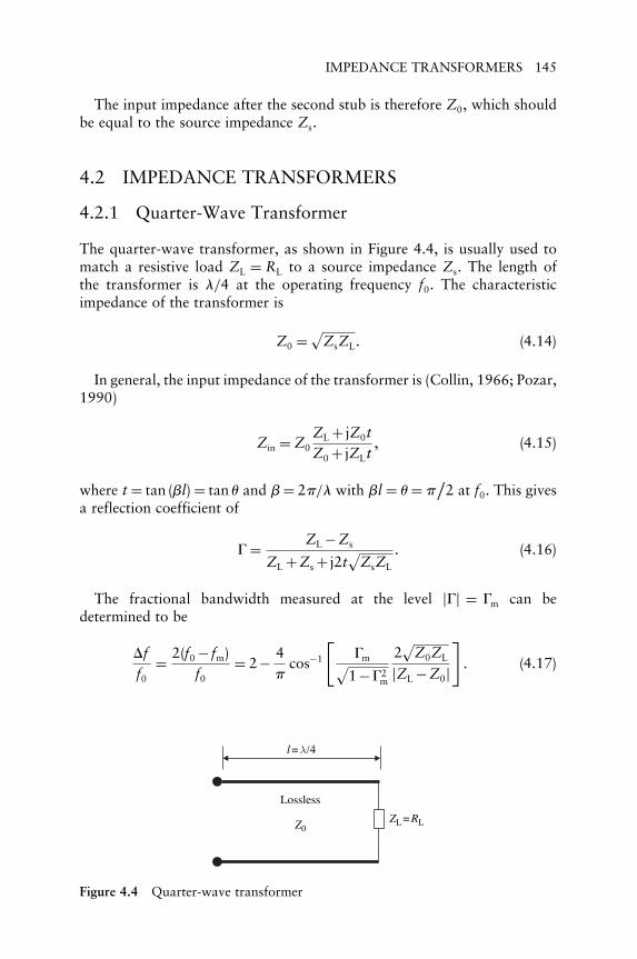
IMPEDANCE TRANSFORMERS 145
The input impedance after the second stub is therefore Z0, which shouldbe equal to the source impedance Zs.
4.2 IMPEDANCE TRANSFORMERS
4.2.1 Quarter-Wave Transformer
The quarter-wave transformer, as shown in Figure 4.4, is usually used tomatch a resistive load ZL = RL to a source impedance Zs. The length ofthe transformer is �/4 at the operating frequency f0. The characteristicimpedance of the transformer is
Z0 =√ZsZL� �4.14�
In general, the input impedance of the transformer is (Collin, 1966; Pozar,1990)
Zin = Z0ZL + jZ0t
Z0 + jZLt �4.15�
where t = tan ��l� = tan and � = 2�/� with �l = = �/
2 at f0. This givesa reflection coefficient of
� = ZL −Zs
ZL +Zs + j2t√
ZsZL
� �4.16�
The fractional bandwidth measured at the level �� � = �m can bedetermined to be
�f
f0= 2�f0 − fm�
f0= 2− 4
�cos−1
[�m√
1−�2m
2√
Z0ZL
�ZL −Z0�
]� �4.17�
Lossless
ZL = RLZ0
l = λ /4
Figure 4.4 Quarter-wave transformer

146 DESIGN OF MICROWAVE CIRCUITS
4.2.2 Chebyshev Multisection Matching Transformer
The Chebyshev multisection matching transformer, as shown in Figure 4.5,is also used to match a resistive load ZL = RL to a source impedance Zs
(Collin, 1966; Pozar, 1990). Each transmission line section is �/4 long atthe operating frequency f0. The characteristic impedance of each line sectionis to be determined.
In general, the reflection coefficient of the terminated multisectiontransmission line system is given by
��� =
⎧⎪⎪⎨⎪⎪⎩
2e−jN �0 cosN +�1 cos �N −2� +· · ·+�n cos �N −2n�+· · ·+ 1
2�N/2
]for even N
2e−jN �0 cosN +�1 cos �N −2� +· · ·+�n cos �N −2n�+· · ·+��N−1�/2 cos
]for odd N
�4.18�where
�0 = Z1 −Z0
Z1 +Z0 �n = Zn+1 −Zn
Zn+1 +Zn
�N = ZL −ZN
ZL +ZN
�4.19�
and Z0 = Zs is the source impedance, Zn the characteristic impedance ofthe nth section. With the assumption that the transformer is symmetrical,the following equalities can be established:
�0 = �N �1 = �N−1 �2 = �N−2 and so on� �4.20�
The characteristic impedance of each transmission line section can bedetermined when �n values are assigned. Using the Chebyshev polynomialswhich can be expressed as
Z0 Z1 Z2 ΖN ZL
θ θ θ θ
|Γ|
Γm
f0
(Δθ)
0 θm π/2 π – θmθ = βl
Figure 4.5 Chebyshev multisection matching transformer

IMPEDANCE TRANSFORMERS 147
TN �x� = cos(N cos−1 x
)for �x� < 1 and TN �x�
= cosh(N cosh−1
x)
for �x� > 1 (4.21)
with �TN �x = ±1� � = 1 the reflection coefficient can be written as
� �� = �me−jNTN �secm cos� �4.22�
where N is the number of sections, a frequency-dependent quantity whichis related to the electric length of the line section, �m the maximum allowablereflectioncoefficient in thematchedbandwhichoccursatm and�−m where
secm = cosh[
1N
cosh−1(
1�m
∣∣∣∣ZL −Z0
ZL +Z0
∣∣∣∣)]
� �4.23�
At the central operating frequency f0, = �/2 and the length of the linesection is �/4. The fractional bandwidth of the Chebyshev multisectionmatching transformer is given by
�f
f0= 2− 4m
�� �4.24�
In the case that N = 2,
� �� = �me−j2T2 �secm cos� = e−j2�m
[sec2 m �1+ cos2�−1
]= e−j2�m
[sec2 m cos2 + (sec2 m −1
)]= 2e−j2
[�0 cos2 + �1
2
](4.25)
and
secm = cosh[
12
cosh−1(
1�m
∣∣∣∣ZL −Z0
ZL +Z0
∣∣∣∣)]
� �4.26�
Hence
�0 = �2 = 12
�m sec2 m and �1 = �m
(sec2 m −1
)�4.27�
from which Z1 and Z2 can be calculated.In the case that N = 3,
� �� = �me−j3T3 �secm cos�
= e−j3�m
[sec3 m cos3 +3sec3 m cos −3secm cos
]= e−j3�m
[sec3 m cos3 +3secm
(sec2 m −1
)cos
]= 2e−j3 �0 cos3 +�1 cos� (4.28)

148 DESIGN OF MICROWAVE CIRCUITS
and
secm = cosh[
13
cosh−1(
1�m
∣∣∣∣ZL −Z0
ZL +Z0
∣∣∣∣)]
� �4.29�
Hence
�0 = �3 = 12
�m sec3 m and �1 = �2 = 12
�m ·3secm�sec2 m −1� �4.30�
from which Z1, Z2 and Z3 can be calculated.In the case that N = 4,
� �� = �mT4�secm cos� = 2[�0 cos4 +�1 cos�2�+ 1
2�2
]
= �m sec4 m cos4 +4sec4 m cos2 +3sec4 m −4sec2 m cos2
+1−4sec2 m�
= �m sec4 m cos4 +4sec2 m�sec2 m −1� cos2 +1+3sec4 m
−4sec2 m� (4.31)
so that
�0 = �4 = 12
�m sec4 m �1 = �3 = 2�m sec2 m�sec2 m −1� and
�2 = �m�1+3sec4 m −4sec2 m��
(4.32)
The characteristic impedance of each line section, Z1, Z2, Z3 and Z4, canthen be calculated.
4.2.3 Corporate Feeds
Figure 4.6(a) and (b) shows the two basic configurations of corporate feedswhich are commonly used in antenna arrays. The antenna array can bematched to a 50� feed line by the successive application of the basiccorporate feed.
In the first configuration, the 50� arms and feed line can be of anylength. The impedance transformer is, however, �/4 long. It transformsthe resultant impedance of two 50� impedances connected in parallel tothe impedance of the feed line, i.e. 50�, so that the transformer has acharacteristic impedance of
Z0 = √25×50 = 35�4�� �4.33�

MICROWAVE RESONATORS 149
λ /4Z0
Z0 Z0
50 Ω 50 Ω
50 Ω 50 Ω
50 Ω
50 Ω
λ /2
(a) (b)
Figure 4.6 Corporate feed: (a) configuration 1 and (b) configuration 2
In the second configuration, the 50� arms and feed line can beof any length. It consists of two quarter-wave impedance transformers.Each transformer transforms the 50� impedance to 100�. Two 100�impedances are then connected in parallel to give a resultant impedance of50�, which is then matched to the impedance of the feed line. The totallength of the impedance transformers is therefore �/2, and the characteristicimpedance of the transformers is
Z0 = √50×100 = 70�7 �� �4.34�
4.3 MICROWAVE RESONATORS
4.3.1 One-Port Directly Connected RLC ResonantCircuits
The elements, R, L and C, connected in series and in parallel, as shown inFigure 4.7(a) and (b), are the two most fundamental resonant circuits. Theresonance circuit is connected to the input port directly with Zs = Z0.
The resonance frequency of the RLC series resonant circuit shown inFigure 4.7(a) is (Wu and Davis, 1994; Ginzton, 1957)
LR C
LR C
(a) (b)
Figure 4.7 One-port directly coupled resonators: (a) R, L and C in series and (b)R, L and C in parallel

150 DESIGN OF MICROWAVE CIRCUITS
f0 = 1
2�√
LC�4.35�
and unloaded and loaded Q-factors are, respectively,
Q0 = 2�f0L
Rand QL = 2�f0L
R+Z0= Q0
1+�1 �4.36�
where �1 is the coupling coefficient and
�1 = Z0
R� �4.37�
The resonance frequency of the RLC parallel resonant circuit shown inFigure 4.7(b) is
f0 = 1
2�√
LC�4.38�
and unloaded and loaded Q-factors are, respectively,
Q0 = R
2�f0L= 2�f0CR and QL = 2�f0C
R−1 +Z−10
= Q0
1+ �R/Z0�= Q0
1+�1
(4.39)
where
�1 = R
Z0� �4.40�
4.3.2 Two-Port Directly Connected RLC ResonantCircuits
The RLC series and parallel resonant circuits in two-port connections areshown in Figure 4.8(a) and (b), respectively, with Zs = Z0.
LR C
LR C
(a) (b)
Figure 4.8 Two-port directly coupled resonators: (a) R, L and C in series and (b)R, L, and C in parallel

MICROWAVE RESONATORS 151
The resonance frequency of the RLC series resonant circuit shown inFigure 4.8(a) is (Wu and Davis, 1994; Ginzton, 1957)
f0 = 1
2�√
LC�4.41�
and unloaded and loaded Q-factors are, respectively,
Q0 = 2�f0L
Rand QL = 2�f0L
R+Z0= Q0
1+2�1 �4.42�
where
�1 = Z0
R� �4.43�
The resonance frequency of the RLC parallel resonant circuit shown inFigure 4.8(b) is
f0 = 1
2�√
LC�4.44�
and unloaded and loaded Q-factors are, respectively,
Q0 = R
2�f0L= 2�f0CR and QL = 2�f0C
R−1 +2Z−10
= Q0
1+ �2R/Z0�= Q0
1+2�1
�4.45�
where
�1 = R
Z0� �4.46�
4.3.3 One-Port Coupled Resonators
The equivalent circuit of a microwave resonator is often represented by R, Land C elements connected in series, as shown in Figure 4.9. The coupling ofthe resonator to the input port with reference impedance Z0 is representedby a transformer with the coupling ratio of 1:n1.
The resonance frequency and unloaded Q-factor are (Wu and Davis,1994; Ginzton, 1957)
f0 = 1
2�√
LC�4.47�

152 DESIGN OF MICROWAVE CIRCUITS
LR C
1 : n1
Figure 4.9 One-port coupled resonator
and
Q0 = 2�f0L
R �4.48�
respectively. The loaded Q-factor is
QL = Q0
1+�1�4.49�
where
�1 = n12Z0
R�4.50�
is the coupling coefficient. The S11 response of the one-port coupledresonator is
S11�f � = S11�f0�+ jQL��f �
1+ jQL��f � �4.51�
where
S11�f0� = 1−�1
1+�1and ��f� =
(f
f0− f0
f
)= 2�f − f0�/f0� �4.52�
The loaded and unloaded Q-factors can be measured from the amplitudeand/or phase responses of S11 (Wu and Davis, 1994).
4.3.4 Two-Port Coupled Resonators
The equivalent circuit of a two-port coupled microwave resonator is shownin Figure 4.10. The couplings of the resonator to the input and output portsare represented by a transformer with the coupling ratio of 1:n1 and n2:1,respectively. The port impedance of both ports is Z0.

MICROWAVE RESONATORS 153
LR C
1 : n1 n2: 1
Figure 4.10 Two-port coupled resonator
The resonance frequency and unloaded Q-factor are (Wu and Davis,1994; Ginzton, 1957)
f0 = 1
2�√
LC�4.53�
and
Q0 = 2�f0L
R �4.54�
respectively. The loaded Q-factor is
QL = Q0
1+�1 +�2 �4.55�
where
�1 = n12Z0
R�4.56�
is the coupling coefficient for the input port and
�2 = n22Z0
R�4.57�
is the coupling coefficient for the output port. The S21 response of theone-port coupled resonator is
S21�f � = S21�f0�
1+ jQL��f � �4.58�
where
S21�f0� = 2��1�2�1/2
1+�1 +�2and ��f� =
(f
f0− f0
f
)= 2�f − f0�/f0� �4.59�
For a symmetrically coupled resonator,
�1 = �2 = � �4.60�

154 DESIGN OF MICROWAVE CIRCUITS
so that
S21�f0� = 2�
1+2�� �4.61�
The loaded and unloaded Q-factors can be measured from the amplitudeor phase responses of S21 (Wu and Davis, 1994).
4.3.5 Transmission Line Resonators
A short- or open-circuited transmission line may resonate at frequencieswhen it is n��/4� long where n = 12 � � � . A transmission line with short-or open- circuits at both ends may resonate at frequencies when it is n��/2�long (Collin, 1966; Pozar, 1990).
The unloaded Q-factor of the transmission line is
Q0 = �/
2� �4.62�
where � is the phase constant and � the attenuation constant of thetransmission line at the resonance frequency.
The transmission line resonator can be coupled using either one-portconfiguration discussed in Section 4.3.3 or two-port configuration inSection 4.3.4. A two-port coupled microstrip line resonator is shown inFigure 4.11. The couplings are realised by two capacitive gaps.
4.3.6 Coupled Line Resonators
Since both even and odd modes can be excited on a coupledline simultaneously, two adjacent resonant modes may be observed:one corresponds to the even mode resonance and the other to the odd moderesonance.
For a two-port coupled coupled line resonator as shown in Figure 4.12,the first resonance pair will occur when the length of the line is (�e/2) or(�o/2), which gives rise to the resonance frequencies for the even and oddmodes.
Figure 4.11 Two-port coupled microstrip line resonator

POWER DIVIDERS 155
in
out
Figure 4.12 Two-port coupled coupled line resonator
The unloaded Q-factors for the even and odd modes of the coupled lineresonator are, respectively,
Q0e = �e
/2�e �4.63�
and
Q0o= �o
/2�o� �4.64�
4.4 POWER DIVIDERS
Power dividers are used in microwave circuits to control the power flowwith impedance matching at all ports. They are made of transmission lineswith specific lengths and characteristic impedances. A number of microwavepower dividers are described below.
4.4.1 The 3 dB Wilkinson Power Divider
Figure 4.13 shows the design of a 3 dB Wilkinson power divider (Pozar,1990; Bhat and Koul, 1989). The input power from Port 1 is split equallybetween two output ports, Port 2 and Port 3. Ports 2 and 3 are isolated.The S-parameters of the 3 dB power divider are
S� =⎡⎢⎣
0 −j 1√2
−j 1√2−j 1√
20 0
−j 1√2
0 0
⎤⎥⎦ � �4.65�
The port impedance for all three ports is considered to be Z0. The lengthand characteristic impedance of both arms are �/4 and
√2Z0, respectively.
The resistance of the isolation resistor connecting the two arms is R = 2Z0.The bandwidth of the 3 dB Wilkinson power divider is BW = 1�44 � 1
measured at VSWR = 1�22. The isolation between Ports 2 and 3 is usuallygreater than 20 dB.

156 DESIGN OF MICROWAVE CIRCUITS
Port
Port
Port1
2
3
λ /4
λ /4
Z0
Z0
Z0
2 Z0
2 Z0 = R
2 Z0
Figure 4.13 The 3 dB Wilkinson power divider
4.4.2 The Wilkinson Power Divider with Unequal Splits
Figure 4.14 shows the design of a Wilkinson power divider with unequalsplits (Pozar, 1990; Bhat and Koul, 1989). The input power from Port 1 issplit between two output ports, Port 2 and Port 3, with a ratio defined as
K2 = P3
P2� �4.66�
All transmission line sections in the divider are �/4 in length, and thecharacteristic impedances of the line sections are
Z2 = Z0
[K(1+K2
)]1/2 Z3 = Z0
(1+K2
K3
)1/2
Z4 = Z0
√K and
Z5 = Z0
/√K� (4.67)
Port
Port
1
2
Port 3
RZ0
Z 02
R2 = Z0 K
R2 = Z0 /K
Z03
Figure 4.14 The 3 dB Wilkinson power divider with unequal splits in microstripline layout

POWER DIVIDERS 157
The resistance of the isolation resistor is
R = Z01+K2
K� �4.68�
The bandwidth of the power divider is maximum for equal power splitand becomes narrower as the ratio K increases.
4.4.3 Alternative Design of Power Divider with UnequalSplits
Figure 4.15 shows an alternative design of the power divider with unequalsplits (Bhat and Koul, 1989; Parad and Moynihan , 1965). The input powerfrom Port 1 is split between two output ports, Port 2 and Port 3, with aratio
P3
P2= K2� �4.69�
All transmission line sections in the divider are �/4 in length, and thecharacteristic impedances of the line sections are
Z1 = Z0
(K
1+K2
)1/4
Z2 = Z0K3/4(1+K2
)1/4 Z3 = Z0
(1+K2
)1/4
K4/5
Z4 = Z0
√K and Z5 = Z0
/√K�
(4.70)
Port
1
Port 3
Port 2
Z0Z5
Z4Z1
Z0
Z0
R
λ /4
λ /4
λ /4
λ /4
λ /4
Z2
Z 3
Figure 4.15 An alternative design of the 3 dB Wilkinson power divider withunequal splits in microstrip line layout

158 DESIGN OF MICROWAVE CIRCUITS
The resistance of the isolation resistor is
R = Z01+K2
K� �4.71�
The bandwidth is also narrower when the ratio K increases.
4.4.4 Cohn’s Cascaded Power Divider
Figure 4.16 shows the design of cascaded power divider of two sectionsproposed by Cohn (1968). The input power from Port 1 is split equallybetween two output ports, Port 2 and Port 3, with zero phase difference.All transmission sections in the divider are �/4 in length. The characteristicimpedances of the line sections for a frequency bandwidth ratio of f2
/f1 = 2
defined at VSWR = 1�106 are given by
Z1 = 1�2197Z0 and Z2 = 1�6398Z0� �4.72�
The resistance values of the isolation resistors are calculated by
R2 = 2Z1Z2[�Z1 +Z2�
(Z1 −Z2 cot2 �
)]1/2� (4.73)
R1 = 2R2 �Z1 +Z2�
R2 �Z1 +Z2�−2Z1 (4.74)
where
� = �
2
[1− 1√
2
(f2 − f1
f2 + f1
)]� �4.75�
Cascaded power dividers of multiple sections have also been formulatedby Cohn (1968). Compared with single section power dividers, the cascadedpower dividers have larger bandwidth and higher isolation between twooutput ports.
Port 2
Port 3
Port
1
λ /4λ /4
Z0
λ /4 λ /4
R2 R1
Z1
Z1
Z0
Z0
Z2
Z2
Figure 4.16 Cohn’s cascaded power divider

COUPLERS 159
4.5 COUPLERS
Couplers are also used in microwave circuits to control the power flowwith impedance matching at all ports. They have multiple input and outputports. The diagram of a four-port coupler is shown in Figure 4.17. Theparameters of the coupler with respect to the input from Port 1 is definedas follows (Bhat and Koul, 1989):
Coupling C�dB� = −10 log10P3
P2= −20 log10 �S31�
Directivity D�dB� = −10 log10P4
P3= −20 log10 �S43�
Isolation L�dB� = −10 log10P4
P1= −20 log10 �S41�
Return Loss R�dB� = −10 log10P1
′
P1= −20 log10 �S11� � (4.76)
The couplers can be designed with different coupling factors. A numberof microwave couplers are described below.
4.5.1 Two-Stub Branch Line Coupler
Figure 4.18 shows the design of a branch line coupler with two stubs (Pozar,1990; Bhat and Koul, 1989). All transmission line sections have a length of�/4. The S-parameters of the branch line coupler at the central frequencydepend on the characteristic admittances of the line sections, Ya and Yb.The port admittance is taken to be Y0.
For the input from Port 1,
S21 = −jY0
/Ya S31 = −jYb
/Ya and S11 = S41 = 0� �4.77�
The characteristic admittances of the line sections, Ya and Yb, for differentcoupling factors are tabulated in Table 4.1. The two-stub branch linecoupler has a typical bandwidth of 10% measured with ±0�2dB deviations.
4
1
3
2
Figure 4.17 Four-port coupler

160 DESIGN OF MICROWAVE CIRCUITS
4
1
3
2
Y0 Y0
Y0 Y0
Yb Yb
Ya
Ya
l = λ /4
l
Figure 4.18 Two-stub branch line coupler
Table 4.1 Two-stub branch line coupler design
S21 S31 Ya/Y0 Yb/Y0
3 dB 90� coupler − j√2
− 1√2
√2 1
6 dB 90� coupler −j
√3
2−1
22√3
1√3
10 dB 90� coupler −j3√10
− 1√10
√103
13
4.5.2 Coupler with Flat Coupling Response
The coupler shown in Figure 4.19 that has a flat coupling response was firstproposed by Riblet (1978). It is based on the design of a two-stub branchline coupler. Matching networks are introduced to all four ports to realisethe flat coupling response. All transmission line sections and stubs have alength of �/4 at the central frequency f0. The characteristic admittancesof the line sections depend on the requirements of power split ratio andbandwidth �f . The design equations of the coupler are as follows:
K = Ya
Yb
=√
�S21�2�S31�2
+1 (4.78)
0 = cos−1
[1√2
cos(
�
2
(1+ �f
2f0
))]
sin2 0
Y1
+(
1+ Y2
Y1
)2
cos2 0 = sin0
Yb
√K2 −1
sin0
Y1
−(
1+ Y2
Y1
)(Y1 sin0 − Y2
cos2 0
sin0
)= −
(K +1K −1
)2
(4.79)
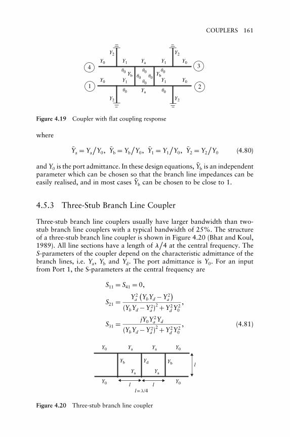
COUPLERS 161
4
1
3
2
Y2 Y2
Y2 Y2
Y0 Y0
Y0 Y0
Y1
Y1
Yb Yb
Ya
Ya
Y1
Y1
θ0 θ0
θ0θ0 θ0
θ0
θ0 θ0
Figure 4.19 Coupler with flat coupling response
where
Ya = Ya
/Y0 Yb = Yb
/Y0 Y1 = Y1
/Y0 Y2 = Y2
/Y0 �4.80�
and Y0 is the port admittance. In these design equations, Yb is an independentparameter which can be chosen so that the branch line impedances can beeasily realised, and in most cases Yb can be chosen to be close to 1.
4.5.3 Three-Stub Branch Line Coupler
Three-stub branch line couplers usually have larger bandwidth than two-stub branch line couplers with a typical bandwidth of 25%. The structureof a three-stub branch line coupler is shown in Figure 4.20 (Bhat and Koul,1989). All line sections have a length of �
/4 at the central frequency. The
S-parameters of the coupler depend on the characteristic admittance of thebranch lines, i.e. Ya, Yb and Yd. The port admittance is Y0. For an inputfrom Port 1, the S-parameters at the central frequency are
S11 = S41 = 0
S21 = Y 2a
(YbYd −Y 2
a
)�YbYd −Y 2
a �2 +Y 2d Y 2
0
S31 = jY0Y2a Yd
�YbYd −Y 2a �2 +Y 2
d Y 20
(4.81)
Y0
Yb
Ya
Yd Yb
Ya
Ya Ya Y0
Y0 Y0
l = λ /4l
l
l
Figure 4.20 Three-stub branch line coupler

162 DESIGN OF MICROWAVE CIRCUITS
Table 4.2 Three-stub branch line coupler design
S21 S31 Ya Yb Yd
0 dB 90� coupler 0 −j Y0 Y0 Y0
3 dB 90� coupler 1√2
−j√2
√2Y0
(√2−1
)Y0
√2Y0
with
(Y 2
b +Y 20
)Yd = 2YbY
2a � �4.82�
Using the three-stub configuration, it is possible to design a 0 dB coupler.The required values of Ya, Yb and Yd for the design are listed in Table 4.2.Similarly the parameters for a 3 dB coupler can also be obtained. They arelisted in Table 4.2.
4.5.4 Coupled Line Couplers
Couplers can also be realised using coupled lines (Pozar, 1990; Bhat andKoul, 1989). The diagram of a single section backwave coupled line coupleris shown in Figure 4.21. The length of the coupled line section is l = �
/4
at the central frequency. With the definition of the voltage coupling factor,Cv = �Z0e −Z0o�/�Z0e +Z0o�, the voltages at Ports 3 and 2 normalised to thevoltage at the input port, Port 1, are respectively
∣∣∣∣V3
V1
∣∣∣∣2
= C2� sin2
1−C2� cos2
�
∣∣∣∣V2
V1
∣∣∣∣2
= 1−C2�
1−C2� cos2
�4.83�
where = �l and = �/
2 at the central frequency. Port 4 is an isolated port.At the central frequency, �V3/V1�2 = C2
� and �V2/V1�2 = 1−C2� . For design
purpose, the even and odd mode characteristic impedances of the coupledline are determined by the requirement of coupling strength Cv or CvdB =20 log10 Cv from
Z0e = Z0
√1+Cv
1−Cv
� Z0o = Z0
√1−Cv
1+Cv
� �4.84�
3
1
4
2
Figure 4.21 Coupled line coupler

HYBRID RINGS 163
The physical length of the line is determined by one of the two ways, i.e.
��e +�o�
2l = �
2or
2�e�o
�e +�ol = �
2� �4.85�
The bandwidth of the coupled line coupler measured with ±0�2dBderivation is typically 40%.
4.6 HYBRID RINGS
Hybrid rings are also the devices for the control of power flow. They aredesigned with transmission lines arranged in a ring format. Some designsare described below (Bhat and Koul, 1989).
4.6.1 Hybrid Ring Coupler
A hybrid ring that can be used as a coupler is shown in Figure 4.22 (Pon,1961). The three line sections on the top half of the ring have a length of�/
4 at the central frequency, and the line section on the bottom half hasa length of 3�
/4. The port admittance of the four-port device is Y0. The
S-parameters of the hybrid ring coupler at the central frequency are
S� =
⎡⎢⎢⎣
0 −jYb 0 jYa
−jYb 0 −jYa 00 −jYa 0 −jYb
jYa 0 −jYb 0
⎤⎥⎥⎦ �4.86�
with
Y 2a + Y 2
b = 1 �4.87�
41
32
λ /4
λ /4
3λ /4
λ /4
Y0
Ya
Ya
Ya Ya
Y0
Y0Y0
Figure 4.22 Hybrid ring coupler

164 DESIGN OF MICROWAVE CIRCUITS
where
Ya = Ya
/Y0 and Yb = Yb
/Y0 �4.88�
are the normalised characteristic admittances of the line sections shown inFigure 4.22. When an input is made at Port 1, outputs at Ports 2 and 4 areout of phase by 180�, and Port 3 is isolated. When an input is made at Port3, outputs at Ports 2 and 4 are in phase and Port 1 is isolated. The powersplits depend on the values of Ya and Yb.
4.6.2 Rat-Race Hybrid
The rat-race hybrid is a special case of the hybrid ring described inSection 4.6.1, when Ya = Yb = Y0
/√2.
The S-parameters of the rat-race hybrid at the central frequency are
S� =
⎡⎢⎢⎢⎣
0 −j√2
0 j√2−j√
20 −j√
20
0 −j√2
0 −j√2
j√2
0 −j√2
0
⎤⎥⎥⎥⎦ � �4.89�
The rat-race hybrid is therefore a 3 dB coupler with good isolationbetween Ports 1 and 3 and between Ports 2 and 4 and useful bandwidth oftypically 20%.
4.6.3 Wideband Rat-Race Hybrid
The bandwidth of the rat-race hybrid in Section 4.6.2 is limited by theproperties of the 3�
/4 section of the ring. A 3 dB rat-race hybrid with
wideband response was proposed by March (1968) and is shown inFigure 4.23. The hybrid consists of three transmission line sections of length�/
4 and a coupled line section of the same length. Two opposite ends ofthe coupled line sections are short-circuited so that it effectively becomes atwo-port device connected in the ring format. The characteristic impedancesof the line sections for the 3dB hybrid are determined by
Zr = 1�46Z0� ZI = Zr =√Z0oZ0e� Z0e =(1+√
2)
Zr� Z0o =(√
2−1)
Zr
�4.90�
where Z0 is the port impedance. The ±0�3 derivation bandwidth of thewideband hybrid coupler can be over an octave. The isolation is greaterthan 20 dB.

HYBRID RINGS 165
λ /4
λ /4
λ /4
λ /4
Z0
Z0
Z0
Zr Zr
ZI Zr
Z0
Figure 4.23 Wideband rat-race hybrid
4.6.4 Modified Hybrid Ring
Theconversionalhybridringcoupler inSection4.6.1maybedifficult torealisewhen the power split is large. A modified design to overcome this problemproposed by Agrawal and Mikucki (1986) is shown in Figure 4.24. Thering has six �
/4 transmission line sections with two values of characteristic
impedance, Z1 and Z2. For different power split ratios, the values of Z1 andZ2 are tabulated in Table 4.3 for a port impedance of Z0 = 50�.
4.6.5 Modified Hybrid Ring with Improved Bandwidth
A modified hybrid ring with improved bandwidth is shown in Figure 4.25.The structure was proposed by Kim and Naito (1982). All line sectionshave a length of �
/4 at the central frequency. The optimum values of the
characteristic admittance of the line sections for the improved bandwidthof a 3 dB hybrid ring coupler are
Y1 = 0�88034Y0 Y2 = 1�34850Y0 Y3 = 3�57850Y0
Y4 = 7�7350Y0 Y1c = 1�05570Y0 Y2c = 1�72860Y0 (4.91)
λ /4 λ /4
λ /4
λ /4
λ /4
λ /4
Z1
Z1 Z1Z2
Z2 Z231
42
Figure 4.24 Modified hybrid ring

166 DESIGN OF MICROWAVE CIRCUITS
Table 4.3 The modified characteristics impedances of the lines fortwo hybrid-ring couplers (Agrawal and Mikucki, 1986)
Modified hybrid ring
Power-split ratio (dB) Z1��� Z2���
0.0 70�7 70�71.0 72�3 66�92.0 74�5 63�83.0 77�3 61�14.0 80�8 59�05.0 84�9 57�16.0 89�8 55�67.0 95�6 54�48.0 102�3 53�59.0 109�9 52�7
10.0 118�6 52�111.0 128�4 51�612.0 139�4 51�213.0 151�9 50�914.0 165�9 50�715.0 181�6 50�5
31
42
Y1
Y3Y0 Y2c
Y0
Y1c
Y0Y1c
Y2c Y0
Y4
Y3
Y2 Y2
Figure 4.25 Modified hybrid ring with improved bandwidth
where Y0 is the port admittance. The bandwidth of the optimised 3 dBcoupler is 50.67%.
4.7 PHASE SHIFTERS
Phase shifters can be realised using ferrite, discrete or lumped inductors orcapacitors, transmission lines and active components (Pozar, 1990). Twotypes of passive phase shifters are described below.
4.7.1 Transmission Line Phase Shifter
A transmission line phase shifter is made of a section of transmission linewith characteristic impedance Z0 which is the same as the port impedance,

PHASE SHIFTERS 167
as shown in Figure 4.26. The S-parameters of the transmission line sectionof length L and phase constant � are given by
S� =[
0 e−j
e−j 0
]�4.92�
where = �L. Hence the transmission between two ports has a phase delayof , and both ports are fully matched.
4.7.2 LC Phase Shifters
LC phase shifters can be made of discrete inductor and capacitorcomponents connected in ‘T’, ‘�’, to ‘L’ networks. For an ‘L’ network phaseshifter as shown in Figure 4.27 with normalised impedance and admittancequantities x and b, the S-parameters are
S� =
[−xb+ j�x−b� 22 −xb+ j�x−b�
]�2−xb�+ j�x+b�
� �4.93�
The phase shifter has an insertion loss of
�S21� = 2√�2−xb�2 + �x+b�2
�4.94�
and a phase shift
= arctan(
x+b
2−xb
)�4.95�
It is noted that such a phase shifter is not fully matched at both ports. Thereflections at the ports are
�S11� = �S22� =√
�xb�2 + �x−b�2
�2−xb�2 + �x+b�2� �4.96�
Z0
L
Figure 4.26 Transmission line phase shifter

168 DESIGN OF MICROWAVE CIRCUITS
jx (L or C)
jb (L or C )
Figure 4.27 ‘L’ network discrete element phase shifter
In the special case that x = 0, the insertion loss and phase shift are,respectively,
�S21� = 1√1+b2/4
�4.97�
and
= arctan�b/2�� �4.98�
4.8 FILTERS
4.8.1 Maximally Flat Response
The insertion loss of a low-pass filter with maximally flat response has thefollowing form (Pozar, 1990; Matthaei, Young and Jones, 1965):
PLR = 1+�2N1 �4.99�
where N is the order of the filter and the 3 dB cut-off frequency is at �c = 1.The insertion loss is shown in Figure 4.28 for different values of N .
4.8.2 Chebyshev Response
The insertion loss of a low-pass filter with Chebyshev response or equalripples in the pass band has the following form (Pozar, 1990; Matthaei,Young and Jones, 1965):
PLR = 1+k2T 2N ��� �4.100�
where 1+k2 is the pass band ripple level, TN ��� is a Chebyshev polynomialof order N and
TN �x� = cos(N cos−1 x
)for �x� < 1 and TN �x� = cosh
(N cosh−1
x)
for �x� > 1�4.101�

FILTERS 169
PL
R(ω
1, N
)
50
40
30
20
10
00 0.5 1 1.5 2
N = 8N = 9
N = 7
N = 6
N = 5
N = 4
N = 3
N = 2
N = 1
ω1
Figure 4.28 Maximally flat response PLR��1�N�
with
TN �0� ={
0 for N odd1 for N even and TN �1� = 1� �4.102�
The cut-off frequency of the low-pass filter is at �c = 1. The insertionloss is shown in Figure 4.29 for different values of N .
4.8.3 Maximally Flat Low-Pass Filters with �c = 1
The circuits of maximally flat low-pass filters with �c = 1 for a generatorimpedance R0 = 1� and load resistance RN+1 = 1� are shown inFigure 4.30(a) and (b), respectively, for a prototype beginning with a shuntcapacitor and a prototype beginning with a series inductor. A total ofN capacitors or inductors are used for a filter of order N . The elementvalues, gk, for both prototypes are given by (Matthaei, Young and Jones,1965)
g0 = 1
gk = 2sin(
�2k−1��
2N
)for k = 12 · · · N
gN+1 = 1 (4.103)

170 DESIGN OF MICROWAVE CIRCUITS
0.50 1
(a)
1.5 2
N = 9N = 7
N = 5
N = 3
N = 1
ω1
80
60
40
20
0
PL
R(ω
1, 3
dB
, N)
N = 9
N = 7
N = 5
N = 3
N = 1
0.50 1
(b)
1.5 2ω1
80
60
40
20
0
PL
R(ω
1, 0
.5 d
B, N
)
(c)
PL
R(ω
1, 0
.1 d
B, N
)
N = 7
N = 5
N = 3
N = 1
0.50 1 1.5 2ω1
80
60
40
20
0
Figure 4.29 Chebyshev response PLR��1,Ripple Level,N�: (a) 3 dB ripple level, (b)0.5 dB ripple level and (c) 0.1 dB ripple level

FILTERS 171
R0 = g0 = 1 L2 = g2
L1 = g1
G0 = g0 = 1
L3 = g3
(a)
(b)
C1 = g1
C2 = g2
C3 = g3 gN + 1
gN + 1
L4 = g4
Figure 4.30 Filter prototypes: (a) prototype beginning with a capacitor and (b)prototype beginning with an inductor
Table 4.4 gk values for maximally flat low-pass filters with g0 = 1,gN+1 = 1 and �c = 1 (Matthaei, Young and Jones, 1965)
N g1 g2 g3 g4 g5
1 2�00002 1�4142 1�41423 1�0000 2�0000 1�00004 0�7654 1�8478 1�8478 0�76545 0�6180 1�6180 2�0000 1�6180 0�6180
and gk for k = 12 � � � N is an inductance value for a series inductor anda capacitance value for a shunt capacitor. The values of gk for N = 1 − 5are tabulated in Table 4.4.
4.8.4 Chebyshev Low-Pass Filters with �c = 1
The circuits of Chebyshev low-pass filters with �c = 1 for a generatorimpedance R0 = 1� and load resistance RN+1 = 1� are shown similar tothose shown in Figure 4.30(a) and (b). However, for Chebyshev low-passfilters with RN+1 = 1�, the order N must be an odd number, i.e., N =135 � � � . Once N is determined, both prototypes consist of N inductorsor capacitors. The element values, gk, for both prototypes are given by(Matthaei, Young and Jones, 1965)
g0 = 1
g1 = 2a1
/�AR
gk = 4ak−1ak
bk−1gk−1for k = 23 � � � N
gN+1 = 1 �for odd N only� (4.104)

172 DESIGN OF MICROWAVE CIRCUITS
where
ak = sin[
�2k−1��
2N
]for k = 12 � � � N
bk = �AR2 + sin2
(k�
N
)for k = 12 � � � N
�AR = sinh(
�AR
2N
)
�AR = ln(
cothLAR
17�37
)
LAR = 10 log10�1+k2� = ripple level in dB� (4.105)
The element value gk can be an inductance value for a series inductor or acapacitive value for a shunt capacitor. The values of gk for N = 13579and ripple level of 0.5, 0.1 and 3 dB are tabulated in Table 4.5.
4.8.5 Filter Transformations
The low-pass filter prototypes described in Sections 4.8.3 and 4.8.4 are forthe case that R0 = 1� RN+1 = 1� and the cut-off frequency is �c = 1.These low-pass prototypes can be readily transformed to a low-pass filter(LPF) with a cut-off frequency �LP, a high-pass filter (HPF) with a high-pass
Table 4.5 gk values for Chebyshev low-pass filters with g0 = 1, gN+1 = 1 and �c = 1(Matthaei, Young and Jones, 1965)
N g1 g2 g3 g4 g5 g6 g7 g8 g9
Ripple = 0.5 dB1 0�69863 1�5963 1�0967 1�59635 1�7058 1�2296 2�5408 1�2296 1�70587 1�7372 1�2583 2�6381 1�3444 2�6381 1�2583 1�73729 1�7504 1�2690 2�6678 1�3673 2�7239 1�3673 2�6678 1�2690 1�7504
Ripple = 0.1 dB1 0�30523 1�0315 1�1474 1�03155 1�1468 1�3712 1�9750 1�3712 1�14687 1�1811 1�4228 2�0966 1�5733 2�0966 1�4228 1�18119 1�1956 1�4425 2�1345 1�6167 2�2053 1�6167 2�1345 1�4425 1�1956
Ripple = 3 dB1 1�99533 3�3487 0�7117 3�34875 3�4817 0�7618 4�5381 0�7618 3�48177 3�5182 0�7723 4�6386 0�8039 4�6386 0�7723 3�51829 3�5340 0�7760 4�6692 0�8118 4�7272 0�8118 4�6692 0�7760 3�5340

FILTERS 173
Table 4.6 Frequency projections
LPF HPF BPF BSF
�1 = �
�LP�1 = −�HP
��1 = 1
�
(�
�0− �0
�
)�1 = �
(�
�0− �0
�
)−1
� = 2�f � = 2�f � = f2 − f1
f0� = f2 − f1
f0
�LP = 2�fLP �HP = 2�fHP �0 = 2�f0 �0 = 2�f0
� = 2�f � = 2�f
band-edge frequency �HP, a bandpass filter (BPF) at a central frequency f0
with bandwidth �f2 − f1� a bandstop filter (BSF) at a central frequency f0
with bandwidth �f2 − f1� and in all cases above with R0 = RN+1 = Z0.The frequency projections for these transformations are tabulated in
Table 4.6 (Pozar, 1990; Bahl, 1997). These projections are used to determinethe order of the filter needed to meet the attenuation requirement atfrequencies outside the band of interest.
For the transformation to a low-pass filter, the series element gk isreplaced by an inductor Lk and the shunt element gk by a capacitor Ck.
For the transformation to a high-pass filter, the series element gk is replacedby a series capacitor Ck and the shunt element gk by an inductor Lk.
For the transformation to a bandpass filter, the series element gk isreplaced by an inductor Lk and a capacitor Ck connected in series. Theshunt element gk is replaced by an inductor Lk and a capacitor Ck connectedin parallel.
For the transformation to a bandstop filter, the series element gk isreplaced by an inductor Lk and a capacitor Ck connected in parallel. Theshunt element gk is replaced by an inductor Lk and a capacitor Ck connectedin series.
The values of Lk and Ck for these transformations are given in Table 4.7(Pozar, 1990; Bahl, 1997).
4.8.6 Step Impedance Low-Pass Filters
A step impedance low-pass filter is made of short transmission line sectionsof high or low characteristic impedance, e.g., Zhigh = 150� and Zlow = 10�,as shown in Figure 4.31 (Pozar, 1990). The low-pass filter is designed inthe usual way using the procedures described in Sections 4.8.1–4.8.5. Butthe series inductor Lk is replaced by a high-impedance line section with alength lk given by

174 DESIGN OF MICROWAVE CIRCUITS
Table 4.7 Filter transformation (Pozar, 1990)
Element LPF HPF BPF BSF
Series gk Series L
Lk = gk
Z0
�LP
Series CCk = 1
gk�HPZ0
Series-tunedseries elementsLk = gk
Z0�0�
Ck = �gkZ0�0
Shunt-tunedseries elementsLk = gk
�Z0�0
Ck = 1gk��0Z0
Shunt gk Shunt C
Ck = gk
1�LPZ0
Shunt L
Lk = Z0
gk�HP
Shunt-tunedshunt elements
Lk = �Z0
gk�0
Ck = gk
�0�Z0
Series-tunedshunt elements
Lk = Z0
gk��0
Ck = gk
�
�0Z0
Z0 Z0
l1 l2 l3 lN
Figure 4.31 Step impedance low-pass filter
�lk = LkZ0
Zhigh �4.106�
where � is the phase constant at the central frequency. The shunt capacitorCk is replaced by a low-impedance line with a length lk given by
�lk = CkZlow
Z0� �4.107�
In all cases, �l < �/
4.
4.8.7 Bandpass and Bandstop Filters Using �/4Resonators
At microwave frequencies, bandpass and bandstop filters can be realisedusing �/4 resonators as shown in Figure 4.32 (Pozar, 1990). The length ofthe line section or the spacing l between the stubs is also �/4, so that = �l =�/2. If the stubs are short-circuited at their ends, the filter has a bandpassresponse. If they are open-circuited, the filter has a bandstop response. Therequired characteristic impedances for the bandpass response are
Z0n = �Z0�
4gn
for n = 1 toN �4.108�

FILTERS 175
Z0N Z01Z02Z0N – 1
Z0Z0Z0 Z0 Z0
θ
θ
θ θ θ
All open stubs – BSF
All short stubs – BPF
Z0
Figure 4.32 Bandpass and bandstop filters using �/4 resonators
where Z0 is the source impedance and also the characteristic impedanceof the line sections connecting the stubs, and � is the relative bandwidthgiven in Table 4.6.
Similarly those for bandstop response are given by
Z0n = 4Z0
�gn
for n = 1 to N� �4.109�
For equal-ripple designs, N must be an odd number.
4.8.8 Bandpass Filters Using �/4 Connecting Lines andShort-Circuited Stubs
Figure 4.33 shows an alternative design of bandpass filters using �/4connecting lines and short-circuited stubs (Pozar, 1990; Bhat and Koul,1989; Matthaei, Young and Jones, 1965). All line sections are �/4 long atthe central frequency. The procedures for designing this type of filter are asfollows:
(1) Map the frequency to �1 domain
�1 = 2(
�−�0
�0
)� = f2 − f1
f0 f0 = f1 + f2
2 � = 2�f �0 = 2�f0
�4.110�
where f0 is the central frequency and �f2 − f1� defines the bandwidth.
Y12 Y23
Y1 YnYn–1
Yn–1, n
Y3Y2
λ /4λ /4
Figure 4.33 Bandpass filters using �/4 connecting lines and short-circuited stubs

176 DESIGN OF MICROWAVE CIRCUITS
(2) Use the attenuation requirements and low-pass filter response curvesin Figure 4.28 or 4.29 to determine the order N required, where Nis also the number of stubs in the filter.
(3) Obtain g1g2 � � � gN values for maximally flat or Chebyshev (N =odd) response.
(4) Calculate length, i.e. �/
4, at f0.(5) Compute the characteristic admittances of connecting lines and
stubs:
1 = �
2
(1− �
2
)= �
2f1
f0
Ca = 2dg1 where d = 0�5−1 but typically d = 1 is chosen,
J12
Y0=(
Ca
g2
)1/2
�Jkk+1
Y0= g0Ca√
gkgk+1 k = 2 to N −2
JN−1N
Y0=(
Ca
gN−1
)1/2
Nkk+1 =[(
Jkk+1
YA
)2
+(
Ca tan1
2
)2]1/2
k= 1 to N −1
Y1 = Y0 �1−d�g1 tan1 +Y0
(N12 − J12
Y0
)
Yk�k=2 to �N−1� = Y0
(Nk−1k +Nkk+1 − Jk−1k
Y0− Jkk+1
Y0
)
YN = Y0 �gN −dg1� tan1 +Y0
(NN−1N − JN−1N
Y0
)
Ykk+1 = Jkk+1 �for k = 1 to N −1� (4.111)
where Y0 is the source admittance and load conductance.
4.8.9 Coupled Line Bandpass Filters
Bandpass filters can also be realised using coupled lines (Pozar, 1990; Bhatand Koul, 1989; Matthaei, Young and Jones, 1965; Cohn, 1958). A diagramof the coupled line bandpass filter is shown in Figure 4.34. At the centralfrequency, the coupled line sections are �
/4 in length, where
� = 2�air(√�re +√
�ro
)

FILTERS 177
θ0
Z0
1
2
N
N + 1
l l l lZ0
Z0e Z0ol = λ /4
Figure 4.34 Coupled line bandpass filters in microstrip configuration
with �air = c/f taking the propagation of both even and odd modesinto account. The design procedures of the coupled line filter are asfollows:
(1) Map the frequency to �1 domain:
�1 = 1�
(�−�0
�0
) � = f2 − f1
f0 f0 = f1 + f2
2 � = 2�f �0 = 2�f0� �4.112�
(2) Use the attenuation requirements and low-pass filter response curvesin Figure 4.28 or 4.29 to determine the order N required. The numberof coupled line sections will be (N +1).
(3) Obtain g1g2 � � � gN values for maximally flat or Chebyshev (N =odd) response.
(4) Calculate couple line length, i.e. �/
4, at f0.(5) Compute Z0e and Z0o of the coupled lines:
Z0ek = Z0
[1+ JkZ0 + �JkZ0�
2]
Z0ok = Z0
[1− JkZ0 + �JkZ0�
2]
for k = 12 � � � N +1 (4.113)
where
J1Z0 =√
��
2g1
J2Z0 = ��
2√
g1g2
· · · � � �

178 DESIGN OF MICROWAVE CIRCUITS
JkZ0 = ��
2√
gk−1gk
Z0JN+1 =√
��
2gN
(4.114)
and Z0 is the source and load impedance.
4.8.10 End-Coupled Resonator Filters
End-coupled resonator filters, as shown in Figure 4.35, also have bandpassresponse (Pozar, 1990; Bhat and Koul, 1989). The design procedures forthe type of filter are as follows:
(1) Map the frequency to �1 domain:
�1 = 1�
(�−�0
�0
) � = f2 − f1
f0 f0 = f1 + f2
2 � = 2�f �0 = 2�f0�
�4.115�
(2) Use the attenuation requirements and low-pass filter response curvesin Figure 4.28 or 4.29 to determine the order N required. The filterwill have N resonator sections and (N +1) gaps.
(3) Obtain g1g2 � � � gN values for maximally flat or Chebyshev (N =odd) response.
(4) Calculate gap capacitance Ci:
Ci = Bi
�0 �4.116�
where
Bi = �Z0Ji�Z−10
1− �Z0Ji�2 i = 1 � � � �N +1�
Z0J1 =√
�
2g1
B1
Z0 Z0 Z0 Z0 Z0 Z0
θ1 θ2 θ3 θn
B2 B3 Bn Bn+1
Figure 4.35 End-coupled resonator filters in microstrip configuration

AMPLIFIER DESIGN 179
Z0Jk = �
2√
gk−1gk
for k = 23 � � � N
Z0JN+1 =√
�
2gN
� (4.117)
(5) Calculate resonator length li:
i = �li = � − 12
[tan−1 �2Z0Bi�+ tan−1 �2Z0Bi+1�
]� �4.118�
Again Z0 is the source and load impedance.
4.9 AMPLIFIER DESIGN
4.9.1 Maximum Gain Amplifier Design
For an amplifier with matching circuits at the input and output ends of thetransistor as shown in Figure 4.36, the transducer gain of the network ofthree blocks is (Pozar, 1990)
GT = GsG0GL =(
1−��s�2�1−�in�s�2
)(�S21�2
)( 1−��L�2�1−S22�L�2
) �4.119�
where �s, �L, �in and �out are the reflection coefficients shown in Figure 4.36.The reflection coefficients �in and �out are related to the S-parameters of thetransistor �s and �L by
�in = S11 + S12S21�L
1−S22�Land �out = S22 + S12S21�s
1−S22�s� �4.120�
The unconditionally stable conditions of the amplifier are
K = 1−�S11�2 −�S22�2 +���22 �S12S21�
> 1 and ��� = �S11S22 −S12S21� < 1�
�4.121�
Input matching circuit
Transistor[S]
Output matching
circuit
Γout ΓLΓs Γin
Z0Z0Vs
Figure 4.36 Amplifier design

180 DESIGN OF MICROWAVE CIRCUITS
The design of an amplifier with maximum gain (Pozar, 1990) requiresthat
�in = �∗s and �out = �∗
L �4.122�
so that
�s =B1 ±
(B2
1 −4 �C1�2)1/2
2C1 �L =
B2 ±(B2
2 −4 �C2�2)1/2
2C2 �4.123�
where
B1 = 1+�S11�2 −�S22�2 −��2
B2 = 1+�S22�2 −�S11�2 −��2C1 = S11 −S∗
22
� = S11S22 −S12S21� (4.124)
The maximum transducer gain is then
GT = GT max = 1(1−��s�2
) �S21�2(1−��L�2
)�1−S22�L�2
� �4.125�
For the purpose of impedance matching in the amplifier, the admittancetransformation from normalised load admittance yL = 1+ jbL to normalisedinput admittance yin = gin + jbin using a transmission line section ofcharacteristic impedance Z0 and a stub of the same characteristicimpedance, i.e. Z0, as shown in Figure 4.37 requires that
bL =√
�1−gin�2 +bin
2
gin= tan��Lstub� �4.126�
L
LOpen Stub
Yin
Z0Z 0
ZL=Z0
Figure 4.37 Amplifier impedance matching using an open-circuit stub and atransmission line section

AMPLIFIER DESIGN 181
and
tan��L� = �bin −bL��1−gin +binbL�− �1−gin��bin +ginbL�
�1−gin +binbL�2 + �bin +ginbL�2 �4.127�
where L and Lstub are the lengths of the transmission line and open-circuitedstub, respectively, and � is the phase constant. These two equations can beused to determine the length of the open-circuited stub connected in parallelto the load or source impedance of the amplifier circuit and the length ofthe transmission line section required for impedance matching at both inputand output ends of the transistor.
The impedance matching of the amplifier can also be realised usingdiscrete L and C components (Radmanesh, 2001; Rudwig and Bretchko,2000). For the requirement of the normalised impedance zin = rin + jxin withrin < 1, the impedance transformation circuit as shown in Figure 4.38(a)can be used. The required circuit elements are
Xp/Z0 = ±√
rin
1− rinand Xs/Z0 = �xin ∓√rin�1− rin��� �4.128�
Otherwise for the requirement of the normalised admittance yin = gin +jbin with gin < 1, the admittance transformation circuit as shown inFigure 4.38(b) can be used. The required circuit elements are
Xs/Z0 = ±√
1−gin
ginand Xp/Z0 = −�bin ±√gin�1−gin��
−1� �4.129�
4.9.2 Broadband Amplifier Design
The amplifier discussed in Section 4.9.1 can achieve maximum gain, but itis classified as a narrow band amplifier. The bandwidth of the amplifier canbe much improved using the balanced amplifier configuration, as shownin Figure 4.39(a) (Radmanesh, 2001). The balanced amplifier consists oftwo maximum gain amplifiers designed as in Section 4.9.1 and two 3 dBcouplers. The first coupler splits the input signal into two parts with a
Zin
jXS jXS
jXP jXP
Yin
(a) (b)
ZL=Z0 ZL=Z0
Figure 4.38 Amplifier impedance matching circuits for (a) rin < 1 and (b) gin < 1

182 DESIGN OF MICROWAVE CIRCUITS
(a)
(b)
Amp1
Amp2
3 dBcoupler
3 dBcoupler
Inputport
1
4
2
3
1
4
2
3
To matchedlead
To matchedlead
Outputport
3 dBpowerdivider
3 dBpowerdivider
1
2
3
1
2
3 Outputport
Amp1
Amp2
Inputport
λ /4transformer
λ /4transformer
Figure 4.39 Balanced amplifier using (a) 3 dB couplers and (b) 3 dB power dividers
phase difference of 90�. The signals are amplified by Amp1 and Amp2,respectively, and combined at the output. In the case that the two amplifiers,Amp1 and Amp2, are identical, the signals combined at the output are inphase at the central design frequency. The S-parameters of the balancedamplifier in terms of power transfer at the central design frequency f0 are
�S�f0��2 =[
0 �S21amp�f0��2�S12amp�f0��2 0
] �4.130�
where the subscript amp refers to the value for a single amplifier Amp1or Amp2. The power transfer of the balanced amplifier is the same as asingle amplifier Amp1 or Amp2. But it has very good impedance matchingcharacteristics at both input and output ports.
The 3 dB couplers can be made of branch line couplers. They may alsobe replaced by Wilkinson power dividers together with two quarter-wavetransformers (Rudwig and Bretchko, 2000). The first power divider splitsthe input power into two equal amounts of the same phase. One of thequarter-wave transformers is used to shift the phase of a signal in onebranch by 90� at the central frequency before amplification, and the othertransformer in the other branch by the same phase angle after amplification.Both signals are then combined in phase by the second power divider.
4.9.3 High-Frequency Small Signal FET Circuit Model
At microwave frequencies, the characteristics of active devices are usuallydescribed by their S-parameters. However, equivalent circuits have also beenused to represent active devices, particularly for small signal operations(Weber, 2001; Soares, 1988). An equivalent circuit for a FET operatingunder small signal condition is shown in Figure 4.40 as an example. The

AMPLIFIER DESIGN 183
G D
S S
Cgs
Cgd
CdsgdsVgs gmVgs
Figure 4.40 Equivalent circuit for FET
S-parameters of the equivalent circuit for a common source configurationwith respective port admittance Y0 are given by
S11 = �Y0 −Ygg��Y0 +Ydd�+YgdYdg
�Y0 +Ygg��Y0 +Ydd�−YgdYdg� S12 = −2YgdY0
�Y0 +Ygg��Y0 +Ydd�−YgdYdg�
S21 = −2YdgY0
�Y0 +Ygg��Y0 +Ydd�−YgdYdg� S22 = �Y0 +Ygg��Y0 −Ydd�+YgdYdg
�Y0 +Ygg��Y0 +Ydd�−YgdYdg
(4.131)
where (Soares, 1988)
Ygg = j��Cgs +Cgd�� Ygd = −j�Cgd� Ydg = gm − j�Cgd� Ydd = gds + j��Cds +Cgd��
(4.132)
Some typical circuit element values are Cgs = 0�5 pF Cgd =0�05pF Cds = 0�1pF ggd = 5mS and gm = 50mS�
4.9.4 Negative Feedback Amplifier Design
An amplifier with negative feedback can have flat gain response over avery wide frequency band. Such an amplifier also has good input andoutput impedance matching characteristics. It is used when broadbandamplifiers such as the balanced amplifier described in Section 4.9.2 failsto meet bandwidth requirement. An amplifier with negative feedback usingFET is shown in Figure 4.41(a). It consists of a series element R1 anda shunt element R2. The equivalent circuit of the amplifier is shownin Figure 4.41(b). The S-parameters of the circuit with respective portimpedance Z0 are given by (Radmanesh, 2001)
S� =
⎡⎢⎢⎣
1− gmZ02
R2�1+gmR1�
2Z0
R22Z0
R2− 2gmZ0
�1+gmR1�1− gmZ0
2
R2�1+gmR1�
⎤⎥⎥⎦[1+ 2Z0
R2+ gmZ0
2
R2�1+gmR1�
]−1
�
�4.133�

184 DESIGN OF MICROWAVE CIRCUITS
GD
FET
R1 R1
S
R2 R2G D
SVgs
gmVgs
(a) (b)
Figure 4.41 (a) Negative feedback amplifier and (b) its equivalent circuit
If both input and output ports are required to be matched so that S11 =S22 = 0, the minimum requirement for gm is that
gm ≥ R2
Z02� �4.134�
In this case,
S21 = Z0 −R2
Z0and S12 = Z0
R2 +Z0 �4.135�
which depend on R2 and Z0 only.If the characteristics of FET is described by S-parameters, the connection
of FET with a series resistor R1 as shown in Figure 4.42(a) can be taken asa series-to-series connection of two networks as shown in Figure 4.42(b).The resultant S-parameters can be obtained as
S�FETR1�� = −h� − S�FET��− S�R1��� �4.136�
where
S�R1�� =
⎡⎢⎢⎣
−12R1
Z02R1
Z0−1
⎤⎥⎥⎦[1+ 2R1
Z0
]−1
�4.137�
GD
FETFET
R1 R1
S
(a) (b)
Figure 4.42 (a) FET with a resistor connected to its source terminal and (b) itsnetwork presentation

REFERENCES 185
and the function h� S1� S2�� has been given in section 1.6.3. The FET-R1
combined network is again in a parallel-to-parallel connection with the R2
network. The S-parameters of the R2 network are
S�R2�� =
[R2 2Z0
2Z0 R2
]R2 +2Z0
� �4.138�
The S-parameters of the amplifier are therefore
S� = h� S�FETR1�� S�R1���� �4.139�
REFERENCES
Agrawal, A.K. and Mikucki, G.F. (1986) ‘A printed circuit hybrid ring directionalcoupler for arbitrary power division’, IEEE Transactions on Microwave Theory andTechniques, MTT-34, 1401–7.
Bahl, I.J. (1997) ‘Chapter 3: Filters, hybrids, and couplers, power combiners andmatching networks’, in Handbook of Microwave and Optical Components – Vol. 1:Microwave Passive and Antenna Components (ed. K. Chang), John Wiley & Sons,Ltd, New York, pp 118–90.
Bhat, B. and Koul, S.K. (1989) Stripline-Like Transmission Lines for MicrowaveIntegrated Circuits, John Wiley & Sons, Ltd, New York.
Cohn, S.B. (1958) ‘Parallel-coupled transmission line resonator filter’, IEEE Transactionson Microwave Theory and Techniques, MTT-6, 223–31.
Cohn, S.B. (1968) ‘A class of broadband three-port TEM-mode hybrids’, IEEETransactions on Microwave Theory and Techniques, MTT-16, 110–6.
Collin, R.E. (1966) Foundations for Microwave Engineering, McGraw-Hill, New York.Ginzton, E.L. (1957) Microwave Measurements, McGraw-Hill, New York.Kim, D.I. and Naito, Y. (1982) ‘Broadband design of improved hybrid-ring 3dB
directional coupler’ ‘IEEE Transactions on Microwave Theory and Techniques, MTT-30, 2040–6.
March, S. (1968) ‘A wideband strip line hybrid ring’, IEEE Transactions on MicrowaveTheory and Techniques, MTT-16, 361.
Matthaei, G.L., Young, L. and Jones, E.M.T. (1965) Microwave Filters, ImpedanceMatching Networks and Coupling Structures, McGraw-Hill, New York.
Parad, L.I. and Moynihan, R.L. (1965) ‘Split-tee power divider’, IEEE Transactions onMicrowave Theory and Techniques, MTT-13, 91–5.
Pon, C.Y. (1961) ‘Hybrid ring directional coupler for arbitrary power division’, IRETransactions on Microwave Theory and Techniques, MTT-9, 529–35.
Pozar, D.M. (1990) Microwave Engineering, Addison-Wesley, New York.Radmanesh, M.M. (2001) Radio Frequency and Microwave Electronics Illustrated,
Prentice Hall, Englewood Cliffs, NJ.Riblet, G.P. (1978) ‘A directional coupler with very flat coupling’, IEEE Transactions
on Microwave Theory and Techniques, MTT-26, 70–4.Rudwig, R. and Bretchko, P. (2000) RF Circuit Design, Theory and Applications,
Prentice Hall, Englewood Cliffs, NJ.

186 DESIGN OF MICROWAVE CIRCUITS
Soares, R. (ed.) (1988) GaAs MESFET Circuit Design, Artech House, London.Weber, R.J. (2001) Introduction to Microwave Circuits: Radio Frequency and Design
Applications, IEEE Press.Wu, Z. and Davis, L.E. (1994) ‘Automation-orientated techniques for quality factor
measurement of high-Tc superconducting resonators’, IEE Proceeding Part A, 141(6), 527–30.

5Simulation of MicrowaveDevices and Circuits
ABSTRACT
In this chapter, examples of the devices described in Chapter 3 and thecircuits designed using the principles or procedures described in Chapter 4are presented. The simulation of the designed circuits using the CircuitSimulator described in Chapter 2 is also illustrated. Each circuit example issaved in the circuit holder of the same name as the circuit for easy reference,and all the examples are contained in the CD enclosed.
KEYWORDS
Microwave circuits, Transmission lines, Impedance matching, Impedancetransformers, Resonators, Power dividers, Couplers, Filters, Amplifierdesign, Wireless transmission systems
As detailed in Chapter 3, the Software VNA has 35 built-in devices.The properties of each device can be simulated with various inputs andinvestigated using the display and marker functions of the Software VNA.The start and stop frequencies can be chosen to have a wide or closeview of the S-parameter responses. With the design principles describedin Chapter 4, a great number of microwave circuits can be designed fordifferent applications. In this chapter, examples of the devices describedin Chapter 3 and the circuits designed using the principles or proceduresdescribed in Chapter 4 are presented. The simulation of the designed circuitsusing the Circuit Simulator described in Chapter 2 is also illustrated. Eachcircuit example is saved in the circuit holder of the same name as the circuitfor easy reference. All the examples in this chapter are contained in the CDand should be copied to the computer manually during the installation.
Software VNA and Microwave Network Design and Characterisation Zhipeng Wu© 2007 John Wiley & Sons, Ltd

188 SIMULATION OF MICROWAVE DEVICES AND CIRCUITS
5.1 TRANSMISSION LINES
5.1.1 Terminated Transmission Line
Figure 5.1(a) shows the circuit of a terminated transmission line withcharacteristic impedance Z0 = 100�, length l = 0�15m, phase velocity vp =c where c is the speed of light in air and load impedance ZL = 50�. The
Z0 = 100 Ω
l = 0.15 m
vp = c ZL = 50 Ω
(a)
(b)
(c)
Figure 5.1 Terminated transmission line: (a) circuit diagram, (b) assembled circuitand (c) simulation results

TRANSMISSION LINES 189
circuit can be simulated by defining a transmission line section and a loadresistance using the Circuit Simulator. The assembled circuit, Tline_ttl.nwk,is shown in Figure 5.1(b). Port 1 of the Software VNA is connected tothe input port of the transmission line device, and the resistive load isconnected to the output port of the transmission line. With the settings ofstart frequency to 0.5 GHz and stop frequency to 2.5 GHz, the simulatedS11 response is shown in Figure 5.1(c). At 1 GHz, �S11� has a very smallvalue. At this frequency, the transmission line is one half-wavelength long,and the input impedance is the same as the load impedance, i.e. 50�. Thisrepeats at 2, 3 GHz and so on when the length of the transmission line isan integer number of half-wavelengths.
5.1.2 Two-Port Transmission Line
Figure 5.2(a) shows a lossless transmission line section in two-portconfiguration. The transmission line has a characteristic impedance Z0 =100�, length l = 0�15m and phase velocity vp = c. The frequencyresponses of this transmission line section can be simulated using theGeneral Transmission Line device described in Section 3.6. The device,Tline_2ptl.dev, is shown in Figure 5.2(b). With the settings of startfrequency to 0.5 GHz and stop frequency to 2.5 GHz, the simulated S21
response is shown in Figure 5.2(c). At 1 GHz, the transmission line is onehalf-wavelength long so that �S21� has the largest value, i.e. �S21� = 1 (or0 dB). This repeats at 2, 3 GHz and so on. At 0.5, 1.5 GHz and so on, thelength of the transmission line is an odd number of quarter-wavelengthsso that �S21� has the minimum value. The S11 response is the same as theexample in Section 5.1.1.
5.1.3 Short-Circuited Transmission Line Stub
Figure 5.3(a) shows a short-circuited transmission line stub. Thetransmission line stub is lossless and has a characteristic impedance Z0 =50�, length l = 0�075m and phase velocity vp = c. The frequency responsesof this transmission line section can be simulated using the Two-PortParallel Transmission Line Stub device described in Section 3.8. The device,Tline_scs.dev, is shown in Figure 5.3(b). The simulated S21 response isshown in Figure 5.3(c), with the start frequency of 0.5 GHz and stopfrequency of 2.5 GHz. At 2 GHz, the transmission line stub is one half-wavelength long so that the input end of the stub is effectively short-circuited. The short-circuited stub has therefore a bandstop response around2 GHz and multiples of 2 GHz.

190 SIMULATION OF MICROWAVE DEVICES AND CIRCUITS
(a)
(b)
(c)
Z0 = 100 Ω
l = 0.15 m
vp = c
Figure 5.2 Two-port transmission line: (a) circuit diagram, (b) assembled circuitand (c) simulation results
5.1.4 Open-Circuited Transmission Line Stub
Figure 5.4(a) shows an open-circuited transmission line stub. Thetransmission line stub is lossless and has a characteristic impedance Z0 =50�, length l = 0�075m and phase velocity vp = c. The frequency responsesof this transmission line section can also be simulated using the Two-Port Parallel Transmission Line Stub device described in Section 3.8. The

TRANSMISSION LINES 191
(a)
(b)
(c)
0.075
m
S/c
Z0 = 50 Ωvp = c
Figure 5.3 Short-circuited transmission line stub: (a) circuit diagram, (b) assembledcircuit and (c) simulation results
device, Tline_ocs.dev, is shown in Figure 5.4(b). The simulated S21 responseis shown in Figure 5.4(c), with the start frequency of 0.5 GHz and stopfrequency of 2.5 GHz. At 1 GHz, the transmission line stub is one quarter-wavelength long so that the input end of the stub is effectively short-circuited. The open-circuited stub has therefore a bandstop response around1 GHz and odd multiples of 1 GHz.

192 SIMULATION OF MICROWAVE DEVICES AND CIRCUITS
(a)
(b)
(c)
0.075 m
O/c
Z0 = 50 Ωvp = c
Figure 5.4 Open-circuited transmission line stub: (a) circuit diagram, (b) assembledcircuit and (c) simulation results
5.1.5 Periodic Transmission Line Structures
Figure 5.5(a) shows a periodic structure made of microstrip line sectionsand open-circuited stubs. The purpose of this example is to illustrate thefiltering response of the structure. The microstrip lines and stubs are madeof RT/Duroid 5880 with the following parameters: �r = 2�2, w = 2�575mm,

TRANSMISSION LINES 193
(a)
(b)
(c)
2 cm2 cm
O/cO/c
2 cm2 cm
Figure 5.5 Periodic transmission line structure: (a) circuit diagram, (b) assembledcircuit and (c) simulation results
h = 0�79mm, L = 2cm. The width of the line, w, is chosen using theMicrostrip Line device described in Section 3.15 so that Z0 = 50�.
The periodic structure can be simulated by defining the transmissionline sections and stubs, which are connected by T-junctions. The circuitassembled using the Circuit Simulator, Tline_ptls.nwk, is shown inFigure 5.5(b). Port 1 of the Software VNA is connected to the input portof the first transmission line section and Port 2 to the last transmissionline section. The start frequency is set to 0.5 GHz and stop frequency to

194 SIMULATION OF MICROWAVE DEVICES AND CIRCUITS
10 GHz. The simulated S21 response is shown in Figure 5.5(c). The periodicstructure has a low-pass response at 1.9 GHz, bandstop response at 2.7 GHzwhen the stub is a quarter-wavelength long, bandpass response at 5.4 GHz(with 3 dB bandwidth of 3.6 GHz) when the stub is one half-wavelengthlong.
The periodic structure can be modified with short-circuited stubs. Thefrequency responses of the modified periodic structure, Tline_ptls2.nwk,can be investigated further.
5.2 IMPEDANCE MATCHING
5.2.1 Matching of a Half-Wavelength Dipole AntennaUsing a Discrete Element
For a dipole antenna of length 50 mm made of a metallic wire of radiusa = 0�5mm, the dipole is one half-wavelength long at f0 = 3GHz. Theinput impedance of the dipole at 3 GHz can be obtained using the DipoleAntenna device described in Section 3.30, with the use of Smith chartdisplay and frequency span from 2 to 4 GHz. The dipole antenna is shownin Figure 5.6(a). The input impedance and admittance of the antennaat 3 GHz are Zant�f0� = 73�13 + j42�54� and Yant�f0� = Gant�f0�+jBant�f0� =0�010217− j0�005943S, respectively. The reflection coefficient at 3 GHz is�S11�f0�� = −8�6dB without matching. The dipole antenna can be matchedusing a capacitor connected in parallel with the antenna and a quarter-wavetransformer. The required capacitance value is
C = −Bant�f0�
2�f0= 3�153×10−13 F = 0�3153pF
and the characteristic impedance of the transformer is
Z0 =√
50G−1ant�f0� = 69�96��
The length of the transformer is 25 mm with vp = c, which is onequarter-wavelength at 3 GHz. The matching circuit can be assembled usingthe Circuit Simulator with a dipole antenna, a capacitor, a transmissionline section and the parameters calculated above. The input end of thetransmission line section is connected to Port 1 of the Software VNA. Thecircuit, Matching_de.nwk, is shown in Figure 5.6(b). The simulated resultsare shown in Figure 5.6(c) with the frequency span from 1 to 5 GHz. Thedipole is well matched at 3 GHz with −10dB bandwidth of 17.8% from2.75 to 3.24 GHz.

IMPEDANCE MATCHING 195
(a)
(b)
(c)
C
λ /4
Z0 Zant
Figure 5.6 Matching of a dipole antenna using a discrete element: (a) circuitdiagram, (b) assembled circuit and (c) simulation results
5.2.2 Single Stub Matching of a Half-Wavelength DipoleAntenna
The half-wavelength dipole of length 50 mm and wire radius 0.5 mmshown in Figure 5.6(a) can also be matched using the single stub matchingtechnique described in Section 4.1.2. The input impedance of the dipoleat f0 = 3GHz is Zant�f0� = 73�13 + j42�54�. Using the equations inSection 4.1.2, the required lengths of the transmission line section andshort-circuited stub with Z0 = 50� can be calculated to be l1 = 0�02142mand l2 = 0�014254m, respectively. The matching circuit can be assembledusing the Circuit Simulator with a dipole antenna, a 50� transmission line

196 SIMULATION OF MICROWAVE DEVICES AND CIRCUITS
section, a 50� stub and the specified lengths above. The input end of thetransmission line stub is connected to Port 1 of the Software VNA. Thecircuit, Matching_ss.nwk, is shown in Figure 5.7(a). The simulated resultsare shown in Figure 5.7(b) with the frequency span from 1 to 5 GHz. Thedipole is well matched at 3 GHz with −10dB bandwidth of 13.9% from2.8 to 3.19 GHz.
(a)
(b)
(c)
Zant
S/c stub
l2
l1
v p = c
vp = c
Z0 = 50 Ω
Z = 50 Ω
Figure 5.7 Single stub matching of a dipole antenna: (a) circuit diagram, (b)assembled circuit and (c) simulation results

IMPEDANCE TRANSFORMERS 197
5.3 IMPEDANCE TRANSFORMERS
5.3.1 Quarter-Wave Impedance Transformer
Figure 5.8(a) shows the design of a quarter-wave impedance transformerwhich transforms the load resistance RL = 10 − 50� input impedance
ZL = RL = 10 Ω
λ /4 = 25 mm
Z0 = 22.36 Ω
vp = c
(a)
(b)
(c)
Figure 5.8 Quarter-wave impedance transformer: (a) circuit diagram, (b)assembled circuit and (c) simulation results

198 SIMULATION OF MICROWAVE DEVICES AND CIRCUITS
at 3 GHz. The length of transmission line with vp = c is 25 mm. Thecharacteristic impedance of the line can be calculated using the equation inSection 4.2.1, i.e.
Z0 = √50×10 = 22�36��
The theoretical bandwidth of the transformer at VSWR = 1�5 is 29%.Using the Circuit Simulator, the assembled quarter-wave transformer
circuit, Ztrans_qw.nwk, is as shown in Figure 5.8(b). It consists of atransmission line section and a resistive load with the parameters specifiedabove. The input end of the transformer is connected to Port 1 of theSoftware VNA. The simulated results are shown in Figure 5.8(c) withthe frequency span from 1 to 5 GHz. Using the VSWR display, it can bedetermined that the quarter-wave transformer has a bandwidth of 29.3%at VSWR = 1�5.
5.3.2 Chebyshev Multisection Impedance Transformer
Figure 5.9(a) shows the design of a four-section Chebyshev impedancetransformer using the equations in Section 4.2.2 with the maximumreflection in the matched band �m = 0�2, the central frequency f0 = 3GHz,load resistance RL = 100� and source impedance Zs = Z0 = 50�. Alltransmission line sections with vp = c are 25 mm in length, which is /4long at 3 GHz. The required characteristic impedances of the line sectionsare calculated to be (Pozar, 1990)
Z01 = 63�13� Z02 = 67�48� Z03 = 72�31� and Z04 = 77�30��
Theoretically, for N = 4 �m = 0�2, RL = 100� and Z0 = 50�,
sec�m = cosh[
14
cosh−1(
10�2
∣∣∣∣100−50100+50
∣∣∣∣)]
= cosh[
14
cosh−1(
53
)]
so that �m = 15�54� = 0�27126rad and the bandwidth is
�f
f0�at VSWR=1�5or�m=0�2 = 2− 4�m
�= 1�655 = 165�5%�
Using the Circuit Simulator, the assembled quarter-wave transformercircuit, Ztrans_Cheby.nwk, is as shown in Figure 5.9(b). The simulatedresults are shown in Figure 5.9(c) with the frequency span from 0 to 6 GHz.Chebyshev ripples can be observed in the display. Using the VSWR format,it can be determined that the four-section impedance transformer has abandwidth of 163% at VSWR = 1�5 from 0.6 to 5.5 GHz. The maximum

IMPEDANCE TRANSFORMERS 199
(a)
(b)
(c)
Z01 Z02 Z03 Z04ZL = RL = 100 Ω
λ /4 λ /4 λ /4 λ /4
Figure 5.9 Chebyshev multisection impedance transformer: (a) circuit diagram, (b)assembled circuit and (c) simulation results
reflection in the matched band is �m = 0�21 with the assigned transmissionline parameters, which can be seen using the linear display, LinM.
5.3.3 Corporate Feeds
Figure 5.10(a) shows two corporate feeds that are commonly used inthe impedance matching of antenna arrays. In the first design, two 50�lines are connected in parallel. The resultant impedance is transformed to50� using a 35�36� quarter-wave transformer. In the second design, two70�7 � quarter-wave transformers are used. Each transformer transforms

200 SIMULATION OF MICROWAVE DEVICES AND CIRCUITS
λ /4
50 Ωfeed
Z0 = 35.36 ΩZ0 = 50 Ω
Z0 = 50 Ω
λ /4
λ /450 Ω line
50 Ω line
50 Ω line
Z0 = 70.7 Ω line50 Ωfeed
Configuration 1 Configuration 2
(a)
(b)
(c)
Figure 5.10 Corporate feeds: (a) circuit diagrams, (b) assembled circuit ofconfiguration 1 and (c) simulation results of configuration 1
the 50� load impedance to an impedance of 100 � at the centralfrequency. The transformed impedances are connected in parallel togive a resultant impedance of 50�. In both designs, the length of each

IMPEDANCE TRANSFORMERS 201
transformer is 25 mm for a central frequency of 3 GHz when a transmissionline with vp = c is used.
The assembled circuit for the first design, Corpfeed_35.nwk, is shownin Figure 5.10(b). The 50 � load impedance is represented by a MatchedLoad. The simulated results with a frequency span from 0 to 6 GHz areshown in Figure 5.10(c). The impedance is very well matched at 3 GHz.Using the VSWR display, it can be seen that the VSWR values of bothcorporate feeds are always less than 2. The assembled circuit for the seconddesign, Corpfeed_70.nwk, can also be simulated in the same way.
5.3.4 Corporate Feeds Realised Using Microstrip Lines
The corporate feeds discussed in Section 5.3.4 can be realised usingmicrostrip lines. Figure 5.11(a) shows the microstrip version of the design inFigure 5.10(a), realised using RT/Duroid 5880 with �r = 2�2 and substratethickness h = 0�79mm. By setting the start frequency to 3 GHz and usingthe Microstrip Line device described in Section 3.15, the width and thelength of the 50� microstrip line can be determined or chosen to be
w1 = 2�48mm L =
4= 0�018161m for �re = 1�895�
Similarly the width and the length of the 35.36 � microstrip line can bedetermined to be
w2 = 4�14mm L =
4= 0�017839m for �re = 1�964�
The assembled circuit, Corpfeed_35m.nwk, is shown in Figure 5.11(b).The 50� load impedance is again represented by a Matched Load. Thesimulated results with a frequency span from 0 to 6 GHz are shown inFigure 5.11(c). The impedance is also very well matched at 3 GHz.
5.3.5 Kuroda’s Identities
Kuroda’s identities are often used in microwave filter design usingtransmission lines (Pozar, 1990). Figure 5.12(a) and (b) shows one ofKuroda identities. It shows that an open-circuited stub of characteristicimpedance Z2 and length /8 connected with a transmission line section ofcharacteristic impedance Z1 and length /8 is equivalent to a transmissionline section of characteristic impedance Z2/n2 and length /8 connectedwith a short-circuited stub of characteristic impedance Z1/n2 and length/8 where
n2 = 1+Z2
/Z1�

202 SIMULATION OF MICROWAVE DEVICES AND CIRCUITS
(a)
(c)
λ/4
50 Ωfeed
Z0 = 35.36 Ω
Z0 = 50 Ω
Z0 = 50 Ω
Configuration 1
(b)
Figure 5.11 Corporate feed using microstrip lines: (a) circuit diagram, (b)assembled circuit and (c) simulation results

IMPEDANCE TRANSFORMERS 203
(c)
(d)
Z1Z2n2
Z1
n2
Z0 = Z1
Z 0 = Z 2
λ /8λ /8
λ /8O/c
S/c
Port 1Port 1
Port 2Port 2
(a) (b)
1/Z2
Z0 = 25 ΩZ0 = 25 Ω
Figure 5.12 Kuroda’s identities: (a) and (b) identity circuits, (c) and (d) assembledcircuits and (e) and (f) simulation results

204 SIMULATION OF MICROWAVE DEVICES AND CIRCUITS
(e)
(f)
Figure 5.12 ( Continued)
When a transmission line with vp = c is used, all line sections have alength of 12.5 mm. Taking
Z1 = Z2 = 50�
for the circuit in Figure 5.12(a), the characteristic impedance of theline section and stub of the circuit in Figure 5.12(b) can be calculatedto be
Z2
n2= 25�
with n2 = 2. The assembled circuits for Figure 5.12(a) and (b), i.e.Kuroda_1a.nwk and Kuroda_1b.nwk, are shown in Figure 5.12(c)and (d), respectively. The simulation results with the frequency span

RESONATORS 205
from 1 to 10 GHz of these two circuits are shown in Figure 5.12(e)and (f), respectively. The identity of both circuits can be examinedin terms of all S-parameters and also in terms of amplitude andphase.
5.4 RESONATORS
5.4.1 One-Port RLC Series Resonant Circuit
Figure 5.13(a) shows a one-port directly connected RLC series resonantcircuit with
R = 10� L = 30nH C = 0�03pF�
The resonance frequency of the resonant circuit is
f0 = 1
2�√
LC= 5�3GHz
and the unloaded and loaded Q-factors are
Q0 = 0L
R=√
L/
C
R= 100
and
QL = 0L
R+Z0= 1000
10+50= 16�7
respectively. The resonant circuit can be simulated using the One-PortImpedance Load device described in Section 3.3 as Reson_1psr.dev, withthe frequency span from 5.1 to 5.5 GHz. The results of the �S11� response areshown in Figure 5.13(b). Use Marker 1 to locate the resonance frequencyand the Q0 and QL measurement functions to measure their values. TheQ-factors can be more accurately measured with a smaller frequency spanor an increased number of frequency points.
5.4.2 Two-Port RLC Series Resonant Circuit
Figure 5.14(a) shows the same RLC series resonant circuit as that inSection 5.4.1 but in two-port connections. The resonance frequency andunloaded Q-factor remain the same. But the loaded Q-factor is changed to
QL = 0L
R+2Z0= 1000
110= 9�09�

206 SIMULATION OF MICROWAVE DEVICES AND CIRCUITS
CR L
(a)
(b)
(c)
Figure 5.13 One-port RLC series resonant circuit: (a) circuit diagram, (b)assembled circuit and (c) simulation results
The resonant circuit can be simulated using the Two-Port SingleImpedance device described in Section 3.4 as Reson_2psr.dev, with thefrequency span from 5.1 to 5.5 GHz. The results of the �S21� response areshown in Figure 5.14(b). Use Marker 1 to locate the resonance frequencyand the Q0 and QL measurement functions to measure their values. TheQ-factors can be measured using either S21 or S11 display. The resonance
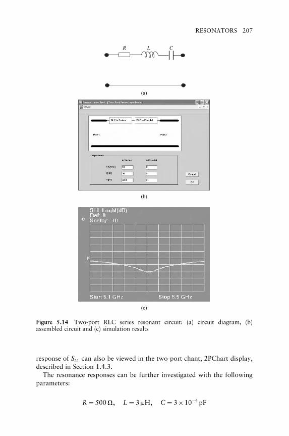
RESONATORS 207
(a)
(b)
(c)
R L C
Figure 5.14 Two-port RLC series resonant circuit: (a) circuit diagram, (b)assembled circuit and (c) simulation results
response of S21 can also be viewed in the two-port chant, 2PChart display,described in Section 1.4.3.
The resonance responses can be further investigated with the followingparameters:
R = 500� L = 3�H C = 3×10⁻⁴ pF
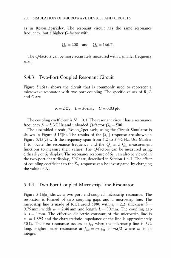
208 SIMULATION OF MICROWAVE DEVICES AND CIRCUITS
as in Reson_2psr2dev. The resonant circuit has the same resonancefrequency, but a higher Q-factor with
Q0 = 200 and QL = 166�7�
The Q-factors can be more accurately measured with a smaller frequencyspan.
5.4.3 Two-Port Coupled Resonant Circuit
Figure 5.15(a) shows the circuit that is commonly used to represent amicrowave resonator with two-port coupling. The specific values of R, Land C are
R = 2� L = 30nH C = 0�03pF�
The coupling coefficient is N = 0�1. The resonant circuit has a resonancefrequency f0 = 5�3GHz and unloaded Q-factor Q0 = 500.
The assembled circuit, Reson_2pcr.nwk, using the Circuit Simulator isshown in Figure 5.15(b). The results of the �S21� response are shown inFigure 5.15(c) with the frequency span from 5.2 to 5.4 GHz. Use Marker1 to locate the resonance frequency and the Q0 and QL measurementfunctions to measure their values. The Q-factors can be measured usingeither S21 or S11display. The resonance response of S21 can also be viewed inthe two-port chart display, 2PChart, described in Section 1.4.3. The effectof coupling coefficient to the S21 response can be investigated by changingthe value of N .
5.4.4 Two-Port Coupled Microstrip Line Resonator
Figure 5.16(a) shows a two-port end-coupled microstrip resonator. Theresonator is formed of two coupling gaps and a microstrip line. Themicrostrip line is made of RT/Duroid 5880 with �r = 2�2, thickness h =0�79mm, width w = 2�48mm and length L = 30mm. The coupling gapis s = 1mm. The effective dielectric constant of the microstrip line is�re = 1�895 and the characteristic impedance of the line is approximately50�. The first resonance occurs at f01 when the microstrip line is /2long. Higher order resonance at f0m = m f01 is m/2 where m is aninteger.
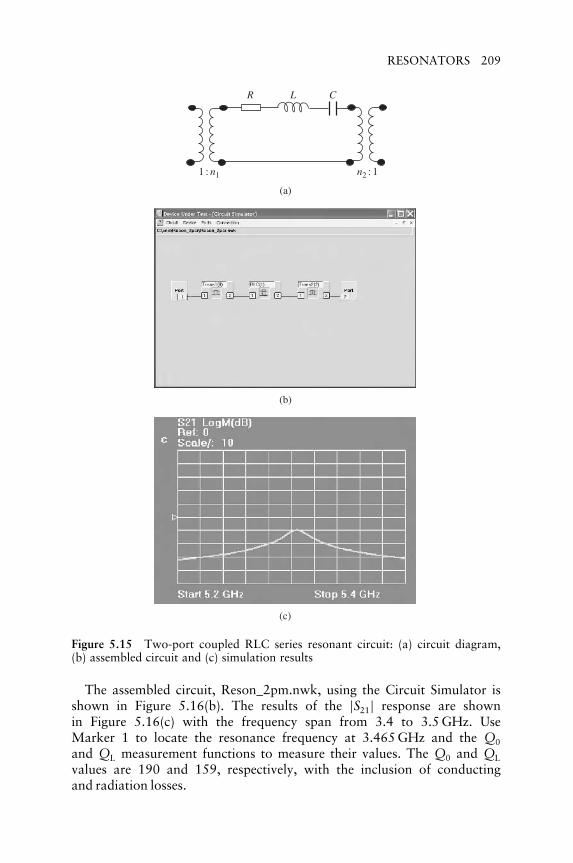
RESONATORS 209
(b)
(a)
(c)
R L
1 : n1 n2 : 1
C
Figure 5.15 Two-port coupled RLC series resonant circuit: (a) circuit diagram,(b) assembled circuit and (c) simulation results
The assembled circuit, Reson_2pm.nwk, using the Circuit Simulator isshown in Figure 5.16(b). The results of the �S21� response are shownin Figure 5.16(c) with the frequency span from 3.4 to 3.5 GHz. UseMarker 1 to locate the resonance frequency at 3.465 GHz and the Q0
and QL measurement functions to measure their values. The Q0 and QL
values are 190 and 159, respectively, with the inclusion of conductingand radiation losses.

210 SIMULATION OF MICROWAVE DEVICES AND CIRCUITS
(a)
(b)
(c)
Line
30 mm1 mm 1 mm
Line LineGapGap
Port 1 Port 2
λ /2
Figure 5.16 Two-port coupled microstrip line resonator: (a) resonator layout,(b) assembled circuit and (c) simulation results
5.4.5 Two-Port Coupled Microstrip Coupled LineResonator
Figure 5.17(a) shows a two-port coupled microstrip coupled line resonator.The resonator is formed of two coupling gaps and a microstrip coupled

RESONATORS 211
λ/2(a)
(b)
(c)
30 mm
Line
Line Coupled line
Gap
Gap
O/c
O/c
s = 1 mm
Figure 5.17 Two-port coupled microstrip coupled line resonator: (a) resonatorlayout, (b) assembled circuit and (c) simulation results
line. The coupled line is made of RT/Duroid 5880 with �r = 2�2, thicknessh = 0�79mm, width w = 2�48mm and length L = 30mm. The coupling gapis s = 1mm. The first even and odd mode resonances occur when the lengthof the coupled line is e/2 or o/2.
The assembled circuit, Reson_2pcm.nwk, using the Circuit Simulator isshown in Figure 5.17(b). The results of the �S21� response are shown inFigure 5.17(c) with the frequency span from 3.4 to 3.8 GHz. Use Marker 1

212 SIMULATION OF MICROWAVE DEVICES AND CIRCUITS
to locate the resonance frequencies of the even mode at 3.48 GHz and oddmode at 3.64 GHz. Use the Q0 and QL measurement functions to measuretheir values. The Q0 value of the even mode is lower than that of the oddmode due to a higher loss of the even mode.
5.4.6 Two-Port Symmetrically Coupled Ring Resonator
Figure 5.18(a) shows a two-port symmetrically coupled ring resonator. Theresonator is formed of two coupling gaps and a microstrip ring. The ring
(a)
(b)
(c)
Port 1 Port 2
1 mm 1 mm
Circumference = 30 mm
Figure 5.18 Two-port symmetrically coupled ring resonator: (a) resonator layout,(b) assembled circuit and (c) simulation results

POWER DIVIDERS 213
is made of RT/Duroid 5880 with �r = 2�2, thickness h = 0�79mm, widthw = 2�48mm and circumference 60 mm. The coupling gap is s = 1mm.The effective dielectric constant of the microstrip line is �re = 1�895 andthe characteristic impedance of the line is approximately 50�. The firstresonance frequency is estimated to be at 3.47 GHz when the circumferenceof the ring is one wavelength.
The assembled circuit, Reson_rings.nwk, using the Circuit Simulator isshown in Figure 5.18(b). The ring is represented by two transmissionlines connected in parallel, and two T-junctions are used to connect thetransmission lines and the coupling gaps. The results of the �S21� responseare shown in Figure 5.18(c) with the frequency span from 3.4 to 3.6 GHz.Use Marker 1 to locate the resonance frequency at 3.542 GHz, which isdifferent from the theoretical value due to the effect of the coupling gaps.Using the Q-factor measurement functions, the Q0 and QL factors aremeasured to be 196 and 177, respectively, with the inclusion of conductingand radiation losses.
5.4.7 Two-Port Asymmetrically Coupled Ring Resonator
Figure 5.19(a) shows a two-port asymmetrically coupled ring resonator.The resonator is made of RT/Duroid 5880 with �r = 2�2, thickness h =0�79mm, width w = 2�48mm and circumference 60 mm. However, the ringis coupled asymmetrically with an arc length of 31.5 mm at the top and28.5 mm at the bottom. The resonator is coupled by two transformers withN = 0�01.
The assembled circuit, Reson_ringas.nwk, using the Circuit Simulatoris shown in Figure 5.19(b). The ring is represented by two transmissionlines of different lengths connected in parallel, and two T-junctions areused to connect the transmission lines and the transformers. The resultsof the �S21� response are shown in Figure 5.19(c) with the frequency spanfrom 3.3 to 3.9 GHz. Due to the asymmetrical coupling, there exist twoclosely spaced resonances in the frequency range. Use Marker 1 to locatethe resonance frequencies at 3.456 and 3.816 GHz. The Q0 and QL factorsof the resonances can also be measured with a smaller frequency span usingthe Q-factor measurement functions.
5.5 POWER DIVIDERS
5.5.1 3 dB Wilkinson Power Divider
Figure 5.20(a) shows the design of a 3 dB Wilkinson power divider describedin Section 4.4.1 with a central frequency f0 = 3GHz. For the port impedance

214 SIMULATION OF MICROWAVE DEVICES AND CIRCUITS
(a)
(b)
(c)
Port 2
Port 1
31.5 mm
28.5 mm
Figure 5.19 Two-port asymmetrically coupled ring resonator: (a) resonator layout,(b) assembled circuit and (c) simulation results
of Z0 = 50�, the characteristic impedance of the quarter-wave transmissionline sections is
√2Z0 = 70�7 �, and the length of the line is 25 mm assuming
vp = c. The resistance of the isolation resistor connecting the two arms isR = 100�.

POWER DIVIDERS 215
(b)
(c)
(a)
Port
λ/4
λ/4 Z0
Z0
Z0 2Z0 = R1
2
3
Port
Port
2Z0
2Z0
Figure 5.20 3 dB Wilkinson power divider: (a) circuit diagram, (b) assembledcircuit and (c) simulation results
The Wilkinson power divider can be assembled using the CircuitSimulator as shown in Figure 5.20(b). The circuit, Divider_3dB.nwk,consists of two transmission lines, a series resistor in two-port connection,three T-junctions and a Matched Load. The Matched Load is used toterminate Port 3 of the power divider. Port 2 of the power divider serves asthe measurement port, which is connected to Port 2 of the Software VNA.

216 SIMULATION OF MICROWAVE DEVICES AND CIRCUITS
The S21 response is shown in Figure 5.20(c) with the frequency span from 1to 5 GHz. The S21 value at 3 GHz is −3�01dB, which can be identified usingMarker 1. The 0.2 dB coupling deviation bandwidth is 82.7% from 1.76to 4.24 GHz. Using the Phase display, it can be seen that there is a phasedelay of 90� at 3 GHz at the output port, which agrees with the theoreticalvalue in Section 4.4.1.
When the VSWR of the reflection response, S11, is displayed, it canbe measured that the bandwidth at VSWR = 1�22 is 37% from 2.44 to3.56 GHz.
It is possible to disconnect Port 2 of the Software VNA and the MatchedLoad and exchange their connections so that Port 3 of the power divider isconnected to Port 2 of the Software VNA. Similar observations of the S21
and S11 responses can be made.If Port 1 of the Software VNA and the Matched Load are both
disconnected and their connections are exchanged, the isolation responsebetween Ports 2 and 3 of the power divider can be observed from the S21
display. At 3 GHz, the isolation between the two ports is 82.4 dB.
5.5.2 Microstrip 3 dB Wilkinson Power Divider
The 3 dB Wilkinson power divider in Section 5.5.2 can be realised usingmicrostrip lines. Figure 5.21(a) shows the microstrip version of the 3 dBWilkinson power divider, made of RT/Duroid 5880 with �r = 2�2 andthickness h = 0�79mm. Using the Microstrip Line device described inSection 3.15 and setting the start frequency to 3 GHz, the width of therequired 70�7 � line section at 3 GHz can be found to be w = 1�392mm,and the effective relative dielectric constant at 3 GHz is �re = 1�823. Hencethe length of the line section is
L =
4= 0�025√
�re= 0�018516m�
With these parameters, the circuit of the microstrip 3 dB Wilkinson powerdivider can be assembled and the radiation losses of the microstrip linescan be included in the modelling. The circuit, Divider_3dBm.nwk, is shownin Figure 5.21(b) with Port 2 of the power divider connected to Port 2of the Software VNA. The S21 response of the power divider is shown inFigure 5.21(c) with the frequency span from 1 to 5 GHz. The S21 value at3 GHz is −3�04dB. The 0.2 dB deviation bandwidth is 82.7% from 1.68to 4.16 GHz. Using the Phase display, it can be seen that there is a phasedelay of 90�01� at 3 GHz at the output port, which agrees well with thetheoretical value. The VSWR and isolation responses can be observed inthe same way as those in Section 5.5.1.

POWER DIVIDERS 217
(a)
(b)
(c)
2 Z0
2 Z0
Z0
Z0
Z0
R = 2Z0
λ /4
λ /4
Figure 5.21 Microstrip 3 dB Wilkinson power divider: (a) circuit diagram, (b)assembled circuit and (c) simulation results
5.5.3 Cohn’s Cascaded 3 dB Power Divider
Figure 5.22(a) shows the design of Cohn’s cascaded power divider with3 dB division at f0 = 3GHz using the equations in Section 4.4.4. For N = 2

218 SIMULATION OF MICROWAVE DEVICES AND CIRCUITS
(a)
(b)
(c)
1
2
3
Port
Port
Port
λ /4λ /4
λ /4 λ /4
Z0
Z0
Z0R1R2
Z1Z2
Z2 Z1
Figure 5.22 Cohn’s cascaded 3 dB power divider: (a) circuit diagram, (b) assembledcircuit and (c) simulation results
and the frequency bandwidth ratio of f2
/f1 = 2, the required Z1, Z2, R1
and R2 values are (Cohn, 1968)
Z1 = 1�2197 ×50 = 60�99�� Z2 = 1�6398×50 = 81�99��
R1 = 4�8204×50 = 241�� R2 = 1�9602×50 = 98��

COUPLERS 219
The length of the quarter-wavelength transmission line sections withvp = c is
/4 = 0�025m. With these parameters, the circuit of the
power divider can be assembled, as shown in Figure 5.22(b). The circuit,Divider_3Cohn.nwk, consists of four transmission line sections, twoisolation resistors, five T-junctions and a Matched Load. With Port 2 of theSoftware VNA connected to Port 2 of the divider, the simulated results ofthe S21 response are shown in Figure 5.22(c) with the frequency span from 1to 5 GHz. The value at 3 GHz is 3.02 dB. The 0.2 dB deviation bandwidth is112.7% from 1.16 to 4.84 GHz, which is wider than the Wilkinson powerdivider. Using the Phase display, it can be seen that the phase delay at theoutput port at 3 GHz is 180�.
When the VSWR of the reflection response, S11, is displayed, it canbe measured that the bandwidth at VSWR = 1�22 is 84% from 1.76 to4.28 GHz.
When Ports 1 and 2 of the Software VNA are connected to Ports 2 and 3of the power divider, as in Divider_3Cohn2.nwk, the isolation response canbe observed from the S21display. The isolation at 3 GHz is 27.3 dB, whichis worse than the Wilkinson power divider.
5.6 COUPLERS
5.6.1 Two-Stub Branch Line Coupler
Figure 5.23(a) shows the design of a 3 dB 90� two-stub branch line couplerwith the central frequency of f0 = 3GHz. The characteristic impedancesof the line sections are Za = 35�4� and Zb = 50�. The length of theline sections with vp = c is 25 mm. The circuit of the branch line couplerassembled using the Circuit Simulator, Coupler_2sbl.nwk, is shown inFigure 5.23(b) with the frequency span from 1 to 5 GHz. It consists offour line sections, four T-junctions and two Matched Loads. Port 2 ofthe Software VNA is connected to Port 3 of the coupler. The results ofthe coupling response, �S21�, are shown in Figure 5.23(c). The couplingstrength at 3 GHz is −3dB and the phase delay is 180�. The 0.2 dB deviationbandwidth is 33.3% from 2.5 to 3.5 GHz. The return loss at 3 GHz is over57 dB at both ports.
If the connections of Port 2 of the Software VNA and the Matched Loadat Port 2 of the coupler are exchanged, the direct transmission responsecan be observed. The phase delay at 3 GHz is 90�. Similarly if Port 2 ofthe Software VNA is connected to Port 4 of the coupler, the isolationcharacteristics can be observed.
For a design of 10 dB 90� two-stub branch line coupler with the centralfrequency of f0 = 3GHz, the characteristic impedances of the line sections

220 SIMULATION OF MICROWAVE DEVICES AND CIRCUITS
(a)
(b)
(c)
λ /4
λ /4
Z0
Z0 Z0
Z0
Z0
Z0 / 2
Z0 / 2
Figure 5.23 Two-stub branch line coupler: (a) circuit diagram, (b) assembled circuitand (c) simulation results
are required to be Za = 47�4� and Zb = 150�. The coupling, directtransmission and isolation responses of the coupler can be simulated usingthe circuit assembled in Coupler_2sbl2.nwk.

COUPLERS 221
5.6.2 Microstrip Two-Stub Branch Line Coupler
The 3 dB 90� two-stub branch line coupler in Section 5.6.1 can be realisedusing the microstrip line made of RT/Duroid 5880 with �r = 2�2 andthickness h = 0�79mm. Using the Microstrip Line device described inSection 3.15 and setting the start frequency to 3 GHz, the width of therequired 35�4� line section at 3 GHz can be found to be wa = 4�14mm,and the effective relative dielectric constant at 3 GHz is �re = 1�964.The length of the 35.4 � line section is thus La = /4 = 0�01784m.Similarly for the 50� line section, wb = 2�48mm, �re = 1�895 and Lb =/4 = 0�01816m. With these parameters, the circuit of the microstrip3 dB 90� two-stub branch line coupler can be assembled. The radiationlosses of the microstrip lines can be included in the modelling. Thecircuit, Coupler_2sblm.nwk, is shown in Figure 5.24(a) with Port 2 ofSoftware VNA connected to Port 3 of the coupler. The S21 responseof the power divider is shown in Figure 5.24(b) with the frequencyspan from 1 to 5 GHz. The S21 value at 3 GHz is −3�09dB. The directtransmission or isolation response can also be observed when Port 2of the Software VNA is connected to Port 2 or Port 4 of the coupler,respectively.
5.6.3 Three-Stub Branch Line Coupler
Figure 5.25(a) shows the design of a 0 dB 90� three-stub branch linecoupler with the central frequency of f0 = 3GHz. The characteristicimpedances of the line sections are Za = 50�, Zb = 50� and Zd =50�. The length of the line sections with vp = c is 25 mm. Thecircuit of the branch line coupler assembled using the Circuit Simulator,Coupler_3sbl.nwk, is shown in Figure 5.25(b) with the frequency spanfrom 1 to 5 GHz. It consists of seven line sections, six T-junctionsand two Matched Loads. Port 2 of the Software VNA is connected toPort 3 of the coupler. The results of the coupling response, �S21�, areshown in Figure 5.25(c). The coupling strength at 3 GHz is 0 dB, and thephase at 3 GHz is 90� or a phase delay of 270�. The 0.2 dB deviationbandwidth is 9% from 2.5 to 3.5 GHz. The coupler is very well matchedat Port 1.
For a design of 3 dB 90� three-stub branch line coupler with thecentral frequency of f0 = 3GHz, the characteristic impedances of theline sections are required to be Za = 35�4�, Zb = 120�7 �, Zd =35�4�. The coupling, direct transmission and isolation responses of thecoupler can be simulated using the circuit assembled in Coupler_3sbl2.nwk.

222 SIMULATION OF MICROWAVE DEVICES AND CIRCUITS
(a)
(b)
(c)
21
4 3
λ /4
λ /4
Z0
Z0 Z0
Z0
Z0 Z0
Z0 / 2
Z0 / 2
Figure 5.24 Microstrip two-stub branch line coupler: (a) circuit diagram, (b)assembled circuit and (c) simulation results
5.6.4 Coupled Line Coupler
The coupled line coupler can be simulated using the Four-Port CoupledLines device described in Section 3.22. For a 10 dB coupled line coupler witha central frequency of f0 = 1�5GHz, the even and odd mode characteristic

COUPLERS 223
(a)
(b)
(c)
1
4
2
3Za Za
Za
Zb Zd Zb
Za
Figure 5.25 Three-stub branch line coupler: (a) circuit diagram, (b) assembledcircuit and (c) simulation results
impedances of the coupled line can be obtained, using the equations inSection 4.5.4, to be Z0e = 69�4� and Z0o = 36�, and the length of the lineis L = 50 mm for vp = c. Figure 5.26(a) shows the simulation input of thecoupler, Coupler_cl.dev, with Port 1 of the Software VNA connected to Port1 of the coupler and Port 2 of the Software VNA to Port 3 of the coupler.The coupling response is shown in Figure 5.26(b) with the frequency span

224 SIMULATION OF MICROWAVE DEVICES AND CIRCUITS
(b)
(a)
(c)
l = λ/4
1
3 4
2Z0e Z0o
Figure 5.26 Coupled line coupler: (a) circuit diagram, (b) assembled circuit and(c) simulation results
from 0 to 3 GHz. The coupling strength at 1.5 GHz is −9�98dB, as indicatedby Marker 1. The 0.2 dB deviation bandwidth is 29%. Port 1 of the coupleris very well matched. If Port 2 of the Software VNA is connected to Port 2

COUPLERS 225
or Port 4 of the coupler, the direct transmission and isolation responses ofthe coupler can be observed.
5.6.5 Microstrip Coupled Line Coupler
The 10 dB coupled line coupler can be realised using microstrip lines.This can be simulated using the Four-Port Coupled Microstrip Linesdevice described in Section 3.24. The device, Coupler_clm.dev, is shown inFigure 5.27(a). With the choice of RT/Duroid of �r = 2�2 and thickness h =0�79mm, the width of the microstrip lines and the spacing between the linesare determined to be w = 2�025mm and s = 0�15mm for Z0e = 69�529�and Z0o = 35�978�. At f0 = 1�5GHz, �ree = 1�94 and �reo = 1�76 so thatthe length of the line can be calculated to be L = g/4 = 0�0368m where
g = ge +go
2= 0�147174m�
The simulation results of the coupling response are shown inFigure 5.27(b) with Part 1 of the Software VNA connected to Port 1 of thecoupler. The coupling strength at 1.5 GHz is −10�25dB.
5.6.6 Rat-Race Hybrid Ring Coupler
Figure 5.28(a) shows the rat-race hybrid ring coupler (Pon, 1961), designedusing the equations in Section 4.6.2 with a central frequency of f0 =3GHz, Z0 = 50� and Za = √
2Z0 = 70�7 �. The circuit consists of threetransmission line sections of 25 mm in length and one section of 75 mmin length and four T-junctions. The coupler, Coupler_rrhr.nwk, is shownin Figure 5.28(b). The phase velocity of each transmission line section istaken to be vp = c. With Port 1 of the Software VNA connected to Port 1of the coupler and Port 2 of the Software VNA to Port 4 of the coupler,the coupling response can be observed. This coupling response is shownin Figure 5.28(c) with the frequency span from 1 to 5 GHz. The couplingstrength at 3 GHz is −3dB and the phase angle at 3 GHz is 90�. The 0.2 dBdeviation bandwidth is 22.7% from 2.66 to 3.34 GHz. If Port 2 of theSoftware VNA is connected to Port 2 of the coupler, the coupling responseto Port 2 of the coupler for an input from Port 1 can also be observed. Thecoupling strength at 3 GHz is again −3dB and the phase angle at 3 GHz is−90�. The 0.2 dB deviation bandwidth is 18.7% from 2.72 to 3.28 GHz. IfPort 2 of the Software VNA is connected to Port 3 of the coupler, it can beseen that Port 3 is very well isolated at 3 GHz.
Further examinations can be made with Port 1 of the Software VNAconnected to Port 2, 3 or 4 of the coupler and Port 2 of the Software VNAto other ports of the coupler.

226 SIMULATION OF MICROWAVE DEVICES AND CIRCUITS
(b)
(a)
(c)
1
3
2
4
Figure 5.27 Microstrip coupled line coupler: (a) circuit diagram, (b) assembledcircuit and (c) simulation results
5.6.7 March’s Wideband Rat-Race Hybrid Ring Coupler
Figure 5.29(a) shows the wideband rat-race hybrid ring coupler (March,1968), designed using the equations in Section 4.6.3 with a central frequencyof f0 = 3GHz and Z0 = 50�. The circuit consists of three transmission

COUPLERS 227
λ /4
λ/4λ/4
3λ /4
1 4
2 3
(b)
(a)
(c)
Y0
Y0 Ya
Ya
Ya
Ya
Y0
Y0
Figure 5.28 Rat-race hybrid ring coupler: (a) circuit diagram, (b) assembled circuitand (c) simulation results

228 SIMULATION OF MICROWAVE DEVICES AND CIRCUITS
(b)
(a)
(c)
λ /4
λ /4
λ /4
λ/4
Z0
Z0
Z0
Z0
Zr Zr
ZrZI
Figure 5.29 March’s wideband rat-race hybrid ring coupler: (a) circuit diagram,(b) assembled circuit and (c) simulation results

FILTERS 229
line sections, a coupled line with two short-circuited terminations at twoopposite ports and four T-junctions. The transmission line and coupledline sections have a length of 25 mm with the consideration of vp = c.The characteristic impedance of the transmission line sections is Zr = 73�.The even and odd mode characteristic impedances of the coupled line areZ0e = �1 + √
2�ZI = 176�2� and Z0o = �√
2 − 1�ZI = 30�2�, respectively.The coupler, Coupler_March.nwk, is shown in Figure 5.29(b). With Port1 of the Software VNA connected to Port 1 of the coupler and Port 2 ofthe Software VNA to Port 4 of the coupler, the coupling response can beobserved. It is shown in Figure 5.29(c) with the frequency span from 1to 5 GHz. The coupling strength at 3 GHz is −3dB and the phase angleat 3 GHz is 90�. The 0.2 dB deviation bandwidth is 56% from 2.16 to3.84 GHz. The bandwidth is increased by 2.5 times compared with the rat-race hybrid ring design in Section 5.6.6. If Port 2 of the Software VNA isconnected to Port 2 of the coupler, the coupling response to Port 2 of thecoupler for an input from Port 1 can also be observed. The coupling strengthat 3 GHz is again −3dB and the phase angle at 3 GHz is −90�. The 0.2 dBdeviation bandwidth is 62.6%. If Port 2 of the Software VNA is connectedto Port 3 of the coupler, it can be seen that the isolation at 3 GHz is −69dB.
Again further examinations can be made with Port 1 of the SoftwareVNA connected to Port 2, 3 or 4 of the coupler and Port 2 of the SoftwareVNA to other ports of the coupler.
5.7 FILTERS
5.7.1 Maximally Flat Discrete Element Low-Pass Filter
Figure 5.30(a) shows the design of a fifth order maximally flat low-passfilter with Z0 = 50� and fc = 1GHz. For N = 5, the element values given inSection 4.8.3 and Table 4.4 for c = 1 are (Pozar, 1990; Matthaei, Youngand Jones, 1965)
g0 = 1 g1 = 0�618 g2 = 1�618 g3 = 2 g4 = 1�618 g5 = 0�618 g6 = 1�
Applying the impedance and frequency scaling tabulated in Table 4.7gives
C1 = g1
/�50×2�fc� = 0�618
100� ×109= 3�09×10−12 F
L2 = g2 ×50/
�2�fc� = 1�618×502� ×109
= 12�8×10⁻⁹ H
C3 = g3
/�50×2�fc� = 2
100� ×109= 6�366×10−12 F
L4 = L2 = 12�8×10⁻⁹ H

230 SIMULATION OF MICROWAVE DEVICES AND CIRCUITS
and
C5 = C1 = 3�09×10−12 F�
Using these values, the assembled circuit, Filter_mfdelpf.nwk, is shownin Figure 5.30(b). With the selection of start frequency of 0 GHz and stopfrequency of 2 GHz, the S21 response of the low-pass filter is shown inFigure 5.30(c). The response can be viewed with different scale values andfrequency span. The cut-off frequency occurs at 1 GHz approximately.
(b)
(a)
(c)
Port 1 Port 2
L2 = g2
C1 = g1 C3 = g3 C5 = g5
L4 = g4
Figure 5.30 Maximally flat low-pass filter: (a) circuit diagram, (b) assembledcircuit and (c) simulation results

FILTERS 231
5.7.2 Equal Ripple Discrete Element Low-Pass Filter
Figure 5.31(a) shows the design of a fifth order Chebyshev equal ripplelow-pass filter with Z0 = 50� and fc = 1GHz and ripple level of 0.5 dB.For N = 5, the element values given in Section 4.8.4 and Table 4.5 for c = 1 are (Pozar, 1990; Matthaei, Young and Jones, 1965)
g0 = 1 g1 = 1�7058 g2 = 1�2296 g3 = 2�5408 g4 = 1�2296
g5 = 1�7058 g6 = 1
(b)
(a)
(c)
Port 1 Port 2
L2 = g2
C1 = g1 C3 = g3 C5 = g5
L4 = g4
Figure 5.31 Equal ripple low-pass filter: (a) circuit diagram, (b) assembled circuitand (c) simulation results

232 SIMULATION OF MICROWAVE DEVICES AND CIRCUITS
so that the element values of the low-pass filter are
C1 = g1 / �50×2�fc� = 1�7058100� ×109
= 5�43pF
L2 = g2 ×50 / �2�fc� = 1�2296×502� ×109
= 9�785nH
C3 = g3 / �50×2�fc� = 2�5408100� ×109
= 8�09pF
L4 = L2 = 9�785nH C5 = C1 = 5�43pF�
Using these values, the assembled circuit, Filter_erdelpf.nwk, is shown inFigure 5.31(b). The simulated S21 response of the low-pass filter is shownin Figure 5.31(c) with the frequency span from 0 to 2 GHz. The cut-offfrequency of the filter at −0�5dB level occurs at 1 GHz. With the scale of1 dB/Div, the ripple level of the filter can be observed.
5.7.3 Equal Ripple Discrete Element Bandpass Filter
Figure 5.32(a) shows the design of a fifth order Chebyshev equal ripplebandpass filter with Z0 = 50�, f0 = 3GHz, bandwidth of 20% or 0.6 GHzand ripple level of 0.5 dB. For N = 5, the element values given inSection 4.8.4 and Table 4.5 for c = 1 are (Pozar, 1990; Matthaei, Youngand Jones, 1965)
g0 = 1 g1 = 1�7058 g2 = 1�2296 g3 = 2�5408 g4 = 1�2296
g5 = 1�7058 g6 = 1�
Using the filter transformations in Tables 4.6 and 4.7,
L11 = L55 = 0�311nH C11 = C55 = 9�05pF
L22 = L44 = 16�31nH C22 = C44 = 0�1726pF
L33 = 0�209nH and C33 = 13�48pF
can be obtained. Using these values, the assembled circuit,Filter_erdebpf.nwk, is shown in Figure 5.32(b). The simulated S21 responseof the bandpass filter is shown in Figure 5.32(c) with the frequency spanof 2–4 GHz. Using the scale of 1 dB/Div, the equal ripple level bandpassresponse of the filter can be more clearly observed. The bandpass filter hasa sharp cut-off on both sides of the pass band. The −3dB bandwidth is20% or 0.6 GHz approximately.

FILTERS 233
(a)
(b)
(c)
Port 2Port 1
L22 L44 C44C22
L11 L33 L55C11 C33 C55
Figure 5.32 Bandpass filter: (a) circuit diagram, (b) assembled circuit and (c)simulation results
5.7.4 Step Impedance Low-Pass Filter
Figure 5.33(a) shows the design of an eighth order maximally flat low-passfilter with Z0 = 50� and fc = 1GHz. For N = 8, the element values given inSection 4.8.3 and Table 4.4 for c = 1 are (Pozar, 1990; Matthaei, Youngand Jones, 1965)
g1 = 0�3902 g2 = 1�1111 g3 = 1�6629 g4 = 1�9615
g5 = 1�9615 g6 = 1�6629 g7 = 1�1111

234 SIMULATION OF MICROWAVE DEVICES AND CIRCUITS
(b)
(c)
Port 2Port 1
L2
C1 C3 C5 C7
L4 L6 L8
l1 l2 l3 l4 l5 l6 l7 l8
(a)
Zlow = 10 Ω Zhigh = 200 Ω50 Ω 50 Ω
Figure 5.33 Microstrip step impedance low-pass filter: (a) circuit diagram, (b)assembled circuit and (c) simulation results
and
g8 = 0�3902�
By choosing Zhigh = Zh = 200� and Zlow = Zl = 10�, the phase lengths ofthe high- and low-impedance sections can be calculated using the equationsin Section 4.8.6, and they are tabulated in Table 5.1. All the phase lengthsare less than �/4 or 90�. If the high- and low-impedance sections are

FILTERS 235
realised using RT/Duroid 5880 with �r = 2�2, h = 0�79mm and t = 35�m,the physical length of each section can be calculated using
l = ��l�0
2�√
�re=
��l�c
fc
2�√
�re=
��l�× 3×10⁸
1×10⁹
2�√
�re= ��l�×0�3
2�√
�re�
With the use of the Physical Transmission Lines: Microstrip Line devicedescribed in Section 3.15, the width of each section can be found based onits characteristic impedance requirement, and the �re value can be obtainedaccordingly. The physical length of each section can be chosen to meet therequirement. These values are tabulated in Table 5.1.
Using the parameters in Table 5.1, a step impedance low-pass filter,Filter_silpf.nwk, can be assembled as shown in Figure 5.33(b). Thesimulated S21 response of the bandpass filter is shown in Figure 5.33(c)
Table 5.1 Parameters of high- and low-impedance sections
Air RT/Duroid 5880with �r = 2�2,h = 0.79 mm
No. Z0��� �l (rad) l (mm) �re l (mm) w (mm)
1 10 �l1 = C1Zl
Z0= g1Zl
Z0= 0�3902×10
50= 0�07804 = 4�47�
3�726 2�096 2�574 17�95
2 200 �l2 = LZ0
Zh
= g2Z0
Zh
= 1�1111×50200
= 0�277775 = 15�92�13�263 1�610 10�453 0�04
3 10 �l3 = g3Zl
Z0= 1�6629×10
50= 0�33258 = 19�06�
15�88 2�096 10�968 17�95
4 200 �l4 = g4Z0
Zh
= 1�9615×50200
= 0�490375 = 28�10�23�414 1�610 18�453 0�04
5 10 �l5 = g5Zl
Z0= 1�9615×10
50= 0�3923 = 22�48�
18�731 2�096 12�938 17�95
6 200 �l6 = g6Z0
Zh
= 1�6629×50200
= 0�415725 = 23�82�19�849 1�610 15�644 0�04
7 10 �l7 = g7Zl
Z0= 1�1111×10
50= 0�2222 = 12�73�
10�61 2�096 7�329 17�95
8 200 �l8 = g8Z0
Zh
= 0�3902×50200
= 0�09755 = 5�59�4�658 1�610 3�671 0�04

236 SIMULATION OF MICROWAVE DEVICES AND CIRCUITS
with the frequency span of 0–3 GHz. Using the scale of 1 dB/Div, it can beseen that the response deviates slightly from the required maximally flatlow-pass response, due to the approximations in the parameters.
5.7.5 Bandpass Filter Using Quarter-Wave Resonators
Figure 5.34(a) shows the design of a fifth order Chebyshev bandpass filterusing quarter-wavelength short-circuited stubs with Z0 = 50�, f0 = 3GHz,� = �f2 − f1�/f0 = 20% and ripple level of 0.5 dB. For N = 5, the elementvalues given in Section 4.8.4 and Table 4.5 for c = 1 are (Pozar, 1990;Matthaei, Young and Jones, 1965)
g0 = 1 g1 = 1�7058 g2 = 1�2296 g3 = 2�5408
g4 = 1�2296 g5 = 1�7058 g6 = 1�
At 3 GHz, 0 = 0�1m. If vp = c is chosen for all the transmissionline sections so that = 0, the physical length of the transmission linesections is then l = / 4 = 0�025m. Using the equation in Section 4.8.7, thecharacteristic impedance of each line section can be calculated as follows:
Z01 = Z05 = �Z0�
4g1= � ×50×0�2
4×1�7058= 4�6�
Z02 = Z04 = �Z0�
4g2= 6�39� and Z03 = 3�09��
Using these values, the assembled circuit, Filter_bpfur.nwk, is shown inFigure 5.34(b). The simulated S21 response of the bandpass filter is shownin Figure 5.34(c) with the frequency span of 2–4 GHz. Using the scale of1 dB/Div, the equal ripple level bandpass response of the filter can be moreclearly observed. The ripple level is −0�35dB. The −3dB bandwidth is 20%approximately. The bandwidth can be measured more accurately with asmaller frequency span or an increased number of points.
5.7.6 Bandpass Filter Using Quarter-Wave ConnectingLines and Short-Circuited Stubs
Figure 5.35(a) shows the design of an eighth order Chebyshev bandpassfilter using quarter-wavelength connecting lines and short-circuited stubswith Z0 = 50�, f0 = 3GHz, f1 = 1�95GHz, f2 = 4�05GHz, d = 1 and ripplelevel of 0.1 dB (Matthaei, Young and Jones, 1965). Using the procedure

FILTERS 237
(a)
(b)
λ /4
λ /4 λ /4 λ /4 λ /4
Z0 Z0
Z0N Z0N–1 Z02 Z01
Z0 Z0 Z0 Z0
All short stubs – BPF
Port 1 Port 2
N = 5
(c)
Figure 5.34 Bandpass filter using quarter-wave resonators: (a) circuit diagram, (b)assembled circuit and (c) simulation results

238 SIMULATION OF MICROWAVE DEVICES AND CIRCUITS
n = 8
Y12
Y1 Y2 Y3 Yn–1 Yn
Y23 Yn–1, n
λ/4 λ /4
(a)
(b)
(c)
Figure 5.35 Bandpass filter using quarter-wave connecting lines and short-circuitedstubs: (a) circuit diagram, (b) assembled circuit and (c) simulation results
described in Section 4.8.8, the characteristic impedances of the connectingtransmission lines and stubs are
Z12 = Z78 = 501�288
= 38�8� Z23 = Z67 = 501�364
= 36�7 �
Z34 = Z56 = 501�292
= 38�7 �

FILTERS 239
Z45 = 501�277
= 39�2� Z1 = Z8 = 501�042
= 48�
Z2 = Z7 = 502�050
= 24�4�
Z3 = Z6 = 502�049
= 24�4� and Z4 = Z5 = 502�087
= 24��
At f0 = 3GHz, 0 = 0�1m so that if vp = c is chosen for all the transmissionline sections, the physical length of the transmission line sections is l =/4 = 0�025m.
Using these values, the assembled circuit, Filter_bpfuls.nwk, is shownin Figure 5.35(b). The simulated S21 response of the bandpass filter isshown in Figure 5.35(c) with the frequency span of 1–5 GHz. Usingthe scale of 1 dB/Div, the equal ripple level bandpass response of thefilter can be more clearly observed. The −3dB bandwidth is 70%approximately.
5.7.7 Microstrip Coupled Line Filter
Figure 5.36(a) shows the design of a third order Chebyshev bandpassfilter using microstrip coupled lines with Z0 = 50�, f0 = 3GHz, � =�f2 − f1�/f0 = 20% and ripple level of 0.5 dB. The filter has four coupledline sections. Using the procedure described in Section 4.8.9 and thePhysical Coupled Lines: Two-Port Coupled Microstrip Lines device inSection 3.25, the parameters of the filter can be obtained as listedin Table 5.2 with the use of RT/Duroid 5880 with �r = 2�2, h =0�79mm and t = 35�m. The width and spacing of the microstripcoupled line are adjusted to meet the even and odd characteristicimpedance requirements. The effective relative permittivity for the evenmode and the odd mode is then obtained accordingly so that thephysical length of each section can be calculated using the equation inSection 4.8.9.
Table 5.2 Parameters for microstrip coupled line filter made of RT/Duroid 5880
n gn Z0Jn Z0e��� Z0o��� w (mm) S (mm) �ree �reo Length (m)
1 1�5963 0�4436 82 37�7 1�508 0�093 1�91 1�72 0�0185762 1�0967 0�2374 64�7 40�9 2�104 0�719 1�95 1�79 0�0182943 1�5963 0�2374 64�7 40�9 2�104 0�719 1�95 1�79 0�0182944 1 0�4436 82 37�7 1�508 0�093 1�91 1�72 0�018576
w = 2�48mm for a line with Z0 = 50�

240 SIMULATION OF MICROWAVE DEVICES AND CIRCUITS
θ0
l l l l
l = λ /4
(a)
(b)
(c)
N = 31
2
N
N + 1
Z0
Z0
Z0e Z0e
Figure 5.36 Microstrip coupled line filter: (a) circuit diagram, (b) assembled circuitand (c) simulation results
The assembled circuit, Filter_mclbpf.nwk, is shown in Figure 5.36(b).The simulated S21 response of the bandpass filter is shown in Figure 5.36(c)with the frequency span of 2–4 GHz. Using the scale of 1 dB/Div, the equalripple level bandpass response of the filter can be more clearly observed,and the ripple level is 0.5 dB approximately. The filter has a loss of 0.5 dB,partly due to the ohmic loss on the conductors.

AMPLIFIER DESIGN 241
Table 5.3 Parameters for end-coupled microstrip line filter made of RT/Duroid5880
n gn Z0Jn Bn�×10−3� Cn�pF� �n�deg� ln (m) Gap (mm)
1 1�5963 0�4436 11�046 0�586 142�7 0�028795 0�0092 1�0967 0�2374 5�032 0�267 153�3 0�030934 0�0253 1�5963 0�2374 5�032 0�267 142�7 0�028795 0�0254 1 0�4436 11�046 0�586 0�009
5.7.8 End-Coupled Microstrip Resonator Filter
Figure 5.37(a) shows the design of the third order Chebyshev bandpassfilter as that in Section 5.7.7, but realised using end-coupled microstriplines. The required filter response parameters are Z0 = 50�, f0 = 3GHz,� = �f2 − f1�/f0 = 20% and ripple level of 0.5 dB. Using the proceduresdescribed in Section 4.8.10, the Physical Transmission Lines: MicrostripLine device in Section 3.15 for the microstrip line and the Physical LineDiscontinuities: Microstrip Line Discontinuities device in Section 3.20 forthe gap, the parameters of the filter can be obtained as listed in Table 5.3with the use of RT/Duroid 5880 with �r = 2�2, h = 0�79mm and t = 35�m,in which
�n = �ln = 2�
0
√�reln and ln = �n0
2�√
�re= �n ×0�1
2�√
�re�
For the microstrip line with Z0 = 50�, it can be obtained thatw = 2�48mm and �re = 1�895 at 3 GHz. The gap distance can be obtainedby using the S11 display on the 2PChart to match the required capacitancevalue, in which the admittance value is Yn = jBn/100.
The assembled circuit, Filter_ecmrbpf.nwk, is shown in Figure 5.37(b).The simulated S21 response of the bandpass filter is shown in Figure 5.37(c)with the frequency span of 2–4 GHz. Using the scale of 1 dB/Div, the equalripple level bandpass response of the filter can be more clearly observed,and the ripple level is again 0.5 dB approximately. The filter has a loss of0.5 dB, partly due to the ohmic loss on the conductors.
5.8 AMPLIFIER DESIGN
5.8.1 Maximum Gain Amplifier
Figure 5.38(a) shows the design of an amplifier with maximum gain at2 GHz using the principle described in Section 4.9.1. The transistor usedis a Siemens CGY50 FET (Siemens, CGY50 FET datasheets), and the

242 SIMULATION OF MICROWAVE DEVICES AND CIRCUITS
(a)
(b)
(c)
B1
Z0 Z0 Z0 Z0 Z0 Z0
θ1 θ2 θ3 θN
B2 B3 BN BN+1
Figure 5.37 End-coupled microstrip filter: (a) circuit diagram, (b) assembled circuitand (c) simulation results
S-parameters of the FET at different frequencies with respect to Z0ref = 50�are listed in Table 5.4.
At 2 GHz, it can be calculated that
��� = 0�332 < 1 and K = 1�742 > 1�

AMPLIFIER DESIGN 243
0.192λ
0.039λ0.048λ
0.439λ
O/ c
O/c
Gs GL[S]
Z0 = 50 Ω
Z0 = 50 ΩZ0 = 50 Ω
Z0 = 50 ΩZL = 50 Ω
Z0 = 50 Ω
Vs
Port 1
(a)
(b)
(c)
Figure 5.38 Maximum gain amplifier: (a) circuit diagram, (b) assembled circuitand (c) simulation results

244 SIMULATION OF MICROWAVE DEVICES AND CIRCUITS
Table 5.4 S-parameters of Siemens CGY50 FET (VD = 4�5 V, VG = 0, Z0 = 50 �
S11 S21 S12 S22
f (GHz) Mag Ang Mag Ang Mag Ang Mag Ang
0.2 0�25 −31 3�30 164 0�14 5�0 0�05 −1440.4 0�27 −34 3�20 158 0�14 0�0 0�05 −1330.6 0�21 −44 3�17 150 0�13 −2�0 0�08 1050.8 0�20 −54 3�09 142 0�13 −3�0 0�01 911.0 0�19 −65 3�00 134 0�13 −4�0 0�12 811.2 0�18 −77 2�90 126 0�13 −5�0 0�14 741.4 0�18 −93 2�81 118 0�13 −5�0 0�16 681.6 0�17 −103 2�70 111 0�13 −6�0 0�17 621.8 0�17 −119 2�60 103 0�13 −5�0 0�18 562.0 0�17 −130 2�50 96 0�12 −5�0 0�19 512.2 0�18 −141 2�42 94 0�12 −4�0 0�20 462.4 0�18 −152 2�33 83 0�12 −4�0 0�21 422.6 0�19 −163 2�24 77 0�12 −3�0 0�21 392.8 0�20 −172 2�16 71 0�13 −3�0 0�21 363.0 0�21 179 2�07 65 0�13 −2�0 0�21 333.2 0�22 172 2�01 60 0�13 −2�0 0�21 303.4 0�23 162 1�94 54 0�13 −2�0 0�21 293.6 0�24 153 1�87 49 0�14 −1�0 0�21 283.8 0�26 148 1�81 43 0�14 −1�0 0�21 274.0 0�28 142 1�75 38 0�15 −1�0 0�20 27
Hence the amplifier is stable. The required reflection coefficients �s and�L to achieve maximum gain are, respectively,
�s = 0�124∠124�8� and �L = 0�154∠−54�8��
The corresponding input impedances at the source and load ends are
Zs = 42�532+ j8�836� and ZL = 57�678− j14�819��
Using the impedance transformation equations in Section 4.9.1, the lengthof the open-circuited stub and the length of the transmission line at thesource end are 0.039 and 0.192 , respectively, where is the wavelengthat 2 GHz, or 5.85 and 28.8 mm, respectively, if vp = c. Similarly the lengthof the open-circuited stub and the length of the transmission line at the loadend are 0.048 and 0.439, respectively, or 7.2 and 65.85 mm, respectively,if vp = c The maximum transducer gain of the amplifier is
GT max = 1�016×6�25×1�036 = 6�576or 8�18dB�
Using the above parameters, the assembled amplifier circuit,Amplifier_maxg.nwk, is shown in Figure 5.38(b). The S-parameters of the

WIRELESS TRANSMISSION SYSTEMS 245
FET are input using User-Defined S-Parameters: Two-Port Device describedin Section 3.35. The simulated S21 response of amplifier is shown inFigure 5.38(c) with the frequency span of 1–3 GHz. The amplifier is verywell matched at 2 GHz at both input and output ends, which can be seenusing S11 and S22 displays. The gain at 2 GHz can be located using Marker1 to be 8.18 dB, as calculated above. This gain is, however, not the largestin the band of display as the result of the nonlinear S21 response of the FET.
For the purpose of simulating a balanced amplifier, use the SaveDatafunction of the Software VNA to save the S-parameters of the maximumgain amplifier over the frequency range from 1 to 3 GHz as amp1.dat.
5.8.2 Balanced Amplifier
Figure 5.39(a) shows the design of a balanced amplifier using the same FETs(Siemens, CGY50 FET datasheets) as that in the maximum gain amplifier ofSection 5.8.1 and the configuration of Figure 5.39(b). The balanced amplifieralso operates at the central frequency of 2 GHz. The 3 dB Wilkinson powerdividers, as described in Section 4.1.1, are made of air lines with vp = c sothat the length of the quarter-wave line section is 37.5 mm. The quarter-wavetransformer lines are also made of air lines with characteristic impedanceof 50�. The amplifiers, Amp1 and Amp2, are made of the maximumgain amplifier of Section 5.8.1 with the S-parameters saved in amp1.dat.
The assembled balanced amplifier circuit, Amplifier_balan.nwk, is shownin Figure 5.39(b). The S-parameters of the maximum gain amplifierof Section 5.8.1 in amp1.dat are imported using the User-DefinedS-Parameters: Two-Port Device described in Section 3.35. The 3 dBWilkinson power dividers are defined in the same way as Section 5.5.1,except that the quarter-wave line length is 37.5 mm.
The simulated S21 response of the amplifier is shown in Figure 5.39(c)with the frequency span of 1–3 GHz. The amplifier is very well matchedat 2 GHz at both input and output ends, which can be seen using S11 andS22 displays. The gain at 2 GHz is the same as the maximum gain amplifierof Section 5.8.1, i.e. 8.18 dB. Compared with the S21 response shown inFigure 5.38(c) for the maximum gain amplifier, the balanced amplifier hasa smoother response and wider bandwidth.
5.9 WIRELESS TRANSMISSION SYSTEMS
5.9.1 Transmission Between Two Dipoles with MatchingCircuits
Figure 5.40(a) shows a wireless transmission system with two dipoleantennas and single-stub matching circuits for both antennas operating

246 SIMULATION OF MICROWAVE DEVICES AND CIRCUITS
Inputport 3 dB power
divider(air line) λ /4
Transformer(air line)
Amp1
Amp2
λ /4Transformer
(air line) 3 dB powerdivider
(air line) Outputport
(a)
(b)
(c)
1
2
3
2
1
3
Figure 5.39 Balanced amplifier: (a) circuit diagram, (b) assembled circuit and (c)simulation results
at 3 GHz. The system can be simulated using transmission lines, short-circuited stubs and the Antennas: Transmission between Dipole Antennasdevice described in Section 3.32. The assembled circuit using the devices,System_2dip.nwk, is shown in Figure 5.40(b). The length of the dipoles ischosen to be 50 mm and the wire radius to be 0.5 mm. The matching circuits

WIRELESS TRANSMISSION SYSTEMS 247
S/c
L = 50 mm
r = 10 m
Port 2
S/cL2
Port 1L2
L1L1
Z0 = 50 ΩZ0 = 50 Ω
Z0 = 50 Ω Z0 = 50 Ω
(a)
(b)
(c)
Figure 5.40 Transmission between two dipoles: (a) circuit diagram, (b) assembledcircuit and (c) simulation results

248 SIMULATION OF MICROWAVE DEVICES AND CIRCUITS
L = 50 mm
r = 10 m
Port 2Port 1
S/cL2
L1
Attenuator–10 dB
(a)
(b)
(c)
Z0 = 50 Ω
Z0 = 50 Ω
Figure 5.41 Transmission between two dipole antennas with an attenuator: (a)circuit diagram, (b) assembled circuit and (c) simulation results

REFERENCES 249
have been described in Section 5.2.2. The result of the S21 response for aseparation distance of 10 m is shown in Figure 5.40(c) with the frequencyspan of 1–5 GHz. The transmission loss at 3 GHz is 57.7 dB. Both dipolesare very well matched at 3 GHz, which can be observed using S11 and S22
displays.
5.9.2 Transmission Between Two Dipoles with anAttenuator
Figure 5.41(a) shows a wireless transmission system with two dipoleantennas, an attenuator in the transmitting end and a single-stub matchingcircuit in the receiving end. The system is designed to operate at 3 GHz.This circuit is a modification of that shown in Figure 5.40(a) in whichthe matching circuit in the transmitting end is replaced by an attenuator.The assembled circuit using the devices, System_2dip2.nwk, is shown inFigure 5.41(b). The length of the dipoles is again chosen to be 50 mm andthe wire radius to be 0.5 mm. The matching circuit is the same as that inSection 5.2.2. The result of the S21 response for a 10 m separation distanceand 10 dB attenuation in the attenuator is shown in Figure 5.41(c) with thefrequency span of 1–5 GHz. The transmission loss at 3 GHz is 68.3 dB. Thedipole in the transmitting end is well matched over a wide band due to theuse of a 10 dB attenuator, and the dipole in the receiving end is very wellmatched at 3 GHz. These can be observed using S11 and S22 displays.
REFERENCES
Cohn, S.B. (1968) ‘A class of broadband three-port TEM-mode hybrids’, IEEETransactions on Microwave Theory and Techniques, MTT-16, 110–6.
March, S. (1968) ‘A wideband strip line hybrid ring’, IEEE Transactions on MicrowaveTheory and Techniques, MTT-16, 361.
Matthaei, G.L., Young, L. and Jones, E.M.T. (1965) Microwave Filters, ImpedanceMatching Networks and Coupling Structures, McGraw-Hill, New York.
Pon, C.Y. (1961) ‘Hybrid ring directional coupler for arbitrary power division’, IRETransactions on Microwave Theory and Techniques, MTT-9, 529–35.
Pozar, D.M. (1990) Microwave Engineering, Addison-Wesley, New York.


Index
ABCD parameters 1, 10–13, 18Active devices 58, 74, 130, 131, 137,
138, 182Amplifier design
balanced amplifier 181–3broadband amplifier design 181maximum gain amplifier design
179, 181, 241, 243, 245negative feedback amplifier design
183Antennas
dipole antenna 74, 130, 131,133–6, 184–96, 245, 246, 248,249
resonant antenna 74, 134–7transmission between dipole
antennas 74, 135, 136, 246transmission between resonant
antennas 74, 136, 137Attenuation constant 9, 81, 82, 84,
92–5, 97–100, 121, 154
Cascaded two-port networks 30Characteristic impedance
coplanar strips 99coplanar waveguide 96even mode 117microstrip line 91, 108, 111
odd mode 117stripline 94
Characteristic impedance of the coaxialline 90
Chebyshev polynomials 146, 168Circuit block construction panel
64–6, 69, 70add 64cancel 64circuit display area 64device type: D, T, M, S or O 64,
65, 69, 70save changes 64
Circuit menu 59, 61, 63, 68–70cancel 63, 64create holder 63new 63open 63print 63run 63, 64save 63save as 63show device list 63
Circuit simulation procedures 67Circuit simulator 39, 40, 42, 57, 59,
61–3, 65, 68–70, 73, 141, 187,189, 193–5, 198, 208, 209, 211,213, 215, 219, 221
Software VNA and Microwave Network Design and Characterisation Zhipeng Wu© 2007 John Wiley & Sons, Ltd

252 INDEX
Coaxial line 58, 74, 89, 90, 101, 102Coaxial line discontinuities 58, 74,
101, 102gap discontinuity 102, 103open-end discontinuity 103–4step discontinuity 101
Conducting loss 10, 81Connected two-port networks 28,
29, 31Connection Menu 67
How to Connect function 67Conversions between Z, Y and ABCD
and S-parameters 18Coplanar strips 98, 99Coplanar waveguide 58, 74, 96–8,
100Corporate feeds 148, 199–201Coupled line 58, 74, 116, 117, 118,
119, 121, 122, 154, 155, 162–4,176, 177, 210–16, 229, 239, 240
Couplerscoupled line couplers 162coupler with flat coupling response
160, 161hybrid ring coupler 163, 165, 166rat-race hybrid ring coupler 225–8three-stub branch line coupler 161,
162, 221, 223two-stub branch line coupler 159,
160, 219–22Coupling coefficient 150, 152, 153,
208Current-controlled current source
130, 131Current-controlled voltage source
130, 131
Device menu 57, 59–61, 64–6, 68–70copy 64, 65delete 64, 66new 64paste 64–6undo 64, 66
Device under test 39, 41, 57, 59–61,74
Dielectric loss 81, 94, 121Directivity 159Discontinuities
coaxial line discontinuities 58, 101,102
microstrip line discontinuities 58,104, 105, 241
stripline discontinuities 58, 111,112
Discrete RLC components 78–80one-port impedance load 58, 74,
78, 205two-port series impedance 58, 70,
74, 79, 103two-port shunt admittance 58, 74,
80, 101
FET 182–5, 241, 242, 244, 245Filters
bandpass filter 173, 174–7, 232,233, 235–41
Chebyshev low-pass filters 171,172
Chebyshev response 168, 170coupled line filter 177, 239, 240end-coupled resonator filters 178equal ripple bandpass filter 232equal ripple low-pass filter 231maximally flat low-pass filter 229,
233maximally flat low-pass filters 169,
171maximally flat response 168, 169microstrip resonator filter 241step impedance low-pass filters
173, 174, 233–5Filter transformations
transformation to a bandpass filter173
transformation to a bandstop filter173
transformation to a high-pass filter173
transformation to a low-pass filter173
FORMAT functions 442PChart 45, 52, 56, 207, 208,
241linear magnitude 44, 56LinM 44, 52, 56, 57, 199LogM 44, 45, 52, 56log-magnitude in dB 44phase 44, 45, 47, 48, 52, 54,
56, 57phase in degrees 44, 52polar 44, 45, 56polar chart 44, 45, 56ShowY 45, 56ShowZ 45, 56Smith chart 44–6, 54, 56, 61two-port chart 44, 45, 56, 57VSWR 44, 52, 56, 57

INDEX 253
General coupled lines 58, 74, 116–18four-port coupled lines 58, 74, 116,
117, 222four-port coupled microstrip lines
58, 74, 119, 225two-port coupled lines 58, 74, 117,
118two-port coupled microstrip lines
58, 74, 122, 239General transmission line 58, 69, 74,
81, 82, 90, 93, 95, 98, 100, 189GPIB 50
Ideal two-port components 58, 74,85–9
1:N and N:1 transformer 86attenuator/gain block 58, 74, 85circulator 58, 74, 88, 89gyrator 30, 58, 74, 87, 88isolator 58, 84, 87, 89
Impedance matchingdiscrete element matching 141,
142, 194, 195double stub matching 143, 144matching of a half-wavelength dipole
194, 195single stub matching 142, 143, 195,
196, 245, 249Impedance transformers
Chebyshev multisection matchingtransformer 146, 147
quarter wave transformer 141, 142,145, 194, 198, 199, 245
Incident current 3–5, 12, 33Incident power 5, 14Incident voltage 3–5, 12, 32Input impedance 10, 145, 189, 194,
195, 197Insertion loss 17, 18, 167–9Installation of Software VNA 40Isolation 68, 155, 157–9, 164,
214, 216, 219, 220, 221, 225,229
Kuroda’s identities 201, 203
Lossless transmission line 10, 58–60,74–6, 81, 189
Lumped capacitorsinterdigital capacitor 128, 129thin film capacitor 127–9
Lumped elements 58, 73, 74, 123–5,127–30
capacitors 58, 74, 114, 127, 128,166, 169, 171
inductors 58, 74, 123–5, 166, 169,171
resistor 129, 130Lumped inductors
circular coil 123–5circular spiral 123–6single turn inductor 124, 126, 127
Lumped resistor 129, 130
MENU block 41, 48, 49, 51, 531_PortS11 48, 561_PortS22 48, 562_Ports 48, 56AddMems function 51, 56cal menu 48, 49, 56CalcData function 48, 56copy menu 55, 56CopyGraf function 55, 56DeltaM menu 53, 56display menu 48, 49, 56marker 1, 2, 3, 4, 5, 56marker menu 51, 52, 56MeasData function 48, 49, 56MemData function 51, 56off function 53, 54, 56PrintData function 51, 56PrintGraf function 55, 56Q0 and QL functions 53, 56recall 1, 2 and 3 54, 56SaveData function 50, 56saves 1, 2 and 3 54, 56setting menu 54, 56
Microstrip line 58, 74, 90–3, 104,105, 108, 110, 111, 119, 120–3,154, 156, 157, 192, 193, 201,202, 208, 210, 213, 216, 221,225, 235, 239, 241
Microstrip line discontinuities 104,105, 241
bend discontinuity 109gap discontinuity 107, 108open-end discontinuity 110, 111slit discontinuity 110step discontinuity 104, 107
PARAMETER functions 43S11 43, 56S12 43, 56S21 43, 56S22 43, 56
Phase constant 9, 117, 154, 167, 174,181

254 INDEX
Phase shifters 141, 166, 167LC phase shifters 167Transmission line phase shifter 166,
167Phase velocity 9, 59, 81, 82, 84,
188–90, 225Physical transmission lines 89–91,
93–9, 235, 241coaxial line 58, 74, 89, 90, 101,
102coplanar strips 98, 99coplanar waveguide 58, 74, 96–8,
100stripline 58, 74, 94, 95, 111,
112, 114Ports menu 66, 68, 70
add Port1 66, 70add Port2 66, 70remove Port2 66
Power delivered to load 3, 5Power dividers
cascaded power divider 158,217
power divider with unequal splits156, 157
Wilkinson power divider 68,69, 71, 155–7, 213, 215–17,219
Power gain 17, 18Power lost 15, 17, 18Power received by the load 18Properties of S-parameters 15
Q-factor measurements 27Quality factor 26, 27
Radiation loss 10, 90, 96, 98, 121Reference port admittance 73Reference port impedance 73Reflected power 5, 14Reflected voltage 2–5, 12, 33Reflection coefficient 4, 7–10, 17, 28,
117, 123, 145–7, 194Resonance frequency 26, 27, 42, 134,
149–51, 153, 154, 205, 206, 208,209, 213
Resonatorscoupled line resonator 154, 155,
210, 211microstrip line resonator 154, 208,
210one-port coupled resonators 151
resonant circuit 28, 149–51,205–9
ring resonator 212–14transmission line resonators 154two-port coupled resonators 152
RESPONSE functions 45, 47auto 48, 56autoscale 45, 48, 56E_delay 47, 56electrical delay 45, 47, 48, 54–7P_offset 48, 56phase offset 45, 48, 54–7reference line position 45, 47, 56reference line value 42, 45,
47, 56Ref.P 47, 56Ref.V 47, 56scale 42, 45, 46, 56scale per division of the display 45,
56Return loss 159, 219Returned power 16, 17RLC resonance 26, 27
Scaling property 25Scattering parameters 1, 2, 12, 13, 33Signal flow chart 15Smith chart 1, 2, 7–9, 22, 28, 44, 45,
46, 54, 56, 61, 159Software VNA 40, 41
circuit key 41connection cables 41data input panel 41device shortcut key 41device under test (DUT) key 41FORMAT function block 41, 44labelled-key panel 41marker position control 41MENU block 41, 48, 49, 51, 53PARAMETER function block
41, 43port 1 41port 2 41preset key 41RESPONSE function block 41,
46, 47S-parameter display panel 41STIMULUS function block 41subdisplay panel 41turn-off switch 41unlabelled-key function display panel
41unlabelled-key panel 41

INDEX 255
Source impedance 40, 142, 145, 146,175, 181, 198
S-parametersattenuator/gain block 86bend discontinuity 109, 115cascaded two-port networks 30circular coil 125circular spiral 126coaxial line 90common one- and two-port
networks 28, 29coplanar strips 100coplanar waveguide 98current controlled current source
130current controlled voltage source
130dipole antenna 134four-port coupled lines 116four-port coupled microstrip line
122gap discontinuity 103, 108, 115general transmission line 82idealised circulator 88idealised gyrator 87idealised isolator 87interdigital capacitor 129microstrip line 93microwave circuit 33multi-port device 32one-port impedance load 78one-port lossless transmission line
76open-end discontinuity 104, 111,
116parallel transmission line stub with
load impedance 84resonant antenna 134serial transmission line stub with
load impedance 83single turn inductor 127slit discontinuity 110standards 77step discontinuity 101, 107, 114stripline 95T-junction 28thin film 129transformer 86two-port coupled lines 117two-port coupled microstrip line
123two-port lossless transmission line
76
two-port networks in series andparallel connections 31
two-port series impedance device79
two-port single admittance 80user defined S-parameters: one-port
device 137, 138user defined S-parameters: two-port
device 138, 139voltage controlled current source
130voltage controlled voltage source
130Standards: one- and two-port standards
58, 74, 76, 77STIMULUS functions 42
centre 43centre frequency 43frequency span 43span 43start 43start frequency 43stop 43stop frequency 43
Stripline 58, 74, 94, 95, 111, 112,114
Stripline discontinuities 58, 111, 112bend discontinuity 115gap discontinuity 114, 115open-end discontinuity 116step discontinuity 111, 114
T-junction 28, 30, 64, 69, 70Total voltage and current 2, 4, 5, 10,
11Transducer power gain 17, 18Transmission line components 58, 74,
82–4two-port parallel transmission line
stub 58, 74, 83, 84, 189, 190two-port serial transmission line stub
58, 74, 82Transmission lines
open-circuited transmission line stub190, 192
periodic transmission line structures192
short-circuited transmission line stub189, 191
terminated transmission line 9, 10,188
two-port transmission line 189, 190Two-port chart 22, 23, 25, 26–8, 44,
45, 56, 57, 208

256 INDEX
Unconditionally stable conditions 179User defined S-parameters
one-port device 137, 138two-port device 138, 139
Voltage-controlled current source130, 131
Voltage-controlled voltage source130, 131
Voltage standing wave ratio 10
VSWR 10, 44, 52, 56, 57, 155, 158,198, 201, 216, 219
Wireless transmission systems 187,245, 247, 249
Y parameters 12
Z parameters 11