snx4ahct14 hex schmitt-trigger inverters - ti.com · a y product folder sample & buy technical...
TRANSCRIPT

YA
Product
Folder
Sample &Buy
Technical
Documents
Tools &
Software
Support &Community
SN54AHCT14, SN74AHCT14SCLS246Q –OCTOBER 1995–REVISED JULY 2014
SNx4AHCT14 Hex Schmitt-Trigger Inverters1 Features 3 Description
The SNx4AHCT14 devices contain six independent1• Inputs are TTL-Voltage Compatible
inverters. These devices perform the Boolean• Latch-Up Performance Exceeds 250 mA Per function Y = A.JESD 17
• ESD Protection Exceeds JESD 22 Device Information(1)
PART NUMBER PACKAGE BODY SIZE (NOM)– 2000-V Human-Body Model (A114-A)VQFN (14) 3.50 mm × 3.50 mm– 200-V Machine Model (A115-A)TSSOP (14) 5.00 mm × 4.40 mm– 1000-V Charged-Device Model (C101)
SNxAHCT14 SSOP (14) 6.20 mm × 5.30 mm• On Products Compliant to MIL-PRF-38535,TVSOP (14) 3.60 mm × 4.40 mmAll Parameters Are Tested Unless OtherwiseSOIC (14) 8.65 mm × 3.91 mmNoted. On All Other Products, Production
Processing Does Not Necessarily Include Testing (1) For all available packages, see the orderable addendum atthe end of the data sheet.of All Parameters.
2 Applications• Servers• Network Switches• Telecom Infrastructures• Tests and Measurements
4 Simplified Schematic
1
An IMPORTANT NOTICE at the end of this data sheet addresses availability, warranty, changes, use in safety-critical applications,intellectual property matters and other important disclaimers. PRODUCTION DATA.

SN54AHCT14, SN74AHCT14SCLS246Q –OCTOBER 1995–REVISED JULY 2014 www.ti.com
Table of Contents9.1 Overview ................................................................... 81 Features .................................................................. 19.2 Functional Block Diagram ......................................... 82 Applications ........................................................... 19.3 Feature Description................................................... 83 Description ............................................................. 19.4 Device Functional Modes.......................................... 84 Simplified Schematic............................................. 1
10 Application and Implementation.......................... 95 Revision History..................................................... 210.1 Application Information............................................ 96 Pin Configuration and Functions ......................... 310.2 Typical Application .................................................. 97 Specifications......................................................... 4 11 Power Supply Recommendations ..................... 117.1 Absolute Maximum Ratings ...................................... 4
12 Layout................................................................... 117.2 Handling Ratings....................................................... 412.1 Layout Guidelines ................................................. 117.3 Recommended Operating Conditions....................... 412.2 Layout Example .................................................... 117.4 Thermal Information .................................................. 5
13 Device and Documentation Support ................. 127.5 Electrical Characteristics........................................... 513.1 Related Links ........................................................ 127.6 Switching Characteristics .......................................... 513.2 Trademarks ........................................................... 127.7 Noise Characteristics ................................................ 613.3 Electrostatic Discharge Caution............................ 127.8 Operating Characteristics.......................................... 613.4 Glossary ................................................................ 127.9 Typical Characteristics .............................................. 6
14 Mechanical, Packaging, and Orderable8 Parameter Measurement Information .................. 7Information ........................................................... 129 Detailed Description .............................................. 8
5 Revision History
Changes from Revision P (July 2003) to Revision Q Page
• Updated document to new TI data sheet standards. ............................................................................................................. 1• Deleted Ordering Information table. ....................................................................................................................................... 1• Added Military Disclaimer to Features list. ............................................................................................................................. 1• Added Pin Functions table...................................................................................................................................................... 3• Added Handling Ratings table. ............................................................................................................................................... 4• Changed SN74AHCT14 MAX ambient temperature in Recommended Operating Conditions table. ................................... 4• Added Thermal Information table. .......................................................................................................................................... 5• Added Typical Characteristics. ............................................................................................................................................... 6• Added Detailed Description section........................................................................................................................................ 8• Added Application and Implementation section...................................................................................................................... 9• Added Power Supply Recommendations section................................................................................................................. 11• Added Layout section. .......................................................................................................................................................... 11
2 Submit Documentation Feedback Copyright © 1995–2014, Texas Instruments Incorporated
Product Folder Links: SN54AHCT14 SN74AHCT14

3 2 1 20 19
9 10 11 12 13
4
5
6
7
8
18
17
16
15
14
6Y
NC
5A
NC
5Y
2A
NC
2Y
NC
3A
1Y
1A
NC
4Y
4A
V 6A
3Y
GN
D
NC
SN54AHCT14 . . . FK PACKAGE
(TOP VIEW)
CC
NC − No internal connection
SN74AHCT14 . . . RGY PACKAGE
(TOP VIEW)
1 14
7 8
2
3
4
5
6
13
12
11
10
9
6A
6Y
5A
5Y
4A
1Y
2A
2Y
3A
3Y
1A
4Y
V
GN
D
CC
1
2
3
4
5
6
7
14
13
12
11
10
9
8
1A
1Y
2A
2Y
3A
3Y
GND
VCC
6A
6Y
5A
5Y
4A
4Y
SN54AHCT14 . . . J OR W PACKAGE
SN74AHCT14 . . . D, DB, DGV, N, NS,
OR PW PACKAGE
(TOP VIEW)
SN54AHCT14, SN74AHCT14www.ti.com SCLS246Q –OCTOBER 1995–REVISED JULY 2014
6 Pin Configuration and Functions
Pin FunctionsPIN
I/O DESCRIPTIONNO. NAME1 1A I 1A12 1Y O 1Y13 2A I 2A14 2Y O 2Y15 3A I 3A16 3Y O 3Y17 GND — Ground pin8 4Y O 4Y19 4A I 4A110 5Y O 5Y111 5A I 5A112 6Y O 6Y113 6A I 6A114 VCC — Power pin
Copyright © 1995–2014, Texas Instruments Incorporated Submit Documentation Feedback 3
Product Folder Links: SN54AHCT14 SN74AHCT14

SN54AHCT14, SN74AHCT14SCLS246Q –OCTOBER 1995–REVISED JULY 2014 www.ti.com
7 Specifications
7.1 Absolute Maximum Ratingsover operating free-air temperature range (unless otherwise noted) (1)
MIN MAX UNITVCC Supply voltage range –0.5 7 VVI Input voltage range (2) –0.5 7 VVO Output voltage range (2) –0.5 VCC + 0.5 VIIK Input clamp current VI < 0 –20 mAIOK Output clamp current VO < 0 or VO > VCC ±20 mAIO Continuous output current VO = 0 to VCC ±25 mA
Continuous current through VCC or GND ±50 mA
(1) Stresses beyond those listed under Absolute Maximum Ratings may cause permanent damage to the device. These are stress ratingsonly, which do not imply functional operation of the device at these or any other conditions beyond those indicated under RecommendedOperating Conditions. Exposure to absolute-maximum-rated conditions for extended periods may affect device reliability.
(2) The input and output voltage ratings may be exceeded if the input and output current ratings are observed.
7.2 Handling RatingsMIN MAX UNIT
Tstg Storage temperature range –65 150 °CHuman body model (HBM), per ANSI/ESDA/JEDEC JS-001, all 0 2000pins (1)
V(ESD) Electrostatic discharge VCharged device model (CDM), per JEDEC specification 0 1000JESD22-C101, all pins (2)
(1) JEDEC document JEP155 states that 500-V HBM allows safe manufacturing with a standard ESD control process.(2) JEDEC document JEP157 states that 250-V CDM allows safe manufacturing with a standard ESD control process.
7.3 Recommended Operating Conditionsover operating free-air temperature range (unless otherwise noted) (1)
SN54AHCT14 SN74AHCT14UNIT
MIN MAX MIN MAXVCC Supply voltage 4.5 5.5 4.5 5.5 VVI Input voltage 0 5.5 0 5.5 VVO Output voltage 0 VCC 0 VCC VIOH High-level output current –8 –8 mAIOL Low-level output current 8 8 mATA Operating free-air temperature –55 125 –40 125 °C
(1) All unused inputs of the device must be held at VCC or GND to ensure proper device operation. Refer to the TI Application Report,Implications of Slow or Floating CMOS Inputs, (SCBA004).
4 Submit Documentation Feedback Copyright © 1995–2014, Texas Instruments Incorporated
Product Folder Links: SN54AHCT14 SN74AHCT14
SN54AHCT14, SN74AHCT14www.ti.com SCLS246Q –OCTOBER 1995–REVISED JULY 2014
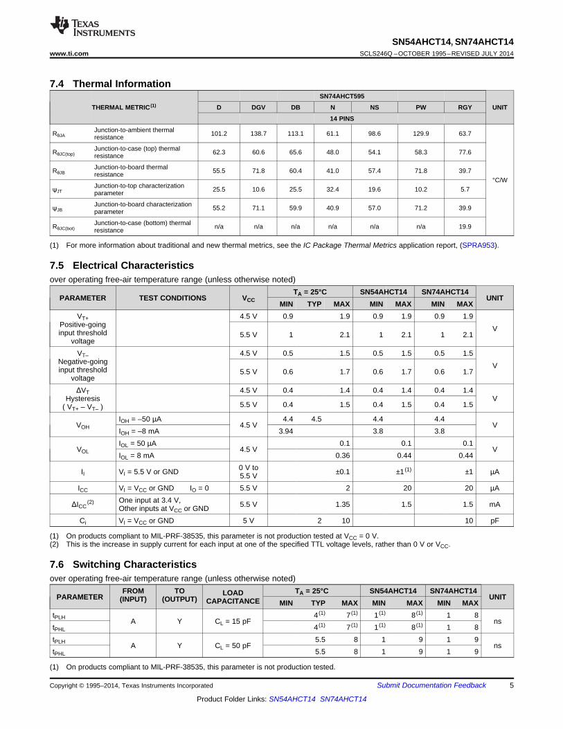
7.4 Thermal InformationSN74AHCT595
THERMAL METRIC (1) D DGV DB N NS PW RGY UNIT
14 PINS
Junction-to-ambient thermalRθJA 101.2 138.7 113.1 61.1 98.6 129.9 63.7resistance
Junction-to-case (top) thermalRθJC(top) 62.3 60.6 65.6 48.0 54.1 58.3 77.6resistance
Junction-to-board thermalRθJB 55.5 71.8 60.4 41.0 57.4 71.8 39.7resistance°C/W
Junction-to-top characterizationψJT 25.5 10.6 25.5 32.4 19.6 10.2 5.7parameter
Junction-to-board characterizationψJB 55.2 71.1 59.9 40.9 57.0 71.2 39.9parameter
Junction-to-case (bottom) thermalRθJC(bot) n/a n/a n/a n/a n/a n/a 19.9resistance
(1) For more information about traditional and new thermal metrics, see the IC Package Thermal Metrics application report, (SPRA953).
7.5 Electrical Characteristicsover operating free-air temperature range (unless otherwise noted)
TA = 25°C SN54AHCT14 SN74AHCT14PARAMETER TEST CONDITIONS VCC UNIT
MIN TYP MAX MIN MAX MIN MAXVT+ 4.5 V 0.9 1.9 0.9 1.9 0.9 1.9
Positive-going Vinput threshold 5.5 V 1 2.1 1 2.1 1 2.1voltage
VT– 4.5 V 0.5 1.5 0.5 1.5 0.5 1.5Negative-going Vinput threshold 5.5 V 0.6 1.7 0.6 1.7 0.6 1.7
voltageΔVT 4.5 V 0.4 1.4 0.4 1.4 0.4 1.4
Hysteresis V5.5 V 0.4 1.5 0.4 1.5 0.4 1.5( VT+ – VT– )
IOH = –50 µA 4.4 4.5 4.4 4.4VOH 4.5 V V
IOH = –8 mA 3.94 3.8 3.8IOL = 50 µA 0.1 0.1 0.1
VOL 4.5 V VIOL = 8 mA 0.36 0.44 0.44
0 V toII VI = 5.5 V or GND ±0.1 ±1 (1) ±1 µA5.5 VICC VI = VCC or GND IO = 0 5.5 V 2 20 20 µA
One input at 3.4 V,ΔICC(2) 5.5 V 1.35 1.5 1.5 mAOther inputs at VCC or GND
Ci VI = VCC or GND 5 V 2 10 10 pF
(1) On products compliant to MIL-PRF-38535, this parameter is not production tested at VCC = 0 V.(2) This is the increase in supply current for each input at one of the specified TTL voltage levels, rather than 0 V or VCC.
7.6 Switching Characteristicsover operating free-air temperature range (unless otherwise noted)
FROM TO TA = 25°C SN54AHCT14 SN74AHCT14LOADPARAMETER UNIT(INPUT) (OUTPUT) CAPACITANCE MIN TYP MAX MIN MAX MIN MAXtPLH 4 (1) 7 (1) 1 (1) 8 (1) 1 8
A Y CL = 15 pF nstPHL 4 (1) 7 (1) 1 (1) 8 (1) 1 8tPLH 5.5 8 1 9 1 9
A Y CL = 50 pF nstPHL 5.5 8 1 9 1 9
(1) On products compliant to MIL-PRF-38535, this parameter is not production tested.
Copyright © 1995–2014, Texas Instruments Incorporated Submit Documentation Feedback 5
Product Folder Links: SN54AHCT14 SN74AHCT14

SN54AHCT14, SN74AHCT14SCLS246Q –OCTOBER 1995–REVISED JULY 2014 www.ti.com
7.7 Noise CharacteristicsVCC = 5 V, CL = 50 pF, TA = 25°C (1)
SN74AHCT14PARAMETER UNIT
MIN TYP MAXVOL(P) Quiet output, maximum dynamic VOL 0.9 VVOL(V) Quiet output, minimum dynamic VOL –0.7 VVOH(V) Quiet output, minimum dynamic VOH 4.3 VVIH(D) High-level dynamic input voltage 2.1 VVIL(D) Low-level dynamic input voltage 0.5 V
(1) Characteristics are for surface-mount packages only.
7.8 Operating CharacteristicsVCC = 5 V, TA = 25°C
PARAMETER TEST CONDITIONS TYP UNITCpd Power dissipation capacitance No load, f = 1 MHz 112 pF
7.9 Typical CharacteristicsOne common misconception is that the current consumption will be less when switching a slow signal into a Schmitt trigger.This is partly true because the Schmitt trigger prevents oscillation which can draw a lot of current; however, you will seehigher ICC current due to the amount of time the input is not at the rail. This is Delta ICC. Delta ICC is where the inputs are notat the rails and upper or lower drive transistors are partially on. Figure 1 shows ICC across the input voltage sweep.
Figure 1. Supply Current vs Input Voltage
6 Submit Documentation Feedback Copyright © 1995–2014, Texas Instruments Incorporated
Product Folder Links: SN54AHCT14 SN74AHCT14

50% VCC
3 V
3 V
0 V
0 V
thtsu
VOLTAGE WAVEFORMS
SETUP AND HOLD TIMES
Data Input
tPLH
tPHL
tPHL
tPLH
VOH
VOH
VOL
VOL
3 V
0 V
50% VCC50% VCC
Input
Out-of-Phase
Output
In-Phase
Output
Timing Input
50% VCC
VOLTAGE WAVEFORMS
PROPAGATION DELAY TIMES
INVERTING AND NONINVERTING OUTPUTS
Output
Control
Output
Waveform 1
S1 at VCC
(see Note B)
Output
Waveform 2
S1 at GND
(see Note B)
VOL
VOH
tPZL
tPZH
tPLZ
tPHZ
≈VCC
0 V
50% VCCVOL + 0.3 V
50% VCC
≈0 V
3 V
VOLTAGE WAVEFORMS
ENABLE AND DISABLE TIMES
LOW- AND HIGH-LEVEL ENABLING
tPLH/tPHL
tPLZ/tPZL
tPHZ/tPZH
Open Drain
Open
VCC
GND
VCC
TEST S1
3 V
0 V
tw
VOLTAGE WAVEFORMS
PULSE DURATION
Input
NOTES: A. CL includes probe and jig capacitance.
B. Waveform 1 is for an output with internal conditions such that the output is low except when disabled by the output control.
Waveform 2 is for an output with internal conditions such that the output is high except when disabled by the output control.
C. All input pulses are supplied by generators having the following characteristics: PRR ≤ 1 MHz, ZO = 50 Ω, tr ≤ 3 ns, tf ≤ 3 ns.
D. The outputs are measured one at a time with one input transition per measurement.
E. All parameters and waveforms are not applicable to all devices.
From Output
Under Test
CL
(see Note A)
LOAD CIRCUIT FOR
3-STATE AND OPEN-DRAIN OUTPUTS
S1
VCC
RL = 1 kΩ
GNDFrom Output
Under Test
CL
(see Note A)
Test
Point
LOAD CIRCUIT FOR
TOTEM-POLE OUTPUTS
Open
VOH – 0.3 V
1.5 V 1.5 V
1.5 V
1.5 V 1.5 V
1.5 V 1.5 V1.5 V 1.5 V
SN54AHCT14, SN74AHCT14www.ti.com SCLS246Q –OCTOBER 1995–REVISED JULY 2014
8 Parameter Measurement Information
Figure 2. Load Circuit and Voltage Waveforms
Copyright © 1995–2014, Texas Instruments Incorporated Submit Documentation Feedback 7
Product Folder Links: SN54AHCT14 SN74AHCT14

YA
SN54AHCT14, SN74AHCT14SCLS246Q –OCTOBER 1995–REVISED JULY 2014 www.ti.com
9 Detailed Description
9.1 OverviewThe SNx4AHCT14 devices contain six independent inverters. These devices perform the Boolean function Y = A.Each circuit functions as an independent inverter, but because of the Schmitt action, the inverters have differentinput threshold levels for positive-going (VT+) and for negative-going (VT−) signals.
9.2 Functional Block Diagram
9.3 Feature Description• Inputs are TTL-Voltage compatible• Inputs accept very slow or noisy inputs
9.4 Device Functional Modes
Table 1. Function Table(Each Inverter)
INPUT OUTPUTA YH LL H
8 Submit Documentation Feedback Copyright © 1995–2014, Texas Instruments Incorporated
Product Folder Links: SN54AHCT14 SN74AHCT14

5 V
10 kΩ 1/6 WSN74AHCT14
10 nf
Circuit Symbol for a
Schmitt Trigger
SN54AHCT14, SN74AHCT14www.ti.com SCLS246Q –OCTOBER 1995–REVISED JULY 2014
10 Application and Implementation
10.1 Application InformationSchmitt triggers should be used anytime you need to translate a sign wave into a square wave, or used where aslow or noisy input needs to be sped up or cleaned up as in the switch de-bouncer circuit.
10.2 Typical Application
Figure 3. Switch De-bouncer Using Schmitt Trigger Inverter
10.2.1 Design RequirementsThis device uses CMOS technology and has balanced output drive. Care should be taken to avoid buscontention because it can drive currents that would exceed maximum limits. The high drive will also create fastedges into light loads; therefore, routing and load conditions should be considered to prevent ringing.
10.2.2 Detailed Design Procedure1. Recommended input conditions
– Rise time and fall time specs: See (Δt/ΔV) in the Recommended Operating Conditions table.– Specified High and low levels: See (VIH and VIL) in the Recommended Operating Conditions table.– Inputs are overvoltage tolerant allowing them to go as high as 5.5 V at any valid VCC
2. Recommend output conditions– Load currents should not exceed 25 mA per output and 50 mA total for the part– Outputs should not be pulled above VCC
Copyright © 1995–2014, Texas Instruments Incorporated Submit Documentation Feedback 9
Product Folder Links: SN54AHCT14 SN74AHCT14

SN54AHCT14, SN74AHCT14SCLS246Q –OCTOBER 1995–REVISED JULY 2014 www.ti.com
Typical Application (continued)10.2.3 Application Curves
Figure 4. Typical Application Curves
10 Submit Documentation Feedback Copyright © 1995–2014, Texas Instruments Incorporated
Product Folder Links: SN54AHCT14 SN74AHCT14

Vcc
Unused Input
Input
Output
Input
Unused Input Output
SN54AHCT14, SN74AHCT14www.ti.com SCLS246Q –OCTOBER 1995–REVISED JULY 2014
11 Power Supply RecommendationsThe power supply can be any voltage between the MIN and MAX supply voltage rating located in theRecommended Operating Conditions table.
Each VCC pin should have a good bypass capacitor to prevent power disturbance. For devices with a singlesupply, 0.1 μf is recommended. If there are multiple VCC pins, 0.01 μf or 0.022 μf is recommended for eachpower pin. It is acceptable to parallel multiple bypass caps to reject different frequencies of noise. A 0.1 μf and 1μf are commonly used in parallel. The bypass capacitor should be installed as close to the power pin as possiblefor best results.
12 Layout
12.1 Layout GuidelinesWhen using multiple bit logic devices inputs should not ever float.
In many cases, functions or parts of functions of digital logic devices are unused, for example, when only twoinputs of a triple-input AND gate are used or only 3 of the 4 buffer gates are used. Such input pins should not beleft unconnected because the undefined voltages at the outside connections result in undefined operationalstates. Specified in Figure 5 are the rules that must be observed under all circumstances. All unused inputs ofdigital logic devices must be connected to a high or low bias to prevent them from floating. The logic level thatshould be applied to any particular unused input depends on the function of the device. Generally they will betied to GND or VCC; whichever makes more sense or is more convenient. It is generally acceptable to floatoutputs unless the part is a transceiver. If the transceiver has an output enable pin, it will disable the outputssection of the part when asserted. This will not disable the input section of the IO’s so they cannot float whendisabled.
12.2 Layout Example
Figure 5. Layout Diagram
Copyright © 1995–2014, Texas Instruments Incorporated Submit Documentation Feedback 11
Product Folder Links: SN54AHCT14 SN74AHCT14

SN54AHCT14, SN74AHCT14SCLS246Q –OCTOBER 1995–REVISED JULY 2014 www.ti.com
13 Device and Documentation Support
13.1 Related LinksThe table below lists quick access links. Categories include technical documents, support and communityresources, tools and software, and quick access to sample or buy.
Table 2. Related LinksTECHNICAL TOOLS & SUPPORT &PARTS PRODUCT FOLDER SAMPLE & BUY DOCUMENTS SOFTWARE COMMUNITY
SN54AHCT14 Click here Click here Click here Click here Click hereSN74AHCT14 Click here Click here Click here Click here Click here
13.2 Trademarks
13.3 Electrostatic Discharge CautionThese devices have limited built-in ESD protection. The leads should be shorted together or the device placed in conductive foamduring storage or handling to prevent electrostatic damage to the MOS gates.
13.4 GlossarySLYZ022 — TI Glossary.
This glossary lists and explains terms, acronyms, and definitions.
14 Mechanical, Packaging, and Orderable InformationThe following pages include mechanical, packaging, and orderable information. This information is the mostcurrent data available for the designated devices. This data is subject to change without notice and revision ofthis document. For browser-based versions of this data sheet, refer to the left-hand navigation.
12 Submit Documentation Feedback Copyright © 1995–2014, Texas Instruments Incorporated
Product Folder Links: SN54AHCT14 SN74AHCT14

PACKAGE OPTION ADDENDUM
www.ti.com 24-Aug-2018
Addendum-Page 1
PACKAGING INFORMATION
Orderable Device Status(1)
Package Type PackageDrawing
Pins PackageQty
Eco Plan(2)
Lead/Ball Finish(6)
MSL Peak Temp(3)
Op Temp (°C) Device Marking(4/5)
Samples
5962-9680101Q2A ACTIVE LCCC FK 20 1 TBD POST-PLATE N / A for Pkg Type -55 to 125 5962-9680101Q2ASNJ54AHCT14FK
5962-9680101QCA ACTIVE CDIP J 14 1 TBD A42 N / A for Pkg Type -55 to 125 5962-9680101QCASNJ54AHCT14J
5962-9680101QDA ACTIVE CFP W 14 1 TBD A42 N / A for Pkg Type -55 to 125 5962-9680101QDASNJ54AHCT14W
5962-9680101VCA ACTIVE CDIP J 14 1 TBD A42 N / A for Pkg Type -55 to 125 5962-9680101VCASNV54AHCT14J
5962-9680101VDA ACTIVE CFP W 14 1 TBD A42 N / A for Pkg Type -55 to 125 5962-9680101VDASNV54AHCT14W
SN74AHCT14D ACTIVE SOIC D 14 50 Green (RoHS& no Sb/Br)
CU NIPDAU Level-1-260C-UNLIM -40 to 85 AHCT14
SN74AHCT14DBR ACTIVE SSOP DB 14 2000 Green (RoHS& no Sb/Br)
CU NIPDAU Level-1-260C-UNLIM -40 to 85 HB14
SN74AHCT14DG4 ACTIVE SOIC D 14 50 Green (RoHS& no Sb/Br)
CU NIPDAU Level-1-260C-UNLIM -40 to 85 AHCT14
SN74AHCT14DGVR ACTIVE TVSOP DGV 14 2000 Green (RoHS& no Sb/Br)
CU NIPDAU Level-1-260C-UNLIM -40 to 85 HB14
SN74AHCT14DGVRE4 ACTIVE TVSOP DGV 14 2000 Green (RoHS& no Sb/Br)
CU NIPDAU Level-1-260C-UNLIM -40 to 85 HB14
SN74AHCT14DR ACTIVE SOIC D 14 2500 Green (RoHS& no Sb/Br)
CU NIPDAU Level-1-260C-UNLIM -40 to 85 AHCT14
SN74AHCT14DRG4 ACTIVE SOIC D 14 2500 Green (RoHS& no Sb/Br)
CU NIPDAU Level-1-260C-UNLIM -40 to 85 AHCT14
SN74AHCT14N ACTIVE PDIP N 14 25 Green (RoHS& no Sb/Br)
CU NIPDAU N / A for Pkg Type -40 to 85 SN74AHCT14N
SN74AHCT14NSR ACTIVE SO NS 14 2000 Green (RoHS& no Sb/Br)
CU NIPDAU Level-1-260C-UNLIM -40 to 85 AHCT14

PACKAGE OPTION ADDENDUM
www.ti.com 24-Aug-2018
Addendum-Page 2
Orderable Device Status(1)
Package Type PackageDrawing
Pins PackageQty
Eco Plan(2)
Lead/Ball Finish(6)
MSL Peak Temp(3)
Op Temp (°C) Device Marking(4/5)
Samples
SN74AHCT14PW ACTIVE TSSOP PW 14 90 Green (RoHS& no Sb/Br)
CU NIPDAU Level-1-260C-UNLIM -40 to 85 HB14
SN74AHCT14PWE4 ACTIVE TSSOP PW 14 90 Green (RoHS& no Sb/Br)
CU NIPDAU Level-1-260C-UNLIM -40 to 85 HB14
SN74AHCT14PWR ACTIVE TSSOP PW 14 2000 Green (RoHS& no Sb/Br)
CU NIPDAU Level-1-260C-UNLIM -40 to 85 HB14
SN74AHCT14PWRE4 ACTIVE TSSOP PW 14 2000 Green (RoHS& no Sb/Br)
CU NIPDAU Level-1-260C-UNLIM -40 to 85 HB14
SN74AHCT14RGYR ACTIVE VQFN RGY 14 3000 Green (RoHS& no Sb/Br)
CU NIPDAU Level-2-260C-1 YEAR -40 to 85 HB14
SNJ54AHCT14FK ACTIVE LCCC FK 20 1 TBD POST-PLATE N / A for Pkg Type -55 to 125 5962-9680101Q2ASNJ54AHCT14FK
SNJ54AHCT14J ACTIVE CDIP J 14 1 TBD A42 N / A for Pkg Type -55 to 125 5962-9680101QCASNJ54AHCT14J
SNJ54AHCT14W ACTIVE CFP W 14 1 TBD A42 N / A for Pkg Type -55 to 125 5962-9680101QDASNJ54AHCT14W
(1) The marketing status values are defined as follows:ACTIVE: Product device recommended for new designs.LIFEBUY: TI has announced that the device will be discontinued, and a lifetime-buy period is in effect.NRND: Not recommended for new designs. Device is in production to support existing customers, but TI does not recommend using this part in a new design.PREVIEW: Device has been announced but is not in production. Samples may or may not be available.OBSOLETE: TI has discontinued the production of the device.
(2) RoHS: TI defines "RoHS" to mean semiconductor products that are compliant with the current EU RoHS requirements for all 10 RoHS substances, including the requirement that RoHS substancedo not exceed 0.1% by weight in homogeneous materials. Where designed to be soldered at high temperatures, "RoHS" products are suitable for use in specified lead-free processes. TI mayreference these types of products as "Pb-Free".RoHS Exempt: TI defines "RoHS Exempt" to mean products that contain lead but are compliant with EU RoHS pursuant to a specific EU RoHS exemption.Green: TI defines "Green" to mean the content of Chlorine (Cl) and Bromine (Br) based flame retardants meet JS709B low halogen requirements of <=1000ppm threshold. Antimony trioxide basedflame retardants must also meet the <=1000ppm threshold requirement.
(3) MSL, Peak Temp. - The Moisture Sensitivity Level rating according to the JEDEC industry standard classifications, and peak solder temperature.
(4) There may be additional marking, which relates to the logo, the lot trace code information, or the environmental category on the device.

PACKAGE OPTION ADDENDUM
www.ti.com 24-Aug-2018
Addendum-Page 3
(5) Multiple Device Markings will be inside parentheses. Only one Device Marking contained in parentheses and separated by a "~" will appear on a device. If a line is indented then it is a continuationof the previous line and the two combined represent the entire Device Marking for that device.
(6) Lead/Ball Finish - Orderable Devices may have multiple material finish options. Finish options are separated by a vertical ruled line. Lead/Ball Finish values may wrap to two lines if the finishvalue exceeds the maximum column width.
Important Information and Disclaimer:The information provided on this page represents TI's knowledge and belief as of the date that it is provided. TI bases its knowledge and belief on informationprovided by third parties, and makes no representation or warranty as to the accuracy of such information. Efforts are underway to better integrate information from third parties. TI has taken andcontinues to take reasonable steps to provide representative and accurate information but may not have conducted destructive testing or chemical analysis on incoming materials and chemicals.TI and TI suppliers consider certain information to be proprietary, and thus CAS numbers and other limited information may not be available for release.
In no event shall TI's liability arising out of such information exceed the total purchase price of the TI part(s) at issue in this document sold by TI to Customer on an annual basis.
OTHER QUALIFIED VERSIONS OF SN54AHCT14, SN54AHCT14-SP, SN74AHCT14 :
• Catalog: SN74AHCT14, SN54AHCT14
• Enhanced Product: SN74AHCT14-EP, SN74AHCT14-EP
• Military: SN54AHCT14
• Space: SN54AHCT14-SP
NOTE: Qualified Version Definitions:
• Catalog - TI's standard catalog product
• Enhanced Product - Supports Defense, Aerospace and Medical Applications
• Military - QML certified for Military and Defense Applications
• Space - Radiation tolerant, ceramic packaging and qualified for use in Space-based application

TAPE AND REEL INFORMATION
*All dimensions are nominal
Device PackageType
PackageDrawing
Pins SPQ ReelDiameter
(mm)
ReelWidth
W1 (mm)
A0(mm)
B0(mm)
K0(mm)
P1(mm)
W(mm)
Pin1Quadrant
SN74AHCT14DBR SSOP DB 14 2000 330.0 16.4 8.2 6.6 2.5 12.0 16.0 Q1
SN74AHCT14DGVR TVSOP DGV 14 2000 330.0 12.4 6.8 4.0 1.6 8.0 12.0 Q1
SN74AHCT14DR SOIC D 14 2500 330.0 16.4 6.5 9.0 2.1 8.0 16.0 Q1
SN74AHCT14NSR SO NS 14 2000 330.0 16.4 8.2 10.5 2.5 12.0 16.0 Q1
SN74AHCT14PWR TSSOP PW 14 2000 330.0 12.4 6.9 5.6 1.6 8.0 12.0 Q1
SN74AHCT14RGYR VQFN RGY 14 3000 330.0 12.4 3.75 3.75 1.15 8.0 12.0 Q1
PACKAGE MATERIALS INFORMATION
www.ti.com 30-Jun-2014
Pack Materials-Page 1

*All dimensions are nominal
Device Package Type Package Drawing Pins SPQ Length (mm) Width (mm) Height (mm)
SN74AHCT14DBR SSOP DB 14 2000 367.0 367.0 38.0
SN74AHCT14DGVR TVSOP DGV 14 2000 367.0 367.0 35.0
SN74AHCT14DR SOIC D 14 2500 367.0 367.0 38.0
SN74AHCT14NSR SO NS 14 2000 367.0 367.0 38.0
SN74AHCT14PWR TSSOP PW 14 2000 367.0 367.0 35.0
SN74AHCT14RGYR VQFN RGY 14 3000 367.0 367.0 35.0
PACKAGE MATERIALS INFORMATION
www.ti.com 30-Jun-2014
Pack Materials-Page 2


MECHANICAL DATA
MPDS006C – FEBRUARY 1996 – REVISED AUGUST 2000
POST OFFICE BOX 655303 • DALLAS, TEXAS 75265
DGV (R-PDSO-G**) PLASTIC SMALL-OUTLINE 24 PINS SHOWN
14
3,70
3,50 4,90
5,10
20DIM
PINS **
4073251/E 08/00
1,20 MAX
Seating Plane
0,050,15
0,25
0,500,75
0,230,13
1 12
24 13
4,304,50
0,16 NOM
Gage Plane
A
7,90
7,70
382416
4,90
5,103,70
3,50
A MAX
A MIN
6,606,20
11,20
11,40
56
9,60
9,80
48
0,08
M0,070,40
0°–8°
NOTES: A. All linear dimensions are in millimeters.B. This drawing is subject to change without notice.C. Body dimensions do not include mold flash or protrusion, not to exceed 0,15 per side.D. Falls within JEDEC: 24/48 Pins – MO-153
14/16/20/56 Pins – MO-194


www.ti.com
PACKAGE OUTLINE
C
14X .008-.014 [0.2-0.36]TYP
-150
AT GAGE PLANE
-.314.308-7.977.83[ ]
14X -.026.014-0.660.36[ ]14X -.065.045
-1.651.15[ ]
.2 MAX TYP[5.08]
.13 MIN TYP[3.3]
TYP-.060.015-1.520.38[ ]
4X .005 MIN[0.13]
12X .100[2.54]
.015 GAGE PLANE[0.38]
A
-.785.754-19.9419.15[ ]
B -.283.245-7.196.22[ ]
CDIP - 5.08 mm max heightJ0014ACERAMIC DUAL IN LINE PACKAGE
4214771/A 05/2017
NOTES: 1. All controlling linear dimensions are in inches. Dimensions in brackets are in millimeters. Any dimension in brackets or parenthesis are for reference only. Dimensioning and tolerancing per ASME Y14.5M.2. This drawing is subject to change without notice. 3. This package is hermitically sealed with a ceramic lid using glass frit.4. Index point is provided on cap for terminal identification only and on press ceramic glass frit seal only.5. Falls within MIL-STD-1835 and GDIP1-T14.
7 8
141
PIN 1 ID(OPTIONAL)
SCALE 0.900
SEATING PLANE
.010 [0.25] C A B

www.ti.com
EXAMPLE BOARD LAYOUT
ALL AROUND[0.05]
MAX.002
.002 MAX[0.05]ALL AROUND
SOLDER MASKOPENING
METAL
(.063)[1.6]
(R.002 ) TYP[0.05]
14X ( .039)[1]
( .063)[1.6]
12X (.100 )[2.54]
(.300 ) TYP[7.62]
CDIP - 5.08 mm max heightJ0014ACERAMIC DUAL IN LINE PACKAGE
4214771/A 05/2017
LAND PATTERN EXAMPLENON-SOLDER MASK DEFINED
SCALE: 5X
SEE DETAIL A SEE DETAIL B
SYMM
SYMM
1
7 8
14
DETAIL ASCALE: 15X
SOLDER MASKOPENING
METAL
DETAIL B13X, SCALE: 15X


MECHANICAL DATA
MSSO002E – JANUARY 1995 – REVISED DECEMBER 2001
POST OFFICE BOX 655303 • DALLAS, TEXAS 75265
DB (R-PDSO-G**) PLASTIC SMALL-OUTLINE
4040065 /E 12/01
28 PINS SHOWN
Gage Plane
8,207,40
0,550,95
0,25
38
12,90
12,30
28
10,50
24
8,50
Seating Plane
9,907,90
30
10,50
9,90
0,38
5,605,00
15
0,22
14
A
28
1
2016
6,506,50
14
0,05 MIN
5,905,90
DIM
A MAX
A MIN
PINS **
2,00 MAX
6,90
7,50
0,65 M0,15
0°–8°
0,10
0,090,25
NOTES: A. All linear dimensions are in millimeters.B. This drawing is subject to change without notice.C. Body dimensions do not include mold flash or protrusion not to exceed 0,15.D. Falls within JEDEC MO-150

IMPORTANT NOTICE
Texas Instruments Incorporated (TI) reserves the right to make corrections, enhancements, improvements and other changes to itssemiconductor products and services per JESD46, latest issue, and to discontinue any product or service per JESD48, latest issue. Buyersshould obtain the latest relevant information before placing orders and should verify that such information is current and complete.TI’s published terms of sale for semiconductor products (http://www.ti.com/sc/docs/stdterms.htm) apply to the sale of packaged integratedcircuit products that TI has qualified and released to market. Additional terms may apply to the use or sale of other types of TI products andservices.Reproduction of significant portions of TI information in TI data sheets is permissible only if reproduction is without alteration and isaccompanied by all associated warranties, conditions, limitations, and notices. TI is not responsible or liable for such reproduceddocumentation. Information of third parties may be subject to additional restrictions. Resale of TI products or services with statementsdifferent from or beyond the parameters stated by TI for that product or service voids all express and any implied warranties for theassociated TI product or service and is an unfair and deceptive business practice. TI is not responsible or liable for any such statements.Buyers and others who are developing systems that incorporate TI products (collectively, “Designers”) understand and agree that Designersremain responsible for using their independent analysis, evaluation and judgment in designing their applications and that Designers havefull and exclusive responsibility to assure the safety of Designers' applications and compliance of their applications (and of all TI productsused in or for Designers’ applications) with all applicable regulations, laws and other applicable requirements. Designer represents that, withrespect to their applications, Designer has all the necessary expertise to create and implement safeguards that (1) anticipate dangerousconsequences of failures, (2) monitor failures and their consequences, and (3) lessen the likelihood of failures that might cause harm andtake appropriate actions. Designer agrees that prior to using or distributing any applications that include TI products, Designer willthoroughly test such applications and the functionality of such TI products as used in such applications.TI’s provision of technical, application or other design advice, quality characterization, reliability data or other services or information,including, but not limited to, reference designs and materials relating to evaluation modules, (collectively, “TI Resources”) are intended toassist designers who are developing applications that incorporate TI products; by downloading, accessing or using TI Resources in anyway, Designer (individually or, if Designer is acting on behalf of a company, Designer’s company) agrees to use any particular TI Resourcesolely for this purpose and subject to the terms of this Notice.TI’s provision of TI Resources does not expand or otherwise alter TI’s applicable published warranties or warranty disclaimers for TIproducts, and no additional obligations or liabilities arise from TI providing such TI Resources. TI reserves the right to make corrections,enhancements, improvements and other changes to its TI Resources. TI has not conducted any testing other than that specificallydescribed in the published documentation for a particular TI Resource.Designer is authorized to use, copy and modify any individual TI Resource only in connection with the development of applications thatinclude the TI product(s) identified in such TI Resource. NO OTHER LICENSE, EXPRESS OR IMPLIED, BY ESTOPPEL OR OTHERWISETO ANY OTHER TI INTELLECTUAL PROPERTY RIGHT, AND NO LICENSE TO ANY TECHNOLOGY OR INTELLECTUAL PROPERTYRIGHT OF TI OR ANY THIRD PARTY IS GRANTED HEREIN, including but not limited to any patent right, copyright, mask work right, orother intellectual property right relating to any combination, machine, or process in which TI products or services are used. Informationregarding or referencing third-party products or services does not constitute a license to use such products or services, or a warranty orendorsement thereof. Use of TI Resources may require a license from a third party under the patents or other intellectual property of thethird party, or a license from TI under the patents or other intellectual property of TI.TI RESOURCES ARE PROVIDED “AS IS” AND WITH ALL FAULTS. TI DISCLAIMS ALL OTHER WARRANTIES ORREPRESENTATIONS, EXPRESS OR IMPLIED, REGARDING RESOURCES OR USE THEREOF, INCLUDING BUT NOT LIMITED TOACCURACY OR COMPLETENESS, TITLE, ANY EPIDEMIC FAILURE WARRANTY AND ANY IMPLIED WARRANTIES OFMERCHANTABILITY, FITNESS FOR A PARTICULAR PURPOSE, AND NON-INFRINGEMENT OF ANY THIRD PARTY INTELLECTUALPROPERTY RIGHTS. TI SHALL NOT BE LIABLE FOR AND SHALL NOT DEFEND OR INDEMNIFY DESIGNER AGAINST ANY CLAIM,INCLUDING BUT NOT LIMITED TO ANY INFRINGEMENT CLAIM THAT RELATES TO OR IS BASED ON ANY COMBINATION OFPRODUCTS EVEN IF DESCRIBED IN TI RESOURCES OR OTHERWISE. IN NO EVENT SHALL TI BE LIABLE FOR ANY ACTUAL,DIRECT, SPECIAL, COLLATERAL, INDIRECT, PUNITIVE, INCIDENTAL, CONSEQUENTIAL OR EXEMPLARY DAMAGES INCONNECTION WITH OR ARISING OUT OF TI RESOURCES OR USE THEREOF, AND REGARDLESS OF WHETHER TI HAS BEENADVISED OF THE POSSIBILITY OF SUCH DAMAGES.Unless TI has explicitly designated an individual product as meeting the requirements of a particular industry standard (e.g., ISO/TS 16949and ISO 26262), TI is not responsible for any failure to meet such industry standard requirements.Where TI specifically promotes products as facilitating functional safety or as compliant with industry functional safety standards, suchproducts are intended to help enable customers to design and create their own applications that meet applicable functional safety standardsand requirements. Using products in an application does not by itself establish any safety features in the application. Designers mustensure compliance with safety-related requirements and standards applicable to their applications. Designer may not use any TI products inlife-critical medical equipment unless authorized officers of the parties have executed a special contract specifically governing such use.Life-critical medical equipment is medical equipment where failure of such equipment would cause serious bodily injury or death (e.g., lifesupport, pacemakers, defibrillators, heart pumps, neurostimulators, and implantables). Such equipment includes, without limitation, allmedical devices identified by the U.S. Food and Drug Administration as Class III devices and equivalent classifications outside the U.S.TI may expressly designate certain products as completing a particular qualification (e.g., Q100, Military Grade, or Enhanced Product).Designers agree that it has the necessary expertise to select the product with the appropriate qualification designation for their applicationsand that proper product selection is at Designers’ own risk. Designers are solely responsible for compliance with all legal and regulatoryrequirements in connection with such selection.Designer will fully indemnify TI and its representatives against any damages, costs, losses, and/or liabilities arising out of Designer’s non-compliance with the terms and provisions of this Notice.
Mailing Address: Texas Instruments, Post Office Box 655303, Dallas, Texas 75265Copyright © 2018, Texas Instruments Incorporated