sn74s1053 16-bit schottky barrier diode … · sn74s1053 16-bit schottky barrier diode...
TRANSCRIPT

SN74S105316-BIT SCHOTTKY BARRIER DIODE
BUS-TERMINATION ARRAY
SDLS017A – SEPTEMBER 1990 – REVISED AUGUST 1997
1POST OFFICE BOX 655303 • DALLAS, TEXAS 75265
Designed to Reduce Reflection Noise
Repetitive Peak Forward Current to 200 mA
16-Bit Array Structure Suited forBus-Oriented Systems
Package Options Include PlasticSmall-Outline Packages and StandardPlastic 300-mil DIPs
description
This Schottky barrier diode bus-termination arrayis designed to reduce reflection noise on memorybus lines. This device consists of a 16-bithigh-speed Schottky diode array suitable forclamping to VCC and/or GND.
The SN74S1053 is characterized for operationfrom 0°C to 70°C.
schematic diagrams
D012
D023
D034
D045
D056
D067
D078
D089
D0912
D1013
D1114
D1215
D1316
D1417
D1518
D1619
10GND
11GND
VCC1
VCC20
Copyright 1997, Texas Instruments IncorporatedPRODUCTION DATA information is current as of publication date.Products conform to specifications per the terms of Texas Instrumentsstandard warranty. Production processing does not necessarily includetesting of all parameters.
Please be aware that an important notice concerning availability, standard warranty, and use in critical applications ofTexas Instruments semiconductor products and disclaimers thereto appears at the end of this data sheet.
1
2
3
4
5
6
7
8
9
10
20
19
18
17
16
15
14
13
12
11
VCCD01D02D03D04D05D06D07D08
GND
VCCD16D15D14D13D12D11D10D09GND
DW OR N PACKAGE(TOP VIEW)

SN74S105316-BIT SCHOTTKY BARRIER DIODEBUS-TERMINATION ARRAY
SDLS017A – SEPTEMBER 1990 – REVISED AUGUST 1997
2 POST OFFICE BOX 655303 • DALLAS, TEXAS 75265
absolute maximum ratings over operating free-air temperature range (unless otherwise noted) †
Steady-state reverse voltage, VR 7 V. . . . . . . . . . . . . . . . . . . . . . . . . . . . . . . . . . . . . . . . . . . . . . . . . . . . . . . . . . . . . Continuous forward current, IF: Any D terminal from GND or to VCC 50 mA. . . . . . . . . . . . . . . . . . . . . . . . . . .
Total through all GND or VCC terminals 170 mA. . . . . . . . . . . . . . . . . . . . . . . Repetitive peak forward current‡, IFRM: Any D terminal from GND or VCC 200 mA. . . . . . . . . . . . . . . . . . . . .
Total through all GND or VCC terminals 1.2 A. . . . . . . . . . . . . . . . . . Continuous total power dissipation at (or below) 25°C free-air temperature (see Note 1) 625 mW. . . . . . . . . . Operating free-air temperature range 0°C to 70°C. . . . . . . . . . . . . . . . . . . . . . . . . . . . . . . . . . . . . . . . . . . . . . . . . . Storage temperature range, Tstg –65°C to 150°C. . . . . . . . . . . . . . . . . . . . . . . . . . . . . . . . . . . . . . . . . . . . . . . . . . .
† Stresses beyond those listed under “absolute maximum ratings” may cause permanent damage to the device. These are stress ratings only, andfunctional operation of the device at these or any other conditions beyond those indicated under “recommended operating conditions” is notimplied. Exposure to absolute-maximum-rated conditions for extended periods may affect device reliability.
‡ These values apply for tw ≤ 100 µs, duty cycle ≤ 20%.NOTE 1: For operation above 25°C free-air temperature, derate linearly at the rate of 5 m/W/°C.
electrical characteristics over recommended operating free-air temperature range (unlessotherwise noted)
single-diode operation (see Note 2)PARAMETER TEST CONDITIONS MIN TYP§ MAX UNIT
To VCCIF = 18 mA 0.85 1.05
VF Static forward voltage
To VCCIF = 50 mA 1.05 1.3
VVF Static forward voltage
From GNDIF = 18 mA 0.75 0.95
V
From GNDIF = 50 mA 0.95 1.2
VFM Peak forward voltage IF = 200 mA 1.45 V
IR Static reverse currentTo VCC
VR = 7 V5
µAIR Static reverse currentFrom GND
VR = 7 V5
µA
Ct Total capacitanceVR = 0 V, f = 1 MHz 8 16
pFCt Total capacitanceVR = 2 V, f = 1 MHz 4 8
pF
§ All typical values are at VCC = 5 V, TA = 25°C.NOTE 2: Test conditions and limits apply separately to each of the diodes. The diodes not under test are open-circuited during the measurement
of these characteristics.
multiple-diode operationPARAMETER TEST CONDITIONS MIN TYP‡ MAX UNIT
I Internal crosstalk currentTotal IF current = 1 A, See Note 3 0.8 2
mAIx Internal crosstalk currentTotal IF current = 198 mA, See Note 3 0.02 0.2
mA
§ All typical values are at VCC = 5 V, TA = 25°C.NOTE 3: Ix is measured under the following conditions with one diode static, and all others switching:
Switching diodes: tw = 100 µs, duty cycle = 20%Static diode: VR = 5 VThe static diode input current is the internal crosstalk current Ix.
switching characteristics, T A = 25°C (see Figures 1 and 2)
PARAMETER TEST CONDITIONS MIN TYP MAX UNIT
trr Reverse recovery time IF = 10 mA, IRM(REC) = 10 mA, IR(REC) = 1 mA, RL = 100 Ω 8 16 ns

SN74S105316-BIT SCHOTTKY BARRIER DIODE
BUS-TERMINATION ARRAY
SDLS017A – SEPTEMBER 1990 – REVISED AUGUST 1997
3POST OFFICE BOX 655303 • DALLAS, TEXAS 75265
PARAMETER MEASUREMENT INFORMATION
90%
10%
DUT
tr
VFM
(See Note A) (See Note B)
50 Ω 450 Ω
PulseGenerator
VF
SamplingOscilloscope
Input Pulse(See Note A)
OutputWaveform
(See Note B)
NOTES: A. The input pulse is supplied by a pulse generator having the following characteristics: tr = 20 ns, ZO = 50 Ω, freq = 500 Hz,duty cycle = 1%.
B. The output waveform is monitored by an oscilloscope having the following characteristics: tr ≤ 350 ps, Ri = 50 Ω, Ci ≤ 5 pF.
Figure 1. Forward Recovery Voltage
IF
DUT
90%
10%
tf If
PulseGenerator
(See Note A) (See Note B)
IR(REC)
trr
IRM(REC)
SamplingOscilloscope
Input Pulse(See Note A)
OutputWaveform
(See Note B)
0
NOTES: A. The input pulse is supplied by a pulse generator having the following characteristics: tf = 0.5 ns, ZO = 50 Ω, tw ≥ 50 ns,duty cycle = 1%.
B. The output waveform is monitored by an oscilloscope having the following characteristics: tr ≤ 350 ps, Ri = 50 Ω, Ci ≤ 5 pF.
Figure 2. Reverse Recovery Time

SN74S105316-BIT SCHOTTKY BARRIER DIODEBUS-TERMINATION ARRAY
SDLS017A – SEPTEMBER 1990 – REVISED AUGUST 1997
4 POST OFFICE BOX 655303 • DALLAS, TEXAS 75265
APPLICATION INFORMATION
Large negative transients occurring at the inputs of memory devices (DRAMs, SRAMs, EPROMs, etc.) or on theCLOCK lines of many clocked devices can result in improper operation of the devices. The SN74S1053 diodetermination array helps suppress negative transients caused by transmission-line reflections, crosstalk, andswitching noise.
Diode terminations have several advantages when compared to resistor termination schemes. Split resistor orThevenin equivalent termination can cause a substantial increase in power consumption. The use of a single resistorto ground to terminate a line usually results in degradation of the output high level, resulting in reduced noise immunity.Series damping resistors placed on the outputs of the driver reduce negative transients, but they also can increasepropagation delays down the line, as a series resistor reduces the output drive capability of the driving device. Diodeterminations have none of these drawbacks.
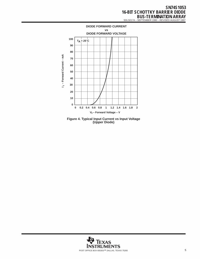
The operation of the diode arrays in reducing negative transients is explained in the following figures. The diodeconducts current when the voltage reaches a negative value large enough for the diode to turn on. Suppression ofnegative transients is tracked by the current-voltage characteristic curve for that diode. Typical current versus voltagecurves for the SN74S1053 are shown in Figures 3 and 4.
To illustrate how the diode arrays act to reduce negative transients at the end of a transmission line, the test setupin Figure 5 was evaluated. The resulting waveforms with and without the diode are shown in Figure 6.
The maximum effectiveness of the diode arrays in suppressing negative transients occurs when the diode arrays areplaced at the end of a line and/or the end of a long stub branching off a main transmission line. The diodes also canbe used to reduce the negative transients that occur due to discontinuities in the middle of a line. An example of thisis a slot in a backplane that is provided for an add-on card.
– F
orw
ard
Cur
rent
– m
A
VI – Forward Voltage – V
I I
DIODE FORWARD CURRENTvs
DIODE FORWARD VOLTAGE
–50
–40
–20
–10
0
–90
–30
0 0.2 0.4 0.6 0.8 1 1.2
–70
–60
–80
–100
1.4 1.6 1.8 2
TA = 25°C
Figure 3. Typical Input Current vs Input Voltage(Lower Diode)
SN74S105316-BIT SCHOTTKY BARRIER DIODE
BUS-TERMINATION ARRAY
SDLS017A – SEPTEMBER 1990 – REVISED AUGUST 1997
5POST OFFICE BOX 655303 • DALLAS, TEXAS 75265
– F
orw
ard
Cur
rent
– m
A
VI – Forward Voltage – V
I I
DIODE FORWARD CURRENTvs
DIODE FORWARD VOLTAGE
50
40
20
10
0
90
30
0 0.2 0.4 0.6 0.8 1 1.2
70
60
80
100
1.4 1.6 1.8 2
TA = 25°C
Figure 4. Typical Input Current vs Input Voltage(Upper Diode)

SN74S105316-BIT SCHOTTKY BARRIER DIODEBUS-TERMINATION ARRAY
SDLS017A – SEPTEMBER 1990 – REVISED AUGUST 1997
6 POST OFFICE BOX 655303 • DALLAS, TEXAS 75265
APPLICATION INFORMATION
ZO = 50 ΩLength = 36 in.
Figure 5. Diode Test Setup
31.500 ns
Ch 2 = 1.880 V/divTimebase = 5.00 ns/VMemory 1 = 1.880 V/divVmarker 1 = –1.353 VVmarker 2 = –3.647 V
Offset = 0.000 VDelay = 56.500 nsDelta V = –2.293 V
56.500 ns 81.500 ns
End-of-Line With DiodeEnd-of-
LineWithout
Diode
Vmarker 1
Vmarker 2
Figure 6. Oscilloscope Display

PACKAGE OPTION ADDENDUM
www.ti.com 10-Jun-2014
Addendum-Page 1
PACKAGING INFORMATION
Orderable Device Status(1)
Package Type PackageDrawing
Pins PackageQty
Eco Plan(2)
Lead/Ball Finish(6)
MSL Peak Temp(3)
Op Temp (°C) Device Marking(4/5)
Samples
SN74S1053DBR ACTIVE SSOP DB 20 2000 Green (RoHS& no Sb/Br)
CU NIPDAU Level-1-260C-UNLIM 0 to 70 S1053
SN74S1053DW ACTIVE SOIC DW 20 25 Green (RoHS& no Sb/Br)
CU NIPDAU Level-1-260C-UNLIM 0 to 70 S1053
SN74S1053DWG4 ACTIVE SOIC DW 20 25 Green (RoHS& no Sb/Br)
CU NIPDAU Level-1-260C-UNLIM 0 to 70 S1053
SN74S1053DWR ACTIVE SOIC DW 20 2000 Green (RoHS& no Sb/Br)
CU NIPDAU Level-1-260C-UNLIM 0 to 70 S1053
SN74S1053N ACTIVE PDIP N 20 20 Pb-Free(RoHS)
CU NIPDAU N / A for Pkg Type 0 to 70 SN74S1053N
SN74S1053NE4 ACTIVE PDIP N 20 20 Pb-Free(RoHS)
CU NIPDAU N / A for Pkg Type 0 to 70 SN74S1053N
SN74S1053NSR ACTIVE SO NS 20 2000 Green (RoHS& no Sb/Br)
CU NIPDAU Level-1-260C-UNLIM 0 to 70 74S1053
SN74S1053PW ACTIVE TSSOP PW 20 70 Green (RoHS& no Sb/Br)
CU NIPDAU Level-1-260C-UNLIM 0 to 70 S1053
SN74S1053PWG4 ACTIVE TSSOP PW 20 70 Green (RoHS& no Sb/Br)
CU NIPDAU Level-1-260C-UNLIM 0 to 70 S1053
SN74S1053PWR ACTIVE TSSOP PW 20 2000 Green (RoHS& no Sb/Br)
CU NIPDAU Level-1-260C-UNLIM 0 to 70 S1053
SN74S1053PWRG4 ACTIVE TSSOP PW 20 2000 Green (RoHS& no Sb/Br)
CU NIPDAU Level-1-260C-UNLIM 0 to 70 S1053
(1) The marketing status values are defined as follows:ACTIVE: Product device recommended for new designs.LIFEBUY: TI has announced that the device will be discontinued, and a lifetime-buy period is in effect.NRND: Not recommended for new designs. Device is in production to support existing customers, but TI does not recommend using this part in a new design.PREVIEW: Device has been announced but is not in production. Samples may or may not be available.OBSOLETE: TI has discontinued the production of the device.
(2) Eco Plan - The planned eco-friendly classification: Pb-Free (RoHS), Pb-Free (RoHS Exempt), or Green (RoHS & no Sb/Br) - please check http://www.ti.com/productcontent for the latest availabilityinformation and additional product content details.TBD: The Pb-Free/Green conversion plan has not been defined.Pb-Free (RoHS): TI's terms "Lead-Free" or "Pb-Free" mean semiconductor products that are compatible with the current RoHS requirements for all 6 substances, including the requirement thatlead not exceed 0.1% by weight in homogeneous materials. Where designed to be soldered at high temperatures, TI Pb-Free products are suitable for use in specified lead-free processes.

PACKAGE OPTION ADDENDUM
www.ti.com 10-Jun-2014
Addendum-Page 2
Pb-Free (RoHS Exempt): This component has a RoHS exemption for either 1) lead-based flip-chip solder bumps used between the die and package, or 2) lead-based die adhesive used betweenthe die and leadframe. The component is otherwise considered Pb-Free (RoHS compatible) as defined above.Green (RoHS & no Sb/Br): TI defines "Green" to mean Pb-Free (RoHS compatible), and free of Bromine (Br) and Antimony (Sb) based flame retardants (Br or Sb do not exceed 0.1% by weightin homogeneous material)
(3) MSL, Peak Temp. - The Moisture Sensitivity Level rating according to the JEDEC industry standard classifications, and peak solder temperature.
(4) There may be additional marking, which relates to the logo, the lot trace code information, or the environmental category on the device.
(5) Multiple Device Markings will be inside parentheses. Only one Device Marking contained in parentheses and separated by a "~" will appear on a device. If a line is indented then it is a continuationof the previous line and the two combined represent the entire Device Marking for that device.
(6) Lead/Ball Finish - Orderable Devices may have multiple material finish options. Finish options are separated by a vertical ruled line. Lead/Ball Finish values may wrap to two lines if the finishvalue exceeds the maximum column width.
Important Information and Disclaimer:The information provided on this page represents TI's knowledge and belief as of the date that it is provided. TI bases its knowledge and belief on informationprovided by third parties, and makes no representation or warranty as to the accuracy of such information. Efforts are underway to better integrate information from third parties. TI has taken andcontinues to take reasonable steps to provide representative and accurate information but may not have conducted destructive testing or chemical analysis on incoming materials and chemicals.TI and TI suppliers consider certain information to be proprietary, and thus CAS numbers and other limited information may not be available for release.
In no event shall TI's liability arising out of such information exceed the total purchase price of the TI part(s) at issue in this document sold by TI to Customer on an annual basis.

TAPE AND REEL INFORMATION
*All dimensions are nominal
Device PackageType
PackageDrawing
Pins SPQ ReelDiameter
(mm)
ReelWidth
W1 (mm)
A0(mm)
B0(mm)
K0(mm)
P1(mm)
W(mm)
Pin1Quadrant
SN74S1053DBR SSOP DB 20 2000 330.0 16.4 8.2 7.5 2.5 12.0 16.0 Q1
SN74S1053DWR SOIC DW 20 2000 330.0 24.4 10.8 13.3 2.7 12.0 24.0 Q1
SN74S1053NSR SO NS 20 2000 330.0 24.4 8.4 13.0 2.5 12.0 24.0 Q1
SN74S1053PWR TSSOP PW 20 2000 330.0 16.4 6.95 7.1 1.6 8.0 16.0 Q1
PACKAGE MATERIALS INFORMATION
www.ti.com 6-May-2017
Pack Materials-Page 1

*All dimensions are nominal
Device Package Type Package Drawing Pins SPQ Length (mm) Width (mm) Height (mm)
SN74S1053DBR SSOP DB 20 2000 367.0 367.0 38.0
SN74S1053DWR SOIC DW 20 2000 367.0 367.0 45.0
SN74S1053NSR SO NS 20 2000 367.0 367.0 45.0
SN74S1053PWR TSSOP PW 20 2000 367.0 367.0 38.0
PACKAGE MATERIALS INFORMATION
www.ti.com 6-May-2017
Pack Materials-Page 2


MECHANICAL DATA
MSSO002E – JANUARY 1995 – REVISED DECEMBER 2001
POST OFFICE BOX 655303 • DALLAS, TEXAS 75265
DB (R-PDSO-G**) PLASTIC SMALL-OUTLINE
4040065 /E 12/01
28 PINS SHOWN
Gage Plane
8,207,40
0,550,95
0,25
38
12,90
12,30
28
10,50
24
8,50
Seating Plane
9,907,90
30
10,50
9,90
0,38
5,605,00
15
0,22
14
A
28
1
2016
6,506,50
14
0,05 MIN
5,905,90
DIM
A MAX
A MIN
PINS **
2,00 MAX
6,90
7,50
0,65 M0,15
0°–8°
0,10
0,090,25
NOTES: A. All linear dimensions are in millimeters.B. This drawing is subject to change without notice.C. Body dimensions do not include mold flash or protrusion not to exceed 0,15.D. Falls within JEDEC MO-150


www.ti.com
PACKAGE OUTLINE
C
TYP10.639.97
2.65 MAX
18X 1.27
20X 0.510.31
2X11.43
TYP0.330.10
0 - 80.30.1
0.25GAGE PLANE
1.270.40
A
NOTE 3
13.012.6
B 7.67.4
4220724/A 05/2016
SOIC - 2.65 mm max heightDW0020ASOIC
NOTES: 1. All linear dimensions are in millimeters. Dimensions in parenthesis are for reference only. Dimensioning and tolerancing per ASME Y14.5M. 2. This drawing is subject to change without notice. 3. This dimension does not include mold flash, protrusions, or gate burrs. Mold flash, protrusions, or gate burrs shall not exceed 0.15 mm per side. 4. This dimension does not include interlead flash. Interlead flash shall not exceed 0.43 mm per side.5. Reference JEDEC registration MS-013.
120
0.25 C A B
1110
PIN 1 IDAREA
NOTE 4
SEATING PLANE
0.1 C
SEE DETAIL A
DETAIL ATYPICAL
SCALE 1.200

www.ti.com
EXAMPLE BOARD LAYOUT
(9.3)
0.07 MAXALL AROUND
0.07 MINALL AROUND
20X (2)
20X (0.6)
18X (1.27)
(R )TYP
0.05
4220724/A 05/2016
SOIC - 2.65 mm max heightDW0020ASOIC
SYMM
SYMM
LAND PATTERN EXAMPLESCALE:6X
1
10 11
20
NOTES: (continued) 6. Publication IPC-7351 may have alternate designs. 7. Solder mask tolerances between and around signal pads can vary based on board fabrication site.
METALSOLDER MASKOPENING
NON SOLDER MASKDEFINED
SOLDER MASK DETAILS
SOLDER MASKOPENING
METAL UNDERSOLDER MASK
SOLDER MASKDEFINED

www.ti.com
EXAMPLE STENCIL DESIGN
(9.3)
18X (1.27)
20X (0.6)
20X (2)
4220724/A 05/2016
SOIC - 2.65 mm max heightDW0020ASOIC
NOTES: (continued) 8. Laser cutting apertures with trapezoidal walls and rounded corners may offer better paste release. IPC-7525 may have alternate design recommendations. 9. Board assembly site may have different recommendations for stencil design.
SYMM
SYMM
1
10 11
20
SOLDER PASTE EXAMPLEBASED ON 0.125 mm THICK STENCIL
SCALE:6X

IMPORTANT NOTICE
Texas Instruments Incorporated (TI) reserves the right to make corrections, enhancements, improvements and other changes to itssemiconductor products and services per JESD46, latest issue, and to discontinue any product or service per JESD48, latest issue. Buyersshould obtain the latest relevant information before placing orders and should verify that such information is current and complete.TI’s published terms of sale for semiconductor products (http://www.ti.com/sc/docs/stdterms.htm) apply to the sale of packaged integratedcircuit products that TI has qualified and released to market. Additional terms may apply to the use or sale of other types of TI products andservices.Reproduction of significant portions of TI information in TI data sheets is permissible only if reproduction is without alteration and isaccompanied by all associated warranties, conditions, limitations, and notices. TI is not responsible or liable for such reproduceddocumentation. Information of third parties may be subject to additional restrictions. Resale of TI products or services with statementsdifferent from or beyond the parameters stated by TI for that product or service voids all express and any implied warranties for theassociated TI product or service and is an unfair and deceptive business practice. TI is not responsible or liable for any such statements.Buyers and others who are developing systems that incorporate TI products (collectively, “Designers”) understand and agree that Designersremain responsible for using their independent analysis, evaluation and judgment in designing their applications and that Designers havefull and exclusive responsibility to assure the safety of Designers' applications and compliance of their applications (and of all TI productsused in or for Designers’ applications) with all applicable regulations, laws and other applicable requirements. Designer represents that, withrespect to their applications, Designer has all the necessary expertise to create and implement safeguards that (1) anticipate dangerousconsequences of failures, (2) monitor failures and their consequences, and (3) lessen the likelihood of failures that might cause harm andtake appropriate actions. Designer agrees that prior to using or distributing any applications that include TI products, Designer willthoroughly test such applications and the functionality of such TI products as used in such applications.TI’s provision of technical, application or other design advice, quality characterization, reliability data or other services or information,including, but not limited to, reference designs and materials relating to evaluation modules, (collectively, “TI Resources”) are intended toassist designers who are developing applications that incorporate TI products; by downloading, accessing or using TI Resources in anyway, Designer (individually or, if Designer is acting on behalf of a company, Designer’s company) agrees to use any particular TI Resourcesolely for this purpose and subject to the terms of this Notice.TI’s provision of TI Resources does not expand or otherwise alter TI’s applicable published warranties or warranty disclaimers for TIproducts, and no additional obligations or liabilities arise from TI providing such TI Resources. TI reserves the right to make corrections,enhancements, improvements and other changes to its TI Resources. TI has not conducted any testing other than that specificallydescribed in the published documentation for a particular TI Resource.Designer is authorized to use, copy and modify any individual TI Resource only in connection with the development of applications thatinclude the TI product(s) identified in such TI Resource. NO OTHER LICENSE, EXPRESS OR IMPLIED, BY ESTOPPEL OR OTHERWISETO ANY OTHER TI INTELLECTUAL PROPERTY RIGHT, AND NO LICENSE TO ANY TECHNOLOGY OR INTELLECTUAL PROPERTYRIGHT OF TI OR ANY THIRD PARTY IS GRANTED HEREIN, including but not limited to any patent right, copyright, mask work right, orother intellectual property right relating to any combination, machine, or process in which TI products or services are used. Informationregarding or referencing third-party products or services does not constitute a license to use such products or services, or a warranty orendorsement thereof. Use of TI Resources may require a license from a third party under the patents or other intellectual property of thethird party, or a license from TI under the patents or other intellectual property of TI.TI RESOURCES ARE PROVIDED “AS IS” AND WITH ALL FAULTS. TI DISCLAIMS ALL OTHER WARRANTIES ORREPRESENTATIONS, EXPRESS OR IMPLIED, REGARDING RESOURCES OR USE THEREOF, INCLUDING BUT NOT LIMITED TOACCURACY OR COMPLETENESS, TITLE, ANY EPIDEMIC FAILURE WARRANTY AND ANY IMPLIED WARRANTIES OFMERCHANTABILITY, FITNESS FOR A PARTICULAR PURPOSE, AND NON-INFRINGEMENT OF ANY THIRD PARTY INTELLECTUALPROPERTY RIGHTS. TI SHALL NOT BE LIABLE FOR AND SHALL NOT DEFEND OR INDEMNIFY DESIGNER AGAINST ANY CLAIM,INCLUDING BUT NOT LIMITED TO ANY INFRINGEMENT CLAIM THAT RELATES TO OR IS BASED ON ANY COMBINATION OFPRODUCTS EVEN IF DESCRIBED IN TI RESOURCES OR OTHERWISE. IN NO EVENT SHALL TI BE LIABLE FOR ANY ACTUAL,DIRECT, SPECIAL, COLLATERAL, INDIRECT, PUNITIVE, INCIDENTAL, CONSEQUENTIAL OR EXEMPLARY DAMAGES INCONNECTION WITH OR ARISING OUT OF TI RESOURCES OR USE THEREOF, AND REGARDLESS OF WHETHER TI HAS BEENADVISED OF THE POSSIBILITY OF SUCH DAMAGES.Unless TI has explicitly designated an individual product as meeting the requirements of a particular industry standard (e.g., ISO/TS 16949and ISO 26262), TI is not responsible for any failure to meet such industry standard requirements.Where TI specifically promotes products as facilitating functional safety or as compliant with industry functional safety standards, suchproducts are intended to help enable customers to design and create their own applications that meet applicable functional safety standardsand requirements. Using products in an application does not by itself establish any safety features in the application. Designers mustensure compliance with safety-related requirements and standards applicable to their applications. Designer may not use any TI products inlife-critical medical equipment unless authorized officers of the parties have executed a special contract specifically governing such use.Life-critical medical equipment is medical equipment where failure of such equipment would cause serious bodily injury or death (e.g., lifesupport, pacemakers, defibrillators, heart pumps, neurostimulators, and implantables). Such equipment includes, without limitation, allmedical devices identified by the U.S. Food and Drug Administration as Class III devices and equivalent classifications outside the U.S.TI may expressly designate certain products as completing a particular qualification (e.g., Q100, Military Grade, or Enhanced Product).Designers agree that it has the necessary expertise to select the product with the appropriate qualification designation for their applicationsand that proper product selection is at Designers’ own risk. Designers are solely responsible for compliance with all legal and regulatoryrequirements in connection with such selection.Designer will fully indemnify TI and its representatives against any damages, costs, losses, and/or liabilities arising out of Designer’s non-compliance with the terms and provisions of this Notice.
Mailing Address: Texas Instruments, Post Office Box 655303, Dallas, Texas 75265Copyright © 2017, Texas Instruments Incorporated