sn65lvds33-ep high-speed differential receivers datasheet
TRANSCRIPT

www.ti.com
FEATURES
DESCRIPTION
SN65LVDS33-EP, SN65LVDT33-EP
SGLS309B–JUNE 2005–REVISED APRIL 2007
HIGH-SPEED DIFFERENTIAL RECEIVER
• TTL Inputs Are 5-V Tolerant• Controlled Baseline – One Assembly/Test • Pin-Compatible With the AM26LS32,
Site, One Fabrication Site SN65LVDS32B, µA9637, SN65LVDS9637B• Extended Temperature Performance of Up to
–55°C to 125°C• Enhanced Diminishing Manufacturing Sources This family of four LVDS data line receivers offers
the widest common-mode input voltage range in the(DMS) Supportindustry. These receivers provide an input voltage• Enhanced Product-Change Notificationrange specification compatible with a 5-V PECL
• Qualification Pedigree (1)signal as well as an overall increased ground-noise
• 400-Mbps Signaling Rate (2) and 200-Mxfr/s tolerance. They are in industry standard footprintswith integrated termination as an option.Data Transfer Rate
• Operates With a Single 3.3-V Supply Precise control of the differential input voltagethresholds allows for inclusion of 50 mV of input• –4 V to 5 V Common-Mode Input Voltagevoltage hysteresis to improve noise rejection onRangeslowly changing input signals. The input thresholds• Differential Input Thresholds < ±50 mV With are still no more than +50 mV over the full input
50 mV of Hysteresis Over Entire common-mode voltage range.Common-Mode Input Voltage Range
• Integrated 110-Ω Line Termination ResistorsOn LVDT Products
• Complies With TIA/EIA-644 (LVDS)• Active Failsafe Assures a High-Level Output
With No Input• Bus-Pin ESD Protection Exceeds 15-kV HBM• Input Remains High-Impedance On Power
Down
(1) Component qualification in accordance with JEDEC andindustry standards to ensure reliable operation over anextended temperature range. This includes, but is not limitedto, Highly Accelerated Stress Test (HAST) or biased 85/85,temperature cycle, autoclave or unbiased HAST,electromigration, bond intermetallic life, and mold compoundlife. Such qualification testing should not be viewed asjustifying use of this component beyond specifiedperformance and environmental limits.
(2) The signaling rate of a line is the number of voltagetransitions that are made per second expressed in the unitsbps (bits per second).
ORDERING INFORMATION (1)
TA PACKAGE (2) ORDERABLE PART NUMBER TOP-SIDE MARKING
SOIC - D Reel of 2500 SN65LVDS33MDREP LVDS33M–55°C to 125°C
SOIC - D Reel of 2500 SN65LVDT33MDREP (3) LVDT33M
(1) For the most current package and ordering information, see the Package Option Addendum at the end of this document, or see the TIwebsite at www.ti.com.
(2) Package drawings, standard packing quantities, thermal data, symbolization, and PCB design guidelines are available atwww.ti.com/sc/package.
(3) Product Preview
Please be aware that an important notice concerning availability, standard warranty, and use in critical applications of TexasInstruments semiconductor products and disclaimers thereto appears at the end of this data sheet.
UNLESS OTHERWISE NOTED this document contains Copyright © 2005–2007, Texas Instruments IncorporatedPRODUCTION DATA information current as of publication date.Products conform to specifications per the terms of TexasInstruments standard warranty. Production processing does notnecessarily include testing of all parameters.

www.ti.com
DESCRIPTION (CONTINUED)
SN65LVDS33-EP, SN65LVDT33-EP
SGLS309B–JUNE 2005–REVISED APRIL 2007
The high-speed switching of LVDS signals usually necessitates the use of a line impedance matching resistor atthe receiving-end of the cable or transmission media. The SN65LVDT series of receivers eliminates this externalresistor by integrating it with the receiver. The nonterminated SN65LVDS series is also available for multidrop orother termination circuits.
The receivers can withstand ±15-kV human-body model (HBM) and ±600-V machine model (MM) electrostaticdischarges to the receiver input pins with respect to ground without damage. This provides reliability in cabledand other connections where potentially damaging noise is always a threat.
The receivers also include a (patent pending) failsafe circuit that provides a high-level output within 600 ns afterloss of the input signal. The most common causes of signal loss are disconnected cables, shorted lines, orpowered-down transmitters. The failsafe circuit prevents noise from being received as valid data under thesefault conditions. This feature may also be used for Wired-Or bus signaling. See The Active Failsafe Feature ofthe SN65LVDS32B application note.
The intended application and signaling technique of these devices is point-to-point baseband data transmissionover controlled impedance media of approximately 100 Ω. The transmission media may be printed-circuit boardtraces, backplanes, or cables. The ultimate rate and distance of data transfer is dependent upon the attenuationcharacteristics of the media and the noise coupling to the environment.
The SN65LVDS33-EP is characterized for operation from –55°C to 125°C.
FUNCTION TABLE (1)
SN65LVDS33 and SN65LVDT33
DIFFERENTIAL INPUT ENABLES OUTPUT
VID = VA – VB G G Y
H X HVID ≥ –32 mV
X L H
H X ?–100 mV < VID ≤ –32 mV
X L ?
H X LVID ≤ –100 mV
X L L
X L H Z
H X HOpen
X L H
(1) H = high level, L = low level, X = irrelevant, Z = high impedance (off), ? = indeterminate
2 Submit Documentation Feedback

www.ti.com
EQUIVALENT INPUT AND OUTPUT SCHEMATIC DIAGRAMS
VCC
37 Ω
7 V
Y Output7 V
300 kΩ
100 Ω
VCC
EnableInputs
300 kΩ(G Only)
(G Only)
LVDT Only 110 Ω
7 V
VCC
Att
enu
atio
nN
etw
ork
A Input
Att
enu
atio
nN
etw
ork
B Input
7 V7 V
7 V
6.5 kΩ 6.5 kΩVCC
AttenuationNetwork
60 kΩ
250 kΩ
200 kΩ
1 pF
3 pF
SN65LVDS33-EP, SN65LVDT33-EP
SGLS309B–JUNE 2005–REVISED APRIL 2007
3Submit Documentation Feedback

www.ti.com
Estimated Wirebond life at Elevated Temperature for device LVDS33MD
0.000001
0.00001
0.0001
0.001
0.01
0.1
0.0021 0.0022 0.0023 0.0024 0.0025 0.0026 0.0027
1/JUNCTION TEMP IN DEG K
1/T
F IN
DA
YS
195C ( 16 days)
185C (40 days)175C ( 98 days)
150C (2 YRS)
Silicon Operating Life Design Goal is 10 years @ 105C Junction Temperature
150C (2 YRS)
ABSOLUTE MAXIMUM RATINGS
DISSIPATION RATINGS
SN65LVDS33-EP, SN65LVDT33-EP
SGLS309B–JUNE 2005–REVISED APRIL 2007
over operating free-air temperature range (unless otherwise noted) (1)
VALUE/UNIT
Supply voltage range, VCC(2) –0.5 V to 4 V
Enables or Y –1 V to 6 V
Voltage range A or B –5 V to 6 V
|VA – VB| (LVDT) 1 V
Electrostatic discharge A, B, and GND (3) Class 3, A: 15 kV, B: 500 V
Charged-device mode All pins (4) ±500 V
Continuous power dissipation See Dissipation Rating Table
Storage temperature range –65°C to 150°C
Lead temperature 1,6 mm (1/16 inch) from case for 10 seconds 260°C
(1) Stresses beyond those listed under absolute maximum ratings may cause permanent damage to the device. These are stress ratingsonly, and functional operation of the device at these or any other conditions beyond those indicated under recommended operatingconditions is not implied. Exposure to absolute-maximum-rated conditions for extended periods may affect device reliability.
(2) All voltage values, except differential I/O bus voltages, are with respect to network ground terminal.(3) Tested in accordance with JEDEC Standard 22, Test Method A114-A.(4) Tested in accordance with JEDEC Standard 22, Test Method C101.
TA ≤ 25°C OPERATING FACTOR (1) TA = 85°C TA = 125°CPACKAGE POWER RATING ABOVE TA = 25°C POWER RATING POWER RATING
D16 950 mW 7.6 mW/°C 494 mW 189 mW
(1) This is the inverse of the junction-to-ambient thermal resistance when board-mounted and with no airflow.
4 Submit Documentation Feedback

www.ti.com
RECOMMENDED OPERATING CONDITIONS
SN65LVDS33-EP, SN65LVDT33-EP
SGLS309B–JUNE 2005–REVISED APRIL 2007
MIN NOM MAX UNIT
VCC Supply voltage 3 3.3 3.6 V
VIH High-level input voltage Enables 2 5 V
VIL Low-level input voltage Enables 0 0.8 V
LVDS 0.1 3|VID| Magnitude of differential input voltage V
LVDT 0.8
VI or VIC Voltage at any bus terminal (separately or common-mode) –4 5°C
TA Operating free-air temperature –55 125
5Submit Documentation Feedback

www.ti.com
ELECTRICAL CHARACTERISTICS
SN65LVDS33-EP, SN65LVDT33-EP
SGLS309B–JUNE 2005–REVISED APRIL 2007
over recommended operating conditions (unless otherwise noted)
PARAMETER TEST CONDITIONS MIN TYP (1) MAX UNIT
VIT1 Positive-going differential input voltage threshold 50VIB = –4 V or 5 V, See Figure 2 mV
VIT2 Negative-going differential input voltage threshold –50
VIT3 Differential input failsafe voltage threshold See Table 1 and Figure 5 –32 –100 mV
Differential input voltage hysteresis,VID(HYS) 50 VVIT1 – VIT2
VOH High-level output voltage IOH = –4 mA 2.4 V
VOL Low-level output voltage IOL = 4 mA 0.4 V
G at VCC, No load, Steady state 16 25ICC Supply current SN65LVDx33 mA
G at GND 1.1 6
VI = 0 V, Other input open ±25
VI = 2.4 V, Other input open ±25SN65LVDS μA
VI = –4 V, Other input open ±80
VI = 5 V, Other input open ±45Input currentII (A or B inputs) VI = 0 V, Other input open ±50
VI = 2.4 V, Other input open ±50SN65LVDT μA
VI = –4 V, Other input open ±180
VI = 5 V, Other input open ±95
SN65LVDS VID = 100 mV, VIC= –4 V or 5 V ±5 μADifferential input currentIIO (IIA – IIB) SN65LVDT VID = 200 mV, VIC= –4 V or 5 V 1.55 2.4 mA
VA or VB = 0 V or 2.4 V, VCC = 0 V ±25SN65LVDS
VA or VB = –4 or 5 V, VCC = 0 V ±60Power-off input currentII(OFF) μA(A or B inputs) VA or VB = 0 V or 2.4 V, VCC = 0 V ±35SN65LVDT
VA or VB = –4 V or 5 V, VCC = 0 V ±120
IIH High-level input current (enables) VIH = 2 V 12 μA
IIL Low-level input current (enables) VIL = 0.8 V 12 μA
IOZ High-impedance output current –10 12 μA
CI Input capacitance, A or B input to GND VI = 0.4 sin (4E6πt) + 0.5 V 5 pF
(1) All typical values are at 25°C and with a 3.3-V supply.
6 Submit Documentation Feedback

www.ti.com
SWITCHING CHARACTERISTICS
VID
A
B
Y
VOVIB
VIA
VIC(VIA + VIB)/2
IIB
IIA
VO
SN65LVDS33-EP, SN65LVDT33-EP
SGLS309B–JUNE 2005–REVISED APRIL 2007
over recommended operating conditions (unless otherwise noted)
PARAMETER TEST CONDITIONS MIN TYP (1) MAX UNIT
tPLH(1) Propagation delay time, low-to-high level output 1.8 4 8 nsSee Figure 3
tPHL(1) Propagation delay time, high-to-low level output 1.8 4 8 ns
td1 Delay time, failsafe deactivate time 11 nsCL = 10 pF,See Figure 3 and Figure 6td2 Delay time, failsafe activate time 0.2 2 μs
tsk(p) Pulse skew (|tPHL(1) – tPLH(1)|) 200 ps
tsk(o) Output skew (2) 150 ps
tsk(pp) Part-to-part skew (3) See Figure 3 1.2 ns
tr Output signal rise time 0.8 ns
tf Output signal fall time 0.8 ns
tPHZ Propagation delay time, high level-to-high impedance output 5.5 12 ns
tPLZ Propagation delay time, low level-to-high impedance output 4.4 12 nsSee Figure 4
tPZH Propagation delay time, high impedance-to-high level output 3.8 12 ns
tPZL Propagation delay time, high impedance-to-low level output 7 12 ns
(1) All typical values are at 25°C and with a 3.3-V supply.(2) tsk(o) is the magnitude of the time difference between the tPLH or tPHL of all receivers of a single device with all of their inputs driven
together.(3) tsk(pp) is the magnitude of the time difference in propagation delay times between any specified terminals of two devices when both
devices operate with the same supply voltages, at the same temperature, and have identical packages and test circuits.
Figure 1. Voltage and Current Definitions
7Submit Documentation Feedback

www.ti.com
VID
VO10 pF,2 Places 10 pF
100 Ω†
1000 Ω
1000 Ω
100 Ω
VIC
VID
VO
VID
VO
VIT10 V
−100 mV
100 mV
0 VVIT2
† Remove for testing LVDT device.
NOTE: Input signal of 3 Mpps, duration of 167 ns, and transition time of <1 ns.
+−
SN65LVDS33-EP, SN65LVDT33-EP
SGLS309B–JUNE 2005–REVISED APRIL 2007
Figure 2. VIT1 and VIT2 Input Voltage Threshold Test Circuit and Definitions
8 Submit Documentation Feedback
www.ti.com
VID
VOVIB
VIA
CL = 10 pF
tPHL tPLH
tf tr
80%
20%
80%
20%
VIA
VIB
VID
VO
1.4 V
1 V
0.4 V
0 V
−0.4 V
VOH
1.4 VVOL
SN65LVDS33-EP, SN65LVDT33-EP
SGLS309B–JUNE 2005–REVISED APRIL 2007
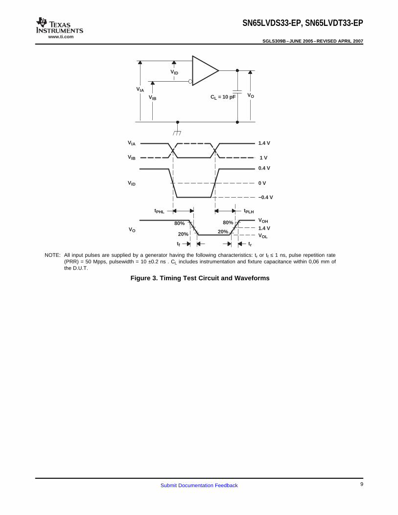
NOTE: All input pulses are supplied by a generator having the following characteristics: tr or tf ≤ 1 ns, pulse repetition rate(PRR) = 50 Mpps, pulsewidth = 10 ±0.2 ns . CL includes instrumentation and fixture capacitance within 0,06 mm ofthe D.U.T.
Figure 3. Timing Test Circuit and Waveforms
9Submit Documentation Feedback

www.ti.com
B
A
G
G
VO ±
500 Ω
VTEST
10 pF
1.2 V
tPZL
tPLZ
tPZL
tPLZ
tPZH
tPHZ
tPZH
tPHZ
2.5 V
1 V2 V1.4 V0.8 V
2 V1.4 V0.8 V
2.5 V1.4 VVOL +0.5 VVOL
01.4 V
2 V1.4 V0.8 V
2 V1.4 V0.8 V
VOHVOH −0.5 V1.4 V0
VTEST
A
G
G
Y
VTEST
A
G
Y
Inputs
G
NOTE: All input pulses are supplied by a generator having the following characteristics: tr or tf ≤ 1 ns, pulserepetition rate (PRR) = 0.5 Mpps, pulsewidth = 500 ±10 ns . CL includes instrumentation and fixturecapacitance within 0,06 mm of the D.U.T.
SN65LVDS33-EP, SN65LVDT33-EP
SGLS309B–JUNE 2005–REVISED APRIL 2007
Figure 4. Enable/Disable Time Test Circuit and Waveforms
10 Submit Documentation Feedback

www.ti.com
VIA
VIB
VO
−100 mV @ 250 KHz
a) No Failsafe
−32 mV @ 250 KHz
Failsafe Asserted
VIA
VIB
VO
b) Failsafe Asserted
td1 td2
1.4 V
1 V
0.4 V
0 V
−0.4 V
VOH
1.4 VVOL
−0.2 V
>1.5 µs
SN65LVDS33-EP, SN65LVDT33-EP
SGLS309B–JUNE 2005–REVISED APRIL 2007
Table 1. Receiver Minimum and Maximum VIT3 Input Threshold Test Voltages
APPLIED VOLTAGES (1) RESULTANT INPUTS
VIA (mV) VIB (mV) VID (mV) VIC (mV) Output
–4000 –3900 –100 –3950 L
–4000 –3968 –32 –3984 H
4900 5000 –100 4950 L
4968 5000 –32 4984 H
(1) These voltages are applied for a minimum of 1.5 µs.
Figure 5. VIT3 Failsafe Threshold Test
Figure 6. Waveforms for Failsafe Activate and Deactivate
11Submit Documentation Feedback

www.ti.com
TYPICAL CHARACTERISTICS
0
IOL − Low-Level Output Current − mA
4
3
020 30
2
10
VCC = 3.3 VTA = 25°C
1
VO
L−
Low
-Lev
el O
utpu
t Vol
tage
− V
5
40
IOH − High-Level Output Current − mA
VO
H−
Hig
h-Le
vel O
utpu
t Vol
tage
− V
4
3
0
2
1
−30 −20−40 0−10
VCC = 3.3 VTA = 25°C
4.5
4
3.5
3−50 0 50
5
100TA − Free-Air T emperature − °C
VCC = 3 V
VCC = 3.6 V
VCC = 3.3 V
− Lo
w-T
o-H
igh
Pro
paga
tion
Del
ay T
ime
− ns
t PLH
4.5
4
3.5
3−50 0 50
5
100TA − Free-Air T emperature − °C
VCC = 3.3 V
VCC = 3 V
VCC = 3.6 V
− H
igh-
To-
Low
Pro
paga
tion
Del
ay T
ime
− ns
t PH
L
SN65LVDS33-EP, SN65LVDT33-EP
SGLS309B–JUNE 2005–REVISED APRIL 2007
LOW-LEVEL OUTPUT VOLTAGE HIGH-LEVEL OUTPUT VOLTAGEvs vs
LOW-LEVEL OUTPUT CURRENT HIGH-LEVEL OUTPUT CURRENT
Figure 7. Figure 8.
LOW-TO-HIGH PROPAGATION DELAY TIME HIGH-TO-LOW PROPAGATION DELAY TIMEvs vs
FREE-AIR TEMPERATURE FREE-AIR TEMPERATURE
Figure 9. Figure 10.
12 Submit Documentation Feedback

www.ti.com
80
60
20
00 100
100
120
150 200
40− S
uppl
y C
urre
nt −
mA
I CC
f − Switching Frequency − MHz
VCC = 3 V
VCC = 3.6 V
VCC = 3.3 V
140
SN65LVDS33-EP, SN65LVDT33-EP
SGLS309B–JUNE 2005–REVISED APRIL 2007
TYPICAL CHARACTERISTICS (continued)
SUPPLY CURRENTvs
FREQUENCY
Figure 11.
13Submit Documentation Feedback

www.ti.com
APPLICATION INFORMATION
1B
1A
1Y
G
2Y
2A
2B
GND
VCC
4B
4A
4Y
G
3Y
3A
3B
1
2
3
4
5
6
7
8
16
15
14
13
12
11
10
9
100 Ω
100 Ω
100 Ω(see Note B)
100 Ω
VCC
See Note C
≈3.6 V
0.1 µF(see Note A)
1N645(2 places)
0.01 µF
5 V
RELATED INFORMATION
SN65LVDS33-EP, SN65LVDT33-EP
SGLS309B–JUNE 2005–REVISED APRIL 2007
A. Place a 0.1-µF Z5U ceramic, mica or polystyrene dielectric, 0805 size, chip capacitor between VCC and the groundplane. The capacitor should be located as close as possible to the device terminals.
B. The termination resistance value should match the nominal characteristic impedance of the transmission media with±10%.
C. Unused enable inputs should be tied to VCC or GND as appropriate.
Figure 12. Operation With 5-V Supply
IBIS modeling is available for this device. Contact the local Texas Instruments sales office or the TexasInstruments Web site at www.ti.com for more information.
For more application guidelines, see the following documents:• Low-Voltage Differential Signalling Design Notes (SLLA014)• Interface Circuits for TIA/EIA-644 (LVDS) (SLLA038)• Reducing EMI With LVDS (SLLA030)• Slew Rate Control of LVDS Circuits (SLLA034)• Using an LVDS Receiver With RS-422 Data (SLLA031)• Evaluating the LVDS EVM (SLLA033)
14 Submit Documentation Feedback

www.ti.com
ACTIVE FAILSAFE FEATURE
_+
Main Receiver
_+
_+
A > B + 80 mV
B > A + 80 mV
FailsafeTimer
Failsafe
OutputBuffer
Reset
Window Comparator
A
B R
SN65LVDS33-EP, SN65LVDT33-EP
SGLS309B–JUNE 2005–REVISED APRIL 2007
APPLICATION INFORMATION (continued)
A differential line receiver commonly has a failsafe circuit to prevent it from switching on input noise. CurrentLVDS failsafe solutions require either external components with subsequent reductions in signal quality orintegrated solutions with limited application. This family of receivers has a new integrated failsafe that solves thelimitations seen in present solutions. A detailed theory of operation is presented in application note, The ActiveFailsafe Feature of the SN65LVDS32B (SLLA082A).
Figure 13 shows one receiver channel with active failsafe. It consists of a main receiver that can respond to ahigh-speed input differential signal. Also connected to the input pair are two failsafe receivers that form a windowcomparator. The window comparator has a much slower response than the main receiver and it detects whenthe input differential falls below 80 mV. A 600-ns failsafe timer filters the window comparator outputs. Whenfailsafe is asserted, the failsafe logic drives the main receiver output to logic high.
Figure 13. Receiver With Active Failsafe
15Submit Documentation Feedback

www.ti.com
ECL/PECL-to-LVTTL CONVERSION WITH TI's LVDS RECEIVER
R3 R3
VCC
ICC
5 Metersof CAT-5
R1 R1
VEE R2
VCC
ICC
R3 = 240 Ω
R1 = 50 ΩR2 = 50 Ω
VB
VBLVDSLV/PECL
SN65LVDS33-EP, SN65LVDT33-EP
SGLS309B–JUNE 2005–REVISED APRIL 2007
APPLICATION INFORMATION (continued)
The various versions of emitter-coupled logic (i.e., ECL, PECL and LVPECL) are often the physical layer ofchoice for system designers. Designers know of the established technology and that it is capable of high-speeddata transmission. In the past, system requirements often forced the selection of ECL. Now technologies likeLVDS provide designers with another alternative. While the total exchange of ECL for LVDS may not be adesign option, designers have been able to take advantage of LVDS by implementing a small resistor dividernetwork at the input of the LVDS receiver. Texas Instruments has taken the next step by introducing a widecommon-mode LVDS receiver (no divider network required) which can be connected directly to an ECL driverwith only the termination bias voltage required for ECL termination (VCC – 2 V).
Figure 14 and Figure 15 show the use of an LV/PECL driver driving five meters of CAT-5 cable and beingreceived by Texas Instruments wide common-mode receiver and the resulting eye-pattern. The values for R3are required in order to provide a resistor path to ground for the LV/PECL driver. With no resistor divider, R1simply needs to match the characteristic load impedance of 50 Ω. The R2 resistor is a small value and isintended to minimize any possible common-mode current reflections.
Figure 14. LVPECL or PECL to Remote Wide Common-Mode LVDS Receiver
Figure 15. LV/PECL to Remote SN65LVDS33 at 500 Mbps Receiver Output (CH1)
16 Submit Documentation Feedback

www.ti.com
TEST CONDITIONS
EQUIPMENT
Tektronix PS25216ProgrammablePower Supply
Bench T est Board
Tektronix HFS 9003Stimulus System
Tektronix TDS 784D 4-ChannelDigital Phosphor Oscilloscope
− DPO
Trigger
100 Mbit/s 200 Mbit/s
SN65LVDS33-EP, SN65LVDT33-EP
SGLS309B–JUNE 2005–REVISED APRIL 2007
APPLICATION INFORMATION (continued)
• VCC = 3.3 V• TA = 25°C (ambient temperature)• All four channels switching simultaneously with NRZ data. The scope is pulse-triggered simultaneously with
NRZ data.
• Tektronix PS25216 programmable power supply• Tektronix HFS 9003 stimulus system• Tektronix TDS 784D 4-channel digital phosphor oscilloscope – DPO
Figure 16. Equipment Setup
Figure 17. Typical Eye Pattern SN65LVDS33
17Submit Documentation Feedback

PACKAGE OPTION ADDENDUM
www.ti.com 10-Dec-2020
Addendum-Page 1
PACKAGING INFORMATION
Orderable Device Status(1)
Package Type PackageDrawing
Pins PackageQty
Eco Plan(2)
Lead finish/Ball material
(6)
MSL Peak Temp(3)
Op Temp (°C) Device Marking(4/5)
Samples
SN65LVDS33MDREP ACTIVE SOIC D 16 2500 RoHS & Green NIPDAU Level-1-260C-UNLIM -55 to 125 LVDS33M
V62/05614-01XE ACTIVE SOIC D 16 2500 RoHS & Green NIPDAU Level-1-260C-UNLIM -55 to 125 LVDS33M
(1) The marketing status values are defined as follows:ACTIVE: Product device recommended for new designs.LIFEBUY: TI has announced that the device will be discontinued, and a lifetime-buy period is in effect.NRND: Not recommended for new designs. Device is in production to support existing customers, but TI does not recommend using this part in a new design.PREVIEW: Device has been announced but is not in production. Samples may or may not be available.OBSOLETE: TI has discontinued the production of the device.
(2) RoHS: TI defines "RoHS" to mean semiconductor products that are compliant with the current EU RoHS requirements for all 10 RoHS substances, including the requirement that RoHS substancedo not exceed 0.1% by weight in homogeneous materials. Where designed to be soldered at high temperatures, "RoHS" products are suitable for use in specified lead-free processes. TI mayreference these types of products as "Pb-Free".RoHS Exempt: TI defines "RoHS Exempt" to mean products that contain lead but are compliant with EU RoHS pursuant to a specific EU RoHS exemption.Green: TI defines "Green" to mean the content of Chlorine (Cl) and Bromine (Br) based flame retardants meet JS709B low halogen requirements of <=1000ppm threshold. Antimony trioxide basedflame retardants must also meet the <=1000ppm threshold requirement.
(3) MSL, Peak Temp. - The Moisture Sensitivity Level rating according to the JEDEC industry standard classifications, and peak solder temperature.
(4) There may be additional marking, which relates to the logo, the lot trace code information, or the environmental category on the device.
(5) Multiple Device Markings will be inside parentheses. Only one Device Marking contained in parentheses and separated by a "~" will appear on a device. If a line is indented then it is a continuationof the previous line and the two combined represent the entire Device Marking for that device.
(6) Lead finish/Ball material - Orderable Devices may have multiple material finish options. Finish options are separated by a vertical ruled line. Lead finish/Ball material values may wrap to twolines if the finish value exceeds the maximum column width.
Important Information and Disclaimer:The information provided on this page represents TI's knowledge and belief as of the date that it is provided. TI bases its knowledge and belief on informationprovided by third parties, and makes no representation or warranty as to the accuracy of such information. Efforts are underway to better integrate information from third parties. TI has taken andcontinues to take reasonable steps to provide representative and accurate information but may not have conducted destructive testing or chemical analysis on incoming materials and chemicals.TI and TI suppliers consider certain information to be proprietary, and thus CAS numbers and other limited information may not be available for release.
In no event shall TI's liability arising out of such information exceed the total purchase price of the TI part(s) at issue in this document sold by TI to Customer on an annual basis.

PACKAGE OPTION ADDENDUM
www.ti.com 10-Dec-2020
Addendum-Page 2
OTHER QUALIFIED VERSIONS OF SN65LVDS33-EP :
• Catalog: SN65LVDS33
NOTE: Qualified Version Definitions:
• Catalog - TI's standard catalog product

TAPE AND REEL INFORMATION
*All dimensions are nominal
Device PackageType
PackageDrawing
Pins SPQ ReelDiameter
(mm)
ReelWidth
W1 (mm)
A0(mm)
B0(mm)
K0(mm)
P1(mm)
W(mm)
Pin1Quadrant
SN65LVDS33MDREP SOIC D 16 2500 330.0 16.4 6.5 10.3 2.1 8.0 16.0 Q1
PACKAGE MATERIALS INFORMATION
www.ti.com 12-Feb-2019
Pack Materials-Page 1

*All dimensions are nominal
Device Package Type Package Drawing Pins SPQ Length (mm) Width (mm) Height (mm)
SN65LVDS33MDREP SOIC D 16 2500 350.0 350.0 43.0
PACKAGE MATERIALS INFORMATION
www.ti.com 12-Feb-2019
Pack Materials-Page 2


IMPORTANT NOTICE AND DISCLAIMER
TI PROVIDES TECHNICAL AND RELIABILITY DATA (INCLUDING DATASHEETS), DESIGN RESOURCES (INCLUDING REFERENCE DESIGNS), APPLICATION OR OTHER DESIGN ADVICE, WEB TOOLS, SAFETY INFORMATION, AND OTHER RESOURCES “AS IS” AND WITH ALL FAULTS, AND DISCLAIMS ALL WARRANTIES, EXPRESS AND IMPLIED, INCLUDING WITHOUT LIMITATION ANY IMPLIED WARRANTIES OF MERCHANTABILITY, FITNESS FOR A PARTICULAR PURPOSE OR NON-INFRINGEMENT OF THIRD PARTY INTELLECTUAL PROPERTY RIGHTS.These resources are intended for skilled developers designing with TI products. You are solely responsible for (1) selecting the appropriate TI products for your application, (2) designing, validating and testing your application, and (3) ensuring your application meets applicable standards, and any other safety, security, or other requirements. These resources are subject to change without notice. TI grants you permission to use these resources only for development of an application that uses the TI products described in the resource. Other reproduction and display of these resources is prohibited. No license is granted to any other TI intellectual property right or to any third party intellectual property right. TI disclaims responsibility for, and you will fully indemnify TI and its representatives against, any claims, damages, costs, losses, and liabilities arising out of your use of these resources.TI’s products are provided subject to TI’s Terms of Sale (www.ti.com/legal/termsofsale.html) or other applicable terms available either on ti.com or provided in conjunction with such TI products. TI’s provision of these resources does not expand or otherwise alter TI’s applicable warranties or warranty disclaimers for TI products.
Mailing Address: Texas Instruments, Post Office Box 655303, Dallas, Texas 75265Copyright © 2020, Texas Instruments Incorporated