sn65hvd25x turbo can bus transceivers for highly … · sn65hvd255, sn65hvd256, sn65hvd257 sllsea2d...
TRANSCRIPT
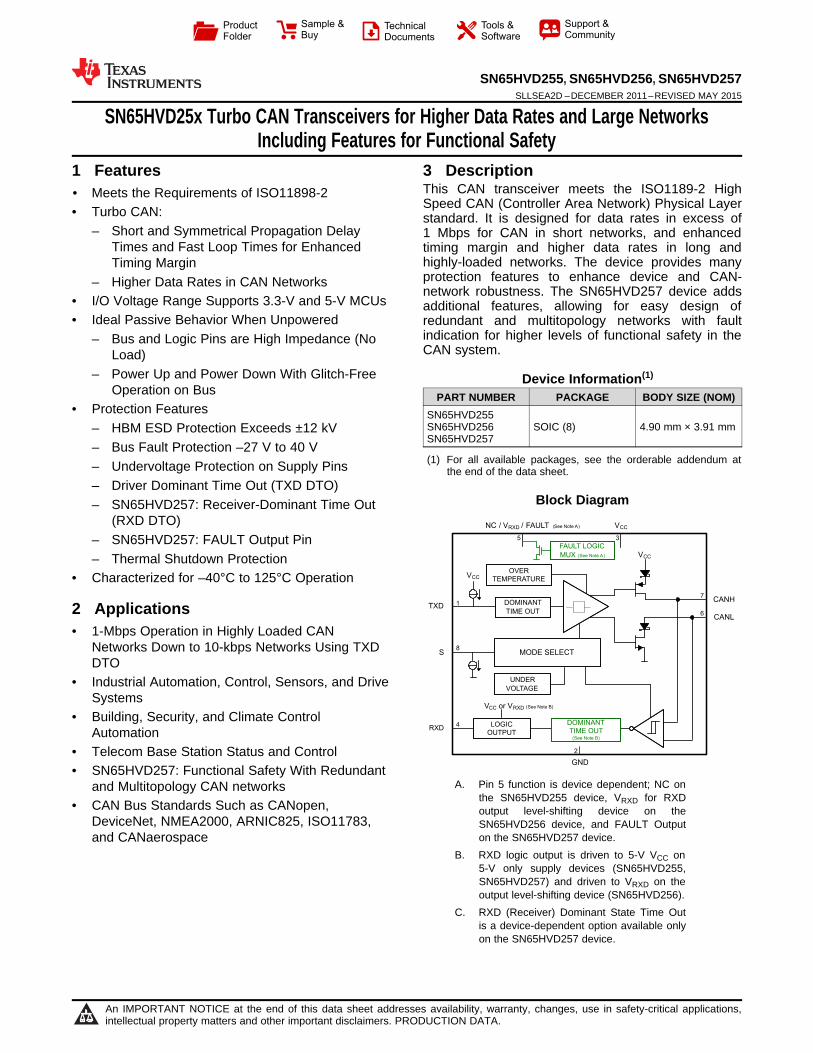
VCC
CANH7
6CANL
RXD
1TXD
S8
DOMINANT
TIME OUT
OVERTEMPERATURE
LOGICOUTPUT
MODE SELECT
4
NC / VRXD / FAULT (See Note A) VCC
5 3
GND
2
UNDER
VOLTAGE
DOMINANTTIME OUT
(See Note B)
VCC
VCC or VRXD (See Note B)
FAULT LOGIC
MUX (See Note A)
Product
Folder
Sample &Buy
Technical
Documents
Tools &
Software
Support &Community
SN65HVD255, SN65HVD256, SN65HVD257SLLSEA2D –DECEMBER 2011–REVISED MAY 2015
SN65HVD25x Turbo CAN Transceivers for Higher Data Rates and Large NetworksIncluding Features for Functional Safety
1 Features 3 DescriptionThis CAN transceiver meets the ISO1189-2 High
1• Meets the Requirements of ISO11898-2Speed CAN (Controller Area Network) Physical Layer• Turbo CAN: standard. It is designed for data rates in excess of
– Short and Symmetrical Propagation Delay 1 Mbps for CAN in short networks, and enhancedTimes and Fast Loop Times for Enhanced timing margin and higher data rates in long and
highly-loaded networks. The device provides manyTiming Marginprotection features to enhance device and CAN-– Higher Data Rates in CAN Networksnetwork robustness. The SN65HVD257 device adds
• I/O Voltage Range Supports 3.3-V and 5-V MCUs additional features, allowing for easy design of• Ideal Passive Behavior When Unpowered redundant and multitopology networks with fault
indication for higher levels of functional safety in the– Bus and Logic Pins are High Impedance (NoCAN system.Load)
– Power Up and Power Down With Glitch-Free Device Information(1)
Operation on Bus PART NUMBER PACKAGE BODY SIZE (NOM)• Protection Features SN65HVD255
SN65HVD256 SOIC (8) 4.90 mm × 3.91 mm– HBM ESD Protection Exceeds ±12 kVSN65HVD257
– Bus Fault Protection –27 V to 40 V(1) For all available packages, see the orderable addendum at– Undervoltage Protection on Supply Pins the end of the data sheet.
– Driver Dominant Time Out (TXD DTO)Block Diagram– SN65HVD257: Receiver-Dominant Time Out
(RXD DTO)– SN65HVD257: FAULT Output Pin– Thermal Shutdown Protection
• Characterized for –40°C to 125°C Operation
2 Applications• 1-Mbps Operation in Highly Loaded CAN
Networks Down to 10-kbps Networks Using TXDDTO
• Industrial Automation, Control, Sensors, and DriveSystems
• Building, Security, and Climate ControlAutomation
• Telecom Base Station Status and Control• SN65HVD257: Functional Safety With Redundant
A. Pin 5 function is device dependent; NC onand Multitopology CAN networksthe SN65HVD255 device, VRXD for RXD• CAN Bus Standards Such as CANopen, output level-shifting device on the
DeviceNet, NMEA2000, ARNIC825, ISO11783, SN65HVD256 device, and FAULT Outputon the SN65HVD257 device.and CANaerospace
B. RXD logic output is driven to 5-V VCC on5-V only supply devices (SN65HVD255,SN65HVD257) and driven to VRXD on theoutput level-shifting device (SN65HVD256).
C. RXD (Receiver) Dominant State Time Outis a device-dependent option available onlyon the SN65HVD257 device.
1
An IMPORTANT NOTICE at the end of this data sheet addresses availability, warranty, changes, use in safety-critical applications,intellectual property matters and other important disclaimers. PRODUCTION DATA.
SN65HVD255, SN65HVD256, SN65HVD257SLLSEA2D –DECEMBER 2011–REVISED MAY 2015 www.ti.com
Table of Contents9.1 Overview ................................................................. 141 Features .................................................................. 19.2 Functional Block Diagram ....................................... 142 Applications ........................................................... 19.3 Feature Description................................................. 143 Description ............................................................. 19.4 Device Functional Modes........................................ 194 Revision History..................................................... 2
10 Application and Implementation........................ 225 Device Options....................................................... 410.1 Application Information.......................................... 226 Pin Configuration and Functions ......................... 410.2 Typical Applications .............................................. 237 Specifications......................................................... 5 11 Power Supply Recommendations ..................... 277.1 Absolute Maximum Ratings ...................................... 5
12 Layout................................................................... 277.2 ESD Ratings.............................................................. 512.1 Layout Guidelines ................................................. 277.3 Recommended Operating Conditions....................... 612.2 Layout Example .................................................... 287.4 Thermal Information .................................................. 6
13 Device and Documentation Support ................. 287.5 Electrical Characteristics........................................... 713.1 Related Links ........................................................ 287.6 Power Dissipation ..................................................... 913.2 Trademarks ........................................................... 287.7 Switching Characteristics .......................................... 913.3 Electrostatic Discharge Caution............................ 287.8 Typical Characteristics ............................................ 1013.4 Glossary ................................................................ 288 Parameter Measurement Information ................ 11
14 Mechanical, Packaging, and Orderable9 Detailed Description ............................................ 14 Information ........................................................... 28
4 Revision History
Changes from Revision C (September 2013) to Revision D Page
• Added Pin Configuration and Functions section, ESD Ratings table, Switching Characteristics table, TypicalCharacteristics section, Feature Description section, Device Functional Modes, Application and Implementationsection, Power Supply Recommendations section, Layout section, Device and Documentation Support section, andMechanical, Packaging, and Orderable Information section ................................................................................................. 1
Changes from Revision B (June 2012) to Revision C Page
• Added Table 1, Receiver Differential Input Voltage Threshold Test .................................................................................... 12• Added Figure 13, Example Timing Diagram for TXD DTO and FAULT Pin ........................................................................ 17• Added Bus Loading, Length, and Number of Nodes subsection ......................................................................................... 22
Changes from Revision A (June 2012) to Revision B Page
• Added SN65HVD257 status to production in Ordering Information table .............................................................................. 4
Changes from Original (December 2011) to Revision A Page
• Updated the Features list ....................................................................................................................................................... 1• Updated the Applications list .................................................................................................................................................. 1• Added text to the Description section..................................................................................................................................... 1• Changed Block Diagram - Functional Block Diagram to include HVD257 and Note changes............................................... 1• Changed the DEVICE OPTIONS table................................................................................................................................... 4• Added SN65HVD257 to the D PACKAGE OPTIONS images................................................................................................ 4• Added SN65HVD257 FAULT pin to the PIN FUNCTIONS table ........................................................................................... 4• Added SN65HVD257 to the Ordering Information table......................................................................................................... 4• Added SN65HVD257 FAULT pin information to the Abs Max table ...................................................................................... 5• Added FAULT pin information to the ROC table .................................................................................................................... 6
2 Submit Documentation Feedback Copyright © 2011–2015, Texas Instruments Incorporated
Product Folder Links: SN65HVD255 SN65HVD256 SN65HVD257

SN65HVD255, SN65HVD256, SN65HVD257www.ti.com SLLSEA2D –DECEMBER 2011–REVISED MAY 2015
• changed RID - Differential input resistance value from 3 kΩ to 30 kΩ.................................................................................... 8• Added tRXD_DTO - SN65HVD257 information ......................................................................................................................... 10• Added Figure 4, RXD Dominant Timeout Test Circuit and Measurement ........................................................................... 11• Added Figure 5, FAULT Test and Measurement ................................................................................................................. 11• Added RXD Dominant Timeout (SN65HVD257) section...................................................................................................... 15• Added FAULT pin information .............................................................................................................................................. 16• Added footnote for SN65HVD257 function to Table 5 ......................................................................................................... 19• Added 5-V VCC with FAULT Open-Drain Output Device (SN65HVD257) section................................................................ 21• Added Example: Functional Safety Using the SN65HVD257 in a Redundant Physical Layer CAN Network Topology
section .................................................................................................................................................................................. 24
Copyright © 2011–2015, Texas Instruments Incorporated Submit Documentation Feedback 3
Product Folder Links: SN65HVD255 SN65HVD256 SN65HVD257

S
CANL
FAULT
SN65HVD257
5-V Supply and Fault
Output
TXD
RXD
GND
VCC
CANH
1
2
3
4
8
7
6
5
SN65HVD256
S
CANH
CANL
5-V Supply with RXD
Level-Shifting
TXD
RXD
GND
VCC
VRXD
1
2
3
4
8
7
6
5
SN65HVD255
5-V Supply
TXD
RXD
GND
VCC
S
CANH
CANL
NC
1
2
3
4
8
7
6
5
SN65HVD255, SN65HVD256, SN65HVD257SLLSEA2D –DECEMBER 2011–REVISED MAY 2015 www.ti.com
5 Device Options
I/O TXD RXD FAULTSUPPLYPART NUMBER COMMENTDTO DTO Outputfor RXD'251 and '1050 functional upgrade with Turbo CAN fast loop times andSN65HVD255 No Yes No No TXD DTO protection allowing data rates down to 10 kbps'251 and '1050 functional upgrade with Turbo CAN fast loop times and
SN65HVD256 Yes Yes No No TXD DTO protection allowing data rates down to 10 kbps. RXD outputlevel shifting through RXD supply input.'251 and '1050 functional upgrade with Turbo CAN fast loop times, TXD
SN65HVD257 No Yes Yes Yes and RXD DTO protection allowing data rates down to 10 kbps and faultoutput pin
6 Pin Configuration and Functions
D Package8-Pin SOIC(Top View)
Pin FunctionsPIN
TYPE DESCRIPTIONNAME NO.
TXD 1 I CAN transmit data input (LOW for dominant and HIGH for recessive bus states)GND 2 GND Ground connectionVCC 3 Supply Transceiver 5-V supply voltageRXD 4 O CAN receive data output (LOW for dominant and HIGH for recessive bus states)NC NC SN65HVD255: No ConnectVRXD 5 Supply SN65HVD256: RXD output supply voltageFAULT O SN65HVD257: Open drain FAULT output pinCANL 6 I/O Low level CAN bus lineCANH 7 I/O High level CAN bus lineS 8 I Mode select: S (silent mode) select pin (active high)
4 Submit Documentation Feedback Copyright © 2011–2015, Texas Instruments Incorporated
Product Folder Links: SN65HVD255 SN65HVD256 SN65HVD257
SN65HVD255, SN65HVD256, SN65HVD257www.ti.com SLLSEA2D –DECEMBER 2011–REVISED MAY 2015
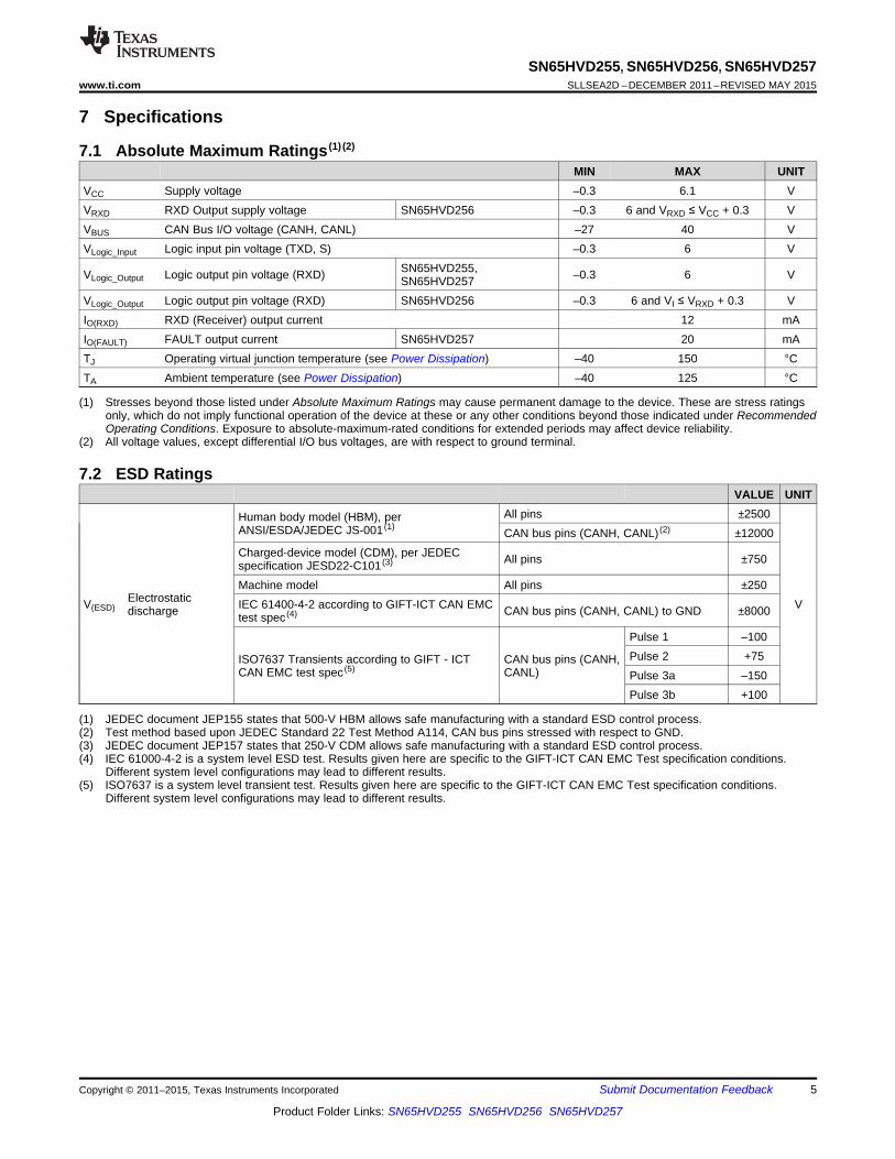
7 Specifications
7.1 Absolute Maximum Ratings (1) (2)
MIN MAX UNITVCC Supply voltage –0.3 6.1 VVRXD RXD Output supply voltage SN65HVD256 –0.3 6 and VRXD ≤ VCC + 0.3 VVBUS CAN Bus I/O voltage (CANH, CANL) –27 40 VVLogic_Input Logic input pin voltage (TXD, S) –0.3 6 V
SN65HVD255,VLogic_Output Logic output pin voltage (RXD) –0.3 6 VSN65HVD257VLogic_Output Logic output pin voltage (RXD) SN65HVD256 –0.3 6 and VI ≤ VRXD + 0.3 VIO(RXD) RXD (Receiver) output current 12 mAIO(FAULT) FAULT output current SN65HVD257 20 mATJ Operating virtual junction temperature (see Power Dissipation) –40 150 °CTA Ambient temperature (see Power Dissipation) –40 125 °C
(1) Stresses beyond those listed under Absolute Maximum Ratings may cause permanent damage to the device. These are stress ratingsonly, which do not imply functional operation of the device at these or any other conditions beyond those indicated under RecommendedOperating Conditions. Exposure to absolute-maximum-rated conditions for extended periods may affect device reliability.
(2) All voltage values, except differential I/O bus voltages, are with respect to ground terminal.
7.2 ESD RatingsVALUE UNIT
All pins ±2500Human body model (HBM), perANSI/ESDA/JEDEC JS-001 (1) CAN bus pins (CANH, CANL) (2) ±12000Charged-device model (CDM), per JEDEC All pins ±750specification JESD22-C101 (3)
Machine model All pins ±250ElectrostaticV(ESD) IEC 61400-4-2 according to GIFT-ICT CAN EMC Vdischarge CAN bus pins (CANH, CANL) to GND ±8000test spec (4)
Pulse 1 –100Pulse 2 +75ISO7637 Transients according to GIFT - ICT CAN bus pins (CANH,
CAN EMC test spec (5) CANL) Pulse 3a –150Pulse 3b +100
(1) JEDEC document JEP155 states that 500-V HBM allows safe manufacturing with a standard ESD control process.(2) Test method based upon JEDEC Standard 22 Test Method A114, CAN bus pins stressed with respect to GND.(3) JEDEC document JEP157 states that 250-V CDM allows safe manufacturing with a standard ESD control process.(4) IEC 61000-4-2 is a system level ESD test. Results given here are specific to the GIFT-ICT CAN EMC Test specification conditions.
Different system level configurations may lead to different results.(5) ISO7637 is a system level transient test. Results given here are specific to the GIFT-ICT CAN EMC Test specification conditions.
Different system level configurations may lead to different results.
Copyright © 2011–2015, Texas Instruments Incorporated Submit Documentation Feedback 5
Product Folder Links: SN65HVD255 SN65HVD256 SN65HVD257
SN65HVD255, SN65HVD256, SN65HVD257SLLSEA2D –DECEMBER 2011–REVISED MAY 2015 www.ti.com
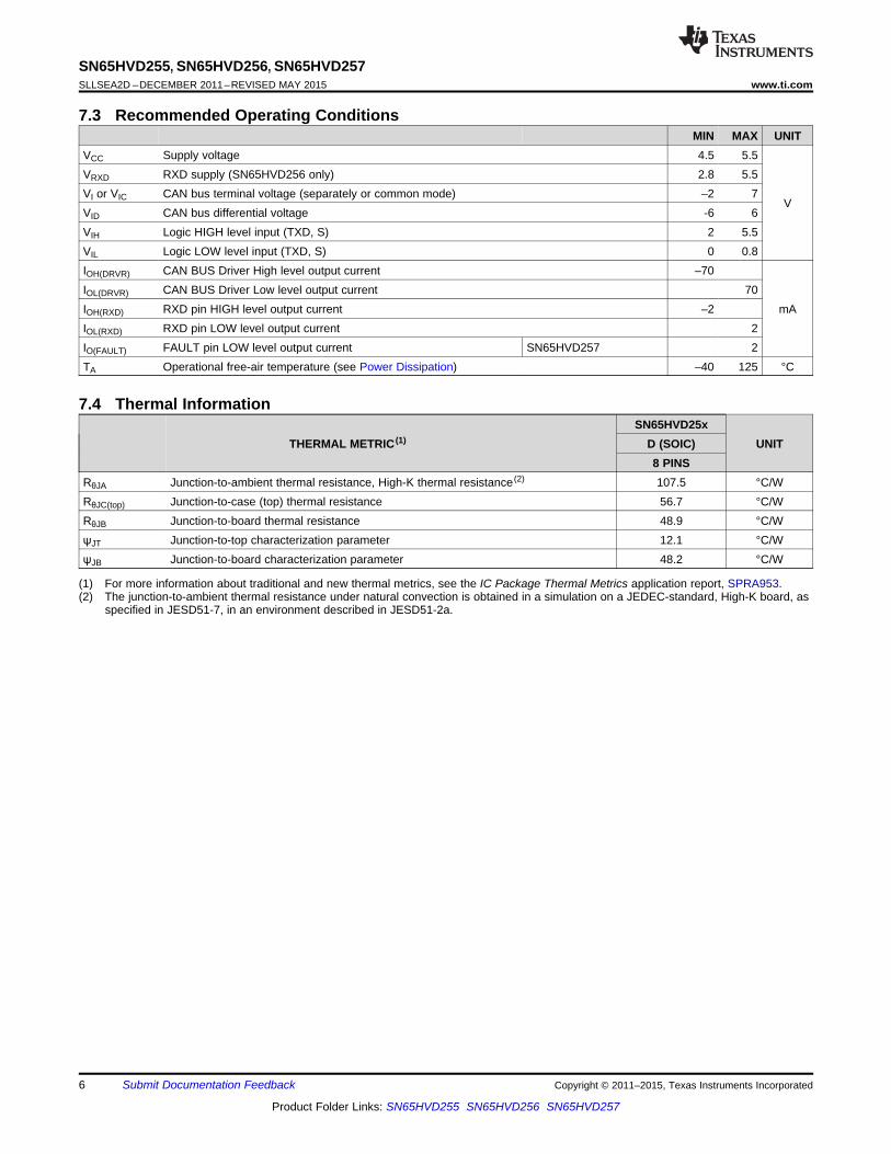
7.3 Recommended Operating ConditionsMIN MAX UNIT
VCC Supply voltage 4.5 5.5VRXD RXD supply (SN65HVD256 only) 2.8 5.5VI or VIC CAN bus terminal voltage (separately or common mode) –2 7
VVID CAN bus differential voltage -6 6VIH Logic HIGH level input (TXD, S) 2 5.5VIL Logic LOW level input (TXD, S) 0 0.8IOH(DRVR) CAN BUS Driver High level output current –70IOL(DRVR) CAN BUS Driver Low level output current 70IOH(RXD) RXD pin HIGH level output current –2 mAIOL(RXD) RXD pin LOW level output current 2IO(FAULT) FAULT pin LOW level output current SN65HVD257 2TA Operational free-air temperature (see Power Dissipation) –40 125 °C
7.4 Thermal InformationSN65HVD25x
THERMAL METRIC (1) D (SOIC) UNIT8 PINS
RθJA Junction-to-ambient thermal resistance, High-K thermal resistance (2) 107.5 °C/WRθJC(top) Junction-to-case (top) thermal resistance 56.7 °C/WRθJB Junction-to-board thermal resistance 48.9 °C/WψJT Junction-to-top characterization parameter 12.1 °C/WψJB Junction-to-board characterization parameter 48.2 °C/W
(1) For more information about traditional and new thermal metrics, see the IC Package Thermal Metrics application report, SPRA953.(2) The junction-to-ambient thermal resistance under natural convection is obtained in a simulation on a JEDEC-standard, High-K board, as
specified in JESD51-7, in an environment described in JESD51-2a.
6 Submit Documentation Feedback Copyright © 2011–2015, Texas Instruments Incorporated
Product Folder Links: SN65HVD255 SN65HVD256 SN65HVD257
SN65HVD255, SN65HVD256, SN65HVD257www.ti.com SLLSEA2D –DECEMBER 2011–REVISED MAY 2015
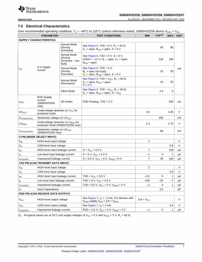
7.5 Electrical CharacteristicsOver recommended operating conditions, TA = –40°C to 125°C (unless otherwise noted). SN65HVD256 device VRXD = VCC.
PARAMETER TEST CONDITIONS MIN TYP (1) MAX UNITSUPPLY CHARACTERISTICS
Normal Mode See Figure 6, TXD = 0 V, RL = 50 Ω,(Driving 60 85CL = open, RCM = open, S = 0 VDominant)Normal Mode See Figure 6, TXD = 0 V, S = 0 V,(Driving CANH = –12 V, RL = open, CL = open, 130 180Dominant – bus
RCM = openfault)5-V Supply See Figure 6, TXD = 0 V,Normal ModeICC mAcurrent (Driving 10 20RL = open (no load),
Dominant) CL = open, RCM = open, S = 0 VSee Figure 6, TXD = VCC, RL = 50 Ω,Normal Mode 10 20CL = open, RCM = open,(Recessive) S = 0 VSee Figure 6, TXD = VCC, RL = 50 Ω,Silent Mode 2.5 5CL = open, RCM = open, S = VCC
RXD SupplycurrentIRXD All modes RXD Floating, TXD = 0 V 500 µA(SN65HVD256only)Undervoltage detection on VCC forUVVCC 3.5 4.45 Vprotected mode
VHYS(UVVCC) Hysteresis voltage on UVVCC 200 mVUndervoltage detection on VRXD forUVRXD 1.3 2.75 Vprotected mode (SN65HVD256 only)Hysteresis voltage on UVRXDVHYS(UVRXD) 80 mV(SN65HVD256 only)
S PIN (MODE SELECT INPUT)VIH HIGH-level input voltage 2 VVIL LOW-level input voltage 0.8 VIIH HIGH-level input leakage current S = VCC = 5.5 V 7 100 µAIIL Low-level input leakage current S = 0 V, VCC = 5.5 V –1 0 1 µAILKG(OFF) Unpowered leakage current S = 5.5 V, VCC = 0 V, VRXD = 0 V 7 35 100 µATXD PIN (CAN TRANSMIT DATA INPUT)VIH HIGH level input voltage 2 VVIL LOW level input voltage 0.8 VIIH HIGH level input leakage current TXD = VCC = 5.5 V –2.5 0 1 µAIIL Low level input leakage current TXD = 0 V, VCC = 5.5 V –100 –25 –7 µAILKG(OFF) Unpowered leakage current TXD = 5.5 V, VCC = 0 V, VRXD = 0 V –1 0 1 µACI Input Capacitance 3.5 pFRXD PIN (CAN RECEIVE DATA OUTPUT)
See Figure 7, IO = –2 mA. For devices withVOH HIGH level output voltage 0.8 × VCC VVRXD supply VOH = 0.8 × VRXD
VOL LOW level output voltage See Figure 7, IO = 2 mA 0.4 VILKG(OFF) Unpowered leakage current RXD = 5.5 V, VCC = 0 V, VRXD = 0 V –1 0 1 µA
(1) All typical values are at 25°C and supply voltages of VCC = 5 V and VRXD = 5 V, RL = 60 Ω.
Copyright © 2011–2015, Texas Instruments Incorporated Submit Documentation Feedback 7
Product Folder Links: SN65HVD255 SN65HVD256 SN65HVD257
SN65HVD255, SN65HVD256, SN65HVD257SLLSEA2D –DECEMBER 2011–REVISED MAY 2015 www.ti.com
Electrical Characteristics (continued)Over recommended operating conditions, TA = –40°C to 125°C (unless otherwise noted). SN65HVD256 device VRXD = VCC.
PARAMETER TEST CONDITIONS MIN TYP (1) MAX UNITDRIVER ELECTRICAL CHARACTERISTICS
CANH See Figure 15 and Figure 6, TXD = 0 V, 2.75 4.5Bus outputVO(D) voltage S = 0 V, RL = 60 Ω, CL = open, V
CANL 0.5 2.25(dominant) RCM = openSee Figure 15 and Figure 6, TXD = VCC,
VO(R) Bus output voltage (recessive) VRXD = VCC, S = VCC or 0 V (2), RL = open 2 0.5 × VCC 3 V(no load), RCM = openSee Figure 15 and Figure 6, TXD = 0 V,S = 0 V, 45 Ω ≤ RL ≤ 65 Ω, CL = open, 1.5 3RCM = 330 Ω, –2 V ≤ VCM ≤ 7 V, 4.75 V≤VCC ≤ 5.25 VDifferential output voltageVOD(D) V(dominant) See Figure 15 and Figure 6, TXD = 0 V, S= 0 V, 45 Ω ≤ RL ≤ 65 Ω, CL = open,
1.25 3.2RCM = 330 Ω, –2 V ≤ VCM ≤ 7 V,4.5 V ≤ VCC ≤ 5.5 VSee Figure 15 and Figure 6, TXD = VCC,S = 0 V, RL = 60 Ω, CL = open, –0.12 0.012RCM = openDifferential output voltageVOD(R) V(recessive) See Figure 15 and Figure 6, TXD = VCC,S = 0 V, RL = open (no load), CL = open, –0.100 0.050RCM = open, –40°C ≤ TA ≤ 85°C
Output symmetry (dominant or See Figure 15 and Figure 6, S at 0 V,recessive)VSYM –0.4 0.4 VRL = 60 Ω, CL = open, RCM = open(VCC – VO(CANH) – VO(CANL))See Figure 15 and Figure 11, VCANH = 0 V, –160CANL = open, TXD = 0 VShort circuit steady-state outputIOS(SS)_DOM mAcurrent, Dominant See Figure 15 and Figure 11, 160VCANL = 32 V, CANH = open, TXD = 0 VSee Figure 15 and Figure 11,
Short circuit steady-state output –20 V ≤ VBUS ≤ 32 V, Where VBUS = CANHIOS(SS)_REC –8 8 mAcurrent, Recessive = CANL,TXD = VCC, Normal and Silent ModesSee Input capacitance to ground (CI) in the
CO Output capacitance following Receiver Electrical Characteristicssection of this table
RECEIVER ELECTRICAL CHARACTERISTICSPositive-going input thresholdVIT+ 900 mVvoltage, normal mode
See Figure 7, Table 5 and Table 1Negative-going input thresholdVIT– 500 mVvoltage, normal mode
VHYS Hysteresis voltage (VIT+ - VIT–) 125 mVVCANH = VCANL = 5 V,Power-off (unpowered) bus inputIIOFF(LKG) 5.5 µAleakage current VCC = 0 V, VRXD = 0 VTXD = VCC, VRXD = VCC,Input capacitance to ground (CANHCI 25 pFor CANL) VI = 0.4 sin (4E6 π t) + 2.5 VTXD = VCC, VRXD = VCC,CID Differential input capacitance 10 pFVI = 0.4 sin (4E6 π t)
RID Differential input resistance 30 80 kΩTXD = VCC = VRXD = 5 V, S = 0 V
RIN Input resistance (CANH or CANL) 15 40 kΩInput resistance matching:RIN(M) V(CANH) = V(CANL), –40°C ≤ TA ≤ 85°C –3% 3%[1 – RIN(CANH) / RIN(CANL)] × 100%
(2) For the bus output voltage (recessive) will be the same if the device is in normal mode with S pin LOW or if the device is in silent modewith the S pin HIGH.
8 Submit Documentation Feedback Copyright © 2011–2015, Texas Instruments Incorporated
Product Folder Links: SN65HVD255 SN65HVD256 SN65HVD257

SN65HVD255, SN65HVD256, SN65HVD257www.ti.com SLLSEA2D –DECEMBER 2011–REVISED MAY 2015
Electrical Characteristics (continued)Over recommended operating conditions, TA = –40°C to 125°C (unless otherwise noted). SN65HVD256 device VRXD = VCC.
PARAMETER TEST CONDITIONS MIN TYP (1) MAX UNITFAULT PIN (FAULT OUTPUT), SN65HVD257 ONLYICH Output current high level FAULT = VCC, see Figure 5 –10 10 µAICL Output current low level FAULT = 0.4 V, see Figure 5 5 12 mA
7.6 Power DissipationTHERMAL METRIC TEST CONDITIONS TYP UNIT
VCC = 5 V, VRXD = 5 V, TJ = 27°C, RL = 60 Ω, S at 0 V, Input to TXD at250 kHz, 25% duty cycle square wave, CL_RXD = 15 pF. Typical CAN 115operating conditions at 500 kbps with 25% transmission (dominant) rate.
PD Average power dissipation mWVCC = 5.5 V, VRXD = 5.5 V, TJ = 150°C, RL = 50 Ω, S at 0 V, Input to TXDat 500 kHz, 50% duty cycle square wave, CL_RXD = 15 pF. Typical high 268load CAN operating conditions at 1 Mbps with 50% transmission(dominant) rate and loaded network.
Thermal shutdown temperature 170 °CThermal shutdown hysteresis 5 °C
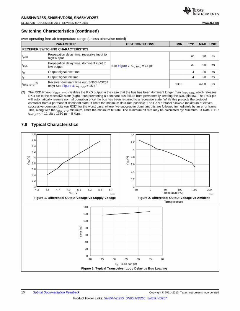
7.7 Switching Characteristicsover operating free-air temperature range (unless otherwise noted)
PARAMETER TEST CONDITIONS MIN TYP MAX UNITDEVICE SWITCHING CHARACTERISTICS
Total loop delay, driver input (TXD) totPROP(LOOP1) receiver output (RXD), recessive to 150
dominant See Figure 9, S = 0 V, RL = 60 Ω, nsCL = 100 pF, CL_RXD = 15 pFTotal loop delay, driver input (TXD) totPROP(LOOP2) receiver output (RXD), dominant to 150
recessiveMode change time, from Normal to SilentIMODE See Figure 8 20 µSor from Silent to Normal
DRIVER SWITCHING CHARACTERISTICSPropagation delay time, HIGH TXD totpHR 50 70Driver RecessivePropagation delay time, LOW TXD totpLD 40 70See Figure 6, S = 0 V, RL = 60 Ω,Driver Dominant nsCL = 100 pF, RCM = opentsk(p) Pulse skew (|tpHR – tpLD|) 10
tR Differential output signal rise time 10 30tF Differential output signal fall time 17 30
Differential output signal rise time,tR(10k) 35RL = 10 kΩ See Figure 6, S = 0 V, RL = 10 kΩ, nsCL = 10 pF, RCM = openDifferential output signal fall time,tF(10k) 100RL = 10 kΩtTXD_DTO Dominant timeout (1) See Figure 10, RL = 60 Ω, CL = open 1175 3700 µs
(1) The TXD dominant timeout (tTXD_DTO) disables the driver of the transceiver when the TXD has been dominant longer than tTXD_DTO,which releases the bus lines to recessive, thus preventing a local failure from locking the bus dominant. The driver may only transmitdominant again after TXD has been returned HIGH (recessive). While this protects the bus from local faults locking the bus dominant, itlimits the minimum data rate possible. The CAN protocol allows a maximum of eleven successive dominant bits (on TXD) for the worstcase, where five successive dominant bits are followed immediately by an error frame. This, along with the tTXD_DTO minimum, limits theminimum bit rate. The minimum bit rate may be calculated by: Minimum Bit Rate = 11 / tTXD_DTO = 11 bits / 1175 µs = 9.4 kbps.
Copyright © 2011–2015, Texas Instruments Incorporated Submit Documentation Feedback 9
Product Folder Links: SN65HVD255 SN65HVD256 SN65HVD257
0
20
40
60
80
100
120
140
40 45 50 55 60 65 70
Tim
e (n
s)
RL - Bus Load (:) C024
VCC (V)
VO
D (
V)
4.3 4.5 4.7 4.9 5.1 5.3 5.5 5.73
3.2
3.4
3.6
3.8
4
4.2
4.4
4.6
4.8
D001Temperature (qC)
VO
D (
V)
-50 0 50 100 150 2003
3.2
3.4
3.6
3.8
4
4.2
4.4
D002
SN65HVD255, SN65HVD256, SN65HVD257SLLSEA2D –DECEMBER 2011–REVISED MAY 2015 www.ti.com
Switching Characteristics (continued)over operating free-air temperature range (unless otherwise noted)
PARAMETER TEST CONDITIONS MIN TYP MAX UNITRECEIVER SWITCHING CHARACTERISTICS
Propagation delay time, recessive input totpRH 70 90 nshigh outputPropagation delay time, dominant input totpDL 70 90 nsSee Figure 7, CL_RXD = 15 pFlow output
tR Output signal rise time 4 20 nstF Output signal fall time 4 20 ns
Receiver dominant time out (SN65HVD257tRXD_DTO(2) 1380 4200 µsonly) See Figure 4, CL_RXD = 15 pF
(2) The RXD timeout (tRXD_DTO) disables the RXD output in the case that the bus has been dominant longer than tRXD_DTO, which releasesRXD pin to the recessive state (high), thus preventing a dominant bus failure from permanently keeping the RXD pin low. The RXD pinwill automatically resume normal operation once the bus has been returned to a recessive state. While this protects the protocolcontroller from a permanent dominant state, it limits the minimum data rate possible. The CAN protocol allows a maximum of elevensuccessive dominant bits (on RXD) for the worst case, where five successive dominant bits are followed immediately by an error frame.This, along with the tRXD_DTO minimum, limits the minimum bit rate. The minimum bit rate may be calculated by: Minimum Bit Rate = 11 /tRXD_DTO = 11 bits / 1380 µs = 8 kbps.
7.8 Typical Characteristics
Figure 1. Differential Output Voltage vs Supply Voltage Figure 2. Differential Output Voltage vs AmbientTemperature
Figure 3. Typical Transceiver Loop Delay vs Bus Loading
10 Submit Documentation Feedback Copyright © 2011–2015, Texas Instruments Incorporated
Product Folder Links: SN65HVD255 SN65HVD256 SN65HVD257
VODRL
CANH
CANL
TXD
RCM
RCM
VCMCL
TXD
0.9V
0.5 VVOD
tpLD tpHR
50% 50%
VO(CANH)
VO(CANL)
tR tF
0V
90%
10%
VCC
TXD
DTO
RXD
DTO
Thermal
Shutdown
FAULT
GND
+
-
IFAULT
UV
Lockout
VO
CANH
RXD
CANL
VID
50%
0.9V
0.5VVID
tRXD_DTO
0V
VID(D)
RXD
0V
VOH
CL_RXD
SN65HVD255, SN65HVD256, SN65HVD257www.ti.com SLLSEA2D –DECEMBER 2011–REVISED MAY 2015
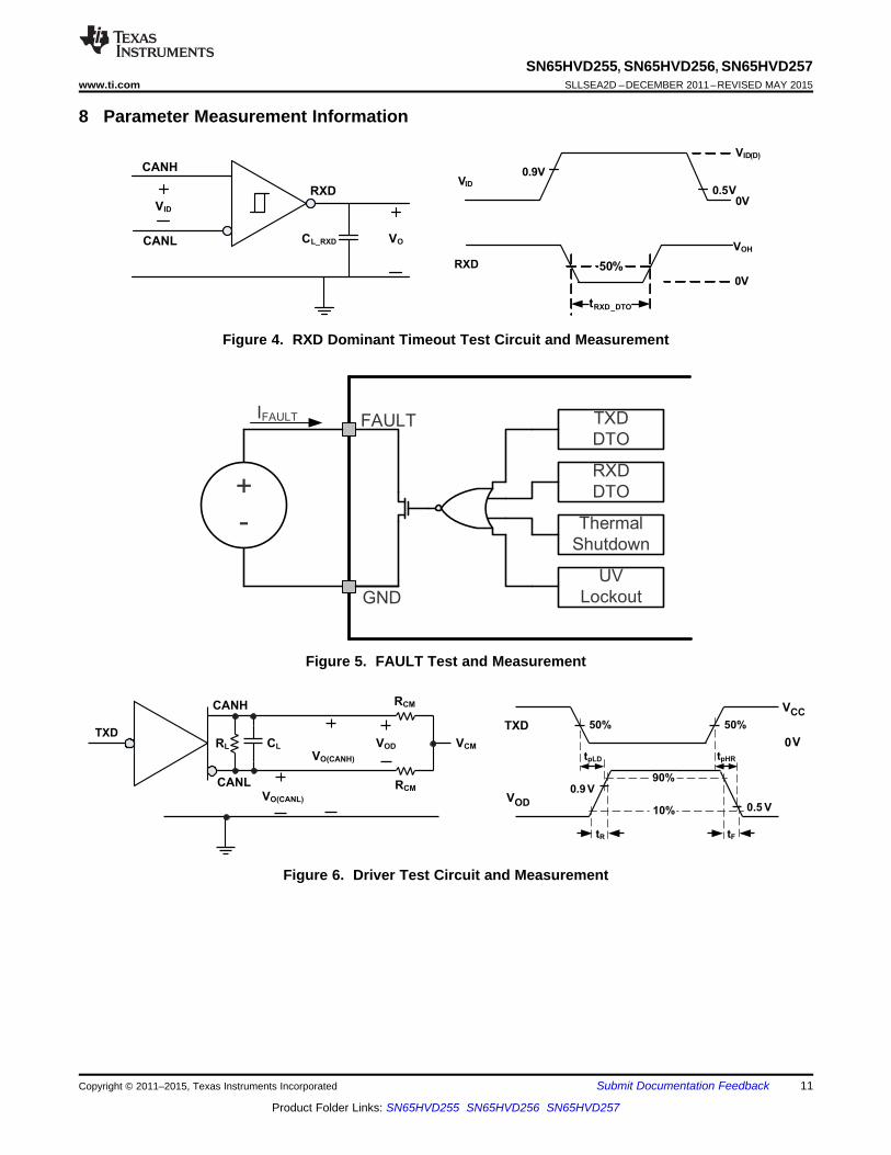
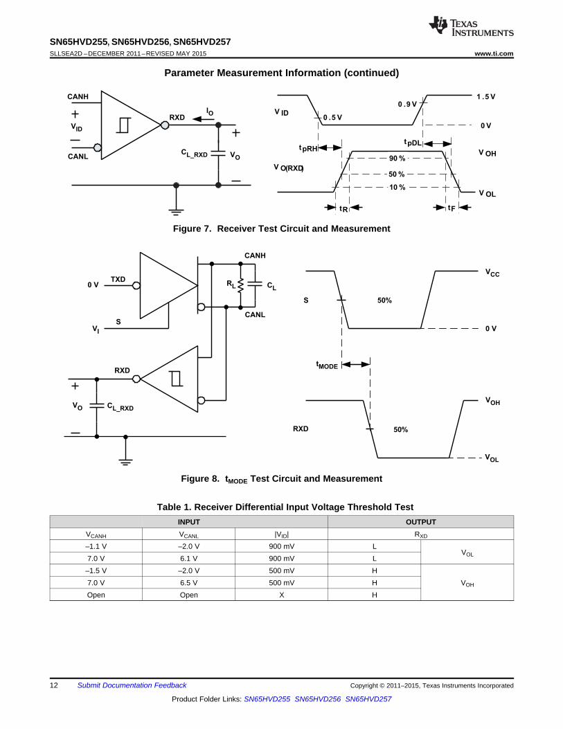
8 Parameter Measurement Information
Figure 4. RXD Dominant Timeout Test Circuit and Measurement
Figure 5. FAULT Test and Measurement
Figure 6. Driver Test Circuit and Measurement
Copyright © 2011–2015, Texas Instruments Incorporated Submit Documentation Feedback 11
Product Folder Links: SN65HVD255 SN65HVD256 SN65HVD257
CANH
CANL
TXDCL
VO CL_RXD
RXD
SVI
0 V
tMODE
S
RXD
VOH
VOL
VCC
50%
50%
RL
0 V
VOCL_RXD
CANH
RXD
CANL
VID
V ID0 .5 V
0 .9 V1 .5 V
0 V
V O(RXD)50 %
V OH
V OL
tpDLtpRH
90 %
10 %
tR tF
IO
SN65HVD255, SN65HVD256, SN65HVD257SLLSEA2D –DECEMBER 2011–REVISED MAY 2015 www.ti.com
Parameter Measurement Information (continued)
Figure 7. Receiver Test Circuit and Measurement
Figure 8. tMODE Test Circuit and Measurement
Table 1. Receiver Differential Input Voltage Threshold TestINPUT OUTPUT
VCANH VCANL |VID| RXD
–1.1 V –2.0 V 900 mV LVOL7.0 V 6.1 V 900 mV L
–1.5 V –2.0 V 500 mV H7.0 V 6.5 V 500 mV H VOH
Open Open X H
12 Submit Documentation Feedback Copyright © 2011–2015, Texas Instruments Incorporated
Product Folder Links: SN65HVD255 SN65HVD256 SN65HVD257

CANH
CANL
TXD
0 V
VBUS
IOS
or
200 sm
IOS
VBUS
VBUS
VBUS
0 V
VBUS
VOD
CANH
CANL
TXDCL
TXD
0.9 V
0.5 V
0V
VIH
tTXD_DTO
0 V
RL
VOD
VOD(D)
CANH
CANL
TXDCL
CL_RXD
RXD
S
VI
0 V
tPROP(LOOP1)
TXD
RXD
VOH
VOL
VCC
0 V
50%
50%
VO
RL
tPROP(LOOP2)
SN65HVD255, SN65HVD256, SN65HVD257www.ti.com SLLSEA2D –DECEMBER 2011–REVISED MAY 2015
Figure 9. TPROP(LOOP) Test Circuit and Measurement
Figure 10. TXD Dominant Timeout Test Circuit and Measurement
Figure 11. Driver Short Circuit Current Test and Measurement
Copyright © 2011–2015, Texas Instruments Incorporated Submit Documentation Feedback 13
Product Folder Links: SN65HVD255 SN65HVD256 SN65HVD257

VCC
CANH7
6CANL
RXD
1TXD
S8
DOMINANT
TIME OUT
OVERTEMPERATURE
LOGICOUTPUT
MODE SELECT
4
NC / VRXD / FAULT (See Note A) VCC
5 3
GND
2
UNDER
VOLTAGE
DOMINANTTIME OUT
(See Note B)
VCC
VCC or VRXD (See Note B)
FAULT LOGIC
MUX (See Note A)
SN65HVD255, SN65HVD256, SN65HVD257SLLSEA2D –DECEMBER 2011–REVISED MAY 2015 www.ti.com
9 Detailed Description
9.1 OverviewThe SN65HVD25x family of bus transceiver devices are compatible with the ISO 11898-2 High Speed CAN(Controller Area Network) physical layer standard. The SN65HVD25x devices are designed to interface betweenthe differential bus lines and the CAN protocol controller at data rates up to 1 Mbps (megabits per second).
9.2 Functional Block Diagram
A. Pin 5 function is device dependent; NC on SN65HVD255, VRXD for RXD output level-shifting device on theSN65HVD256 device, and FAULT Output on the SN65HVD257 device.
B. RXD logic output is driven to 5-V VCC on 5-V only supply devices (SN65HVD255, SN65HVD257) and driven to VRXDon output level-shifting device (SN65HVD256).
C. RXD (Receiver) Dominant State Time Out is a device dependent option available only on the SN65HVD257 device.
9.3 Feature Description
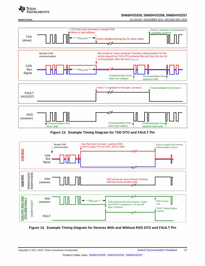
9.3.1 TXD Dominant Timeout (DTO)During normal mode (the only mode where the CAN driver is active), the TXD DTO circuit prevents thetransceiver from blocking network communication in the event of a hardware or software failure where TXD isheld dominant longer than the timeout period tTXD_DTO. The DTO circuit timer starts on a falling edge on TXD.The DTO circuit disables the CAN bus driver if no rising edge is seen before the timeout period expires, whichfrees the bus for communication between other nodes on the network. The CAN driver is reactivated when arecessive signal is seen on TXD pin, thus clearing the TXD DTO condition. The receiver and RXD pin still reflectthe CAN bus, and the bus pins are biased to recessive level during a TXD dominant timeout.
NOTEThe minimum dominant TXD time allowed by the TXD DTO circuit limits the minimumpossible transmitted data rate of the device. The CAN protocol allows a maximum ofeleven successive dominant bits (on TXD) for the worst case, where five successivedominant bits are followed immediately by an error frame. This, along with the tTXD_DTOminimum, limits the minimum data rate. Calculate the minimum transmitted data rate by:Minimum Data Rate = 11 / tTXD_DTO.
14 Submit Documentation Feedback Copyright © 2011–2015, Texas Instruments Incorporated
Product Folder Links: SN65HVD255 SN65HVD256 SN65HVD257
SN65HVD255, SN65HVD256, SN65HVD257www.ti.com SLLSEA2D –DECEMBER 2011–REVISED MAY 2015
Feature Description (continued)9.3.2 RXD Dominant Timeout (SN65HVD257)The SN65HVD257 device has a RXD dominant timeout (RXD DTO) circuit that prevents a bus stuck dominantfault from permanently driving the RXD output dominant (low) when the bus is held dominant longer than thetimeout period tRXD_DTO. The RXD DTO timer starts on a falling edge on RXD (bus going dominant). If no risingedge (bus returning recessive) is seen before the timeout constant of the circuit expires (tRXD_DTO), the RXD pinreturns high (recessive). The RXD output is reactivated to mirror the bus receiver output when a recessive signalis seen on the bus, clearing the RXD dominant timeout. The CAN bus pins are biased to the recessive levelduring a RXD DTO.
NOTEThe minimum dominant RXD time allowed by the RXD DTO limits the minimum possiblereceived data rate of the device. The CAN protocol allows a maximum of elevensuccessive dominant bits for the worst case transmission, where five successive dominantbits are followed immediately by an error frame. This, along with the tRXD_DTO minimum,limits the minimum data rate. The minimum received data rate may be calculated by:Minimum Data Rate = 11 / tRXD_DTO.
9.3.3 Thermal ShutdownIf the junction temperature of the device exceeds the thermal shut down threshold, the device turns off the CANdriver circuits thus blocking the TXD to bus transmission path. The shutdown condition is cleared when thejunction temperature drops below the thermal shutdown temperature of the device.
NOTEDuring thermal shutdown the CAN bus drivers turn off; thus, no transmission is possiblefrom TXD to the bus. The CAN bus pins are biased to recessive level during a thermalshutdown, and the receiver to RXD path remains operational.
9.3.4 Undervoltage LockoutThe supply pins have undervoltage detection that places the device in protected mode, which protects the busduring an undervoltage event on either the VCC or VRXD supply pins.
Table 2. Undervoltage Lockout 5-V Only Devices (SN65HVD255 and SN65HVD257)VCC DEVICE STATE BUS OUTPUT RXD
GOOD Normal Per Device State and TXD Mirrors BusBAD Protected High Impedance High Impedance (3-state)
Copyright © 2011–2015, Texas Instruments Incorporated Submit Documentation Feedback 15
Product Folder Links: SN65HVD255 SN65HVD256 SN65HVD257
TXD
DTO
RXD
DTO
Thermal
Shutdown
FAULT
GND
UV
Lockout
VCC or VIO
µP
FAULT
Input
SN65HVD255, SN65HVD256, SN65HVD257SLLSEA2D –DECEMBER 2011–REVISED MAY 2015 www.ti.com
Table 3. Undervoltage Lockout 5 V and VRXD Device (SN65HVD256)VCC VRXD DEVICE STATE BUS OUTPUT RXD
GOOD GOOD Normal Per Device State and TXD Mirrors BusBAD GOOD Protected High Impedance High (Recessive)
GOOD BAD Protected Recessive High Impedance (3-state)BAD BAD Protected High Impedance High Impedance (3-state)
NOTEAfter an undervoltage condition is cleared and the supplies have returned to valid levels,the device typically resumes normal operation in 300 µs.
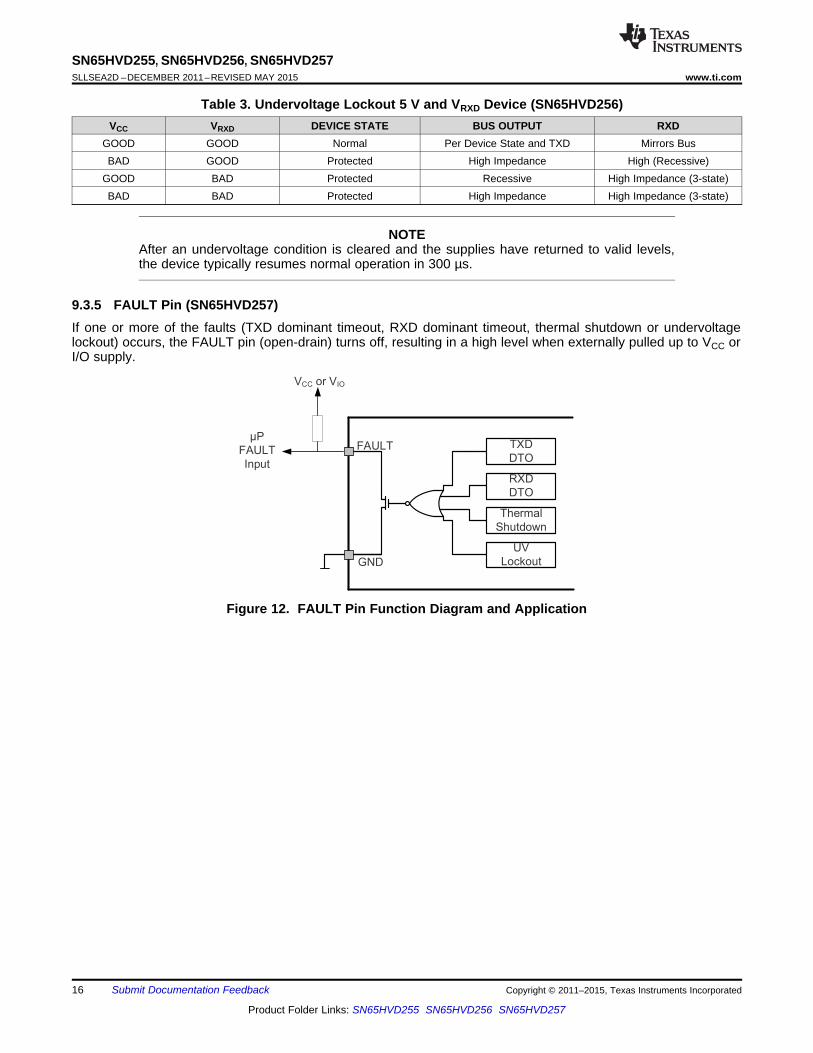
9.3.5 FAULT Pin (SN65HVD257)If one or more of the faults (TXD dominant timeout, RXD dominant timeout, thermal shutdown or undervoltagelockout) occurs, the FAULT pin (open-drain) turns off, resulting in a high level when externally pulled up to VCC orI/O supply.
Figure 12. FAULT Pin Function Diagram and Application
16 Submit Documentation Feedback Copyright © 2011–2015, Texas Instruments Incorporated
Product Folder Links: SN65HVD255 SN65HVD256 SN65HVD257
Normal CAN
communication
CAN
Bus
Signal
Bus Fault stuck dominant , example CANH
short to supply =5V and CAN L short to GND .
RXD output is returned recessive (high)
and FAULT is signaled to μP and link
layer / protocol.
RXD
(reciever)
RXD
(receiver)
tRXD_DTO
FAULT
CA
NP
HY
Wit
hR
XD
DT
OA
ND
FA
UL
T
SN
65
HV
D2
57
CA
NP
HY
SN
65
HV
D2
55
SN
65
HV
D2
56
Fault is repaired and normal
communication returns
FAULT cleared signal
is given
RXD mirrors
bus
RXD will also be “stuck dominant” blocking
alternative communication paths
CA
NB
US
Normal CAN communication
CAN Bus
Signal
TXD fault stuck dominant, example PCB failure or bad software
Fault is repaired & transmission capability restored
TXD (driver)
%XVZRXOGEH³VWXFNGRPLQDQW´EORFNLQJFRPPXQLFDWLRQIRUWKH
whole network but TXD DTO prevents this and frees the bus for communication after the time tTXD_DTO.
tTXD_DTO
Communication from local node
Communication from repaired node
RXD (receiver)
Communication from other bus node(s)
Communication from repaired local node
FAULT (HVD257)
Fault indication is removed. FAULT is signaled to link layer / protocol.
Communication from other bus node(s)
tTXD_DTO Driver disabled freeing bus for other nodes
SN65HVD255, SN65HVD256, SN65HVD257www.ti.com SLLSEA2D –DECEMBER 2011–REVISED MAY 2015
Figure 13. Example Timing Diagram for TXD DTO and FAULT Pin
Figure 14. Example Timing Diagram for Devices With and Without RXD DTO and FAULT Pin
Copyright © 2011–2015, Texas Instruments Incorporated Submit Documentation Feedback 17
Product Folder Links: SN65HVD255 SN65HVD256 SN65HVD257
SN65HVD255, SN65HVD256, SN65HVD257SLLSEA2D –DECEMBER 2011–REVISED MAY 2015 www.ti.com
9.3.6 Unpowered DeviceThe SN65HVD25x device is designed to be an ideal passive or no load to the CAN bus if it is unpowered. Thebus pins (CANH, CANL) have extremely low leakage currents when the device is unpowered, so they will notload down the bus. This is critical if some nodes of the network will be unpowered while the rest of the of networkremains in operation. The logic pins also have extremely low leakage currents when the device is unpowered toavoid loading down other circuits that may remain powered.
9.3.7 Floating PinsThe device has internal pullups and pulldowns on critical pins to place the device into known states if the pinsfloat. The TXD pin is pulled up to VCC to force a recessive input level if the pin floats. The S pin is pulled down toGND to force the device into normal mode if the pin floats.
9.3.8 CAN Bus Short-Circuit Current LimitingThe SN65HVD25x device has several protection features that limit the short circuit current when a CAN bus lineis shorted. These features include driver current limiting (dominant and recessive). The device has TXDdominant state time out to prevent permanent higher short circuit current of the dominant state during a systemfault. During CAN communication, the bus switches between dominant and recessive states with the data andcontrol fields bits; thus the short circuit current may be viewed either as the instantaneous current during eachbus state or as a DC average current. For system current (power supply) and power considerations in thetermination resistors and common-mode choke ratings, use the average short circuit current. Determine the ratioof dominant and recessive bits by the data in the CAN frame plus the following factors of the protocol and PHYthat force either recessive or dominant at the following times:
• Control fields with set bits• Bit stuffing• Interframe space• TXD dominant time out (fault case limiting)
These factors ensure a minimum recessive amount of time on the bus even if the data field contains a highpercentage of dominant bits.
18 Submit Documentation Feedback Copyright © 2011–2015, Texas Instruments Incorporated
Product Folder Links: SN65HVD255 SN65HVD256 SN65HVD257

SN65HVD255, SN65HVD256, SN65HVD257www.ti.com SLLSEA2D –DECEMBER 2011–REVISED MAY 2015
The short circuit current of the bus depends on the ratio of recessive to dominant bits and their respective shortcircuit currents. The average short circuit current may be calculated with Equation 1.
IOS(AVG) = %Transmit × [(%REC_Bits × IOS(SS)_REC) + (%DOM_Bits × IOS(SS)_DOM)] + [%Receive × IOS(SS)_REC] (1)
where:IOS(AVG) is the average short circuit current%Transmit is the percentage the node is transmitting CAN messages%Receive is the percentage the node is receiving CAN messages%REC_Bits is the percentage of recessive bits in the transmitted CAN messages%DOM_Bits is the percentage of dominant bits in the transmitted CAN messagesIOS(SS)_REC is the recessive steady state short circuit currentIOS(SS)_DOM is the dominant steady state short circuit current
NOTEConsider the short circuit current and possible fault cases of the network when sizing thepower ratings of the termination resistance and other network components.
9.4 Device Functional Modes
Table 4. Driver Function TableINPUTS OUTPUTS DRIVEN BUSDEVICE STATES (1) (2) TXD (1) (3) CANH (1) CANL (1)
L H L DominantL or Open
All Devices H or Open Z Z RecessiveH X Z Z Recessive
(1) H = high level, L = low level, X= irrelevant, Z = common mode (recessive) bias to VCC / 2. SeeFigure 15 and Figure 16 for bus state and common mode bias information.
(2) Devices have an internal pulldown to GND on S pin. If S pin is open the pin will be pulled low and thedevice will be in normal mode.
(3) Devices have an internal pullup to VCC on TXD pin. If the TXD pin is open the pin will be pulled highand the transmitter will remain in recessive (nondriven) state.
Table 5. Receiver Function TableCAN DIFFERENTIAL INPUTSDEVICE MODE BUS STATE RXD PIN (1)
VID = VCANH – VCANL
VID ≥ 0.9 V Dominant L (2)
0.5 V < VID < 0.9 V ? ?Normal or Silent
VID ≤ 0.5 V Recessive HOpen (VID ≈ 0 V) Open H
(1) H = high level, L = low level, ? = indeterminate.(2) RXD output remains dominant (low) as long as the bus is dominant. On the SN65HVD257 device with
RXD dominant timeout, when the bus has been dominant longer than the dominant timeout, tRXD_DTO,the RXD pin will return recessive (high). See RXD Dominant Timeout (SN65HVD257) for a descriptionof behavior during receiving a bus stuck dominant condition.
9.4.1 Operating ModesThe device has two main operating modes: normal mode and silent mode. Operating mode selection is made viathe S input pin.
Table 6. Operating ModesS Pin MODE DRIVER RECEIVER RXD PINLOW Normal Mode Enabled (ON) Enabled (ON) Mirrors Bus State (1)
HIGH Silent Mode Disabled (OFF) Enabled (ON) Mirrors Bus State
(1) Mirrors bus state: low if CAN bus is dominant, high if CAN bus is recessive.
Copyright © 2011–2015, Texas Instruments Incorporated Submit Documentation Feedback 19
Product Folder Links: SN65HVD255 SN65HVD256 SN65HVD257

RXD
CANH
CANL
V /2CC
Recessive
Logic H
Dominant
Logic L
Recessive
Logic H
Time, t
Ty
pic
al
Bu
sV
olt
ag
e(V
)
Normal & Silent Mode
CANL
CANH
Vdiff(D)
Vdiff(R)
4
3
2
1
SN65HVD255, SN65HVD256, SN65HVD257SLLSEA2D –DECEMBER 2011–REVISED MAY 2015 www.ti.com
9.4.2 Can Bus StatesThe CAN bus has two states during powered operation of the device: dominant and recessive. A dominant busstate is when the bus is driven differentially, corresponding to a logic low on the TXD and RXD pin. A recessivebus state is when the bus is biased to VCC / 2 via the high-resistance internal input resistors RIN of the receiver,corresponding to a logic high on the TXD and RXD pins. See Figure 15 and Figure 16.
Figure 15. Bus States (Physical Bit Representation)
Figure 16. Simplified Recessive Common Mode Bias and Receiver
9.4.3 Normal ModeSelect the normal mode of device operation by setting S low. The CAN driver and receiver are fully operationaland CAN communication is bidirectional. The driver is translating a digital input on TXD to a differential output onCANH and CANL. The receiver is translating the differential signal from CANH and CANL to a digital output onRXD.
9.4.4 Silent ModeActivate silent mode (receive only) by setting S high. The CAN driver is turned off while the receiver remainsactive and RXD outputs the received bus state.
NOTESilent mode may be used to implement babbling idiot protection, to ensure that the driverdoes not disrupt the network during a local fault. Silent mode may also be used inredundant systems to select or de-select the redundant transceiver (driver) when needed.
20 Submit Documentation Feedback Copyright © 2011–2015, Texas Instruments Incorporated
Product Folder Links: SN65HVD255 SN65HVD256 SN65HVD257
SN65HVD255, SN65HVD256, SN65HVD257www.ti.com SLLSEA2D –DECEMBER 2011–REVISED MAY 2015
9.4.5 Digital Inputs and Outputs
9.4.5.1 5-V VCC Only Devices (SN65HVD255 and SN65HVD257)The 5-V VCC device is supplied by a single 5-V rail. The digital inputs are 5-V and 3.3-V compatible. TheSN65HVD255 and SN65HVD257 devices have a 5-V (VCC) level RXD output. TXD is internally pulled up to VCCand S is internally pulled down to GND.
NOTETXD is internally pulled up to VCC and the S pin is internally pulled down to GND.However, the internal bias may only put the device into a known state if the pins float. Theinternal bias may be inadequate for system-level biasing. TXD pullup strength and CAN bittiming require special consideration when the SN65HVD25x devices are used with anopen-drain TXD output on the CAN controller. An adequate external pullup resistor mustbe used to ensure that the CAN controller output of the μP maintains adequate bit timinginput to the SN65HVD25x devices.
9.4.5.2 5-V VCC With VRXD RXD Output Supply Devices (SN65HVD256)This device is a 5-V VCC CAN transceiver with a separate supply for the RXD output, VRXD. The digital inputs are5-V and 3.3-V compatible. The SN65HVD256 device has a VRXD level RXD output. TXD remains weakly pulledup to VCC.
NOTEOn device versions with a VRXD supply that shifts the RXD output level, the input pins ofthe device remain the same. TXD remains weakly pulled up to VCC internally. Thus, asmall IIH current flows if the TXD input is used below VCC levels.
9.4.5.3 5-V VCC with FAULT Open-Drain Output Device (SN65HVD257)The SN65HVD257 device has a FAULT output pin (open-drain). FAULT must be pulled up to VCC or I/O supplylevel through an external resistor.
NOTEBecause the FAULT output pin is open-drain, it actively pulls down when there is no faultand becomes high-impedance when a fault condition is detected. An external pullupresistor to the VCC or I/O supply of the system must be used to pull the pin high to indicatea fault to the host microprocessor. The open-drain architecture makes the fault pincompatible with 3.3-V and 5-V I/O-level systems. The pullup current, selected by thepullup resistance value, must be as low as possible while achieving the desired voltagelevel output in the system with margin against noise.
Copyright © 2011–2015, Texas Instruments Incorporated Submit Documentation Feedback 21
Product Folder Links: SN65HVD255 SN65HVD256 SN65HVD257

SN65HVD255, SN65HVD256, SN65HVD257SLLSEA2D –DECEMBER 2011–REVISED MAY 2015 www.ti.com
10 Application and Implementation
NOTEInformation in the following applications sections is not part of the TI componentspecification, and TI does not warrant its accuracy or completeness. TI’s customers areresponsible for determining suitability of components for their purposes. Customers shouldvalidate and test their design implementation to confirm system functionality.
10.1 Application Information
10.1.1 Bus Loading, Length, and Number of NodesThe ISO 11898 standard states that a CAN bus should have a maximum of 30 nodes, be less than 40 metersfrom end to end, and should have no stubs greater than 0.3 meters. However, with careful design, users canhave longer cables, longer stub lengths, and many more nodes to a bus. A large number of nodes requires atransceiver with high input impedance, such as the SN65HVD25x family devices.
Many CAN organizations and standards have scaled the use of CAN for applications outside the originalISO11898 standard. They have made system level trade-offs for data rate, cable length, and parasitic loading ofthe bus. Examples of some of these specifications are: ARINC825, CANopen, DeviceNet, and NMEA200.
A CAN network design is a series of trade-offs, but these devices operate over wide common-mode range. InISO11898-2, the driver differential output is specified with a 60-Ω load (the two 120-Ω termination resistors inparallel) and the differential output must be greater than 1.5 V. The SN65HVD25x devices are specified to meetthe 1.5-V requirement with a 45-Ω load incorporating the worst case including parallel transceivers. Thedifferential input resistance of the SN65HVD25x devices is a minimum of 30 KΩ. If 167 SN65HVD25x familytransceivers are in parallel on a bus, this is equivalent to a 180-Ω differential load worst case. That transceiverload of 180 Ω in parallel with the 60 Ω gives a total 45 Ω. Therefore, the SN65HVD25x family theoreticallysupports over 167 transceivers on a single bus segment with margin to the 1.2-V minimum differential input ateach node. However, CAN network design margin must be given for signal loss across the system and cabling,parasitic loadings, network imbalances, ground offsets, and signal integrity; thus a practical maximum number ofnodes is typically much lower. Bus length may also be extended beyond the original ISO11898 standard of 40 mby careful system design and data-rate tradeoffs. For example, CAN open network design guidelines allow thenetwork to be up to 1 km with changes in the termination resistance, cabling, less than 64 nodes, and asignificantly lowered data rate.
This flexibility in CAN network design is one of the key strengths of the various extensions and additionalstandards that have been built on the original ISO11898 CAN standard. In using this flexibility comes theresponsibility of good network design and balancing these tradeoffs.
22 Submit Documentation Feedback Copyright © 2011–2015, Texas Instruments Incorporated
Product Folder Links: SN65HVD255 SN65HVD256 SN65HVD257
MCU or DSP
CANController
CANTransceiver
Node 1
MCU or DSP
CANController
CANTransceiver
Node 2
MCU or DSP
CANController
CANTransceiver
Node 3
MCU or DSP
CANController
CANTransceiver
Node n
(with termination)
RTERM
RTERM
5-V MCU SN65HVD255CAN Transceiver
S
RXD
TXD
CANH
CANL
Port x
RXD
TXD
VCC
8
1
4
2
37
56
5-V VoltageRegulator
(e.g.TPSxxxx)
VOUT
GNDNC
VIN
VIN
VCC
SN65HVD255, SN65HVD256, SN65HVD257www.ti.com SLLSEA2D –DECEMBER 2011–REVISED MAY 2015
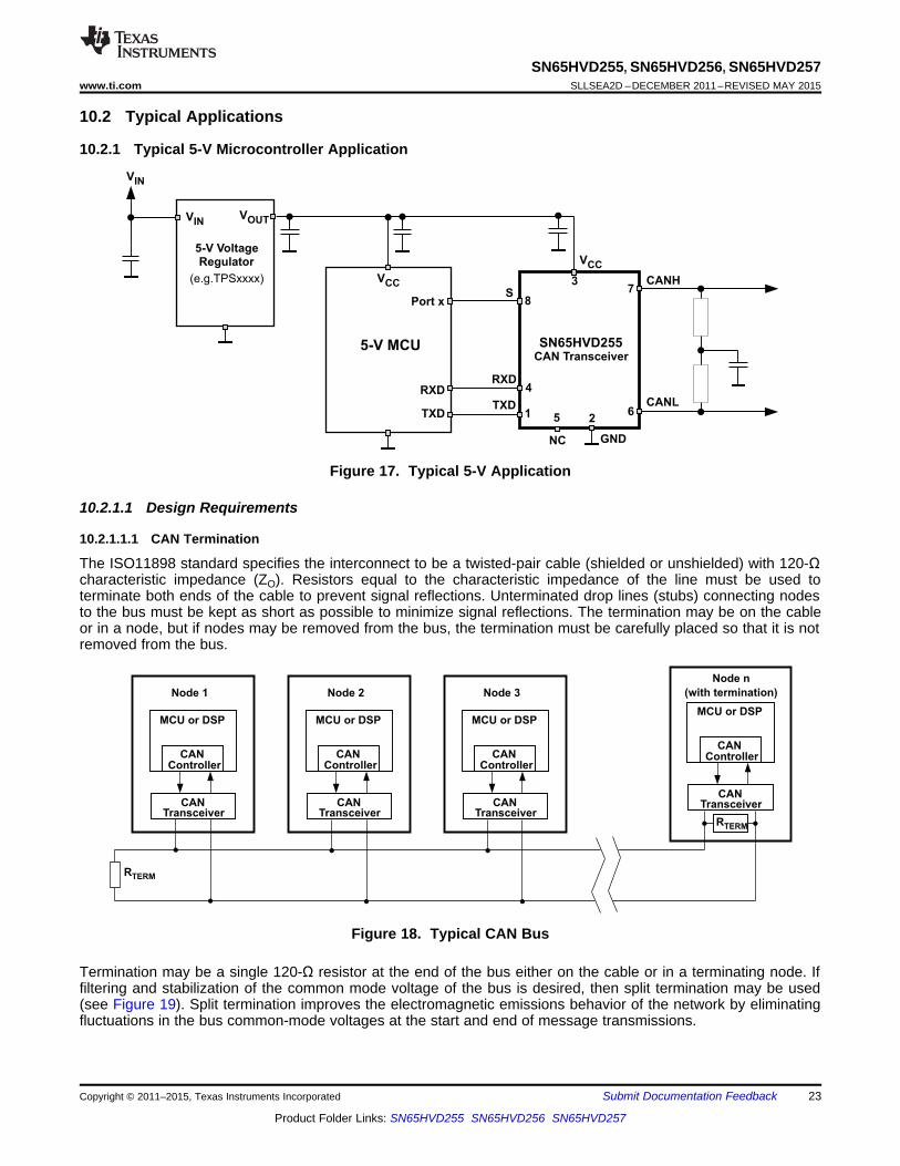
10.2 Typical Applications
10.2.1 Typical 5-V Microcontroller Application
Figure 17. Typical 5-V Application
10.2.1.1 Design Requirements
10.2.1.1.1 CAN Termination
The ISO11898 standard specifies the interconnect to be a twisted-pair cable (shielded or unshielded) with 120-Ωcharacteristic impedance (ZO). Resistors equal to the characteristic impedance of the line must be used toterminate both ends of the cable to prevent signal reflections. Unterminated drop lines (stubs) connecting nodesto the bus must be kept as short as possible to minimize signal reflections. The termination may be on the cableor in a node, but if nodes may be removed from the bus, the termination must be carefully placed so that it is notremoved from the bus.
Figure 18. Typical CAN Bus
Termination may be a single 120-Ω resistor at the end of the bus either on the cable or in a terminating node. Iffiltering and stabilization of the common mode voltage of the bus is desired, then split termination may be used(see Figure 19). Split termination improves the electromagnetic emissions behavior of the network by eliminatingfluctuations in the bus common-mode voltages at the start and end of message transmissions.
Copyright © 2011–2015, Texas Instruments Incorporated Submit Documentation Feedback 23
Product Folder Links: SN65HVD255 SN65HVD256 SN65HVD257

CAN
Transceiver
CANL
CANH
CSPLIT
CAN
TransceiverRTERM
Standard Termination Split Termination
CANL
CANH
R /2TERM
R /2TERM
SN65HVD255, SN65HVD256, SN65HVD257SLLSEA2D –DECEMBER 2011–REVISED MAY 2015 www.ti.com
Typical Applications (continued)
Figure 19. CAN Bus Termination Concepts
10.2.1.2 Detailed Design Procedure
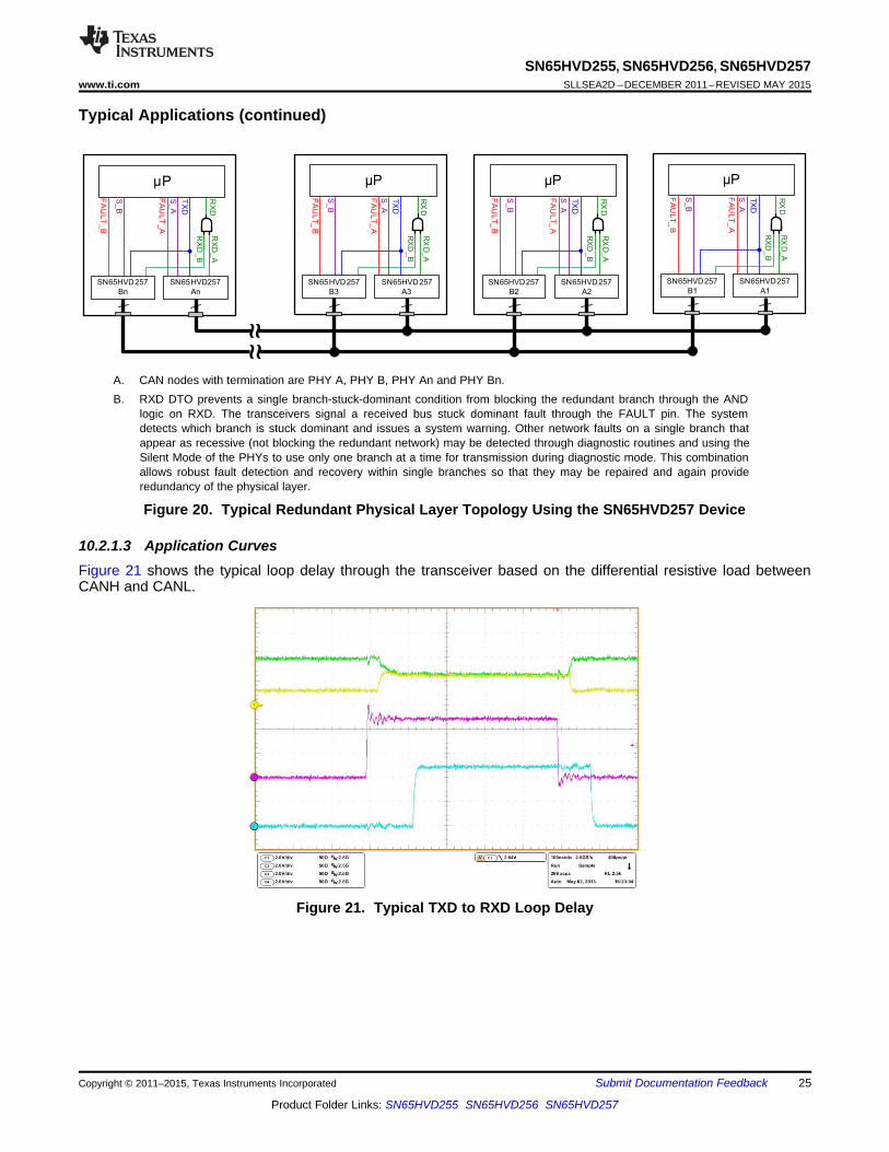
10.2.1.2.1 Example: Functional Safety Using the SN65HVD257 in a Redundant Physical Layer CAN NetworkTopology
CAN is a standard linear bus topology using 120-Ω twisted-pair cabling. The SN65HVD257 CAN device includesseveral features to use the CAN physical layer in nonstandard topologies with only one CAN link layer controller(μP) interface. This allows much greater flexibility in the physical topology of the bus while reducing the digitalcontroller and software costs. The combination of RXD DTO and the FAULT output allows great flexibility,control, and monitoring of these applications.
A simple example of this flexibility is to use two SN65HVD257 devices in parallel with an AND gate to achieveredundancy (parallel) of the physical layer (cabling and PHYs) in a CAN network.
For the CAN bit-wise arbitration to work, the RXD outputs of the transceivers must connect through AND gatelogic so that a dominant bit (low) from any of the branches is received by the link layer logic (μP) and appears tothe link layer and above as a single physical network. The RXD DTO feature prevents a bus stuck dominant faultin a single branch from taking down the entire network by forcing the RXD pin for the transceivers on the branchwith the fault back to the recessive after the tRXD_DTO time. The remaining branch of the network continues tofunction. The FAULT pin of the transceivers on the branch with the fault indicates this through the FAULT outputto their host processors, which diagnose the failure condition. The S pin (silent mode pin) may be used to put abranch in silent mode to check each branch for other faults. Therefore, it is possible to implement a robust andredundant CAN network topology in a very simple and low-cost manner.
These concepts can be expanded into more complicated and flexible CAN network topologies to solve varioussystem-level challenges with a networked infrastructure.
24 Submit Documentation Feedback Copyright © 2011–2015, Texas Instruments Incorporated
Product Folder Links: SN65HVD255 SN65HVD256 SN65HVD257
~~ ~
~
μP
SN65HVD257
An
RX
D_A
TX
D
FA
ULT
_A
RX
D
RX
D_B
SN65HVD257
Bn
FA
ULT
_B
S_B
S_A
μP
SN65HVD257
A3
RX
D_A
TX
D
FA
ULT_
A
RX
D
RX
D_B
SN65HVD257
B3
FA
ULT_
B
S_B
S_A
μP
SN65HVD257
A2R
XD
_A
TX
D
FA
ULT_
A
RX
D
RX
D_B
SN65HVD257
B2
FA
ULT_
B
S_B
S_A
μP
SN65HVD257
A1
RX
D_A
TX
D
FA
ULT_
A
RX
D
RX
D_B
SN65HVD257
B1
FA
ULT_
B
S_B
S_A
SN65HVD255, SN65HVD256, SN65HVD257www.ti.com SLLSEA2D –DECEMBER 2011–REVISED MAY 2015
Typical Applications (continued)
A. CAN nodes with termination are PHY A, PHY B, PHY An and PHY Bn.B. RXD DTO prevents a single branch-stuck-dominant condition from blocking the redundant branch through the AND
logic on RXD. The transceivers signal a received bus stuck dominant fault through the FAULT pin. The systemdetects which branch is stuck dominant and issues a system warning. Other network faults on a single branch thatappear as recessive (not blocking the redundant network) may be detected through diagnostic routines and using theSilent Mode of the PHYs to use only one branch at a time for transmission during diagnostic mode. This combinationallows robust fault detection and recovery within single branches so that they may be repaired and again provideredundancy of the physical layer.
Figure 20. Typical Redundant Physical Layer Topology Using the SN65HVD257 Device
10.2.1.3 Application CurvesFigure 21 shows the typical loop delay through the transceiver based on the differential resistive load betweenCANH and CANL.
Figure 21. Typical TXD to RXD Loop Delay
Copyright © 2011–2015, Texas Instruments Incorporated Submit Documentation Feedback 25
Product Folder Links: SN65HVD255 SN65HVD256 SN65HVD257
3-V MCU SN65HVD256
CAN Transceiver
S
RXD
TXD
CANH
CANL
Port x
RXD
TXD
VCC
8
1
4
2
37
56
5-V Voltage
Regulator
(e.g. TPSxxxx)
VOUT
GNDVRXD
VIN
3-V VoltageRegulator
VIN
VOUTVIN
(e.g. TPSxxxx)
VCC
SN65HVD255, SN65HVD256, SN65HVD257SLLSEA2D –DECEMBER 2011–REVISED MAY 2015 www.ti.com
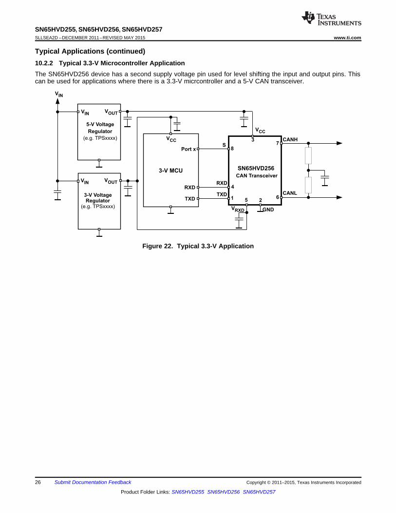
Typical Applications (continued)10.2.2 Typical 3.3-V Microcontroller ApplicationThe SN65HVD256 device has a second supply voltage pin used for level shifting the input and output pins. Thiscan be used for applications where there is a 3.3-V micrcontroller and a 5-V CAN transceiver.
Figure 22. Typical 3.3-V Application
26 Submit Documentation Feedback Copyright © 2011–2015, Texas Instruments Incorporated
Product Folder Links: SN65HVD255 SN65HVD256 SN65HVD257
SN65HVD255, SN65HVD256, SN65HVD257www.ti.com SLLSEA2D –DECEMBER 2011–REVISED MAY 2015
11 Power Supply RecommendationsTo ensure reliable operation at all data rates and supply voltages, each supply must be decoupled with a 100-nFceramic capacitor located as close as possible to the supply pins. The TPS76350 device is a linear voltageregulator suitable for the 5-V supply rail.
12 Layout
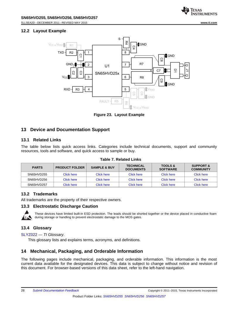
12.1 Layout GuidelinesFor the PCB design to be successful, start with the design of the protection and filtering circuitry because ESDand EFT transients have a wide frequency bandwidth from approximately 3-MHz to 3-GHz and high frequencylayout techniques must be applied during PCB design. On chip IEC ESD protection is good for laboratory andportable equipment but is usually not sufficient for EFT and surge transients occurring in industrial environments.Therefore, robust and reliable bus node design requires the use of external transient protection devices at thebus connectors. Placement at the connector also prevents these harsh transient events from propagating furtherinto the PCB and system.
Use VCC and ground planes to provide low inductance.
NOTEHigh frequency current follows the path of least inductance and not the path of leastresistance.
Design the bus protection components in the direction of the signal path. Do not force the transient current todivert from the signal path to reach the protection device. Below is a list of layout recommendations whendesigning a CAN transceiver into an application.• Transient Protection on CANH and CANL: Transient Voltage Suppression (TVS) and capacitors (D1, C5
and C7 shown in Figure 23) can be used to protect the system level transients like EFT, IEC ESD, andSurge. These devices must be placed as close to the connector as possible. This prevents the transientenergy and noise from penetrating into other nets on the board.
• Bus Termination on CANH and CANL: Figure 23 shows split termination where the termination is split intotwo resistors, R5 and R6, with the center or split tap of the termination connected to ground through capacitorC6. Split termination provides common mode filtering for the bus. When termination is placed on the boardinstead of directly on the bus, care must be taken to ensure the terminating node is not removed from thebus, as this causes signal integrity issues if the bus is not properly terminated on both ends.
• Decoupling Capacitors on VCC and VRXD: Bypass and bulk capacitors must be placed as close as possibleto the supply pins of transceiver (examples are C2, C3, C5, and C6).
• Ground and power connections: Use at least two vias for VCC, VIO, and ground connections of bypasscapacitors and protection devices to minimize trace and via inductance.
• Digital inputs and outputs: To limit current of digital lines, serial resistors may be used. Examples are R1,R2, R3, R4, and R5.
• Filtering noise on digital inputs and outputs: To filter noise on the digital I/O lines, a capacitor may beused close to the input side of the I/O as shown by C1 and C4.
• External pull-up resistors on input and output pins: Because the internal pullup and pulldown biasing ofthe device is weak for floating pins, an external 1-kΩ to 10-kΩ pullup or pulldown resistor must be used tobias the state of the pins during transient events.
• Fault Output Pin (SN65HVD257 only): Because the FAULT output pin is an open drain output, an externalpullup resistor is required to pull the pin voltage high for normal operation (R5).
• VRXD Supply (SN65HVD256 only): The SN65HVD256 device will need additional bypass capacitors for theVRXD supply shown with C5 and C6.
• TXD input pin: If an open-drain host processor is used to drive the TXD pin of the device, an external pullupresistor between 1 kΩ and 10 kΩ must be used to help drive the recessive input state of the device (weakinternal pullup resistor).
Copyright © 2011–2015, Texas Instruments Incorporated Submit Documentation Feedback 27
Product Folder Links: SN65HVD255 SN65HVD256 SN65HVD257
GND
J1U1
1
2
3
4
U1
SN65HVD25x
R3
R2
RXD
C3
VCC
C1
TXD
C7C2
7
6
5 C5
GNDC
6
S
8
GND
GND
R4
R8
R7
C8
C9
D1
R6FAULT
C4
GND
VRXD
VCC orVRXD
R5
VCC orVRXD R1
SN65HVD255, SN65HVD256, SN65HVD257SLLSEA2D –DECEMBER 2011–REVISED MAY 2015 www.ti.com
12.2 Layout Example
Figure 23. Layout Example
13 Device and Documentation Support
13.1 Related LinksThe table below lists quick access links. Categories include technical documents, support and communityresources, tools and software, and quick access to sample or buy.
Table 7. Related LinksTECHNICAL TOOLS & SUPPORT &PARTS PRODUCT FOLDER SAMPLE & BUY DOCUMENTS SOFTWARE COMMUNITY
SN65HVD255 Click here Click here Click here Click here Click hereSN65HVD256 Click here Click here Click here Click here Click hereSN65HVD257 Click here Click here Click here Click here Click here
13.2 TrademarksAll trademarks are the property of their respective owners.
13.3 Electrostatic Discharge CautionThese devices have limited built-in ESD protection. The leads should be shorted together or the device placed in conductive foamduring storage or handling to prevent electrostatic damage to the MOS gates.
13.4 GlossarySLYZ022 — TI Glossary.
This glossary lists and explains terms, acronyms, and definitions.
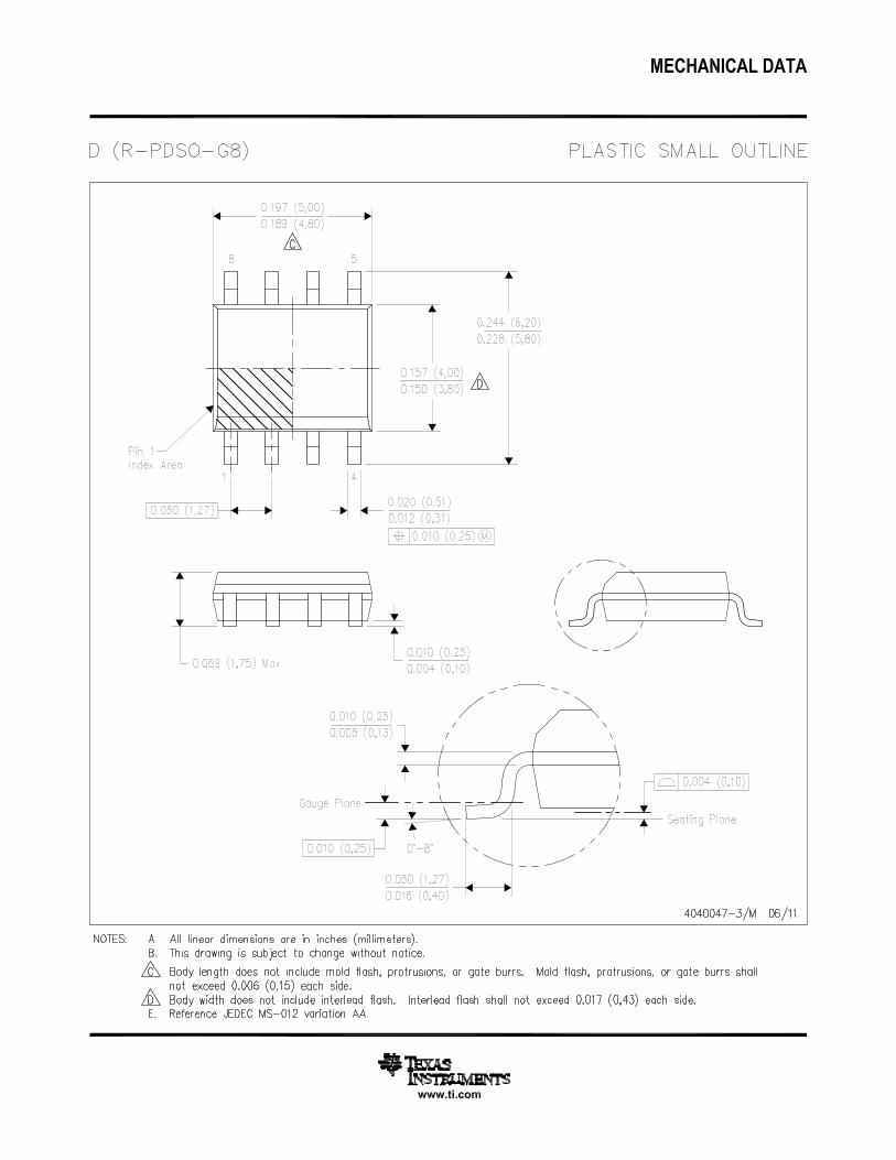
14 Mechanical, Packaging, and Orderable InformationThe following pages include mechanical, packaging, and orderable information. This information is the mostcurrent data available for the designated devices. This data is subject to change without notice and revision ofthis document. For browser-based versions of this data sheet, refer to the left-hand navigation.
28 Submit Documentation Feedback Copyright © 2011–2015, Texas Instruments Incorporated
Product Folder Links: SN65HVD255 SN65HVD256 SN65HVD257

PACKAGE OPTION ADDENDUM
www.ti.com 19-Mar-2015
Addendum-Page 1
PACKAGING INFORMATION
Orderable Device Status(1)
Package Type PackageDrawing
Pins PackageQty
Eco Plan(2)
Lead/Ball Finish(6)
MSL Peak Temp(3)
Op Temp (°C) Device Marking(4/5)
Samples
SN65HVD255D ACTIVE SOIC D 8 75 Green (RoHS& no Sb/Br)
CU NIPDAU Level-1-260C-UNLIM -40 to 125 HVD255
SN65HVD255DR ACTIVE SOIC D 8 2500 Green (RoHS& no Sb/Br)
CU NIPDAU Level-1-260C-UNLIM -40 to 125 HVD255
SN65HVD256D ACTIVE SOIC D 8 75 Green (RoHS& no Sb/Br)
CU NIPDAU Level-1-260C-UNLIM -40 to 125 HVD256
SN65HVD256DR ACTIVE SOIC D 8 2500 Green (RoHS& no Sb/Br)
CU NIPDAU Level-1-260C-UNLIM -40 to 125 HVD256
SN65HVD257D ACTIVE SOIC D 8 75 Green (RoHS& no Sb/Br)
CU NIPDAU Level-1-260C-UNLIM -40 to 125 HVD257
SN65HVD257DR ACTIVE SOIC D 8 2500 Green (RoHS& no Sb/Br)
CU NIPDAU Level-1-260C-UNLIM -40 to 125 HVD257
(1) The marketing status values are defined as follows:ACTIVE: Product device recommended for new designs.LIFEBUY: TI has announced that the device will be discontinued, and a lifetime-buy period is in effect.NRND: Not recommended for new designs. Device is in production to support existing customers, but TI does not recommend using this part in a new design.PREVIEW: Device has been announced but is not in production. Samples may or may not be available.OBSOLETE: TI has discontinued the production of the device.
(2) Eco Plan - The planned eco-friendly classification: Pb-Free (RoHS), Pb-Free (RoHS Exempt), or Green (RoHS & no Sb/Br) - please check http://www.ti.com/productcontent for the latest availabilityinformation and additional product content details.TBD: The Pb-Free/Green conversion plan has not been defined.Pb-Free (RoHS): TI's terms "Lead-Free" or "Pb-Free" mean semiconductor products that are compatible with the current RoHS requirements for all 6 substances, including the requirement thatlead not exceed 0.1% by weight in homogeneous materials. Where designed to be soldered at high temperatures, TI Pb-Free products are suitable for use in specified lead-free processes.Pb-Free (RoHS Exempt): This component has a RoHS exemption for either 1) lead-based flip-chip solder bumps used between the die and package, or 2) lead-based die adhesive used betweenthe die and leadframe. The component is otherwise considered Pb-Free (RoHS compatible) as defined above.Green (RoHS & no Sb/Br): TI defines "Green" to mean Pb-Free (RoHS compatible), and free of Bromine (Br) and Antimony (Sb) based flame retardants (Br or Sb do not exceed 0.1% by weightin homogeneous material)
(3) MSL, Peak Temp. - The Moisture Sensitivity Level rating according to the JEDEC industry standard classifications, and peak solder temperature.
(4) There may be additional marking, which relates to the logo, the lot trace code information, or the environmental category on the device.
(5) Multiple Device Markings will be inside parentheses. Only one Device Marking contained in parentheses and separated by a "~" will appear on a device. If a line is indented then it is a continuationof the previous line and the two combined represent the entire Device Marking for that device.
PACKAGE OPTION ADDENDUM
www.ti.com 19-Mar-2015
Addendum-Page 2
(6) Lead/Ball Finish - Orderable Devices may have multiple material finish options. Finish options are separated by a vertical ruled line. Lead/Ball Finish values may wrap to two lines if the finishvalue exceeds the maximum column width.
Important Information and Disclaimer:The information provided on this page represents TI's knowledge and belief as of the date that it is provided. TI bases its knowledge and belief on informationprovided by third parties, and makes no representation or warranty as to the accuracy of such information. Efforts are underway to better integrate information from third parties. TI has taken andcontinues to take reasonable steps to provide representative and accurate information but may not have conducted destructive testing or chemical analysis on incoming materials and chemicals.TI and TI suppliers consider certain information to be proprietary, and thus CAS numbers and other limited information may not be available for release.
In no event shall TI's liability arising out of such information exceed the total purchase price of the TI part(s) at issue in this document sold by TI to Customer on an annual basis.

TAPE AND REEL INFORMATION
*All dimensions are nominal
Device PackageType
PackageDrawing
Pins SPQ ReelDiameter
(mm)
ReelWidth
W1 (mm)
A0(mm)
B0(mm)
K0(mm)
P1(mm)
W(mm)
Pin1Quadrant
SN65HVD255DR SOIC D 8 2500 330.0 12.4 6.4 5.2 2.1 8.0 12.0 Q1
SN65HVD256DR SOIC D 8 2500 330.0 12.4 6.4 5.2 2.1 8.0 12.0 Q1
SN65HVD257DR SOIC D 8 2500 330.0 12.4 6.4 5.2 2.1 8.0 12.0 Q1
PACKAGE MATERIALS INFORMATION
www.ti.com 19-Mar-2015
Pack Materials-Page 1

*All dimensions are nominal
Device Package Type Package Drawing Pins SPQ Length (mm) Width (mm) Height (mm)
SN65HVD255DR SOIC D 8 2500 340.5 338.1 20.6
SN65HVD256DR SOIC D 8 2500 340.5 338.1 20.6
SN65HVD257DR SOIC D 8 2500 340.5 338.1 20.6
PACKAGE MATERIALS INFORMATION
www.ti.com 19-Mar-2015
Pack Materials-Page 2

IMPORTANT NOTICE
Texas Instruments Incorporated (TI) reserves the right to make corrections, enhancements, improvements and other changes to itssemiconductor products and services per JESD46, latest issue, and to discontinue any product or service per JESD48, latest issue. Buyersshould obtain the latest relevant information before placing orders and should verify that such information is current and complete.TI’s published terms of sale for semiconductor products (http://www.ti.com/sc/docs/stdterms.htm) apply to the sale of packaged integratedcircuit products that TI has qualified and released to market. Additional terms may apply to the use or sale of other types of TI products andservices.Reproduction of significant portions of TI information in TI data sheets is permissible only if reproduction is without alteration and isaccompanied by all associated warranties, conditions, limitations, and notices. TI is not responsible or liable for such reproduceddocumentation. Information of third parties may be subject to additional restrictions. Resale of TI products or services with statementsdifferent from or beyond the parameters stated by TI for that product or service voids all express and any implied warranties for theassociated TI product or service and is an unfair and deceptive business practice. TI is not responsible or liable for any such statements.Buyers and others who are developing systems that incorporate TI products (collectively, “Designers”) understand and agree that Designersremain responsible for using their independent analysis, evaluation and judgment in designing their applications and that Designers havefull and exclusive responsibility to assure the safety of Designers' applications and compliance of their applications (and of all TI productsused in or for Designers’ applications) with all applicable regulations, laws and other applicable requirements. Designer represents that, withrespect to their applications, Designer has all the necessary expertise to create and implement safeguards that (1) anticipate dangerousconsequences of failures, (2) monitor failures and their consequences, and (3) lessen the likelihood of failures that might cause harm andtake appropriate actions. Designer agrees that prior to using or distributing any applications that include TI products, Designer willthoroughly test such applications and the functionality of such TI products as used in such applications.TI’s provision of technical, application or other design advice, quality characterization, reliability data or other services or information,including, but not limited to, reference designs and materials relating to evaluation modules, (collectively, “TI Resources”) are intended toassist designers who are developing applications that incorporate TI products; by downloading, accessing or using TI Resources in anyway, Designer (individually or, if Designer is acting on behalf of a company, Designer’s company) agrees to use any particular TI Resourcesolely for this purpose and subject to the terms of this Notice.TI’s provision of TI Resources does not expand or otherwise alter TI’s applicable published warranties or warranty disclaimers for TIproducts, and no additional obligations or liabilities arise from TI providing such TI Resources. TI reserves the right to make corrections,enhancements, improvements and other changes to its TI Resources. TI has not conducted any testing other than that specificallydescribed in the published documentation for a particular TI Resource.Designer is authorized to use, copy and modify any individual TI Resource only in connection with the development of applications thatinclude the TI product(s) identified in such TI Resource. NO OTHER LICENSE, EXPRESS OR IMPLIED, BY ESTOPPEL OR OTHERWISETO ANY OTHER TI INTELLECTUAL PROPERTY RIGHT, AND NO LICENSE TO ANY TECHNOLOGY OR INTELLECTUAL PROPERTYRIGHT OF TI OR ANY THIRD PARTY IS GRANTED HEREIN, including but not limited to any patent right, copyright, mask work right, orother intellectual property right relating to any combination, machine, or process in which TI products or services are used. Informationregarding or referencing third-party products or services does not constitute a license to use such products or services, or a warranty orendorsement thereof. Use of TI Resources may require a license from a third party under the patents or other intellectual property of thethird party, or a license from TI under the patents or other intellectual property of TI.TI RESOURCES ARE PROVIDED “AS IS” AND WITH ALL FAULTS. TI DISCLAIMS ALL OTHER WARRANTIES ORREPRESENTATIONS, EXPRESS OR IMPLIED, REGARDING RESOURCES OR USE THEREOF, INCLUDING BUT NOT LIMITED TOACCURACY OR COMPLETENESS, TITLE, ANY EPIDEMIC FAILURE WARRANTY AND ANY IMPLIED WARRANTIES OFMERCHANTABILITY, FITNESS FOR A PARTICULAR PURPOSE, AND NON-INFRINGEMENT OF ANY THIRD PARTY INTELLECTUALPROPERTY RIGHTS. TI SHALL NOT BE LIABLE FOR AND SHALL NOT DEFEND OR INDEMNIFY DESIGNER AGAINST ANY CLAIM,INCLUDING BUT NOT LIMITED TO ANY INFRINGEMENT CLAIM THAT RELATES TO OR IS BASED ON ANY COMBINATION OFPRODUCTS EVEN IF DESCRIBED IN TI RESOURCES OR OTHERWISE. IN NO EVENT SHALL TI BE LIABLE FOR ANY ACTUAL,DIRECT, SPECIAL, COLLATERAL, INDIRECT, PUNITIVE, INCIDENTAL, CONSEQUENTIAL OR EXEMPLARY DAMAGES INCONNECTION WITH OR ARISING OUT OF TI RESOURCES OR USE THEREOF, AND REGARDLESS OF WHETHER TI HAS BEENADVISED OF THE POSSIBILITY OF SUCH DAMAGES.Unless TI has explicitly designated an individual product as meeting the requirements of a particular industry standard (e.g., ISO/TS 16949and ISO 26262), TI is not responsible for any failure to meet such industry standard requirements.Where TI specifically promotes products as facilitating functional safety or as compliant with industry functional safety standards, suchproducts are intended to help enable customers to design and create their own applications that meet applicable functional safety standardsand requirements. Using products in an application does not by itself establish any safety features in the application. Designers mustensure compliance with safety-related requirements and standards applicable to their applications. Designer may not use any TI products inlife-critical medical equipment unless authorized officers of the parties have executed a special contract specifically governing such use.Life-critical medical equipment is medical equipment where failure of such equipment would cause serious bodily injury or death (e.g., lifesupport, pacemakers, defibrillators, heart pumps, neurostimulators, and implantables). Such equipment includes, without limitation, allmedical devices identified by the U.S. Food and Drug Administration as Class III devices and equivalent classifications outside the U.S.TI may expressly designate certain products as completing a particular qualification (e.g., Q100, Military Grade, or Enhanced Product).Designers agree that it has the necessary expertise to select the product with the appropriate qualification designation for their applicationsand that proper product selection is at Designers’ own risk. Designers are solely responsible for compliance with all legal and regulatoryrequirements in connection with such selection.Designer will fully indemnify TI and its representatives against any damages, costs, losses, and/or liabilities arising out of Designer’s non-compliance with the terms and provisions of this Notice.
Mailing Address: Texas Instruments, Post Office Box 655303, Dallas, Texas 75265Copyright © 2017, Texas Instruments Incorporated