sn65hvd230m-ep - texas instruments · sgls356 − may 2006 2 description the sn65hvd230m...
TRANSCRIPT

SGLS356 − MAY 2006
1www.ti.com
FEATURES
Controlled Baseline− One Assembly/Test Site, One Fabrication
Site
Extended Temperature Performance of −55 °Cto 125°C
Enhanced Diminishing ManufacturingSources (DMS) Support
Enhanced Product-Change Notification
Qualification Pedigree †
Operates With a 3.3-V Supply
Low Power Replacement for the PCA82C250Footprint
Bus/Pin ESD Protection Exceeds 15-kV HBM
Controlled Driver Output Transition Times forImproved Signal Quality on theSN65HVD230M
Unpowered Node Does Not Disturb the Bus
Compatible With the Requirements of the ISO 11898 Standard
Low-Current SN65HVD230M Standby Mode370 µA Typical
Designed for Signaling Rates ‡ Up To1 Megabit/Second (Mbps)
Thermal Shutdown Protection
Open-Circuit Fail-Safe Design† Component qualification in accordance with JEDEC and industry
standards to ensure reliable operation over an extendedtemperature range. This includes, but is not limited to, HighlyAccelerated Stress Test (HAST) or biased 85/85, temperature cycle,autoclave or unbiased HAST, electromigration, bond intermetalliclife, and mold compound life. Such qualification testing should notbe viewed as justifying use of this component beyond specifiedperformance and environmental limits.
logic diagram (positive logic)
CANL
CANHR
D 1
47
6
SN65HVD230MLogic Diagram (Positive Logic)
RS8
Vref53
VCC
‡ The signaling rate of a line is the number of voltage transitions that are made per second expressed in the units bps (bits per second).
DGNDVCC
R
RSCANHCANLVref
SN65HVD230MD
(TOP VIEW)
1
2
3
4
8
7
6
5
!"# $"%&! '#'"! ! $#!! $# (# # #) "#'' *+ '"! $!#, '# #!#&+ !&"'##, && $##
Copyright 2006, Texas Instruments Incorporated
Please be aware that an important notice concerning availability, standard warranty, and use in critical applications of Texas Instrumentssemiconductor products and disclaimers thereto appears at the end of this data sheet.

SGLS356 − MAY 2006
2 www.ti.com
DESCRIPTIONThe SN65HVD230M controller area network (CAN) transceiver is designed for use with the Texas InstrumentsTMS320Lx240x 3.3-V DSPs with CAN controllers, or with equivalent devices. They are intended for use inapplications employing the CAN serial communication physical layer in accordance with the ISO 11898standard. Each CAN transceiver is designed to provide differential transmit capability to the bus and differentialreceive capability to a CAN controller at speeds up to 1 Mbps.
Designed for operation in especially-harsh environments, these devices feature cross-wire protection,loss-of-ground and overvoltage protection, overtemperature protection, as well as wide common-mode range.
The transceiver interfaces the single-ended CAN controller with the differential CAN bus found in industrial,building automation, and automotive applications. It operates over a –2-V to 7-V common-mode range on thebus and it can withstand common-mode transients of ±25 V.
On the SN65HVD230M, RS (pin 8) provides three different modes of operation: high-speed, slope control, andlow-power modes. The high-speed mode of operation is selected by connecting pin 8 to ground, allowing thetransmitter output transistors to switch on and off as fast as possible with no limitation on the rise and fall slopes.The rise and fall slopes can be adjusted by connecting a resistor to ground at pin 8, since the slope is proportionalto the pin’s output current. This slope control is implemented with external resistor values of 10 kΩ, to achievea 15-V/µs slew rate, to 100 kΩ, to achieve a 2-V/µs slew rate.
The circuit of the SN65HVD230M enters a low-current standby mode during which the driver is switched off andthe receiver remains active if a high logic level is applied to RS (pin 8). The DSP controller reverses thislow-current standby mode when a dominant state (bus differential voltage > 900 mV typical) occurs on the bus.
The Vref (pin 5 on the SN65HVD230M) is available as a VCC/2 voltage reference.
AVAILABLE OPTIONS
FUNCTIONNUMBER
LOWPOWER MODE
INTEGRATED SLOPECONTROL Vref PIN
’230 370-µA standby mode Yes Yes
PART NUMBER Q100 TA MARKED AS
SN65HVD230MDREP No −55°C to 125°C HV230M

SGLS356 − MAY 2006
3www.ti.com
Function Tables
DRIVER (SN65HVD230M)
INPUT D RSOUTPUTS
BUS STATEINPUT D RS CANH CANLBUS STATE
LV(Rs) < 1.2 V
H L Dominant
HV(Rs) < 1.2 V
Z Z Recessive
Open X Z Z Recessive
X V(Rs) > 0.75 VCC Z Z Recessive
H = high level; L = low level; X = irrelevant; ? = indeterminate
RECEIVER (SN65HVD230M)
DIFFERENTIAL INPUTS RS OUTPUT R
VID ≥ 0.9 V X L
0.5 V < VID < 0.9 V X ?
VID ≤ 0.5 V X H
Open X H
H = high level; L = low level; X = irrelevant; ? = indeterminate
TRANSCEIVER MODES (SN65HVD230M)
V(Rs) OPERATING MODE
V(RS) > 0.75 VCC Standby
10 kΩ to 100 kΩ to ground Slope control
V(RS) < 1 V High speed (no slope control)
Terminal Functions
SN65HVD230M
TERMINALDESCRIPTION
NAME NO.DESCRIPTION
CANL 6 Low bus output
CANH 7 High bus output
D 1 Driver input
GND 2 Ground
R 4 Receiver output
RS 8 Standby/slope control
VCC 3 Supply voltage
Vref 5 Reference output

SGLS356 − MAY 2006
4 www.ti.com
equivalent input and output schematic diagrams
VCC
D Input
1 kΩ
9 V
Input
100 kΩ
VCC
Output
16 V
CANH and CANL Outputs
20 V
VCC
5 Ω
9 V
Output
R Output
VCC
Input
16 V
CANH and CANL Inputs
20 V
110 kΩ
45 kΩ
9 kΩ
9 kΩ

SGLS356 − MAY 2006
5www.ti.com
absolute maximum ratings over operating free-air temperature (see Note 1) (unless otherwisenoted) †
Supply voltage range, VCC −0.3 V to 6 V. . . . . . . . . . . . . . . . . . . . . . . . . . . . . . . . . . . . . . . . . . . . . . . . . . . . . . . . . . . . . . . Voltage range at any bus terminal (CANH or CANL) −7 V to 16 V. . . . . . . . . . . . . . . . . . . . . . . . . . . . . . . . . . . . . . . . . . Voltage input range, transient pulse, CANH and CANL, through 100 Ω (see Figure 7) −25 V to 25 V. . . . . . . . . . . . Input voltage range, VI (D or R) −0.5 V to VCC + 0.5 V. . . . . . . . . . . . . . . . . . . . . . . . . . . . . . . . . . . . . . . . . . . . . . . . . . . Electrostatic discharge: Human body model (see Note 2) CANH, CANL and GND 15 kV. . . . . . . . . . . . . . . . . .
All pins 2.5 kV. . . . . . . . . . . . . . . . . . . . . . . . . . . . . . . . Charged-device model (see Note 3) All pins 4 kV. . . . . . . . . . . . . . . . . . . . . . . . . . . . . . . . . .
Continuous total power dissipation See Dissipation Rating table. . . . . . . . . . . . . . . . . . . . . . . . . . . . . . . . . . . . . . . . . . . Storage temperature range, Tstg −65°C to 150°C. . . . . . . . . . . . . . . . . . . . . . . . . . . . . . . . . . . . . . . . . . . . . . . . . . . . . . . . Lead temperature 1,6 mm (1/16 inch) from case for 10 seconds 260°C. . . . . . . . . . . . . . . . . . . . . . . . . . . . . . . . . . . . .
† Stresses beyond those listed under “absolute maximum ratings” may cause permanent damage to the device. These are stress ratings only, andfunctional operation of the device at these or any other conditions beyond those indicated under “recommended operating conditions” is notimplied. Exposure to absolute-maximum-rated conditions for extended periods may affect device reliability.
NOTES: 1. All voltage values, except differential I/O bus voltages, are with respect to network ground terminal.2. Tested in accordance with JEDEC Standard 22, Test Method A114-A.3. Tested in accordance with JEDEC Standard 22, Test Method C101.4. Long-term high-temperature storage and/or extended use at maximum recommended operating conditions may result in a reduction
of overall device life. See http://www.ti.com/ep_quality for additional information on enhanced plastic packaging.
DISSIPATION RATING TABLE
PACKAGETA ≤ 25°C
POWER RATINGDERATING FACTOR‡
ABOVE TA = 25°CTA = 70°C
POWER RATINGTA = 85°C
POWER RATINGTA = 125°C
POWER RATING
D 725 mW 5.8 mW/°C 464 mW 377 mW 145 mW‡ This is the inverse of the junction-to-ambient thermal resistance when board-mounted and with no air flow.
recommended operating conditions
PARAMETER MIN NOM MAX UNIT
Supply voltage, VCC 3 3.6 V
Voltage at any bus terminal (common mode) VIC −2§ 7 V
Voltage at any bus terminal (separately) VI −2.5 7.5 V
High-level input voltage, VIH D, R 2 V
Low-level input voltage, VIL D, R 0.8 V
Differential input voltage, VID (see Figure 5) −6 6 V
V(RS) 0 VCC V
V(RS) for standby or sleep 0.75 VCC VCC V
Rs wave-shaping resistance 0 100 kΩ
High-level output current, IOHDriver −40
mAHigh-level output current, IOH Receiver −8mA
Low-level output current, IOLDriver 48
mALow-level output current, IOL Receiver 8mA
Operating free-air temperature, TA −55 125 °C§ The algebraic convention, in which the least positive (most negative) limit is designated as minimum is used in this data sheet.

SGLS356 − MAY 2006
6 www.ti.com
driver electrical characteristics over recommended operating conditions (unless otherwise noted)
PARAMETER TEST CONDITIONS MIN TYP† MAX UNIT
VOH DominantVI = 0 V,See Figure 1 and Figure 3
CANH 2.45 VCCVOH
Bus outputvoltage
DominantVI = 0 V,See Figure 1 and Figure 3 CANL 0.5 1.25
V
VOL
Bus outputvoltage
RecessiveVI = 3 V,See Figure 1 and Figure 3
CANH 2.3V
VOL RecessiveVI = 3 V,See Figure 1 and Figure 3 CANL 2.3
VOD(D) DominantVI = 0 V, See Figure 1 1.5 2 3
VVOD(D)Differential outputvoltage
DominantVI = 0 V, See Figure 2 1.2 2 3
V
VOD(R)
Differential outputvoltage
RecessiveVI = 3 V, See Figure 1 −120 0 12 mV
VOD(R) RecessiveVI = 3 V, No load −0.5 −0.2 0.05 V
IIH High-level input current VI = 2 V −30 µA
IIL Low-level input current VI = 0.8 V −30 µA
IOS Short-circuit output currentVCANH = −2 V −250 250
mAIOS Short-circuit output currentVCANL = 7 V −250 250
mA
Co Output capacitance See receiver
Standby SN65HVD230M V(RS) = VCC 370 600 µA
ICC Supply currentAll devices
Dominant VI = 0 V, No load Dominant 10 17mA
ICC Supply currentAll devices
Recessive VI = VCC, No load Recessive 10 17mA
† All typical values are at 25°C and with a 3.3-V supply.
driver switching characteristics at T A = 25°C (unless otherwise noted)
PARAMETER TEST CONDITIONS MIN TYP MAX UNIT
V(RS) = 0 V 35 85
tPLH Propagation delay time, low-to-high-level output RS with 10 kΩ to ground 70 190 nstPLH Propagation delay time, low-to-high-level output
RS with 100 kΩ to ground 500 870
ns
V(RS) = 0 V 70 130
tPHL Propagation delay time, high-to-low-level output RS with 10 kΩ to ground 130 205 nstPHL Propagation delay time, high-to-low-level output
RS with 100 kΩ to ground 870 1200
ns
V(RS) = 0 VC = 50 pF,
35
tsk(p) Pulse skew (|tP(HL) − tP(LH)|) RS with 10 kΩ to ground CL = 50 pF, See Figure 4
60 nstsk(p) Pulse skew (|tP(HL) − tP(LH)|)
RS with 100 kΩ to groundSee Figure 4
370
ns
tr Differential output signal rise timeV(RS) = 0 V
25 50 100 ns
tf Differential output signal fall timeV(RS) = 0 V
40 55 80 ns
tr Differential output signal rise timeRS with 10 kΩ to ground
75 120 160 ns
tf Differential output signal fall timeRS with 10 kΩ to ground
80 125 150 ns
tr Differential output signal rise timeRS with 100 kΩ to ground
350 800 1200 ns
tf Differential output signal fall timeRS with 100 kΩ to ground
600 825 1200 ns

SGLS356 − MAY 2006
7www.ti.com
receiver electrical characteristics over recommended operating conditions (unless otherwisenoted)
PARAMETER TEST CONDITIONS MIN TYP† MAX UNIT
VIT+ Positive-going input threshold voltageSee Table 1
750 900 mV
VIT− Negative-going input threshold voltageSee Table 1
500 650mV
Vhys Hysteresis voltage (VIT+ − VIT−) 100mV
VOH High-level output voltage−6 V ≤ VID ≤ 500 mV, IO = −8 mA, See Figure 5
2.4V
VOL Low-level output voltage 900 mV ≤ VID ≤ 6 V, IO = 8 mA, See Figure 5 0.4
V
VIH = 7 V 100 250A
II Bus input currentVIH = 7 V, VCC = 0 V Other input at 0 V, 100 350
µA
II Bus input current VIH = −2 V
Other input at 0 V,D = 3 V −200 −30
AVIH = −2 V, VCC = 0 V
D = 3 V
−100 −20µA
Ci CANH, CANL input capacitancePin-to-ground,VI = 0.4 sin(4E6πt) + 0.5 V
V(D) = 3 V,32 pF
Cdiff Differential input capacitancePin-to-pin,VI = 0.4 sin(4E6πt) + 0.5 V
V(D) = 3 V,16 pF
Rdiff Differential input resistance Pin-to-pin, V(D) = 3 V 40 70 100 kΩ
RT CANH, CANL input resistance 20 35 50 kΩ
ICC Supply current See driver
† All typical values are at 25°C and with a 3.3-V supply.
receiver switching characteristics at T A = 25°C (unless otherwise noted)
PARAMETERTEST
CONDITIONS MIN TYP MAX UNIT
tPLH Propagation delay time, low-to-high-level output 35 55 ns
tPHL Propagation delay time, high-to-low-level output See Figure 6 35 55 ns
tsk(p) Pulse skew (|tP(HL) − tP(LH)|)
See Figure 6
10 ns
tr Output signal rise timeSee Figure 6
1.5 ns
tf Output signal fall timeSee Figure 6
1.5 ns
t(loop) Total loop delay, driver input to receiver output V(RS) = 0 V 70 135
t(loop) Total loop delay, driver input to receiver output RS with 10 kΩ to ground 105 175 ns
t(loop) Total loop delay, driver input to receiver output RS with 100 kΩ to ground 535 920
ns

SGLS356 − MAY 2006
8 www.ti.com
device control-pin characteristics over recommended operating conditions (unless otherwisenoted)
PARAMETER TEST CONDITIONS MIN TYP† MAX UNIT
t(WAKE)SN65HVD230M wake-up time from standby mode withRS
See Figure 8 0.55 1.5 µS
Vref Reference output voltage−5 µA < I(Vref) < 5 µA 0.45 VCC 0.55 VCC
VVref Reference output voltage−50 µA < I(Vref) < 50 µA 0.4 VCC 0.6 VCC
V
I(RS) Input current for high-speed V(RS) < 1 V −450 0 µA
† All typical values are at 25°C and with a 3.3 V supply.
PARAMETER MEASUREMENT INFORMATION
VI
D
IO
IO
VOD
II0 V or 3 V
CANL
60 ΩCANH
VCC
Figure 1. Driver Voltage and Current Definitions
±
167 Ω
−2 V ≤ VTEST ≤ 7 V
VOD0 V 60 Ω167 Ω
Figure 2. Driver V OD
≈ 2.3 V
Dominant
Recessive
CANL
VOL
≈ 3 V VOH
≈ 1 V VOH
CANH CANH
CANL
Figure 3. Driver Output Voltage Definitions

SGLS356 − MAY 2006
9www.ti.com
PARAMETER MEASUREMENT INFORMATION
VORL = 60 Ω
50 ΩSignal
Generator(see Note A)
CL = 50 pF(see Note B)
90%
Output0.9 V
10%
tf
VOD(R)
VOD(D)
tr
Input
0 V
3 V
tP(HL)
1.5 V
tP(LH)
RS = 0 Ω to 100 k Ω for SN65HVD230M
0.5 V
NOTES: A. The input pulse is supplied by a generator having the following characteristics: PRR ≤ 500 kHz, 50% duty cycle, tr ≤ 6 ns, tf ≤ 6 ns,Zo = 50 Ω.
B. CL includes probe and jig capacitance.
Figure 4. Driver Test Circuit and Voltage Waveforms
VIC
VCANH VCANL2
VID
VOVCANL
VCANH
IO
Figure 5. Receiver Voltage and Current Definitions
SGLS356 − MAY 2006
10 www.ti.com
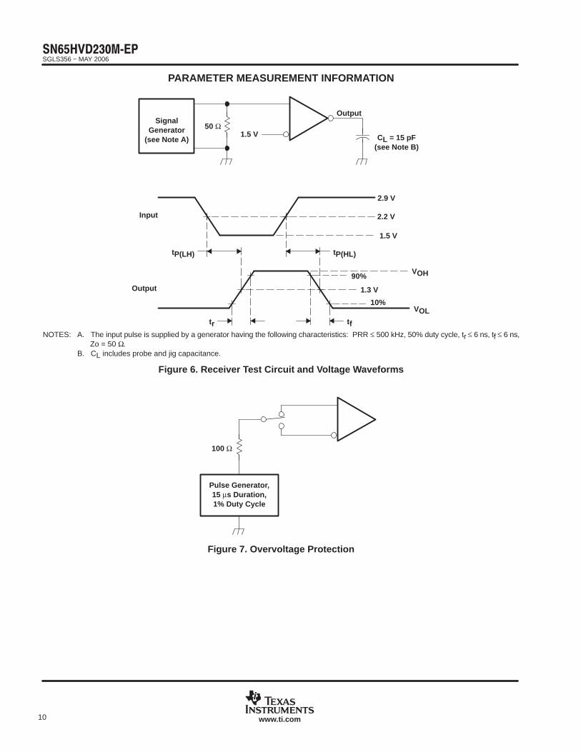
PARAMETER MEASUREMENT INFORMATION
50 ΩSignal
Generator(see Note A) CL = 15 pF
(see Note B)
1.5 V
90%
Output 1.3 V
10%
tf
VOL
VOH
tr
Input
1.5 V
2.9 V
tP(HL)
2.2 V
tP(LH)
Output
NOTES: A. The input pulse is supplied by a generator having the following characteristics: PRR ≤ 500 kHz, 50% duty cycle, tr ≤ 6 ns, tf ≤ 6 ns,Zo = 50 Ω.
B. CL includes probe and jig capacitance.
Figure 6. Receiver Test Circuit and Voltage Waveforms
100 Ω
Pulse Generator,15 µs Duration,1% Duty Cycle
Figure 7. Overvoltage Protection
SGLS356 − MAY 2006
11www.ti.com
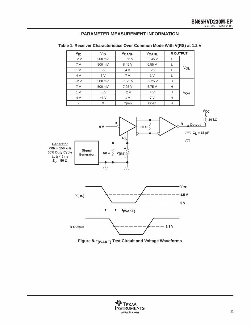
PARAMETER MEASUREMENT INFORMATION
Table 1. Receiver Characteristics Over Common Mode With V(RS) at 1.2 V
VIC VID VCANH VCANL R OUTPUT
−2 V 900 mV −1.55 V −2.45 V L
7 V 900 mV 8.45 V 6.55 V LVOL1 V 6 V 4 V −2 V LVOL
4 V 6 V 7 V 1 V L
−2 V 500 mV −1.75 V −2.25 V H
7 V 500 mV 7.25 V 6.75 V H
1 V −6 V −2 V 4 V H VOH4 V −6 V 1 V 7 V H
VOH
X X Open Open H
10 kΩ
0 V
CL = 15 pF
R Output 1.3 V
t(WAKE)
V(RS) 1.5 V
50 ΩSignal
Generator
GeneratorPRR = 150 kHz50% Duty Cycle
tr, tf < 6 nsZo = 50 Ω
V(RS)
D
RS
R Output
VCC
0 V
VCC
60 Ω
+
−
Figure 8. t (WAKE) Test Circuit and Voltage Waveforms

SGLS356 − MAY 2006
12 www.ti.com
TYPICAL CHARACTERISTICS
Figure 9
25
26
27
28
29
30
31
32
33
0 250 500 750 1000 1250 1500 1750 2000
− S
uppl
y C
urre
nt (
RM
S)
− m
A
SUPPLY CURRENT (RMS)vs
FREQUENCY
I CC
f − Frequency − kbps
Figure 10
−16
−14
−12
−10
−8
−6
−4
−2
0
0 0.6 1.1 1.6 2.1 2.6 3.1 3.6
LOGIC INPUT CURRENT (D PIN)vs
INPUT VOLTAGE
I I(L
)−
Logi
c In
put C
urre
nt −
Aµ
VI − Input Voltage − V
Figure 11
−400
−300
−200
−100
0
100
200
300
400
−7 −6 −4 −3 −1 0 1 3 4 6 7 8 10 11 12
VCC = 0 V
VCC = 3.6 V
BUS INPUT CURRENTvs
BUS INPUT VOLTAGE
I I−
Bus
Inpu
t Cur
rent
−A
µ
VI − Bus Input Voltage − V
Figure 12
0
20
40
60
80
100
120
140
160
180
0 1 2 3 4
DRIVER LOW-LEVEL OUTPUT CURRENTvs
LOW-LEVEL OUTPUT VOLTAGE
I OL
− D
river
Low
-Lev
el O
utpu
t Cur
rent
− m
A
VO(CANL)− Low-Level Output Voltage − V

SGLS356 − MAY 2006
13www.ti.com
TYPICAL CHARACTERISTICS
Figure 13
0
20
40
60
80
100
120
0 0.5 1 1.5 2 2.5 3 3.5
− D
river
Hig
h-Le
vel O
utpu
t Cur
rent
− m
A
DRIVER HIGH-LEVEL OUTPUT CURRENTvs
HIGH-LEVEL OUTPUT VOLTAGE
VO(CANH) − High-Level Output Voltage − V
IO
H
Figure 14
0
0.5
1
1.5
2
2.5
3
−55 −40 0 25 70 85 125
VCC = 3.6 V
VCC = 3.3 V
VCC = 3 V
DOMINANT VOLTAGE (V OD)vs
FREE-AIR TEMPERATURE
VO
D − D
omin
ant V
olta
ge −
V
TA − Free-Air Temperature − °C
Figure 15
30
31
32
33
34
35
36
37
38
−55 −40 0 25 70 85 125
VCC = 3.3 V
VCC = 3 V
VCC = 3.6 V
RECEIVER LOW-TO-HIGH PROPAGATION DELAY TIMEvs
FREE-AIR TEMPERATURE
RS = 0
t PLH
− R
ecei
ver
Low
-to-
Hig
h P
ropa
gatio
n D
elay
Tim
e −
ns
TA − Free-Air Temperature − °C
Figure 16
VCC = 3.3 V
VCC = 3 V
VCC = 3.6 V
34
35
36
37
38
39
40
−55 −40 0 25 70 85 125
RS = 0
RECEIVER HIGH-TO-LOW PROPAGATION DELAY TIMEvs
FREE-AIR TEMPERATURE
t PH
L−
Rec
eive
r H
igh-
to-L
ow P
ropa
gatio
n D
elay
Tim
e −
ns
TA − Free-Air Temperature − °C

SGLS356 − MAY 2006
14 www.ti.com
TYPICAL CHARACTERISTICS
Figure 17
10
15
20
25
30
35
40
45
50
55
−55 −40 0 25 70 85 125
VCC = 3.3 V
VCC = 3 V
VCC = 3.6 V
RS = 0
DRIVER LOW-TO-HIGH PROPAGATION DELAY TIMEvs
FREE-AIR TEMPERATURE
t PLH
− D
river
Low
-to-
Hig
h P
ropa
gatio
n D
elay
Tim
e −
ns
TA − Free-Air Temperature − °C
Figure 18
50
55
60
65
70
75
80
85
90
−55 −40 0 25 70 85 125
VCC = 3.3 V
VCC = 3 V
VCC = 3.6 VRS = 0
DRIVER HIGH-TO-LOW PROPAGATION DELAY TIMEvs
FREE-AIR TEMPERATURE
t PH
L−
Driv
er H
igh-
to-L
ow P
ropa
gatio
n D
elay
Tim
e −
ns
TA − Free-Air Temperature − °C
Figure 19
0
10
20
30
40
50
60
70
80
90
−55 −40 0 25 70 85 125
VCC = 3.3 V
VCC = 3 V
VCC = 3.6 V
RS = 10 kΩ
DRIVER LOW-TO-HIGH PROPAGATION DELAY TIMEvs
FREE-AIR TEMPERATURE
t PLH
− D
river
Low
-to-
Hig
h P
ropa
gatio
n D
elay
Tim
e −
ns
TA − Free-Air Temperature − °C
Figure 20
80
90
100
110
120
130
140
150
−55 −40 0 25 70 85 125
VCC = 3.3 V
VCC = 3 V
VCC = 3.6 VRS = 10 kΩ
DRIVER HIGH-TO-LOW PROPAGATION DELAY TIMEvs
FREE-AIR TEMPERATURE
t PH
L−
Driv
er H
igh-
to-L
ow P
ropa
gatio
n D
elay
Tim
e −
ns
TA − Free-Air Temperature − °C

SGLS356 − MAY 2006
15www.ti.com
TYPICAL CHARACTERISTICS
Figure 21
0
100
200
300
400
500
600
700
800
−55 −40 0 25 70 85 125
VCC = 3.3 V
VCC = 3 V
VCC = 3.6 V
RS = 100 kΩ
DRIVER LOW-TO-HIGH PROPAGATION DELAY TIMEvs
FREE-AIR TEMPERATURE
t PLH
− D
river
Low
-to-
Hig
h P
ropa
gatio
n D
elay
Tim
e −
ns
TA − Free-Air Temperature − °C
Figure 22
700
750
800
850
900
950
1000
−55 −40 0 25 70 85 125
VCC = 3.3 V
VCC = 3 V
VCC = 3.6 V
RS = 100 kΩ
DRIVER HIGH-TO-LOW PROPAGATION DELAY TIMEvs
FREE-AIR TEMPERATURE
t PH
L−
Driv
er H
igh-
to-L
ow P
ropa
gatio
n D
elay
Tim
e −
ns
TA − Free-Air Temperature − °C
Figure 23
−10
0
10
20
30
40
50
1 1.5 2 2.5 3 3.5 4
DRIVER OUTPUT CURRENTvs
SUPPLY VOLTAGE
I O−
Driv
er O
utpu
t Cur
rent
− m
A
VCC − Supply Voltage − V
Figure 24
0
0.10
0.20
0.30
0.40
0.50
0.60
0.70
0.80
0.90
1.00
1.10
1.20
1.30
1.40
0 50 100 150 200
1.50
VCC = 3.3 V
VCC = 3 V
VCC = 3.6 V
DIFFERENTIAL DRIVER OUTPUT FALL TIMEvs Source Resistance (R S)
t f−
Diff
eren
tial O
utpu
t Fal
l Tim
e −
sµ
Rs − Source Resistance − k Ω
SGLS356 − MAY 2006
16 www.ti.com
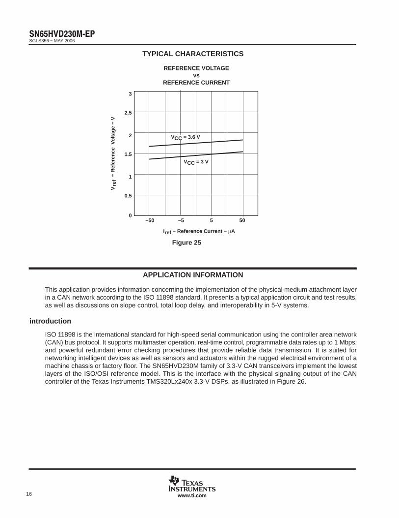
TYPICAL CHARACTERISTICS
Figure 25
0
0.5
1
1.5
2
2.5
3
−50 −5 5 50
VCC = 3 V
REFERENCE VOLTAGEvs
REFERENCE CURRENT
Vre
f−
Ref
eren
ce V
olta
ge −
V
Iref − Reference Current − µA
VCC = 3.6 V
APPLICATION INFORMATION
This application provides information concerning the implementation of the physical medium attachment layerin a CAN network according to the ISO 11898 standard. It presents a typical application circuit and test results,as well as discussions on slope control, total loop delay, and interoperability in 5-V systems.
introduction
ISO 11898 is the international standard for high-speed serial communication using the controller area network(CAN) bus protocol. It supports multimaster operation, real-time control, programmable data rates up to 1 Mbps,and powerful redundant error checking procedures that provide reliable data transmission. It is suited fornetworking intelligent devices as well as sensors and actuators within the rugged electrical environment of amachine chassis or factory floor. The SN65HVD230M family of 3.3-V CAN transceivers implement the lowestlayers of the ISO/OSI reference model. This is the interface with the physical signaling output of the CANcontroller of the Texas Instruments TMS320Lx240x 3.3-V DSPs, as illustrated in Figure 26.

SGLS356 − MAY 2006
17www.ti.com
APPLICATION INFORMATION
TMS320Lx2403/6/73.3-VDSP
ImplementationISO 11898 Specification
Application Specific Layer
Data-LinkLayer
Logic Link Control
Medium Access Control
PhysicalLayer
Physical Signaling
Physical Medium Attachment
Medium Dependant Interface
Embedded
CAN
Controller
SN65HVD230
CAN Bus−Line
Figure 26. The Layered ISO 11898 Standard Architecture
The SN65HVD230M family of CAN transceivers are compatible with the ISO 11898 standard; this ensuresinteroperability with other standard-compliant products.
application of the SN65HVD230M
Figure 27 illustrates a typical application of the SN65HVD230M family. The output of a DSP’s CAN controlleris connected to the serial driver input, pin D, and receiver serial output, pin R, of the transceiver. The transceiveris then attached to the differential bus lines at pins CANH and CANL. Typically, the bus is a twisted pair of wireswith a characteristic impedance of 120 Ω, in the standard half-duplex multipoint topology of Figure 28. Each endof the bus is terminated with 120-Ω resistors in compliance with the standard to minimize signal reflections onthe bus.
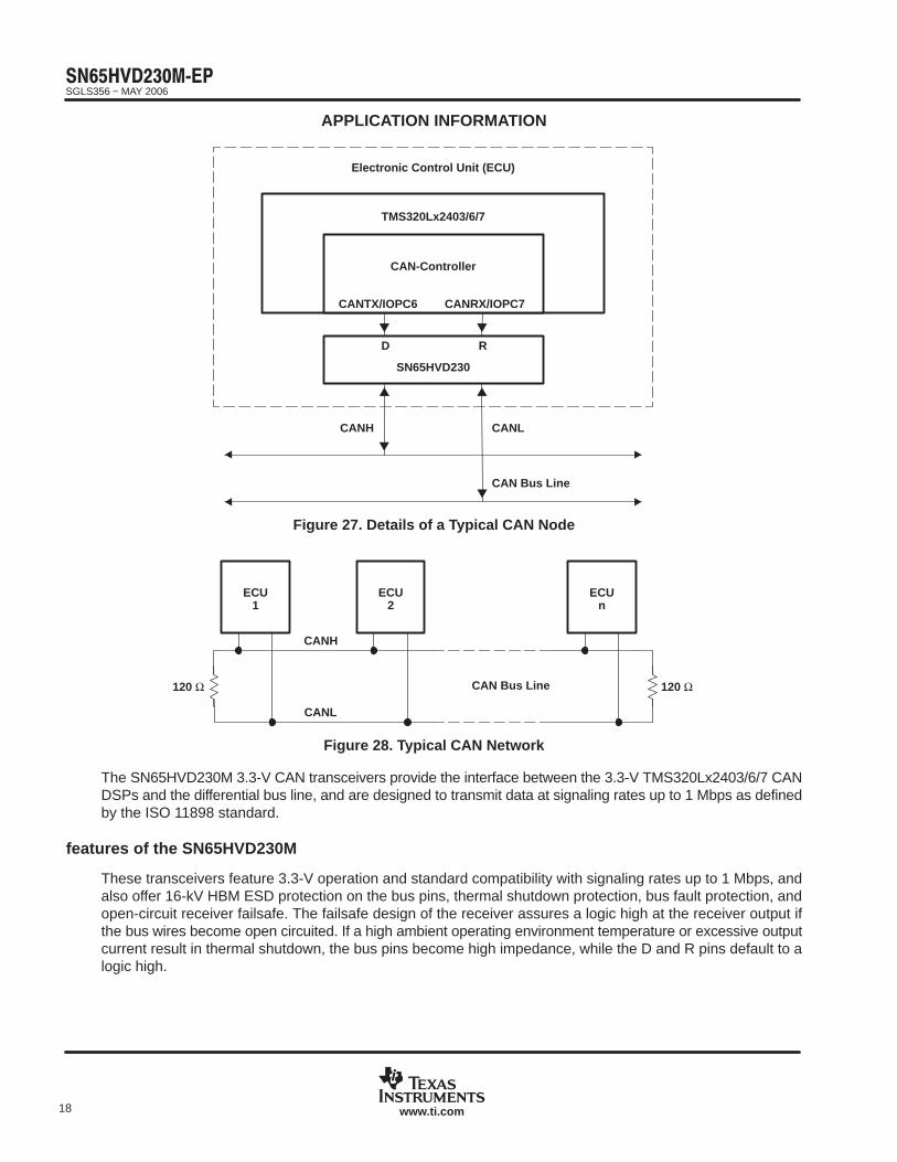
SGLS356 − MAY 2006
18 www.ti.com
APPLICATION INFORMATION
TMS320Lx2403/6/7
CAN Bus Line
CAN-Controller
CANTX/IOPC6
SN65HVD230
Electronic Control Unit (ECU)
CANH CANL
D R
CANRX/IOPC7
Figure 27. Details of a Typical CAN Node
CANH
CANL
CAN Bus Line
ECU ECU ECU1 2 n
120 Ω120 Ω
Figure 28. Typical CAN Network
The SN65HVD230M 3.3-V CAN transceivers provide the interface between the 3.3-V TMS320Lx2403/6/7 CANDSPs and the differential bus line, and are designed to transmit data at signaling rates up to 1 Mbps as definedby the ISO 11898 standard.
features of the SN65HVD230M
These transceivers feature 3.3-V operation and standard compatibility with signaling rates up to 1 Mbps, andalso offer 16-kV HBM ESD protection on the bus pins, thermal shutdown protection, bus fault protection, andopen-circuit receiver failsafe. The failsafe design of the receiver assures a logic high at the receiver output ifthe bus wires become open circuited. If a high ambient operating environment temperature or excessive outputcurrent result in thermal shutdown, the bus pins become high impedance, while the D and R pins default to alogic high.

SGLS356 − MAY 2006
19www.ti.com
APPLICATION INFORMATION
features of the SN65HVD230M (continued)
The bus pins are also maintained in a high-impedance state during low VCC conditions to ensure glitch-freepower-up and power-down bus protection for hot-plugging applications. This high-impedance condition alsomeans that an unpowered node will not disturb the bus. Transceivers without this feature usually have a lowoutput impedance. This results in a high current demand when the transceiver is unpowered, a condition thatcould affect the entire bus.
operating modes
RS (pin 8) of the SN65HVD230M provides for three different modes of operation: high-speed mode,slope-control mode, and low-power standby mode.
high-speed mode
The high-speed mode can be selected by applying a logic low to Rs (pin 8). The high-speed mode of operationis commonly employed in industrial applications. High-speed allows the output to switch as fast as possible withno internal limitation on the output rise and fall slopes. The only limitations of the high-speed operation are cablelength and radiated emission concerns, each of which is addressed by the slope control mode of operation.
If the low-power standby mode is to be employed in the circuit, direct connection to a DSP output pin can beused to switch between a logic-low level (< 1 V) for high speed mode operation, and the logic-high level (> 0.75VCC) for standby mode operation. Figure 29 shows a typical DSP connection and Figure 30 shows theSN65HVD230M driver output signal in high-speed mode on the CAN bus.
TMS320LF2406or
TMS320LF2407
IOPF61
2
3
4
8
7
6
5
DGNDVCC
R
CANHCANLVref
RS
SN65HVD230M
Figure 29. R S (Pin 8) Connection to a TMS320LF2406/07 for High-Speed or Standby Mode Operation

SGLS356 − MAY 2006
20 www.ti.com
APPLICATION INFORMATION
high-speed mode (continued)
1
1 MbpsDriver Output
NRZ Data
Figure 30. Typical SN65HVD230M High-Speed Mode Output Waveform Into a 60- Ω Load
slope-control mode
Electromagnetic compatibility is essential in many applications using unshielded bus cable to reduce systemcost. To reduce the electromagnetic interference generated by fast rise times and resulting harmonics, the riseand fall slopes of the SN65HVD230M driver outputs can be adjusted by connecting a resistor from RS (pin 8)to ground or to a logic low voltage, as shown in Figure 31. The slope of the driver output signal is proportionalto the pin’s output current. This slope control is implemented with an external resistor value of 10 kΩ to achievea ≈ 15 V/µs slew rate, and up to 100 kΩ to achieve a ≈ 2 V/µs slew rate as displayed in Figure 32. Typical driveroutput waveforms from a pulse input signal with and without slope control are displayed in Figure 33. A pulseinput is used rather than NRZ data to clearly display the actual slew rate.
TMS320LF2406or
TMS320LF2407
IOPF61
2
3
4
8
7
6
5
DGNDVCC
R
CANHCANLVref
10 kΩto
100 kΩRS
SN65HVD230M
Figure 31. Slope-Control or Standby Mode Connection to a DSP

SGLS356 − MAY 2006
21www.ti.com
APPLICATION INFORMATION
Slope Control Resistance − k Ω
0
5
10
15
20
25
0 10 20 30 40 50 60 70 80 90
Driv
er O
utpu
t Sig
nal S
lope
− V
/µs
DRIVER OUTPUT SIGNAL SLOPEvs
SLOPE CONTROL RESISTANCE
4.70 6.8 10 15 22 33 47 68 100
Figure 32. SN65HVD230M Driver Output Signal Slope vs Slope Control Resistance Value
RS = 0 Ω
RS = 10 kΩ
RS = 100 kΩ
Figure 33. Typical SN65HVD230M 250-kbps Output Pulse Waveforms With Slope Control

SGLS356 − MAY 2006
22 www.ti.com
APPLICATION INFORMATION
standby mode (listen only mode) of the SN65HVD230M
If a logic high (> 0.75 VCC) is applied to RS (pin 8) in Figure 29 and Figure 31, the circuit of the SN65HVD230Menters a low-current, listen only standby mode during which the driver is switched off and the receiver remainsactive. In this listen only state, the transceiver is completely passive to the bus. It makes no difference if a slopecontrol resistor is in place as shown in Figure 31. The DSP can reverse this low-power standby mode when therising edge of a dominant state (bus differential voltage > 900 mV typical) occurs on the bus. The DSP, sensingbus activity, reactivates the driver circuit by placing a logic low (< 1.2 V) on RS (pin 8).
loop propagation delay
Transceiver loop delay is a measure of the overall device propagation delay, consisting of the delay from thedriver input to the differential outputs, plus the delay from the receiver inputs to its output.
The loop delay of the transceiver displayed in Figure 34 increases accordingly when slope control is being used.This increased loop delay means that the total bus length must be reduced to meet the CAN bit-timingrequirements of the overall system. The loop delay becomes ≈100 ns when employing slope control with a10-kΩ resistor, and ≈500 ns with a 100-kΩ resistor. Therefore, considering that the rule-of-thumb propagationdelay of typical bus cable is 5 ns/m, slope control with the 100-kΩ resistor decreases the allowable bus lengthby the difference between the 500-ns max loop delay and the loop delay with no slope control, 70.7 ns. Thisequates to (500–70.7 ns)/5 ns, or approximately 86 m less bus length. This slew-rate/bus length trade-off toreduce electromagnetic interference to adjoining circuits from the bus can also be solved with a high-qualityshielded bus cable.

SGLS356 − MAY 2006
23www.ti.com
APPLICATION INFORMATION
Figure 34. 70.7-ns Loop Delay Through the SN65HVD230M With R S = 0

SGLS356 − MAY 2006
24 www.ti.com
APPLICATION INFORMATION
interoperability with 5-V CAN systems
It is essential that the 3.3-V SN65HVD230M family performs seamlessly with 5-V transceivers because of thelarge number of 5-V devices installed. Figure 35 displays a test bus of a 3.3-V node with the SN65HVD230M,and three 5-V nodes: one for each of TI’s SN65LBC031 and UC5350 transceivers, and one using a competitorX250 transceiver.
SN65HVD230Q
TektronixHFS−9003
PatternGenerator
Tektronix784D
OscilloscopeTriggerInput
One Meter Belden Cable #82841
Competitor X250SN65LBC031 UC5350
HP E3516A3.3-V Power
Supply
HP E3516A5-V Power
Supply
TektronixP6243
Single-EndedProbes
120 Ω120 Ω
Figure 35. 3.3-V/5-V CAN Transceiver Test Bed

SGLS356 − MAY 2006
25www.ti.com
APPLICATION INFORMATION
DriverInput
CANBus
ReceiverOutput
Figure 36. SN65HVD230M’s Input, CAN Bus, and X250’s RXD Output Waveforms
Figure 36 displays the SN65HVD230M’s input signal, the CAN bus, and the competitor X250’s receiver outputwaveforms. The input waveform from the Tektronix HFS-9003 Pattern Generator in Figure 35 to theSN65HVD230M is a 250-kbps pulse for this test. The circuit is monitored with Tektronix P6243, 1-GHzsingle-ended probes in order to display the CAN dominant and recessive bus states.
Figure 36 displays the 250-kbps pulse input waveform to the SN65HVD230M on channel 1. Channels 2 and3 display CANH and CANL respectively, with their recessive bus states overlaying each other to clearly displaythe dominant and recessive CAN bus states. Channel 4 is the receiver output waveform of the competitor X250.

PACKAGE OPTION ADDENDUM
www.ti.com 31-May-2014
Addendum-Page 1
PACKAGING INFORMATION
Orderable Device Status(1)
Package Type PackageDrawing
Pins PackageQty
Eco Plan(2)
Lead/Ball Finish(6)
MSL Peak Temp(3)
Op Temp (°C) Device Marking(4/5)
Samples
SN65HVD230MDREP ACTIVE SOIC D 8 2500 Green (RoHS& no Sb/Br)
CU NIPDAU Level-1-260C-UNLIM -55 to 125 H230EP
V62/06629-01XE ACTIVE SOIC D 8 2500 Green (RoHS& no Sb/Br)
CU NIPDAU Level-1-260C-UNLIM -55 to 125 H230EP
(1) The marketing status values are defined as follows:ACTIVE: Product device recommended for new designs.LIFEBUY: TI has announced that the device will be discontinued, and a lifetime-buy period is in effect.NRND: Not recommended for new designs. Device is in production to support existing customers, but TI does not recommend using this part in a new design.PREVIEW: Device has been announced but is not in production. Samples may or may not be available.OBSOLETE: TI has discontinued the production of the device.
(2) Eco Plan - The planned eco-friendly classification: Pb-Free (RoHS), Pb-Free (RoHS Exempt), or Green (RoHS & no Sb/Br) - please check http://www.ti.com/productcontent for the latest availabilityinformation and additional product content details.TBD: The Pb-Free/Green conversion plan has not been defined.Pb-Free (RoHS): TI's terms "Lead-Free" or "Pb-Free" mean semiconductor products that are compatible with the current RoHS requirements for all 6 substances, including the requirement thatlead not exceed 0.1% by weight in homogeneous materials. Where designed to be soldered at high temperatures, TI Pb-Free products are suitable for use in specified lead-free processes.Pb-Free (RoHS Exempt): This component has a RoHS exemption for either 1) lead-based flip-chip solder bumps used between the die and package, or 2) lead-based die adhesive used betweenthe die and leadframe. The component is otherwise considered Pb-Free (RoHS compatible) as defined above.Green (RoHS & no Sb/Br): TI defines "Green" to mean Pb-Free (RoHS compatible), and free of Bromine (Br) and Antimony (Sb) based flame retardants (Br or Sb do not exceed 0.1% by weightin homogeneous material)
(3) MSL, Peak Temp. - The Moisture Sensitivity Level rating according to the JEDEC industry standard classifications, and peak solder temperature.
(4) There may be additional marking, which relates to the logo, the lot trace code information, or the environmental category on the device.
(5) Multiple Device Markings will be inside parentheses. Only one Device Marking contained in parentheses and separated by a "~" will appear on a device. If a line is indented then it is a continuationof the previous line and the two combined represent the entire Device Marking for that device.
(6) Lead/Ball Finish - Orderable Devices may have multiple material finish options. Finish options are separated by a vertical ruled line. Lead/Ball Finish values may wrap to two lines if the finishvalue exceeds the maximum column width.
Important Information and Disclaimer:The information provided on this page represents TI's knowledge and belief as of the date that it is provided. TI bases its knowledge and belief on informationprovided by third parties, and makes no representation or warranty as to the accuracy of such information. Efforts are underway to better integrate information from third parties. TI has taken andcontinues to take reasonable steps to provide representative and accurate information but may not have conducted destructive testing or chemical analysis on incoming materials and chemicals.TI and TI suppliers consider certain information to be proprietary, and thus CAS numbers and other limited information may not be available for release.

PACKAGE OPTION ADDENDUM
www.ti.com 31-May-2014
Addendum-Page 2
In no event shall TI's liability arising out of such information exceed the total purchase price of the TI part(s) at issue in this document sold by TI to Customer on an annual basis.

TAPE AND REEL INFORMATION
*All dimensions are nominal
Device PackageType
PackageDrawing
Pins SPQ ReelDiameter
(mm)
ReelWidth
W1 (mm)
A0(mm)
B0(mm)
K0(mm)
P1(mm)
W(mm)
Pin1Quadrant
SN65HVD230MDREP SOIC D 8 2500 330.0 12.4 6.4 5.2 2.1 8.0 12.0 Q1
PACKAGE MATERIALS INFORMATION
www.ti.com 26-Jan-2013
Pack Materials-Page 1
*All dimensions are nominal
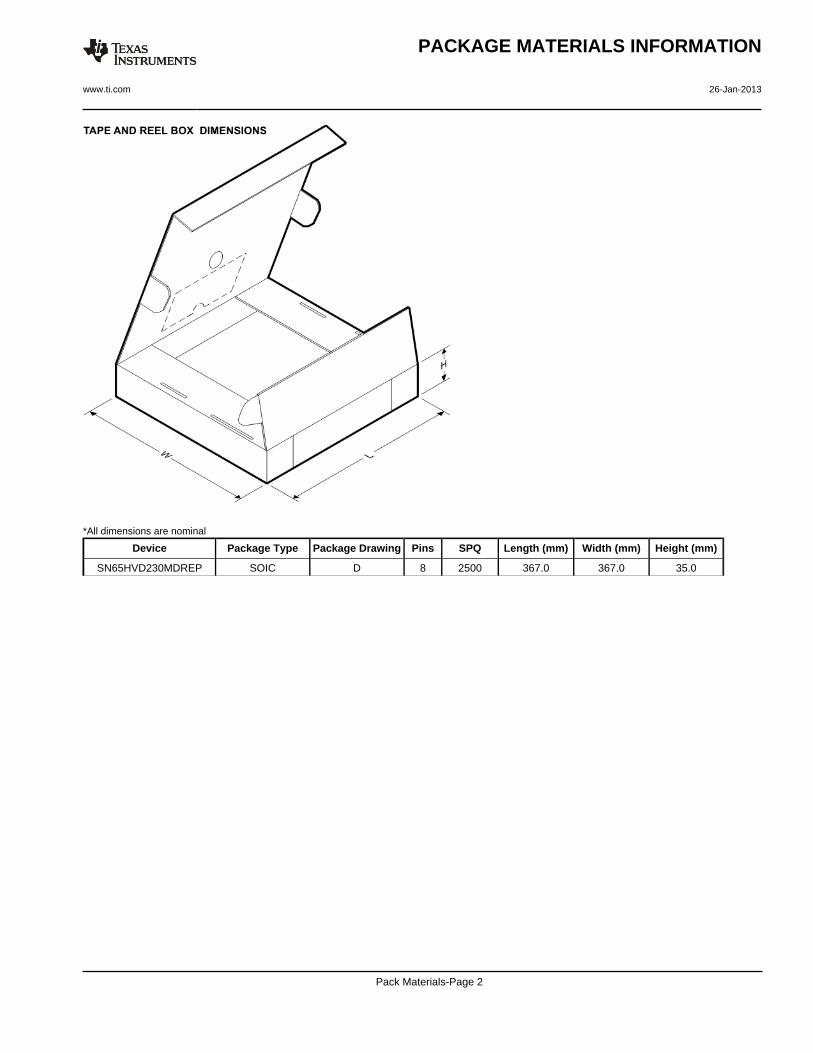
Device Package Type Package Drawing Pins SPQ Length (mm) Width (mm) Height (mm)
SN65HVD230MDREP SOIC D 8 2500 367.0 367.0 35.0
PACKAGE MATERIALS INFORMATION
www.ti.com 26-Jan-2013
Pack Materials-Page 2


IMPORTANT NOTICETexas Instruments Incorporated and its subsidiaries (TI) reserve the right to make corrections, enhancements, improvements and otherchanges to its semiconductor products and services per JESD46, latest issue, and to discontinue any product or service per JESD48, latestissue. Buyers should obtain the latest relevant information before placing orders and should verify that such information is current andcomplete. All semiconductor products (also referred to herein as “components”) are sold subject to TI’s terms and conditions of salesupplied at the time of order acknowledgment.TI warrants performance of its components to the specifications applicable at the time of sale, in accordance with the warranty in TI’s termsand conditions of sale of semiconductor products. Testing and other quality control techniques are used to the extent TI deems necessaryto support this warranty. Except where mandated by applicable law, testing of all parameters of each component is not necessarilyperformed.TI assumes no liability for applications assistance or the design of Buyers’ products. Buyers are responsible for their products andapplications using TI components. To minimize the risks associated with Buyers’ products and applications, Buyers should provideadequate design and operating safeguards.TI does not warrant or represent that any license, either express or implied, is granted under any patent right, copyright, mask work right, orother intellectual property right relating to any combination, machine, or process in which TI components or services are used. Informationpublished by TI regarding third-party products or services does not constitute a license to use such products or services or a warranty orendorsement thereof. Use of such information may require a license from a third party under the patents or other intellectual property of thethird party, or a license from TI under the patents or other intellectual property of TI.Reproduction of significant portions of TI information in TI data books or data sheets is permissible only if reproduction is without alterationand is accompanied by all associated warranties, conditions, limitations, and notices. TI is not responsible or liable for such altereddocumentation. Information of third parties may be subject to additional restrictions.Resale of TI components or services with statements different from or beyond the parameters stated by TI for that component or servicevoids all express and any implied warranties for the associated TI component or service and is an unfair and deceptive business practice.TI is not responsible or liable for any such statements.Buyer acknowledges and agrees that it is solely responsible for compliance with all legal, regulatory and safety-related requirementsconcerning its products, and any use of TI components in its applications, notwithstanding any applications-related information or supportthat may be provided by TI. Buyer represents and agrees that it has all the necessary expertise to create and implement safeguards whichanticipate dangerous consequences of failures, monitor failures and their consequences, lessen the likelihood of failures that might causeharm and take appropriate remedial actions. Buyer will fully indemnify TI and its representatives against any damages arising out of the useof any TI components in safety-critical applications.In some cases, TI components may be promoted specifically to facilitate safety-related applications. With such components, TI’s goal is tohelp enable customers to design and create their own end-product solutions that meet applicable functional safety standards andrequirements. Nonetheless, such components are subject to these terms.No TI components are authorized for use in FDA Class III (or similar life-critical medical equipment) unless authorized officers of the partieshave executed a special agreement specifically governing such use.Only those TI components which TI has specifically designated as military grade or “enhanced plastic” are designed and intended for use inmilitary/aerospace applications or environments. Buyer acknowledges and agrees that any military or aerospace use of TI componentswhich have not been so designated is solely at the Buyer's risk, and that Buyer is solely responsible for compliance with all legal andregulatory requirements in connection with such use.TI has specifically designated certain components as meeting ISO/TS16949 requirements, mainly for automotive use. In any case of use ofnon-designated products, TI will not be responsible for any failure to meet ISO/TS16949.Products ApplicationsAudio www.ti.com/audio Automotive and Transportation www.ti.com/automotiveAmplifiers amplifier.ti.com Communications and Telecom www.ti.com/communicationsData Converters dataconverter.ti.com Computers and Peripherals www.ti.com/computersDLP® Products www.dlp.com Consumer Electronics www.ti.com/consumer-appsDSP dsp.ti.com Energy and Lighting www.ti.com/energyClocks and Timers www.ti.com/clocks Industrial www.ti.com/industrialInterface interface.ti.com Medical www.ti.com/medicalLogic logic.ti.com Security www.ti.com/securityPower Mgmt power.ti.com Space, Avionics and Defense www.ti.com/space-avionics-defenseMicrocontrollers microcontroller.ti.com Video and Imaging www.ti.com/videoRFID www.ti-rfid.comOMAP Applications Processors www.ti.com/omap TI E2E Community e2e.ti.comWireless Connectivity www.ti.com/wirelessconnectivity
Mailing Address: Texas Instruments, Post Office Box 655303, Dallas, Texas 75265Copyright © 2014, Texas Instruments Incorporated