smpte uhd-sdi receiver subsystem v2 - xilinx · the smpte uhd-sdi rx subsystem is provided at no...
TRANSCRIPT

SMPTE UHD-SDI Receiver Subsystem v2.0
Product Guide
Vivado Design SuitePG290 November 08, 2019

SMPTE UHD-SDI RX Subsystem v2.0 2PG290 November 08, 2019 www.xilinx.com
Table of ContentsIP Facts
Chapter 1: OverviewIntroduction . . . . . . . . . . . . . . . . . . . . . . . . . . . . . . . . . . . . . . . . . . . . . . . . . . . . . . . . . . . . . . . . . . . . . . 5Subcore Details . . . . . . . . . . . . . . . . . . . . . . . . . . . . . . . . . . . . . . . . . . . . . . . . . . . . . . . . . . . . . . . . . . . 6Applications . . . . . . . . . . . . . . . . . . . . . . . . . . . . . . . . . . . . . . . . . . . . . . . . . . . . . . . . . . . . . . . . . . . . . . 7Unsupported Features. . . . . . . . . . . . . . . . . . . . . . . . . . . . . . . . . . . . . . . . . . . . . . . . . . . . . . . . . . . . . . 7Licensing . . . . . . . . . . . . . . . . . . . . . . . . . . . . . . . . . . . . . . . . . . . . . . . . . . . . . . . . . . . . . . . . . . . . . . . . . 7
Chapter 2: Product SpecificationStandards . . . . . . . . . . . . . . . . . . . . . . . . . . . . . . . . . . . . . . . . . . . . . . . . . . . . . . . . . . . . . . . . . . . . . . . . 8Performance. . . . . . . . . . . . . . . . . . . . . . . . . . . . . . . . . . . . . . . . . . . . . . . . . . . . . . . . . . . . . . . . . . . . . . 8Resource Utilization. . . . . . . . . . . . . . . . . . . . . . . . . . . . . . . . . . . . . . . . . . . . . . . . . . . . . . . . . . . . . . . . 9Port Descriptions . . . . . . . . . . . . . . . . . . . . . . . . . . . . . . . . . . . . . . . . . . . . . . . . . . . . . . . . . . . . . . . . . . 9Register Space . . . . . . . . . . . . . . . . . . . . . . . . . . . . . . . . . . . . . . . . . . . . . . . . . . . . . . . . . . . . . . . . . . . 16
Chapter 3: Designing with the CoreGeneral Design Guidelines . . . . . . . . . . . . . . . . . . . . . . . . . . . . . . . . . . . . . . . . . . . . . . . . . . . . . . . . . 30Clocking. . . . . . . . . . . . . . . . . . . . . . . . . . . . . . . . . . . . . . . . . . . . . . . . . . . . . . . . . . . . . . . . . . . . . . . . . 31Resets . . . . . . . . . . . . . . . . . . . . . . . . . . . . . . . . . . . . . . . . . . . . . . . . . . . . . . . . . . . . . . . . . . . . . . . . . . 32UHD-SDI Audio Extract Use Case . . . . . . . . . . . . . . . . . . . . . . . . . . . . . . . . . . . . . . . . . . . . . . . . . . . . 33
Chapter 4: Design Flow StepsCustomizing and Generating the Core . . . . . . . . . . . . . . . . . . . . . . . . . . . . . . . . . . . . . . . . . . . . . . . . 36Core Configuration Tab . . . . . . . . . . . . . . . . . . . . . . . . . . . . . . . . . . . . . . . . . . . . . . . . . . . . . . . . . . . . 37Application Example Design Tab. . . . . . . . . . . . . . . . . . . . . . . . . . . . . . . . . . . . . . . . . . . . . . . . . . . . . 38Constraining the Core . . . . . . . . . . . . . . . . . . . . . . . . . . . . . . . . . . . . . . . . . . . . . . . . . . . . . . . . . . . . . 39Simulation . . . . . . . . . . . . . . . . . . . . . . . . . . . . . . . . . . . . . . . . . . . . . . . . . . . . . . . . . . . . . . . . . . . . . . 41Synthesis and Implementation . . . . . . . . . . . . . . . . . . . . . . . . . . . . . . . . . . . . . . . . . . . . . . . . . . . . . . 41
Chapter 5: Example DesignZCU106 SMPTE UHD-SDI RX-Only Example Design . . . . . . . . . . . . . . . . . . . . . . . . . . . . . . . . . . . . . . 43ZCU106 SMPTE UHD-SDI Pass-Through Example Design. . . . . . . . . . . . . . . . . . . . . . . . . . . . . . . . . . 52ZCU106 SMPTE UHD-SDI Audio-Video Pass-Through Example Design. . . . . . . . . . . . . . . . . . . . . . . 65
Send Feedback

SMPTE UHD-SDI RX Subsystem v2.0 3PG290 November 08, 2019 www.xilinx.com
KCU116 SMPTE UHD-SDI Audio-Video Loopback Example Design . . . . . . . . . . . . . . . . . . . . . . . . . . 76
Appendix A: Verification, Compliance, and InteroperabilityInteroperability . . . . . . . . . . . . . . . . . . . . . . . . . . . . . . . . . . . . . . . . . . . . . . . . . . . . . . . . . . . . . . . . . . 87Hardware Validation . . . . . . . . . . . . . . . . . . . . . . . . . . . . . . . . . . . . . . . . . . . . . . . . . . . . . . . . . . . . . . 88Video Resolutions . . . . . . . . . . . . . . . . . . . . . . . . . . . . . . . . . . . . . . . . . . . . . . . . . . . . . . . . . . . . . . . . 89
Appendix B: DebuggingFinding Help on Xilinx.com . . . . . . . . . . . . . . . . . . . . . . . . . . . . . . . . . . . . . . . . . . . . . . . . . . . . . . . . . 98Debug Tools . . . . . . . . . . . . . . . . . . . . . . . . . . . . . . . . . . . . . . . . . . . . . . . . . . . . . . . . . . . . . . . . . . . . . 99Hardware Debug . . . . . . . . . . . . . . . . . . . . . . . . . . . . . . . . . . . . . . . . . . . . . . . . . . . . . . . . . . . . . . . . 100Interface Debug . . . . . . . . . . . . . . . . . . . . . . . . . . . . . . . . . . . . . . . . . . . . . . . . . . . . . . . . . . . . . . . . . 103
Appendix C: UHD-SDI GT 2.0 IPUsing UltraScale+ GTH/GTY Transceivers for SDI . . . . . . . . . . . . . . . . . . . . . . . . . . . . . . . . . . . . . . 105UHD-SDI GT Ports. . . . . . . . . . . . . . . . . . . . . . . . . . . . . . . . . . . . . . . . . . . . . . . . . . . . . . . . . . . . . . . . 112Clocking. . . . . . . . . . . . . . . . . . . . . . . . . . . . . . . . . . . . . . . . . . . . . . . . . . . . . . . . . . . . . . . . . . . . . . . . 121GT COMMON Shared Logic . . . . . . . . . . . . . . . . . . . . . . . . . . . . . . . . . . . . . . . . . . . . . . . . . . . . . . . . 122Customizing and Generating the Core . . . . . . . . . . . . . . . . . . . . . . . . . . . . . . . . . . . . . . . . . . . . . . . 123Constraining the Core . . . . . . . . . . . . . . . . . . . . . . . . . . . . . . . . . . . . . . . . . . . . . . . . . . . . . . . . . . . . 130I/O Planning . . . . . . . . . . . . . . . . . . . . . . . . . . . . . . . . . . . . . . . . . . . . . . . . . . . . . . . . . . . . . . . . . . . . 131
Appendix D: Audio Test Pattern Generator IPFeature Summary. . . . . . . . . . . . . . . . . . . . . . . . . . . . . . . . . . . . . . . . . . . . . . . . . . . . . . . . . . . . . . . . 132Unsupported Features, Limitations . . . . . . . . . . . . . . . . . . . . . . . . . . . . . . . . . . . . . . . . . . . . . . . . . 132Port Descriptions . . . . . . . . . . . . . . . . . . . . . . . . . . . . . . . . . . . . . . . . . . . . . . . . . . . . . . . . . . . . . . . . 133Register Space . . . . . . . . . . . . . . . . . . . . . . . . . . . . . . . . . . . . . . . . . . . . . . . . . . . . . . . . . . . . . . . . . . 133Clocking. . . . . . . . . . . . . . . . . . . . . . . . . . . . . . . . . . . . . . . . . . . . . . . . . . . . . . . . . . . . . . . . . . . . . . . . 138Resets . . . . . . . . . . . . . . . . . . . . . . . . . . . . . . . . . . . . . . . . . . . . . . . . . . . . . . . . . . . . . . . . . . . . . . . . . 138Programming Sequence. . . . . . . . . . . . . . . . . . . . . . . . . . . . . . . . . . . . . . . . . . . . . . . . . . . . . . . . . . . 139
Appendix E: Additional Resources and Legal NoticesXilinx Resources . . . . . . . . . . . . . . . . . . . . . . . . . . . . . . . . . . . . . . . . . . . . . . . . . . . . . . . . . . . . . . . . . 140Documentation Navigator and Design Hubs . . . . . . . . . . . . . . . . . . . . . . . . . . . . . . . . . . . . . . . . . . 140References . . . . . . . . . . . . . . . . . . . . . . . . . . . . . . . . . . . . . . . . . . . . . . . . . . . . . . . . . . . . . . . . . . . . . 141Revision History . . . . . . . . . . . . . . . . . . . . . . . . . . . . . . . . . . . . . . . . . . . . . . . . . . . . . . . . . . . . . . . . . 142Please Read: Important Legal Notices . . . . . . . . . . . . . . . . . . . . . . . . . . . . . . . . . . . . . . . . . . . . . . . 142
Send Feedback

SMPTE UHD-SDI RX Subsystem v2.0 4PG290 November 08, 2019 www.xilinx.com Product Specification
IntroductionThe Society of Motion Picture and Television Engineers (SMPTE) UHD-SDI receiver subsystem implements an SDI receive interface in accordance with the serial digital interface (SDI) family of standards. The subsystem receives video from a native SDI and generates AXI4-Stream video. The subsystem allows fast selection of the top level parameters and automates most of the lower level parameterization. The AXI4-Stream video interface allows a seamless interface to other AXI4-Stream-based subsystems.
Features• Supports AXI4-Stream, native video and
native SDI user interfaces• Support for 2 pixel per sample• 10-bit per color component• Supports YUV 4:4:4, YUV 4:2:2, and YUV 4:2:0
color space• AXI4-Lite interface for register access to
configure different subsystem options• Audio support• Standards compliance:
° SMPTE ST 259: SD-SDI at 270 Mb/s° SMPTE RP 165: EDH for SD-SDI° SMPTE ST 292: HD-SDI at 1.485 Gb/s and
1.485/1.001 Gb/s° SMPTE ST 372: Dual Link HD-SDI° SMPTE ST 424: 3G-SDI with data mapped
by any ST 425-x mapping at 2.97 Gb/s and 2.97/1.001 Gb/s
° SMPTE ST 2081-1: 6G-SDI with data mapped by any ST 2081-x mapping at 5.94 Gb/s and 5.94/1.001 Gb/s
° SMPTE ST 2082-1: 12G-SDI with data mapped by any ST 2082-x mapping at 11.88 Gb/s and 11.88/1.001 Gb/s
° Dual link and quad link 6G-SDI and 12G-SDI supported by instantiating two or four SMPTE UHD-SDI RX subsystems
° SMPTE ST 352: Payload ID packets fully supported
IP Facts
LogiCORE IP Facts TableCore Specifics
Supported Device Family(1)
UltraScale+™ Families (GTHE4, GTYE4)Zynq® UltraScale+ MPSoC (GTHE4, GTYE4)
Zynq UltraScale+ RFSoCSupported User Interfaces
AXI4-Lite, AXI4-Stream,native video, and native SDI
Resources Performance and Resource Utilization web pageProvided with Core
Design Files Hierarchical subsystem packaged withSMPTE UHD-SDI RX core and other IP cores
Example Design Vivado IP IntegratorTest Bench N/AConstraints File IP cores delivered with XDC filesSimulation Model N/A
SupportedS/W Driver(2) Standalone and Linux
Tested Design Flows(3)
Design Entry Vivado® Design Suite
Simulation For supported simulators, see theXilinx Design Tools: Release Notes Guide.
Synthesis Vivado SynthesisSupport
Release Notes and Known Issues
Master Answer Record: 68766
Provided by Xilinx @ www.xilinx.com/support
Notes: 1. For a complete list of supported devices, see the Vivado IP
catalog.2. Standalone driver details can be found in the Vitis directory
(<install_directory>/Vitis/<release>/data/embeddedsw/doc/xilinx_drivers.htm). Linux OS and driver support information is available from http://www.wiki.xilinx.com/Xilinx+V4L2+SDI+Rx+driver.
3. For the supported versions of the tools, see theXilinx Design Tools: Release Notes Guide.
Send Feedback

SMPTE UHD-SDI RX Subsystem v2.0 5PG290 November 08, 2019 www.xilinx.com
Chapter 1
Overview
IntroductionThe SMPTE UHD-SDI Receiver (RX) Subsystem allows you to quickly create systems based on SMPTE SDI protocols. It receives unaligned native SDI streams from the SDI GT PHY and outputs an AXI4-Stream video stream, native video, or native SDI using Xilinx® transceivers as the physical layer. The top-level customization parameters select the required hardware blocks required to build the subsystem. Figure 1-1 shows the subsystem architecture using the AXI4-Stream user interface.
Figure 1-2 shows the SMPTE UHD-SDI RX Subsystem with native video as the user interface. The SMPTE UHD-SDI (RX) IP core and SDI RX to Video Bridge IP core are present in the subsystem and the subsystem outputs native video.
X-Ref Target - Figure 1-1
Figure 1-1: SMPTE UHD-SDI RX Subsystem AXI4-Stream Architecture
X-Ref Target - Figure 1-2
Figure 1-2: SMPTE UHD-SDI RX Subsystem Native Video Architecture
Send Feedback

SMPTE UHD-SDI RX Subsystem v2.0 6PG290 November 08, 2019 www.xilinx.com
Chapter 1: Overview
Figure 1-3 shows the SMPTE UHD-SDI RX Subsystem with native SDI as the user interface. The subsystem accepts native SDI input and consists only of the SMPTE UHD-SDI (RX) IP core.
The subsystem consists of the following subcores:
• SMPTE UHD-SDI (RX) • SDI RX to Video Bridge• Video In to AXI4-Stream
Subcore DetailsSMTPE UHD-SDI (RX)The SMPTE UHD-SDI core receives multiplexed native SDI data streams and generates a non-multiplexed 10-bit SDI data stream. See the LogiCORE IP SMPTE UHD-SDI Product Guide (PG205) [Ref 9] for details.
SDI RX to Video BridgeThe SDI RX to Video Bridge LogiCORE IP core is designed to interface between native SDI and native video. The input is an SDI virtual interface that has one to eight 10-bit data streams with embedded synchronization. The output is video data with explicit synchronization signals. This core extracts synchronization signals, reformats the video data, and provides clock enables.
The core extracts embedded synchronization signals from the SDI data stream. It supports SD-SDI, HD-SDI, 3G-SDI Level A, 3G-SDI Level B, 6G-SDI and 12G-SDI with Y, Cb, Cr data format at 10 bits per component. For 3G-SDI Level B, it automatically reorders two lines of
X-Ref Target - Figure 1-3
Figure 1-3: SMPTE UHD-SDI RX Subsystem Native SDI ArchitectureX21286-090618
Send Feedback
SMPTE UHD-SDI RX Subsystem v2.0 7PG290 November 08, 2019 www.xilinx.com
Chapter 1: Overview
parallel data to sequential lines of video data out. It supports both interlaced and progressive line standards.
Video In to AXI4-StreamThe Video In to AXI4-Stream core acts as an interface from a video source (clocked parallel video data with synchronization signals - active video with either syncs, blanks or both) to the AXI4-Stream Video Protocol interface. See the Video In to AXI4-Stream LogiCORE IP Product Guide (PG043) [Ref 10] for details.
Applications• Professional broadcast cameras• Professional digital video recorders• Professional video processing equipment• Medical imaging
Unsupported Features• 16-way data stream interleaving is not supported for AXI4-Stream and native video
interface subsystem configurations.• YUV 4:4:4, YUV 4:2:2, and YUV 4:2:0 formats are supported. All other formats are not
supported in AXI4-Stream or native video interface configurations.• SMPTE 2082-10: 2015 HFR is not supported.• SMPTE 2081-10: 2018 HFR is not supported.
LicensingThe SMPTE UHD-SDI RX Subsystem is provided at no additional cost with the Xilinx Vivado Design Suite under the terms of the Xilinx End User License.
For more information, visit the UHD-Serial Digital Interface (SDI) product web page.
Information about this and other Xilinx LogiCORE IP modules is available at the Xilinx Intellectual Property page. For information about pricing and availability of other Xilinx LogiCORE IP modules and tools, contact your local Xilinx sales representative.
Send Feedback

SMPTE UHD-SDI RX Subsystem v2.0 8PG290 November 08, 2019 www.xilinx.com
Chapter 2
Product Specification
StandardsThe core supports the following SMPTE standards:
• SMPTE ST 259: SD-SDI at 270 Mb/s• SMPTE RP 165: EDH for SD-SDI• SMPTE ST 292: HD-SDI at 1.485 Gb/s and 1.485/1.001 Gb/s• SMPTE ST 372: Dual Link HD-SDI (by instantiation of two UHD-SDI cores)• SMPTE ST 424: 3G-SDI with data mapped by any ST 425-x mapping at 2.97 Gb/s and
2.97/1.001 Gb/s• SMPTE ST 2081-1: 6G-SDI with data mapped by any ST 2081-x mapping at 5.94 Gb/s
and 5.94/1.001 Gb/s (including multi-link 6G-SDI)• SMPTE ST 2082-1: 12G-SDI with data mapped by any ST 2082-x mapping at 11.88 Gb/s
and 11.88/1.001 Gb/s (including multi-link 12G-SDI)
Dual link and quad link 6G-SDI and 12G-SDI are supported by instantiating two or four UHD-SDI cores.
• SMPTE ST 352: Payload ID packets are fully supported.
PerformanceMaximum FrequenciesIn 12G-SDI mode, the maximum frequency of the RX clock is 297 MHz. In 6G-SDI, 3G-SDI, and SD-SDI modes, the maximum frequency of the RX clock is 148.5 MHz. In HD-SDI mode, the maximum frequency of the RX clock is 74.25 MHz.
Send Feedback

SMPTE UHD-SDI RX Subsystem v2.0 9PG290 November 08, 2019 www.xilinx.com
Chapter 2: Product Specification
Resource UtilizationFor full details about performance and resource utilization, visit the Performance and Resource Utilization web page.
Port DescriptionsThe SMPTE UHD-SDI RX Subsystem I/O signals are described in the following port tables.
AXI4-Lite Interface PortsThese signals are enabled when the AXI4-Lite interface option is selected.
AXI4-Stream (Video) Interface PortsThese signals are enabled when the AXI4-Stream option is selected for the video interface.
Table 2-1: AXI4-Lite Interface Port DescriptionsSignal I/O Description
s_axi_aclk I AXI4-Lite clocks_axi_arstn I AXI4-Lite reset. Active-Low
S_AXI_CTRL* AXI4-Lite interface, defined in the Vivado Design Suite: AXI Reference Guide (UG1037) [Ref 17].
Table 2-2: Video-Over-AXIS Interface Port DescriptionsSignal I/O Description
video_out_clk I Video output clockvideo_out_arstn I Video output active-Low reset.
VIDEO_OUT_tdata[63:0] OVideo input data for carrying YUV 4:2:2 video with 10 bpc. (For details see the LogiCORE IP AXI4-Stream to Video Out Product Guide (PG044) [Ref 8])
VIDEO_OUT_tlast O AXI4-Stream TLAST. End of LineVIDEO_OUT_tready I AXI4-Stream TREADY. VIDEO_OUT_tuser O AXI4-Stream TUSER. Start of FrameVIDEO_OUT_tvalid O AXI4-Stream TVALID. Active video data enable
fid OField ID. Connected field of Video-in to AXI4 Stream IP.0 - Even field1 - Odd field
Send Feedback

SMPTE UHD-SDI RX Subsystem v2.0 10PG290 November 08, 2019 www.xilinx.com
Chapter 2: Product Specification
S_AXIS_STS_SB_RX Interface Ports
S_AXIS_RX Interface Ports
M_AXIS_CTRL_SB_RX Interface Ports
Table 2-3: S_AXIS_STS_SB_RX Interface Port DescriptionsSignal I/O Description
S_AXIS_STS_SB_RX_tready O Core readyS_AXIS_STS_SB_RX_tvalid I Data valid
S_AXIS_STS_SB_RX_tdata[31:0] I
Sideband signal information from transceiver blockbit 0: rx_change_done—Indicates that SDI line rate is successfulbit 2: gtrxresetdonebit 3: rx_mbit 8: rx_fabric_rst—SMPTE UHD-SDI RX IP is reset when this bit set to 1All other bits are not used.
Table 2-4: S_AXIS_RX Port DescriptionsSignal I/O Description
sdi_rx_clk I SMPTE SDI RX core clocksdi_rx_rst I Active-High resetS_AXIS_RX_tready O SMPTE SDI RX core readyS_AXIS_RX_tvalid I Data valid
S_AXIS_RX_tdata[n-1:0] IParallel data received from transceiver.n varies with SDI standard selection:
n=40 for 6G-SDI and 12G-SDIn=20 for 3G-SDI
S_AXIS_RX_tuser[31:0] I TUSER Information. Not used.
Table 2-5: M_AXIS_CTRL_SB_RX Port DescriptionsSignal I/O Description
M_AXIS_CTRL_SB_RX__tready I Core ReadyM_AXIS_CTRL_SB_RX_tvalid O Data valid
M_AXIS_CTRL_SB_RX_tdata[31:0] O
Sideband signal information from transceiver blockbit 2:0: rx_modebit 3: rx_mode_lockedbit 4: rx_level_b_3gbit 5: rx_cebit 31–6: unused
Send Feedback

SMPTE UHD-SDI RX Subsystem v2.0 11PG290 November 08, 2019 www.xilinx.com
Chapter 2: Product Specification
Interrupt Ports
SDI_TS_DET_OUT Interface Ports
Table 2-6: Interrupt Port DescriptionsSignal I/O Description
sdi_rx_irq O SMPTE UHD-SDI RX core interrupt
Table 2-7: SDI_TS_DET_OUT Port DescriptionsSignal(1) I/O Description
SDI_TS_DET_OUT_rx_t_locked OThis output is High when the transport detection function in the receiver has identified the transport format of the SDI signal (that is, transport locked)
SDI_TS_DET_OUT_rx_t_family[3:0] O
This output indicates which family of video signals is being used as the transport of the SDI. This output is only valid when rx_t_locked is High. This port does not necessarily identify the video format of the picture being transported. It only identifies the transport characteristics.
SDI_TS_DET_OUT_rx_t_rate[3:0] OThis output indicates the frame rate of the transport. This is not necessarily the same as the frame rate of the actual picture. This output is only valid when rx_t_locked is High.
SDI_TS_DET_OUT_rx_t_scan O
This output indicates whether the transport is interlaced (Low) or progressive (High). This is not necessarily the same as the scan mode of the actual picture. This output is only valid when rx_t_locked is High.
Notes: 1. See the SMPTE UHD-SDI Product Guide (PG205) [Ref 9] for more detailed signal descriptions.
Send Feedback
SMPTE UHD-SDI RX Subsystem v2.0 12PG290 November 08, 2019 www.xilinx.com
Chapter 2: Product Specification
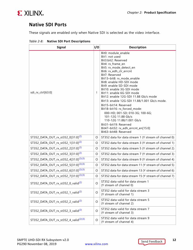
Native SDI PortsThese signals are enabled only when Native SDI is selected as the video interface.
Table 2-8: Native SDI Port DescriptionsSignal I/O Description
sdi_rx_ctrl[63:0] I
Bit0: module_enableBit1: not usedBit3:bit2: ReservedBit4: rx_frame_enBit5: rx_mode_detect_enBit6: rx_edh_clr_errcntBit7: ReservedBit13–bit8: rx_mode_enableBit8: enable HD-SDI modeBit9: enable SD-SDI modeBit10: enable 3G-SDI modeBit11: enable 6G-SDI modeBit12: enable 12G-SDI 11.88 Gb/s modeBit13: enable 12G-SDI 11.88/1.001 Gb/s mode. Bit15–bit14: ReservedBit18–bit16: rx_forced_mode:
000-HD; 001-SD; 010-3G; 100-6G; 101-12G 11.88 Gb/s110-12G 11.88/1.001 Gb/s
Bit31–bit19: ReservedBit47–bit32: rx_edh_errcnt_en[15:0]Bit63–bit48: Reserved
ST352_DATA_OUT_rx_st352_0[31:0](2) O ST352 data for data stream 1 (Y stream of channel 0)ST352_DATA_OUT_rx_st352_1[31:0](2) O ST352 data for data stream 3 (Y stream of channel 1)ST352_DATA_OUT_rx_st352_2[31:0](2) O ST352 data for data stream 5 (Y stream of channel 2)ST352_DATA_OUT_rx_st352_3[31:0](2) O ST352 data for data stream 7 (Y stream of channel 3)ST352_DATA_OUT_rx_st352_4[31:0](2)(3) O ST352 data for data stream 9 (Y stream of channel 4)ST352_DATA_OUT_rx_st352_5[31:0](2)(3) O ST352 data for data stream 11 (Y stream of channel 5)ST352_DATA_OUT_rx_st352_6[31:0](2)(3) O ST352 data for data stream 13 (Y stream of channel 6)ST352_DATA_OUT_rx_st352_7[31:0](2)(3) O ST352 data for data stream 15 (Y stream of channel 7)
ST352_DATA_OUT_rx_st352_0_valid(2) O ST352 data valid for data stream 1 (Y stream of channel 0)
ST352_DATA_OUT_rx_st352_1_valid(2) O ST352 data valid for data stream 3 (Y stream of channel 1)
ST352_DATA_OUT_rx_st352_2_valid(2) O ST352 data valid for data stream 5 (Y stream of channel 2)
ST352_DATA_OUT_rx_st352_3_valid(2) O ST352 data valid for data stream 7 (Y stream of channel 3)
ST352_DATA_OUT_rx_st352_4_valid(2)(3) O ST352 data valid for data stream 9(Y stream of channel 4)
Send Feedback

SMPTE UHD-SDI RX Subsystem v2.0 13PG290 November 08, 2019 www.xilinx.com
Chapter 2: Product Specification
ST352_DATA_OUT_rx_st352_5_valid(2)(3) O ST352 data valid for data stream 11(Y stream of channel 5)
ST352_DATA_OUT_rx_st352_6_valid(2)(3) O ST352 data valid for data stream 13(Y stream of channel 6)
ST352_DATA_OUT_rx_st352_7_valid(2)(3) O ST352 data valid for data stream 15 (Y stream of channel 7)
ST352_DATA_C_STR_OUT_rx_st352_0[31:0] O ST352 data valid for data stream 2 (C stream of channel 0)
ST352_DATA_C_STR_OUT_rx_st352_1[31:0] O
ST352 data valid for data stream 4(C stream of channel 1)Note:ST352_DATA_C_STR_OUT_rx_st352_1[31:0] has the same value as ST352_DATA_OUT_rx_st352_1[31:0] for 3G-SDI Level A
ST352_DATA_C_STR_OUT_rx_st352_2[31:0] O ST352 data for data stream 6 (C stream of channel 2) ST352_DATA_C_STR_OUT_rx_st352_3[31:0] O ST352 data for data stream 8 (C stream of channel 3)ST352_DATA_C_STR_OUT_rx_st352_4[31:0](3) O ST352 data for data stream 10 (C stream of channel 4)ST352_DATA_C_STR_OUT_rx_st352_5[31:0](3) O ST352 data for data stream 12 (C stream of channel 5)ST352_DATA_C_STR_OUT_rx_st352_6[31:0](3) O ST352 data for data stream 14 (C stream of channel 6)ST352_DATA_C_STR_OUT_rx_st352_7[31:0](3) O ST352 data for data stream 16 (C stream of channel 7)
ST352_DATA_C_STR_OUT_rx_st352_0_valid O ST352 data valid for data stream 2(C stream of channel 0)
ST352_DATA_C_STR_OUT_rx_st352_1_valid O ST352 data valid for data stream 4(C stream of channel 1)
ST352_DATA_C_STR_OUT_rx_st352_2_valid O ST352 data valid for data stream 6 (C stream of channel 2)
ST352_DATA_C_STR_OUT_rx_st352_3_valid O ST352 data valid for data stream 8(C stream of channel 3)
ST352_DATA_C_STR_OUT_rx_st352_4_valid O ST352 data valid for data stream 10(C stream of channel 4)
ST352_DATA_C_STR_OUT_rx_st352_5_valid O ST352 data valid for data stream 12 (C stream of channel 5)
ST352_DATA_C_STR_OUT_rx_st352_6_valid O ST352 data valid for data stream 14(C stream of channel 6)
ST352_DATA_C_STR_OUT_rx_st352_7_valid O ST352 data valid for data stream 16 (C stream of channel 7)
SDI_DS_OUT_ds1[9:0] O SDI data stream 1SDI_DS_OUT_ds2[9:0] O SDI data stream 2SDI_DS_OUT_ds3[9:0] O SDI data stream 3SDI_DS_OUT_ds4[9:0] O SDI data stream 4
Table 2-8: Native SDI Port Descriptions (Cont’d)
Signal I/O Description
Send Feedback

SMPTE UHD-SDI RX Subsystem v2.0 14PG290 November 08, 2019 www.xilinx.com
Chapter 2: Product Specification
SDI_DS_OUT_ds5[9:0] O SDI data stream 5SDI_DS_OUT_ds6[9:0] O SDI data stream 6SDI_DS_OUT_ds7[9:0] O SDI data stream 7SDI_DS_OUT_ds8[9:0] O SDI data stream 8SDI_DS_OUT_ln_num_1[10:0] to SDI_DS_OUT_ln_num_8 O SDI data stream line number
SDI_DS_OUT_rx_ce_out O Clock enable
SDI_DS_OUT_rx_active_streams O
This port indicates the number of data streams that are active for the current video format being received. The number of active data streams is 2^active_streams.000: 1 active stream001: 2 active streams010: 4 active streams011: 8 active streams
SDI_DS_OUT_rx_mode_locked O
When this output is Low, the receiver is actively searching for the SDI mode that matches the input data stream. During this time, the rx_mode_locked output port changes frequently.When the receiver locks to the correct SDI mode, the rx_mode_locked output goes High.
SDI_DS_OUT_rx_eav O This output is asserted High when the XYZ word of an EAV is present on the data stream output ports.
SDI_DS_OUT_rx_sav O This output is asserted High when the XYZ word of a SAV is present on the data stream output ports.
SDI_DS_OUT_rx_trs OThis output is asserted High while the four consecutive words of any EAV or SAV are present on the data stream output ports, from the 3FF word through the XYZ word.
SDI_DS_OUT_rx_mode_hd O High when RX is locked in HD-SDI modeSDI_DS_OUT_rx_mode_sd O High when RX is locked in SD-SDI modeSDI_DS_OUT_rx_mode_3g O High when RX is locked in 3G-SDI modeSDI_DS_OUT_rx_mode_6g O High when RX is locked in 6G-SDI modeSDI_DS_OUT_rx_mode_12g O High when RX is locked in 12G-SDI mode
SDI_DS_OUT_rx_level_b_3g OIN 3G-SDI mode, this output is asserted High when the input signal is level B and Low when it is level A. This output is only valid when rx_mode_3g is High.
Table 2-8: Native SDI Port Descriptions (Cont’d)
Signal I/O Description
Send Feedback

SMPTE UHD-SDI RX Subsystem v2.0 15PG290 November 08, 2019 www.xilinx.com
Chapter 2: Product Specification
Native Video Interface PortsThese ports are enable when the video interface is native video.
SDI_RX_ANC_DS_OUT Interface PortsThese ports are enabled when the Ancillary (ANC) Data Insertion I/F option is selected.
SDI_DS_OUT_sdi_mode[2:0] O
This output port indicates the current SDI mode of the receiver:000 = HD001 = SD010 = 3G100 = 6G101 = 12G 1000/1000110 = 12G 1000/1001When the receiver is not locked, the sdi_mode port changes values as the receiver searches for the correct SDI mode.During this time, the rx_mode_locked output is Low. When the receiver detects the correct SDI mode, the rx_mode_locked output goes High.
sdi_rx_err[31:0] O Bit15-bit0: rx_crc_err_ds16 to rx_crc_err_ds1Bit31-bit16: Reserved
Notes: 1. See the SMPTE UHD-SDI Product Guide (PG205) [Ref 9] for more detailed signal descriptions.2. Enabled only when the Enable AxiLite interface option is not selected in the Vivado IDE.3. Enabled only when 12G-SDI 16DS is selected as the SDI standard in the Vivado IDE.
Table 2-9: VID_IO_OUT Interface Port DescriptionsSignal I/O Description
VID_IO_OUT_data[59:0] O Native Video output dataVID_IO_OUT_active_video O Native Video active video outputVID_IO_OUT_field O Native Video field outputVID_IO_OUT_hblank O Native Video hblank outputVID_IO_OUT_vblank O Native Video vblank output
Table 2-10: SDI_RX_ANC_DS_OUT Interface Port DescriptionsSignal I/O Description
SDI_RX_ANC_DS_OUT_ds1[9:0] to SDI_TX_ANC_DS_OUT_ds8[9:0] O SDI stream outputs from 1 to 8
Table 2-8: Native SDI Port Descriptions (Cont’d)
Signal I/O Description
Send Feedback

SMPTE UHD-SDI RX Subsystem v2.0 16PG290 November 08, 2019 www.xilinx.com
Chapter 2: Product Specification
Register SpaceThis section details registers available in the SMPTE UHD-SDI RX Subsystem. The SMPTE UHD-SDI RX core has an address space of 64K.
SMPTE UHD-SDI RX RegistersThe SMPTE UHD-SDI RX registers are available when the AXI4-Lite Interface is selected in the Vivado IDE. The SMPTE UHD-SDI RX IP core register space is shown in Table 2-11.
IMPORTANT: This memory space must be aligned to an AXI word (32-bit) boundary.
All registers are in little endian format as shown in Figure 2-1.
SDI_RX_ANC_DS_OUT_ds9[9:0] to SDI_TX_ANC_DS_OUT_ds16[9:0] O SDI stream outputs from 9 to 16. Enabled only when
12 SDI 16 DS option is selected.
sdi_rx_anc_ctrl_out[31:0] O
Bit 0: rx_ce_outBit 3: Bit1: rx_modeBit 7: Bit4: rx_t_familyBit 8: rx_mode_lockedBit 9: rx_t_lockedBit 10 to 13: rx_t_rateBit 14: t_scanBit 15: SMPTE UHD-SDI RX IP internal resetBit 31:16: Reserved Available only when ANC data Insertion I/F option is selected
Table 2-10: SDI_RX_ANC_DS_OUT Interface Port Descriptions (Cont’d)
Signal I/O Description
X-Ref Target - Figure 2-1
Figure 2-1: 32-bit Little Endian Example
Table 2-11: SMPTE UHD-SDI RX IP Core Register Space
Offset Name Width Access Description
0x00 RST_CTRL 32-bit R/W Enable and soft reset controls for the IP core0x04 MODULE_CTRL 32-bit R/W Module control register0x08 RESERVED 32-bit N/A N/A
24 16 8 0
X21289-080918
Send Feedback

SMPTE UHD-SDI RX Subsystem v2.0 17PG290 November 08, 2019 www.xilinx.com
Chapter 2: Product Specification
0x0C GLBL_IER 32-bit R/W Global interrupt enable register0x10 ISR 32-bit R/W1C Interrupt status register0x14 IER 32-bit R/W Interrupt enable register0x18 RX_ST352_VALID 32-bit RO ST352 packet valid indication0x1C RX_ST352_DATA_DS1 32-bit RO Data stream 1 ST352 packet data0x20 RX_ST352_DATA_DS3 32-bit RO Data stream 3 ST352 packet data0x24 RX_ST352_DATA_DS5 32-bit RO Data stream 5 ST352 packet data0x28 RX_ST352_DATA_DS7 32-bit RO Data stream 7 ST352 packet data0x2C RX_ST352_DATA_DS9 32-bit RO Data stream 9 ST352 packet data0x30 RX_ST352_DATA_DS11 32-bit RO Data stream 11 ST352 packet data0x34 RX_ST352_DATA_DS13 32-bit RO Data stream 13 ST352 packet data0x38 RX_ST352_DATA_DS15 32-bit RO Data stream 15 ST352 packet data0x3C VERSION 32-bit RO Version Register0x40 SS_CONFIG 32-bit RO IP core Configuration0x44 MODE_DET_STS 32-bit RO Mode detect status0x48 TS_DET_STS 32-bit RO Transport Stream detect status0x4C RX_EDH_STS 32-bit RO EDH check status0x50 RX_EDH_ERRCNT_EN 32-bit R/W Enable EDH error count0x54 RX_EDH_ERRCNT 32-bit RO RX EDH error count 0x58 RX_CRC_ERR 32-bit RO RX CRC error indication0x5C VIDEO_LOCK_WINDOW 32-bit R/W Video lock window0x60 RESERVED 32-bit N/A N/A0x64 RESERVED 32-bit N/A N/A0x68 RESERVED 32-bit N/A N/A0x6C RESERVED 32-bit N/A N/A0x70 RX_ST352_DATA_DS2 32-bit RO Data stream 2 ST352 packet data0x74 RX_ST352_DATA_DS4 32-bit RO Data stream 4 ST352 packet data0x78 RX_ST352_DATA_DS6 32-bit RO Data stream 6 ST352 packet data0x7C RX_ST352_DATA_DS8 32-bit RO Data stream 8 ST352 packet data0x80 RX_ST352_DATA_DS10 32-bit RO Data stream 10 ST352 packet data0x84 RX_ST352_DATA_DS12 32-bit RO Data stream 12 ST352 packet data0x88 RX_ST352_DATA_DS14 32-bit RO Data stream 14 ST352 packet data
Table 2-11: SMPTE UHD-SDI RX IP Core Register Space (Cont’d)
Offset Name Width Access Description
Send Feedback

SMPTE UHD-SDI RX Subsystem v2.0 18PG290 November 08, 2019 www.xilinx.com
Chapter 2: Product Specification
RST_CTRL Register (0x00)This register allows you to enable and disable the SMPTE UHD-SDI RX IP core and apply a soft reset during core operation.
0x8C RX_ST352_DATA_DS16 32-bit RO Data stream 16 ST352 packet dataNotes: 1. Access type and reset value for all the reserved bits in the registers is read-only with value 0.2. Register accesses should be word aligned and there is no support for a write strobe. WSTRB is not used internally.3. Only the lower 7 bits (6:0) of the read and write address of the AXI4-Lite interface are decoded. This means that
accessing address 0x00 and 0x80 results in reading the same address of 0x00.4. Reads and writes to addresses outside this table do not return an error.
Table 2-12: RST_CTRL Register Bit Mapping
Bits Name Access Default Value Description
31:13 Reserved RO 0 Reserved
12:10 SDIRX_BRIDGE_CH_FORMAT_AXI R/W 0
Selection of chroma format001 - YUV 4:4:4 format selectionOthers - Reserved
9 VID_IN_AXI4S_MOD_EN R/W 0
Enable bit for Video-in-AXI4S core1 – Video-in-AXI4S core is enabled0 – Video-in-AXI4S core is disabledThis bit is available only in AXI4-Stream is selected as the video interface
8 SDIRX_BRIDGE_EN R/W 0
Enable bit for SDI RX Bridge1 – SDI RX bridge is enabled0 – SDI RX bridge is disabledThis bit is not available if Native SDI is selected as video interface
7:4 Reserved RO 0 Reserved3 RST_EDH_ERRCNT R/W 0 Clear rx_edh_errcnt register2 RST_CRC_ERRCNT R/W 0 Clear rx_crc_errcnt register
1 SRST R/W 0Soft reset for SDI RX IP coreWriting a 1 to this bit resets all registers of the SDI RX IP.
0 SDIRX_IP_EN R/W 0Enable bit for SDI RX IP core1 – SDI RX IP core is enabled0 – SDI RX IP core is disabled
Table 2-11: SMPTE UHD-SDI RX IP Core Register Space (Cont’d)
Offset Name Width Access Description
Send Feedback

SMPTE UHD-SDI RX Subsystem v2.0 19PG290 November 08, 2019 www.xilinx.com
Chapter 2: Product Specification
MODULE_CTRL Register (0x04)This register provides control of the SMPTE UHD-SDI RX IP core and core functional modes.
Global Interrupt Enable Register (GLBL_IER) (0x0C)
Table 2-13: MODULE_CTRL Register Bit Mapping
Bits Name Access Default Value Description
31:19 Reserved RO 0 Reserved
18:16 RX_FORCED_MODE R/W 0
RX forced mode3’b000: HD mode3’b001: SD mode3’b010: 3G mode3’b100: 6G mode3’b101: 12G mode with 11.88 Gb/s line rate3’b110: 12G mode with 11.88/1.001 Gb/s line rate
15:14 Reserved RO 0 Reserved
13:8 RX_MODE_EN R/W 0
RX mode enableBit8: enable HD-SDI modeBit9: enable SD-SDI modeBit10: enable 3G-SDI modeBit11: enable 6G-SDI modeBit12: enable 12G-SDI 11.88 Gb/s modeBit13: enable 12G-SDI 11.88/1.001 Gb/s mode
7:6 Reserved RO 2’b01 Reserved5 RX_MODE_DET_EN R/W 0 RX mode detection enable4 RX_FRM_EN R/W 0 RX frame enable
3:0 Reserved RO 0 Reserved
Table 2-14: GLBL_IER Register Bit Mapping
Bits Name Access Default Value Description
31:1 Reserved RO 0 Reserved
0 GLBL_INTRUPT_EN R/W 0
Master enable for the device interrupt output to the system1: Enabled—the corresponding Interrupt Enable register (IER) bits are used to generate interrupts0: Disabled—Interrupt generation blockedirrespective of IER bits
Send Feedback

SMPTE UHD-SDI RX Subsystem v2.0 20PG290 November 08, 2019 www.xilinx.com
Chapter 2: Product Specification
Interrupt Status Register (ISR) (0x10)This register captures the error and status information for the IP core.
Interrupt Enable Register (IER) (0x14)This register allows you to selectively generate an interrupt at the output port for each error/status bit in the ISR. An IER bit set to 0 does not inhibit an error/status condition from being captured, but inhibits it from generating an interrupt.
Table 2-15: ISR bit mapping
Bits Name Access(1) Default Value Description
31:11 Reserved RO 0 Reserved
10 UNDERFLOW_INTR R/W1C 0Video in to AXI4-Stream core underflow indication. This bit is available only in AXI4-Stream is selected as Video Interface.
9 OVERFLOW_INTR R/W1C 0Video in to AXI4-Stream core overflow indication. This bit is available only in AXI4-Stream is selected as Video Interface.
8:2 Reserved RO 0 Reserved
1 VIDEO_UNLOCK_INTR R/W1C 0 Asserted when incoming video pattern is unlocked
0 VIDEO_LOCK_INTR R/W1C 0Asserted when incoming video pattern islocked and ST352 Valid bit of Data Stream1 (RX_ST352_VLD_DS1 field) is asserted.
Notes: 1. W1C = Write 1 to clear.
Table 2-16: IER bit mapping
Bits Name Access Default Value Description
31:11 Reserved RO 0 Set bits in this register to 1 togenerate the required interrupts. Set to 0 to disable the interrupt.
For a description of the specific interrupt you are enabling/disabling in this register see the ISR descriptions in Table 2-15.
10 UNDERFLOW_INTR_EN R/W 09 OVERFLOW_INTR_EN R/W 0
8:2 Reserved RO 01 VIDEO_UNLOCK_INTR_EN R/W 00 VIDEO_LOCK_INTR_EN R/W 0
Send Feedback

SMPTE UHD-SDI RX Subsystem v2.0 21PG290 November 08, 2019 www.xilinx.com
Chapter 2: Product Specification
RX_ST352_VALID Register (0x18)Table 2-17: RX_ST352_VALID Register Bit Mapping
Bits Name Access DefaultValue Description
31:16 Reserved RO 0 Reserved
15 RX_ST352_VLD_DS16 RO 0 Asserted high when ST352 is valid on data stream 16 (C stream of Channel 7)
14 RX_ST352_VLD_DS14 RO 0 Asserted high when ST352 is valid on data stream 14 (C stream of Channel 6)
13 RX_ST352_VLD_DS12 RO 0 Asserted high when ST352 is valid on data stream 12 (C stream of Channel 5)
12 RX_ST352_VLD_DS10 RO 0 Asserted high when ST352 is valid on data stream 10 (C stream of Channel 4)
11 RX_ST352_VLD_DS8 RO 0 Asserted high when ST352 is valid on data stream 8 (C stream of Channel 3)
10 RX_ST352_VLD_DS6 RO 0 Asserted high when ST352 is valid on data stream 6 (C stream of Channel 2)
9 RX_ST352_VLD_DS4 RO 0 Asserted high when ST352 is valid on data stream 4 (C stream of Channel 1)
8 RX_ST352_VLD_DS2 RO 0 Asserted high when ST352 is valid on data stream 2 (C stream of Channel 0)
7 RX_ST352_VLD_DS15 RO 0 Asserted high when ST352 is valid on data stream 15 (Y stream of Channel 7)
6 RX_ST352_VLD_DS13 RO 0 Asserted high when ST352 is valid on data stream 13 (Y stream of Channel 6)
5 RX_ST352_VLD_DS11 RO 0 Asserted high when ST352 is valid on data stream 11 (Y stream of Channel 5)
4 RX_ST352_VLD_DS9 RO 0 Asserted high when ST352 is valid on data stream 9 (Y stream of Channel 4)
3 RX_ST352_VLD_DS7 RO 0 Asserted high when ST352 is valid on data stream 7 (Y stream of Channel 3)
2 RX_ST352_VLD_DS5 RO 0 Asserted high when ST352 is valid on data stream 5 (Y stream of Channel 2)
1 RX_ST352_VLD_DS3 RO 0 Asserted high when ST352 is valid on data stream 3 (Y stream of Channel 1)
0 RX_ST352_VLD_DS1 RO 0 Asserted high when ST352 is valid on data stream 1 (Y stream of Channel 0)
Send Feedback
SMPTE UHD-SDI RX Subsystem v2.0 22PG290 November 08, 2019 www.xilinx.com
Chapter 2: Product Specification
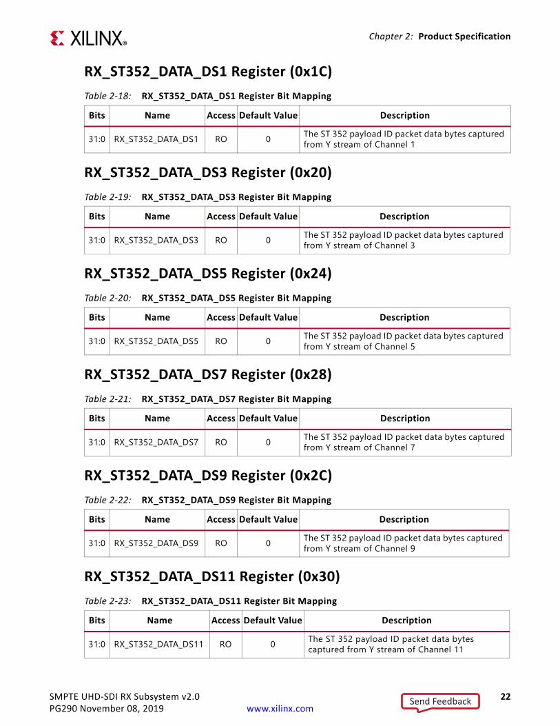
RX_ST352_DATA_DS1 Register (0x1C)
RX_ST352_DATA_DS3 Register (0x20)
RX_ST352_DATA_DS5 Register (0x24)
RX_ST352_DATA_DS7 Register (0x28)
RX_ST352_DATA_DS9 Register (0x2C)
RX_ST352_DATA_DS11 Register (0x30)
Table 2-18: RX_ST352_DATA_DS1 Register Bit Mapping
Bits Name Access Default Value Description
31:0 RX_ST352_DATA_DS1 RO 0 The ST 352 payload ID packet data bytes captured from Y stream of Channel 1
Table 2-19: RX_ST352_DATA_DS3 Register Bit Mapping
Bits Name Access Default Value Description
31:0 RX_ST352_DATA_DS3 RO 0 The ST 352 payload ID packet data bytes captured from Y stream of Channel 3
Table 2-20: RX_ST352_DATA_DS5 Register Bit Mapping
Bits Name Access Default Value Description
31:0 RX_ST352_DATA_DS5 RO 0 The ST 352 payload ID packet data bytes captured from Y stream of Channel 5
Table 2-21: RX_ST352_DATA_DS7 Register Bit Mapping
Bits Name Access Default Value Description
31:0 RX_ST352_DATA_DS7 RO 0 The ST 352 payload ID packet data bytes captured from Y stream of Channel 7
Table 2-22: RX_ST352_DATA_DS9 Register Bit Mapping
Bits Name Access Default Value Description
31:0 RX_ST352_DATA_DS9 RO 0 The ST 352 payload ID packet data bytes captured from Y stream of Channel 9
Table 2-23: RX_ST352_DATA_DS11 Register Bit Mapping
Bits Name Access Default Value Description
31:0 RX_ST352_DATA_DS11 RO 0 The ST 352 payload ID packet data bytes captured from Y stream of Channel 11
Send Feedback

SMPTE UHD-SDI RX Subsystem v2.0 23PG290 November 08, 2019 www.xilinx.com
Chapter 2: Product Specification
RX_ST352_DATA_DS13 Register (0x34)
RX_ST352_DATA_DS15 Register (0x38)
VERSION Register (0x3C)
SS_CONFIG Register (0x40)
Table 2-24: RX_ST352_DATA_DS13 Register Bit Mapping
Bits Name Access Default Value Description
31:0 RX_ST352_DATA_DS13 RO 0 The ST 352 payload ID packet data bytes captured from Y stream of Channel 13
Table 2-25: RX_ST352_DATA_DS15 Register Bit Mapping
Bits Name Access Default Value Description
31:0 RX_ST352_DATA_DS15 RO 0 The ST 352 payload ID packet data bytes captured from Y stream of Channel 15
Table 2-26: VERSION Register Bit Mapping
Bits Name Access Default Value Description
31:0 VERSION 32-bit 32’h02_00_0_0_00
For uhd_sdi_rx_ss_v1_0, VERSIONREGISTER is 32’h01_00_0_0_00.For uhd_sdi_rx_ss_v2_0, VERSIONREGISTER is 32’h02_00_0_0_00.• [31:24] - Subsystem major version.• [23:16] - Subsystem minor version.• [15:12] - Subsystem version revision.• [11:8] - Subsystem Patch details.• [7:0] - Internal revision.
Table 2-27: SS_CONFIG Register Bit Mapping
Bits Name Access Default Value Description
31:5 Reserved RO 0 Reserved4 ANC_IF RO 0 ANC Interface Enable
3:2 VID_INTF RO 0Video Interface2'b00: AXI4-Stream Interface2'b01: Native Video Interface2'b10: Native SDI
1 INC_RX_EDH_PROC RO 1 This bit will be set if the IP core generated with INCLUDE_RX_EDH_PROCESSOR
0 Reserved RO 0 Reserved
Send Feedback

SMPTE UHD-SDI RX Subsystem v2.0 24PG290 November 08, 2019 www.xilinx.com
Chapter 2: Product Specification
MODE_DET_STS Register (0x44)This register provides the SDI mode detection status.
TS_DET_STS Register (0x48)This register provides the transport stream detection status.
Table 2-28: ODE_DET_STS Register Bit Mapping
Bits Name Access Default Value Description
31:8 Reserved RO 0 Reserved
7 RX_3G_LEVEL_B RO 0 Asserted High when incoming stream is 3G-SDI level B
6:4 RX_ACT_STREAMS RO 1
RX active data streams3’b000: 1 active stream; 3’b001: 2 active streams (Default); 3’b010: 4 active streams; 3’b011: 8 active streams; 3’b100: 16 active streams;
3 RX_MODE_LOCKED RO 1RX mode locked indicationIf bit 5 of MODULE_CTRL is not set, then this bit will be set to 1’b1
2:0 RX_MODE RO 0
3’b000: HD-SDI Mode (default);3’b001: SD-SDI Mode;3’b010: 3G-SDI Mode;3’b100: 6G-SDI Mode; 3’b101: 12G-SDI 11.88 Gb/s Mode; 3’b110: 12G-SDI 11.88/1.001 Gb/s Mode;
Table 2-29: TS_DET_STS Register Bit Mapping
Bits Name Access Default Value Description
31:12 Reserved RO 0 Reserved
11:8 RX_T_RATE RO 0
This bit indicates the frame rate of the transport. This is not necessarily the same as the frame rate of the actual picture. This bit is only valid when RX_T_LOCKED is High.See Table 2-8 in the SMPTE UHD-SDI Product Guide (PG0205) [Ref 9] for details on the encoding of the bits.
7:4 RX_T_FAMILY RO 4’hF
This bit indicates which family of video signals is being used as the transport of the SDI. This bit is only valid when RX_T_LOCKED is High. This bit does not necessarily identify the video format of the picture being transported. It only identifies the transport characteristics.See Table 2-7 in the SMPTE UHD-SDI Product Guide (PG0205) [Ref 9] for details on the encoding of the bits.
3:2 Reserved RO 0 Reserved
Send Feedback

SMPTE UHD-SDI RX Subsystem v2.0 25PG290 November 08, 2019 www.xilinx.com
Chapter 2: Product Specification
RX_EDH_STS Register (0x4C)
1 RX_T_SCAN RO 0This bit indicates whether the transport is interlaced (Low) or progressive (High). This is not necessarily the same as the scan mode of the actual picture. This bit is only valid when RX_T_LOCKED is High
0 RX_T_LOCKED RO 0Asserted High when the transport detection function in the receiver has identified the transport format of the SDI signal.
Table 2-30: RX_EDH_STS Register Bit Mapping
Bits Name Access Default Value Description
31:23 Reserved RO 0 Reserved
22:19 RX_EDH_PKT_FLAGS RO 0This four error flags related to the most recently received EDH packet. See Table 2-5 in the SMPTE UHD-SDI Product Guide (PG0205) [Ref 9] for details on the encoding of the bits.
18:14 RX_EDH_ANC_FLAGS RO 0The ancillary error flag bits from the most recently received EDH packet. See Table 2-5 in the SMPTE UHD-SDI Product Guide (PG0205) [Ref 9] for details on the encoding of the bits.
13:9 RX_EDH_FF_FLAGS RO 0The full frame error flag bits from the most recently received EDH packet. See Table 2-5 in the SMPTE UHD-SDI Product Guide (PG0205) [Ref 9] for details on the encoding of the bits.
8:4 RX_EDH_AP_FLAGS RO 0The active picture error flag bits from the most recently received EDH packet. See Table 2-5 in the SMPTE UHD-SDI Product Guide (PG0205) [Ref 9] for details on the encoding of the bits.
3 Reserved RO 0 Reserved
2 RX_EDH_ANC RO 0 This output is asserted High when an ancillary data packet checksum error is detected.
1 RX_EDH_FF RO 0This bit is asserted High when the full field CRC calculated for the previous field does not match the FF CRC value in the EDH packet.
0 RX_EDH_AP RO 0This bit is asserted High when the active picture CRC calculated for the previous field does not match the AP CRC value in the EDH packet.
Table 2-29: TS_DET_STS Register Bit Mapping (Cont’d)
Bits Name Access Default Value Description
Send Feedback

SMPTE UHD-SDI RX Subsystem v2.0 26PG290 November 08, 2019 www.xilinx.com
Chapter 2: Product Specification
RX_EDH_ERRCNT_EN Register (0x50)
RX_EDH_ERRCNT Register (0x54)
RX_CRC_ERR Register (0x58)
Table 2-31: RX_EDH_ERRCNT_EN Register Bit Mapping
Bits Name Access Default Value Description
31:16 Reserved RO 0 Reserved15 EDH_PKT_CHKSUM_ERR R/W 0 EDH packet checksum-error14 AP_UES_ERR_EN R/W 0 AP UES error13 AP_IDA_ERR_EN R/W 0 AP IDA error12 AP_IDH_ERR_EN R/W 0 AP IDH error11 AP_EDA_ERR_EN R/W 0 AP EDA error10 AP_EDH_ERR_EN R/W 0 AP EDH error9 FF_UES_ERR_EN R/W 0 FF UES error8 FF_IDA_ERR_EN R/W 0 FF IDA error7 FF_IDH_ERR_EN R/W 0 FF IDH error6 FF_EDA_ERR_EN R/W 0 FF EDA error5 FF_EDH_ERR_EN R/W 0 FF EDH error4 ANC_UES_ERR_EN R/W 0 ANC UES error3 ANC_IDA_ERR_EN R/W 0 ANC IDA error2 ANC_IDH_ERR_EN R/W 0 ANC IDH error1 ANC_EDA_ERR_EN R/W 0 ANC EDA error0 ANC_EDH_ERR_EN R/W 0 ANC EDH error
Table 2-32: RX_EDH_ERRCNT Register Bit Mapping
Bits Name Access Default Value Description
31:16 Reserved RO 0 Reserved
15:0 RX_EDH_ERRCNT RO 0SD-SDI mode EDH error counter. It increments once per field when any of the error conditions enabled by the RX_EDH_ERRCNT_EN register bit(s) occur during that field.
Table 2-33: RX_CRC_ERR Register Bit Mapping
Bits Name Access(1) Default Value Description
31:16 RX_CRC_ERR_CNT RO 0 Cumulative CRC error count of data stream 1 to 1615 RX_CRC_ERR_DS16 R/W1C 0 CRC error indicator for each data stream 1614 RX_CRC_ERR_DS15 R/W1C 0 CRC error indicator for each data stream 15
Send Feedback

SMPTE UHD-SDI RX Subsystem v2.0 27PG290 November 08, 2019 www.xilinx.com
Chapter 2: Product Specification
VIDEO_LOCK_WINDOW Register (0x5C)
RX_ST352_DATA_DS2 Register (0x70)
RX_ST352_DATA_DS4 Register (0x74)
13 RX_CRC_ERR_DS14 R/W1C 0 CRC error indicator for each data stream 1412 RX_CRC_ERR_DS13 R/W1C 0 CRC error indicator for each data stream 1311 RX_CRC_ERR_DS12 R/W1C 0 CRC error indicator for each data stream 1210 RX_CRC_ERR_DS11 R/W1C 0 CRC error indicator for each data stream 119 RX_CRC_ERR_DS10 R/W1C 0 CRC error indicator for each data stream 108 RX_CRC_ERR_DS9 R/W1C 0 CRC error indicator for each data stream 97 RX_CRC_ERR_DS8 R/W1C 0 CRC error indicator for each data stream 86 RX_CRC_ERR_DS7 R/W1C 0 CRC error indicator for each data stream 75 RX_CRC_ERR_DS6 R/W1C 0 CRC error indicator for each data stream 64 RX_CRC_ERR_DS5 R/W1C 0 CRC error indicator for each data stream 5. 3 RX_CRC_ERR_DS4 R/W1C 0 CRC error indicator for each data stream 42 RX_CRC_ERR_DS3 R/W1C 0 CRC error indicator for each data stream 31 RX_CRC_ERR_DS2 R/W1C 0 CRC error indicator for each data stream 20 RX_CRC_ERR_DS1 R/W1C 0 CRC error indicator for each data stream 1
Notes: 1. W1C = Write 1 to clear.
Table 2-34: VIDEO_LOCK_WINDOW Register Bit Mapping
Bits Name Access Default Value Description
31:0 VIDEO_LOCK_WINDOW R/W 0 Number of rx_clk cycles of stable video before asserting video is locked
Table 2-35: RX_ST352_DATA_DS2 Register Bit MappingBits Name Access Default Value Description
31:0 RX_ST352_DATA_DS2 RO 0The ST 352 payload ID packet data bytes captured from data stream 2 (C stream of data channel 0)
Table 2-36: RX_ST352_DATA_DS4 Register Bit MappingBits Name Access Default Value Description
31:0 RX_ST352_DATA_DS4 RO 0The ST 352 payload ID packet data bytes captured from data stream 4 (C stream of data channel 1)
Table 2-33: RX_CRC_ERR Register Bit Mapping (Cont’d)
Bits Name Access(1) Default Value Description
Send Feedback

SMPTE UHD-SDI RX Subsystem v2.0 28PG290 November 08, 2019 www.xilinx.com
Chapter 2: Product Specification
RX_ST352_DATA_DS6 Register (0x78)
RX_ST352_DATA_DS8 Register (0x7C)
RX_ST352_DATA_DS10 Register (0x80)
RX_ST352_DATA_DS12 Register (0x84)
RX_ST352_DATA_DS14 Register (0x88)
Table 2-37: RX_ST352_DATA_DS6 Register Bit MappingBits Name Access Default Value Description
31:0 RX_ST352_DATA_DS6 RO 0The ST 352 payload ID packet data bytes captured from data stream 6(C stream of data channel 2)
Table 2-38: RX_ST352_DATA_DS8 Register Bit MappingBits Name Access Default Value Description
31:0 RX_ST352_DATA_DS8 RO 0The ST 352 payload ID packet data bytes captured from data stream 8(C stream of data channel 3)
Table 2-39: RX_ST352_DATA_DS10 Register Bit MappingBits Name Access Default Value Description
31:0 RX_ST352_DATA_DS10 RO 0The ST 352 payload ID packet data bytes captured from data stream 10(C stream of data channel 4)
Table 2-40: RX_ST352_DATA_DS12 Register Bit MappingBits Name Access Default Value Description
31:0 RX_ST352_DATA_DS12 RO 0The ST 352 payload ID packet data bytes captured from data stream 12(C stream of data channel 5)
Table 2-41: RX_ST352_DATA_DS14 Register Bit MappingBits Name Access Default Value Description
31:0 RX_ST352_DATA_DS14 RO 0The ST 352 payload ID packet data bytes captured from data stream 14(C stream of data channel 6)
Send Feedback

SMPTE UHD-SDI RX Subsystem v2.0 29PG290 November 08, 2019 www.xilinx.com
Chapter 2: Product Specification
RX_ST352_DATA_DS16 Register (0x8C)Table 2-42: RX_ST352_DATA_DS16 Register Bit Mapping
Bits Name Access Default Value Description
31:0 RX_ST352_DATA_DS16 RO 0The ST 352 payload ID packet data bytes captured from data stream 16(C stream of data channel 7)
Send Feedback

SMPTE UHD-SDI RX Subsystem v2.0 30PG290 November 08, 2019 www.xilinx.com
Chapter 3
Designing with the CoreThis chapter includes guidelines and additional information to facilitate designing with the core.
General Design GuidelinesThis section describes the steps required to turn a SMPTE UHD-SDI RX Subsystem into a fully functioning design with user-application logic.
IMPORTANT: Not all implementations require all of the design steps listed here. Follow the logic design guidelines in this manual carefully.
Use the Example Design as a Starting Point Each instance of a SMPTE UHD-SDI RX Subsystem that is created is delivered with an example design that can be implemented in Xilinx FPGA. This design can be used as a starting point for your own design or can be used to troubleshoot the user application, if necessary.
Know the Degree of Difficulty SMPTE UHD-SDI RX Subsystem design is challenging to implement in any technology, and the degree of difficulty is further influenced by:
• Maximum system clock frequency• Targeted device architecture• Nature of the user application
All SMPTE UHD-SDI RX Subsystem implementations require careful attention to system performance requirements. Pipelining, logic mappings, placement constraints and logic duplications are all methods that help boost system performance.
Send Feedback

SMPTE UHD-SDI RX Subsystem v2.0 31PG290 November 08, 2019 www.xilinx.com
Chapter 3: Designing with the Core
Keep It Registered To simplify timing and increase system performance in an FPGA design, keep all inputs and outputs registered with flip-flops between the user application and the subsystem. Registering signals might not be possible for all paths, but doing so simplifies timing analysis and makes it easier for the Xilinx tools to place-and-route the design.
Recognize Timing Critical Signals The XDC file provided with the example design for the core identifies the critical signals and the timing constraints that should be applied.
Make Only Allowed ModificationsThe SMPTE UHD-SDI RX Subsystem is not user modifiable. Any modifications might have adverse effects on the system timings and protocol compliance. Supported user configurations of the SMPTE UHD-SDI RX Subsystem can only be made by selecting options from the Vivado® Integrated Design Environment (IDE).
Clock Frequency SelectionThe SMPTE UHD-SDI RX Subsystem has multiple clock domains and has many CDC paths across the core. It is recommended to use the maximum allowed clock frequency to reduce the uncertainty due to clock domain crossing paths.
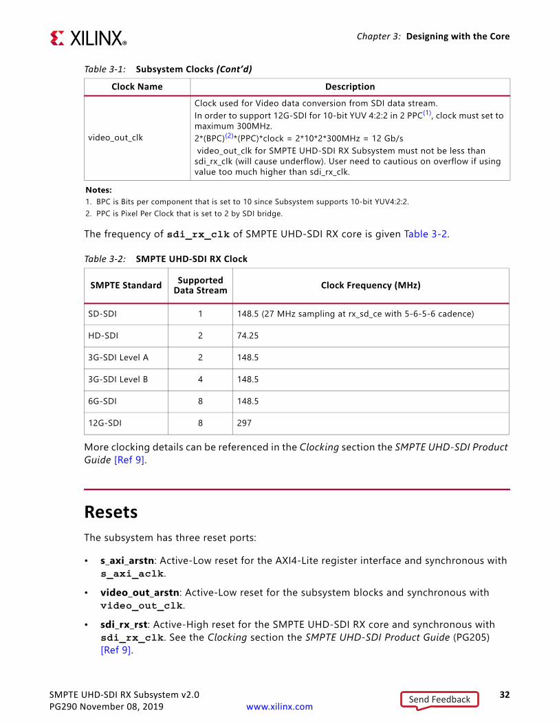
ClockingThe subsystem clocks are described in Table 3-1. Clock frequencies should be selected to match the throughput requirement and SDI standard.
Table 3-1: Subsystem ClocksClock Name Description
s_axi_aclk AXI4-Lite clock used by the register interface of all IP cores in the subsystem. Frequency range could be 50 MHz to 150 MHz
sdi_rx_clk Core clock for SMPTE UHD-SDI RX core. See Table 3-2 for more details.
Send Feedback
SMPTE UHD-SDI RX Subsystem v2.0 32PG290 November 08, 2019 www.xilinx.com
Chapter 3: Designing with the Core
The frequency of sdi_rx_clk of SMPTE UHD-SDI RX core is given Table 3-2.
More clocking details can be referenced in the Clocking section the SMPTE UHD-SDI Product Guide [Ref 9].
ResetsThe subsystem has three reset ports:
• s_axi_arstn: Active-Low reset for the AXI4-Lite register interface and synchronous with s_axi_aclk.
• video_out_arstn: Active-Low reset for the subsystem blocks and synchronous with video_out_clk.
• sdi_rx_rst: Active-High reset for the SMPTE UHD-SDI RX core and synchronous with sdi_rx_clk. See the Clocking section the SMPTE UHD-SDI Product Guide (PG205) [Ref 9].
video_out_clk
Clock used for Video data conversion from SDI data stream.In order to support 12G-SDI for 10-bit YUV 4:2:2 in 2 PPC(1), clock must set to maximum 300MHz.2*(BPC)(2)*(PPC)*clock = 2*10*2*300MHz = 12 Gb/s video_out_clk for SMPTE UHD-SDI RX Subsystem must not be less than sdi_rx_clk (will cause underflow). User need to cautious on overflow if using value too much higher than sdi_rx_clk.
Notes: 1. BPC is Bits per component that is set to 10 since Subsystem supports 10-bit YUV4:2:2.2. PPC is Pixel Per Clock that is set to 2 by SDI bridge.
Table 3-2: SMPTE UHD-SDI RX Clock
SMPTE Standard SupportedData Stream Clock Frequency (MHz)
SD-SDI 1 148.5 (27 MHz sampling at rx_sd_ce with 5-6-5-6 cadence)
HD-SDI 2 74.25
3G-SDI Level A 2 148.5
3G-SDI Level B 4 148.5
6G-SDI 8 148.5
12G-SDI 8 297
Table 3-1: Subsystem Clocks (Cont’d)
Clock Name Description
Send Feedback

SMPTE UHD-SDI RX Subsystem v2.0 33PG290 November 08, 2019 www.xilinx.com
Chapter 3: Designing with the Core
Table 3-3 summarizes all resets available to the SMPTE UHD-SDI RX Subsystem and the components affected by them.
Note: The effect of each reset (s_axi_arstn, video_out_arstn, sdi_rx_rst) is determined by the ports of the sub-cores to which they are connected. See the individual sub-core product guides for the effect of each reset signal. All the resets should be active until the associated clocks are stable.
UHD-SDI Audio Extract Use CaseThe SMPTE UHD-SDI RX Subsystem provides ANC I/F controlled by “Enable ANC Data (Incl. Audio) Extraction I/F” parameter in Vivado XGUI and can be used to extract the SDI audio from the SDI video stream. This section provides overview of extracting SDI audio from native SDI stream(s) using Xilinx UHD-SDI Audio IP core. For more information, see the UHD-SDI Audio LogiCORE IP Product Guide (PG309) [Ref 18]. The following figure shows the UHD-SDI Audio Extract use case.
The Xilinx UHD SDI Audio IP core is configurable as an audio embedder or an audio extractor. When configured as an audio extractor, it can extract up to 32 channels (16 channel pairs) of synchronous or asynchronous audio from the SDI stream.
Table 3-3: Core ResetsSub-Core s_axi_arstn video_out_arstn sdi_rx_rst
SMPTE UHD-SDI RX Connected to s_axi_aresetn core port
Connected to axis_rstn core port
Connected to rx_rst core port
SDI RX to Video Bridge N/A N/A Connected to rst core port
Video In to AXI4-Stream N/A N/A N/A
X-Ref Target - Figure 3-1
Figure 3-1: SMPTE UHD-SDI Audio Extract Use Case
Send Feedback

SMPTE UHD-SDI RX Subsystem v2.0 34PG290 November 08, 2019 www.xilinx.com
Chapter 3: Designing with the Core
It is designed in accordance with SMPTE ST 272 for SD-SDI and SMPTE ST 299 for HD SDI/3G-SDI/6G-SDI/12G-SDI to extract audio. It supports audio extraction at multiple audio sample rates (32 kHz, 44.1 kHz, and 48 kHz).
Functional DescriptionThe SD interface to the audio extractor consists of data streams, mode and status signals from the SMPTE UHD-SDI RX Subsystem. The audio interface is a 32-bit AXI4-Stream master bus. Figure 3-2 shows the top level block diagram of the SDI audio extractor in 32 channel configuration.
In SD-SDI mode, as per SMPTE ST 272, up to 16 channels of audio are extracted from data stream 1 (Y Video In). In HD-SDI mode, as per SMPTE ST 299-1, up to 16 channels of audio are extracted from data stream 1 and 2. In 3G-SDI, 6G-SDI and 12G-SDI modes, as per SMPTE ST 299-1 and SMPTE ST 299-2, up to 32 channels of audio are extracted from data streams 1, 2, 3, and 4. Audio control packets are extracted from data stream 1 and 3 (Y Video In) and data packets are extracted from data stream 2 and 4 (CBCR Video In).
The Xilinx AXI4-Stream audio interface carries audio samples in Audio Engineering Society (AES3) format. The data width over the AXI4-Stream audio interface is fixed at 32 bits to carry one AES3 sub-frame as shown in the following figure.
X-Ref Target - Figure 3-2
Figure 3-2: SDI Audio Extractor Block Diagram
Send Feedback

SMPTE UHD-SDI RX Subsystem v2.0 35PG290 November 08, 2019 www.xilinx.com
Chapter 3: Designing with the Core
The TID indicates the channel number of the audio sample data.
Figure 3-4 shows the interface timing diagram for the audio extractor core.
X-Ref Target - Figure 3-3
Figure 3-3: AES3 Subframe Format with 24-Bit Audio Sample
X-Ref Target - Figure 3-4
Figure 3-4: Audio Extract Timing Diagram
Send Feedback

SMPTE UHD-SDI RX Subsystem v2.0 36PG290 November 08, 2019 www.xilinx.com
Chapter 4
Design Flow StepsThis chapter describes customizing and generating the core, constraining the core, and the simulation, synthesis and implementation steps that are specific to this IP core. More detailed information about the standard Vivado® design flows in the IP Integrator can be found in the following Vivado Design Suite user guides:
• Vivado Design Suite User Guide: Designing IP Subsystems using IP Integrator (UG994) [Ref 1]
• Vivado Design Suite User Guide: Designing with IP (UG896) [Ref 2]• Vivado Design Suite User Guide: Getting Started (UG910) [Ref 3]• Vivado Design Suite User Guide: Logic Simulation (UG900) [Ref 4]
Customizing and Generating the CoreThis section includes information about using Xilinx tools to customize and generate the core in the Vivado® Design Suite.
Vivado Integrated Design Environment You can customize the IP for use in your design by specifying values for the various parameters associated with the IP core using the following steps:
1. Select the IP from the IP catalog.2. Double-click the selected IP or select the Customize IP command from the toolbar or
right-click menu.
For details, see the Vivado Design Suite User Guide: Designing with IP (UG896) [Ref 2] and the Vivado Design Suite User Guide: Getting Started (UG910) [Ref 3].
Note: Figures in this chapter are illustrations of the Vivado IDE. The layout depicted here might vary from the current version.
Send Feedback

SMPTE UHD-SDI RX Subsystem v2.0 37PG290 November 08, 2019 www.xilinx.com
Chapter 4: Design Flow Steps
Core Configuration TabFigure 4-1 shows the Core Configuration tab for customizing the SMPTE UHD-SDI RX Subsystem.
Component Name: The Component Name is the base name of the output files generated for this core.
IMPORTANT: The name must begin with a letter and be composed of the following characters: a to z, A to Z, 0 to 9 and "_."
Core Parameters• Video Interface: Specifies user interface. The available options are:
° AXI4-Stream (Default)
° Native Video
° Native SDI
X-Ref Target - Figure 4-1
Figure 4-1: Subsystem Configuration Tab
Send Feedback

SMPTE UHD-SDI RX Subsystem v2.0 38PG290 November 08, 2019 www.xilinx.com
Chapter 4: Design Flow Steps
• SDI Standard: Specifies the SDI standard. The available options are:
° 3G SDI
° 6G SDI
° 12G SDI 8DS (Default): 8 data streams
° 12G SDI 16DS (available only for Native SDI): 16 data streams
Application Example Design TabFigure 4-2 shows the Application Example Design tab for using the SMPTE UHD-SDI RX example design. See Chapter 5, Example Design for more information on the example design.
Target Board: Target board on which the Application example design to be built. The available options are:
• ZCU106 (Default)• KCU116
X-Ref Target - Figure 4-2
Figure 4-2: ZCU106 Pass-Through Application Example Design
Send Feedback

SMPTE UHD-SDI RX Subsystem v2.0 39PG290 November 08, 2019 www.xilinx.com
Chapter 4: Design Flow Steps
Design Topology: Type of configuration for application example design. The available options are:
• Pass-Through (Default)• Audio-Video Pass-Through• Audio-Video Loopback• RX-Only
User ParametersTable 4-1 shows the relationship between the fields in the Vivado IDE and the User Parameters (which can be viewed in the Tcl Console).
Output GenerationFor details, see the Vivado Design Suite User Guide: Designing with IP (UG896) [Ref 2].
Constraining the CoreThis section contains information about constraining the core in the Vivado Design Suite.
Table 4-1: Vivado IDE Parameter to User Parameter Relationship Vivado IDE Parameter to User Parameter Relationship
Vivado IDE Parameter/Value(1) User Parameter/Value Default ValueCore Parameters
Video Standard C_VIDEO_INTF AXI4-StreamSDI Standard C_LINE_RATE 12G SDI 8DSEnable ANC Data (Incl. Audio) Insertion Interface
C_INCLUDE_ADV_FEATURES FALSE
Enable AxiLite Interface C_INCLUDE_AXILITE TRUEInclude EDH Processor C_INCLUDE_EDH FALSETarget Board C_EXDES_BOARD ZCU106Design Topology C_EXEDES_CONFIG Pass-through
Notes: 1. Parameter values are listed in the table where the Vivado IDE parameter value differs from the user parameter
value. Such values are shown in this table as indented below the associated parameter.
Send Feedback

SMPTE UHD-SDI RX Subsystem v2.0 40PG290 November 08, 2019 www.xilinx.com
Chapter 4: Design Flow Steps
Required ConstraintsThis section defines the additional constraint requirements for the subsystem. Constraints are provided with a Xilinx Design Constraints (XDC) file. An XDC is provided with the HDL example design to give a starting point for constraints for your design.
Device, Package, and Speed Grade SelectionsThis section is not applicable for this subsystem.
Clock FrequenciesSee Clocking in Chapter 3.
Clock ManagementThe SMPTE UHD-SDI RX Subsystem generates the required clock constraints when generated using out-of-context mode with <component_name>_ooc.xdc. You can use these or update as required for other clock constraints.
Clock PlacementThis section is not applicable for this subsystem.
BankingThis section is not applicable for this subsystem.
Transceiver PlacementThis section is not applicable for this subsystem.
I/O Standard and PlacementThis section is not applicable for this subsystem.
Send Feedback

SMPTE UHD-SDI RX Subsystem v2.0 41PG290 November 08, 2019 www.xilinx.com
Chapter 4: Design Flow Steps
SimulationThis section contains information about simulating IP in the Vivado Design Suite. For comprehensive information about Vivado simulation components, as well as information about using supported third-party tools, see the Vivado Design Suite User Guide: Logic Simulation (UG900) [Ref 4].
Note: The SMPTE UHD-SDI RX Subsystem does not support simulation.
Synthesis and ImplementationThis section contains information about synthesis and implementation in the Vivado Design Suite. For details about synthesis and implementation, see the Vivado Design Suite User Guide: Designing with IP (UG896) [Ref 2].
Send Feedback

SMPTE UHD-SDI RX Subsystem v2.0 42PG290 November 08, 2019 www.xilinx.com
Chapter 5
Example DesignThis chapter contains information about the example design provided in the Vivado® Design Suite.
Table 5-1: Example Design Hardware Requirements
Topology Required Hardware ProcessorUHD-SDI GT
Configuration GTType
GTData
WidthBPC
TXPLL RXPLL
(Video)Pass-Through
• ZCU106• 2 HD-BNC to BNC cables • SDI source and sink devices
A53 QPLL1 QPLL0 GTHE4 40-bit 10
Audio-VideoPass-Through
SDI Audio Pass-Through° ZCU106 ° 2 HD-BNC to BNC cables° SDI source and sink devices
SDI Audio Playback to AES° ZCU106 ° 3 HD-BNC to BNC cables° SDI source and sink devices° AES Sink
AES capture to SDI TX° ZCU106° 3 HD-BNC to BNC cables° SDI source and sink devices° AES source
A53 QPLL1 QPLL0 GTHE4 40-bit 10
Audio-VideoLoopback
• KCU116• Fidus TB-FMCH-12GSDI SDI FMC• 1 HD-BNC to HD-BNC cable
MicroBlaze™ CPLL QPLL0(1)/QPLL1(2) GTYE4 40-bit 10
RX-Only• ZCU106• 1 HD-BNC to BNC cable• Sink device
A53 QPLL1 QPLL0 GTHE4 40-bit 10
Send Feedback

SMPTE UHD-SDI RX Subsystem v2.0 43PG290 November 08, 2019 www.xilinx.com
Chapter 5: Example Design
ZCU106 SMPTE UHD-SDI RX-Only Example DesignThe SMPTE UHD-SDI RX-only example design is built using the SMPTE UHD-SDI RX Subsystem. Video or image data is generated by test equipment and received by the SMPTE UHD-SDI RX Subsystem. The example design application software runs on the Zynq® UltraScale+™ MPSoC Arm processor system (PS) and is fully software controlled.
Note: The Zynq UltraScale+ MPSoC Arm PS is not shown in Figure 5-1.
ClockingQPLL0 is allocated for the SMPTE UHD-SDI RX transceiver in this RX-only example design. The QPLL0 reference clock is fixed to 148.5 MHz which comes from the on-board si570 chip. Figure 5-2 shows the clocking used in the SMPTE UHD-SDI RX-Only example design.
X-Ref Target - Figure 5-1
Figure 5-1: ZCU106 SMPTE UHD-SDI RX-Only Design
X-Ref Target - Figure 5-2
Figure 5-2: ZCU106 SMPTE UHD-SDI RX-Only Example Design Clocking
Send Feedback

SMPTE UHD-SDI RX Subsystem v2.0 44PG290 November 08, 2019 www.xilinx.com
Chapter 5: Example Design
Table 5-2 shows the clock frequency at various parts of the system for different SDI modes.
Transceiver Configuration in Example DesignThe UHD-SDI example design uses the UHD-SDI GT core to configure Xilinx® UltraScale+ GTH transceivers and provides options to the users to select the transceiver reference clocking. This core also generates control modules that are required to program the transceiver using the DRP interface.
Table 5-2: ZCU106 RX-Only Example Design Clock Frequency RangesSDI Mode Rx_m QPLL0 Refclk (MHz) rxoutclk (MHz)
SD-SDI N/A 148.5 148.5HD-SDI 0 148.5 74.25HD-SDI 1 148.5 74.25/1.001
3G-SDI/6G-SDI 0 148.5 148.53G-SDI/6G-SDI 1 148.5 148.5/1.001
12G-SDI 0 148.5 29712G-SDI 1 148.5 297/1.001
Notes: 1. rx_m or tx_m represents integer line rate when it is set to 0 and it represents fractional line rate when it is set to 1.
Send Feedback

SMPTE UHD-SDI RX Subsystem v2.0 45PG290 November 08, 2019 www.xilinx.com
Chapter 5: Example Design
Running the ZCU106 RX-Only Example Design1. Open the Vivado Design Suite and create a new project.2. In the pop-up window, press Next five times.3. Select the ZCU106 board.
4. Click Finish.5. Click IP Catalog and select SMPTE UHD-SDI RX Subsystem under Video Connectivity,
and then double click SMPTE UHD-SDI RX Subsystem.
Send Feedback

SMPTE UHD-SDI RX Subsystem v2.0 46PG290 November 08, 2019 www.xilinx.com
Chapter 5: Example Design
Note: For the application example design flow, the IP configuration is based on options selected in Application Example Design tab. You can rename the IP component name, which is used as the application example design project name.6. Configure the SMPTE UHD-SDI RX Subsystem Application Example Design tab by
selecting ZCU106 as the Target Board followed by RX-Only as Design Topology and click OK.
7. Click Generate.Note: You can optionally click Skip if you only want to generate the application example design.
Send Feedback

SMPTE UHD-SDI RX Subsystem v2.0 47PG290 November 08, 2019 www.xilinx.com
Chapter 5: Example Design
8. Right click the SMPTE UHD-SDI RX Subsystem component under Design source, and click Open IP Example Design.
The IP integrator design is then generated and creates the Vitis™ software platform. You can choose to Run Synthesis, Implementation, or Generate Bitstream. Figure 5-3 is an overall system IP integrator block diagram of the ZCU106-based application example design.
RequirementsHardware
The hardware requirements for this reference system are:• One Xilinx Zynq UltraScale+ MPSoC ZCU106 Evaluation Kit• One SDI source equipment• One HD-BNC to BNC converter cable
Software
This section includes any software requirements:• Vivado Design Suite 2019.2 or later • The Vitis software platform 2019.2 • Software terminals (for example, Tera Term, HyperTerminal or PuTTY)• SCUI may be required for some versions of the FMC card to set the power rail to 1.8v
X-Ref Target - Figure 5-3
Figure 5-3: IP Integrator Diagram of the ZCU106 RX-Only Application Example Design
Send Feedback

SMPTE UHD-SDI RX Subsystem v2.0 48PG290 November 08, 2019 www.xilinx.com
Chapter 5: Example Design
SetupThis reference design runs on the Zynq UltraScale+ MPSoC board (ZCU106) using SDI connectors available on the board. Additional information about the ZCU106 board can be found on the product page.
Follow these instructions to set up:
1. Connect a USB cable from the host PC to the USB JTAG port (1). Ensure the appropriate device drivers are installed.
2. Connect a second USB cable from the host PC to the USB UART port (2). Ensure that the USB UART drivers described in Hardware have been installed.
3. Connect the SDI_IN link of ZCU106 (3) to the SDI source device.4. Connect the ZCU106 board to a power supply slot (4).5. Switch on the ZCU106 board (5).6. Make sure that the HW-ZCU106 board revision (6) is Rev C.7. Start Tera Term or PuTTY to connect to the COM port interface 0 on the Host PC with
115200 bps, 8 bits, No parity, 1 stop bit, and no flow control as configuration.8. When using FMC card, set the FMC_VADJ voltage to 1.8V.Note: The numbers in the parenthesis in the instructions correspond to the callouts in Figure 5-4.
X-Ref Target - Figure 5-4
Figure 5-4: ZCU106 Board Setup
Send Feedback

SMPTE UHD-SDI RX Subsystem v2.0 49PG290 November 08, 2019 www.xilinx.com
Chapter 5: Example Design
Compiling Software in the Vitis Software PlatformThe UHD-SDI application example design generates a .elf file automatically. Follow the steps if you want to open the Vitis software platform project for the UHD-SDI example design from the Vivado Design Suite:
1. In the Vivado Design Suite, click Tools > Launch Vitis.2. Select Exported location and workspace as <Proj Dir>/SW/xsdi_app and click OK
to launch and open the Vitis software platform project.
The Vitis software platform project is now open.
Running the design on the hardwareThe following steps are used to run the BIT and ELF files on the hardware setup:
1. Connect the JTAG cable and USB-UART cable to the board.2. Go to <Component Name>_ex/imports.3. Start the Xilinx Software Debugger (XSDB) by sourcing xsdb from the build area to the
command prompt.4. Run the following command, source xsdb.tcl, to program FPGA and to execute the
application.5. To observe the results, open Tera Term or PUTTY, and configure the serial port (Interface
0) to 115200 baud with the default configuration. Note: Make sure that the UART cable is connected to the board and the PC.
The UART console now displays the SDI stream details on the console.
Send Feedback

SMPTE UHD-SDI RX Subsystem v2.0 50PG290 November 08, 2019 www.xilinx.com
Chapter 5: Example Design
UART Console ScreensThe following screen capture shows initial UART console output along with menu options.X-Ref Target - Figure 5-5
Figure 5-5: UART Console - Received UHD SDI Stream Information
Send Feedback

SMPTE UHD-SDI RX Subsystem v2.0 51PG290 November 08, 2019 www.xilinx.com
Chapter 5: Example Design
The following screen capture shows UART console output when resolution is changed at SDI source.X-Ref Target - Figure 5-6
Figure 5-6: UART Console - Received UHD SDI Stream Information after RX Mode Change
Send Feedback

SMPTE UHD-SDI RX Subsystem v2.0 52PG290 November 08, 2019 www.xilinx.com
Chapter 5: Example Design
ZCU106 SMPTE UHD-SDI Pass-Through Example DesignThe UHD-SDI pass-through example design, shown in Figure 5-7, is built using the SMPTE UHD-SDI TX and RX subsystems. Video or image data is received and processed by the SMPTE UHD-SDI RX Subsystem. The clock is recovered by the Xilinx® UltraScale™+ GTH transceiver (RX) and fed to the on-board PLL for jitter attenuation. A jitter-attenuated clock is used as a reference clock by the GTH transceiver for the TX data path. An AXI4-Stream FIFO is used for synchronization and temporary storage between the SMPTE UHD-SDI RX Subsystem and the SMPTE UHD-SDI TX Subsystem. The SMPTE UHD-SDI TX Subsystem transmits SDI data from the AXI4-Stream FIFO after the application programs the SMPTE UHD-SDI TX Subsystem sub-core registers based on the received SDI stream and ST-352 payload packet data. The example design application software runs on the Zynq UltraScale+ MPSoC Arm processor subsystem (PS) and is fully software controlled.
Note: The Zynq UltraScale+ MPSoC PS is not shown in Figure 5-7 for simplicity.
ClockingQPLL0 is allocated for the SMPTE UHD-SDI RX transceiver and QPLL1 for the SMPTE UHD-SDI TX in this pass-through design. The reference clock for QPLL1 comes from the si5328 chip output. Thus, the QPLL1 reference clock connection is fixed. The QPLL0 reference clock is fixed at 148.5 MHz and comes from the on-board si570 chip. Figure 5-8 shows the clocking used in the SMPTE UHD-SDI example design.
X-Ref Target - Figure 5-7
Figure 5-7: ZCU106 Pass-Through Example DesignX21408-110618
Send Feedback

SMPTE UHD-SDI RX Subsystem v2.0 53PG290 November 08, 2019 www.xilinx.com
Chapter 5: Example Design
Table 5-3 shows the clock frequency at different part of the system for different SDI modes:
Note: For 6G-SDI and 12G-SDI, 8 native SDI Data Streams (DS) is assumed.
For GT TX and RX data path, the reference clock requirement for data paths are different. For GT TX, for integer and fractional frame rate, PLL reference clock must be different frequency, clock/1.000 for integer frame rate and clock/1.001 for fractional frame rate. For RX data path PLL reference clock can be same for integer and fractional frame rate.
X-Ref Target - Figure 5-8
Figure 5-8: ZCU106 Pass-Through Example Design Clocking
Table 5-3: ZCU106 Pass-Through Example Design Clock Frequency Ranges
SDI Mode Tx_m/Rx_m
QPLL0Ref clk(MHz)
QPLL1Ref Clk(MHz)
rxoutclk(MHz)
si5328Input(MHz)
si5328Output(MHz)
txoutclk(MHz)
SD-SDI N/A 148.5 148.5 148.5rx_sd_ce=27 rx_sd_ce=27 148.5 148.5
HD-SDI 0 148.5 148.5 74.25 74.25 74.25 74.25HD-SDI 1 148.5 148.5/1.001 74.25/1.001 74.25/1.001 74.25/1.001 74.25/1.0013G-SDI/6G-SDI 0 148.5 148.5 148.5 148.5 148.5 148.53G-SDI/6G-SDI 1 148.5 148.5/1.001 148.5/1.001 148.5/1.001 148.5/1.001 148.5/1.00112G-SDI 0 148.5 148.5 297 297 148.5 29712G-SDI 1 148.5 148.5/1.001 297/1.001 297/1.001 148.5/1.001 297/1.001
Send Feedback

SMPTE UHD-SDI RX Subsystem v2.0 54PG290 November 08, 2019 www.xilinx.com
Chapter 5: Example Design
Transceiver Configuration in Example DesignThe UHD-SDI example design uses uhdsdi_gt_v2_0 core to configure UltraScale+ GTH transceivers and provide options to select the transceiver reference clocking. The core also generates control modules that are required to program the transceiver using DRP interface and NI-DRU modules for RX SD-SDI mode.
Running the ZCU106 Pass-Through Example Design1. Open the Vivado Design Suite and create a new project.2. In the pop-up window, press Next 3 times.
Send Feedback

SMPTE UHD-SDI RX Subsystem v2.0 55PG290 November 08, 2019 www.xilinx.com
Chapter 5: Example Design
3. Select the ZCU106 Board.
4. Click Finish.5. Click IP Catalog and double-click SMPTE UHD-SDI RX Subsystem under Video
Connectivity.
Send Feedback

SMPTE UHD-SDI RX Subsystem v2.0 56PG290 November 08, 2019 www.xilinx.com
Chapter 5: Example Design
For the application example design flow, the IP configuration is based on options selected in the Application Example Design tab.
You can rename the IP component name, which is used as the application example design project name.
Configure the SMPTE UHD-SDI RX Subsystem Application Example Design tab and click OK.
The Generate Output Products dialog box appears
6. Click Generate. a. You can optionally click Skip if you only want to generate the application example
design.
Send Feedback

SMPTE UHD-SDI RX Subsystem v2.0 57PG290 November 08, 2019 www.xilinx.com
Chapter 5: Example Design
7. Right-click the SMPTE UHD-SDI RX Subsystem component under Design source, and click Open IP Example Design.
Send Feedback

SMPTE UHD-SDI RX Subsystem v2.0 58PG290 November 08, 2019 www.xilinx.com
Chapter 5: Example Design
8. Choose the target project location, then click OK.
The IP integrator design is then generated and creates the Vitis software platform generates a .elf file. You can choose to Run Synthesis, Implementation, or Generate Bitstream. An overall system IP integrator block diagram of the ZCU106-based application example design is shown in Figure 5-9.
X-Ref Target - Figure 5-9
Figure 5-9: IP Integrator Diagram of the ZCU106 Pass-Through Example Design
Send Feedback

SMPTE UHD-SDI RX Subsystem v2.0 59PG290 November 08, 2019 www.xilinx.com
Chapter 5: Example Design
Requirements
Hardware
The hardware requirements for this reference system are:
• Xilinx Zynq UltraScale+ MPSoC ZCU106 Evaluation Kit• SDI source equipment • SDI sink equipment• Two HD_BNC to BNC converter cables
Software
This section includes any software requirements:
• Vivado Design Suite 2019.2 or later • The Vitis software platform 2019.2• Software terminals (for example, Tera Term, HyperTerminal or PuTTY)
Setup
The reference design runs on the Zynq UltraScale+ MPSoC board (ZCU106) using SDI connectors available on the board.
Send Feedback

SMPTE UHD-SDI RX Subsystem v2.0 60PG290 November 08, 2019 www.xilinx.com
Chapter 5: Example Design
In the following procedure, the numbers in parentheses correspond to the callout numbers in Figure 5-10.
1. Connect a USB cable from the host PC to the USB JTAG port (1). Ensure the appropriate device drivers are installed.
2. Connect a second USB cable from the host PC to the USB UART port (2). Ensure that the USB UART drivers described in Hardware have been installed.
3. Connect the SDI_INT link of ZCU106 (3) to the SDI source device.4. Connect the SDI_OUT link of ZCU106 (4) to the SDI sink device.5. Connect the ZCU106 board to a power supply slot (5).6. Switch on the ZCU106 board (6).7. Make sure that the HW-ZCU106 board revision (7) is Rev C.8. Ensure that the SMPTE 352/Payload ID is enabled in the SDI Stream connected to the SDI
input link of ZCU106.9. Start Tera Term or PuTTY to connect to the COM port interface 0 on the Host PC with
115200 bps, 8 bits, No parity, 1 stop bit, and no flow control as configuration.
X-Ref Target - Figure 5-10
Figure 5-10: ZCU106 Board Setup
Send Feedback

SMPTE UHD-SDI RX Subsystem v2.0 61PG290 November 08, 2019 www.xilinx.com
Chapter 5: Example Design
Compiling Software in VitisThe UHD-SDI application example design generates a .elf file automatically. Use the following procedure if you want to open the SDK project for the UHD-SDI example design from the Vivado Design Suite:
1. In the Vivado Design Suite, click Tools > Launch Vitis.2. Select Exported location and workspace as <Proj Dir>/SW/xsdi_app and click OK
to launch and open the Vitis software platform project.
Vitis software platform project opens.
Running the Design on the HardwareThe following steps are used to run the BIT and ELF files on the hardware setup:
1. Connect the JTAG cable and USB-UART cable to the board.2. Navigate to <Component Name>_ex/imports.3. Start the Xilinx Software Debugger (XSDB) by sourcing xsdb from the build area using
command prompt.4. Run the following command to program FPGA and to execute the application.
source xsdb.tcl
5. To observe the results, open Tera Term or PUTTY and configure its serial port (Interface 0) to 115200 baud with the default configuration. Make sure that the UART cable is connected to the board and the PC.
The UART console displays SDI stream details on console.
Send Feedback
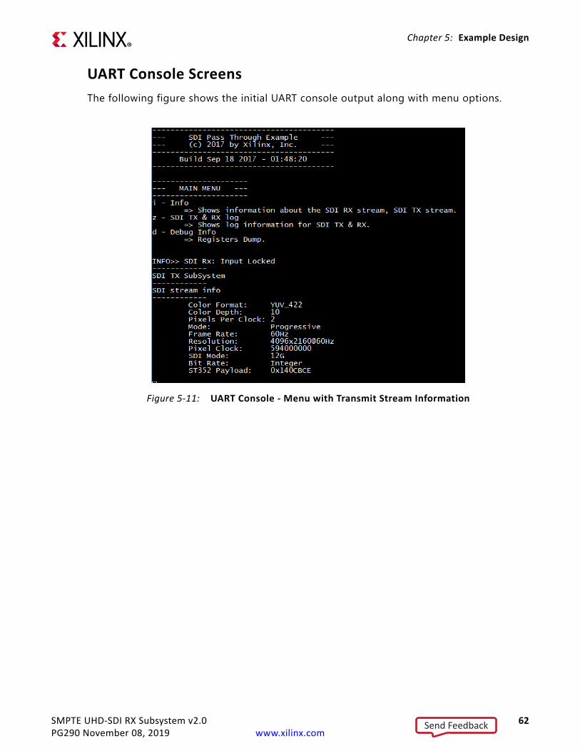
SMPTE UHD-SDI RX Subsystem v2.0 62PG290 November 08, 2019 www.xilinx.com
Chapter 5: Example Design
UART Console ScreensThe following figure shows the initial UART console output along with menu options.X-Ref Target - Figure 5-11
Figure 5-11: UART Console - Menu with Transmit Stream Information
Send Feedback

SMPTE UHD-SDI RX Subsystem v2.0 63PG290 November 08, 2019 www.xilinx.com
Chapter 5: Example Design
The following figure shows the UART console output when i is pressed.X-Ref Target - Figure 5-12
Figure 5-12: UART Console - Receive and Transmit UHD SDI Stream Information
Send Feedback

SMPTE UHD-SDI RX Subsystem v2.0 64PG290 November 08, 2019 www.xilinx.com
Chapter 5: Example Design
The following screen appears in the console output when z is pressed.
The following screen appears in the console output when d is pressed:
X-Ref Target - Figure 5-13
Figure 5-13: UART Console - Initialization Screen
X-Ref Target - Figure 5-14
Figure 5-14: UART Console - Register Dump for Debugging
Send Feedback

SMPTE UHD-SDI RX Subsystem v2.0 65PG290 November 08, 2019 www.xilinx.com
Chapter 5: Example Design
ZCU106 SMPTE UHD-SDI Audio-Video Pass-Through Example DesignThe UHD-SDI Audio-Video Pass-through example design, shown in Figure 5-15, is built using UHD-SDI TX and RX Subsystems along with UHD-SDI Audio and SPDIF/AES3 IP cores.
Note: The Zynq UltraScale+ MPSoC PS is not shown in Figure 5-8 for simplicity.
Video Processing PathVideo or image data with audio is received and processed by the SMPTE UHD-SDI RX Subsystem. The clock is recovered by the Xilinx® UltraScale™+ GTH transceiver (RX) and fed to the on-board PLL for jitter attenuation. A jitter-attenuated clock is used as a reference clock by the GTH transceiver for the TX data path. An AXI4-Stream FIFO is used for synchronization and temporary storage between the SMPTE UHD-SDI RX Subsystem and the UHD-SDI TX Subsystem. The UHD-SDI TX Subsystem transmits SDI data from the AXI4-Stream FIFO after the application programs the UHD-SDI TX Subsystem sub-core registers based on the received SDI stream and the ST-352 payload packet data.
X-Ref Target - Figure 5-15
Figure 5-15: ZCU106 Audio-Video Pass-Through Design
UHD-SDI GT CTRL Logic
FPGA
X21411-090518
Send Feedback

SMPTE UHD-SDI RX Subsystem v2.0 66PG290 November 08, 2019 www.xilinx.com
Chapter 5: Example Design
Audio Processing PathThis example design supports one of the two modes listed below based on the user input. Initially, the system comes up with SDI Audio Pass-through mode. You can switch to AES3 Audio Capture and Playback mode by pressing a on the UART terminal.
SDI Audio Pass-through
In this mode, up to 32 channels of audio can be extracted by the UHD-SDI Audio (Extract) IP. Audio received from the RX data path is embedded into the native SDI stream by the UHD-SDI Audio (Embed) IP. An AXI4-Stream FIFO is used for temporary storage between the UHD-SDI Audio (Extract) and the UHD-SDI Audio (Embed) IP.
AES3 Audio Capture and Playback
In this mode, up to 32 channels of audio can be extracted by the UHD-SDI Audio (Extract) IP. Channels 1 and 2 of the extracted audio are sent to the SPDIF/AES3 TX IP for AES playback.
The Audio Clock Recovery (ACR) IP is used to generate the audio sample rate clock (48 kHz, 44.1 kHz, or 32 kHz) from the SDI RX video clock. Application software programs the N and CTS values in the ACR IP, based on the SDI RX mode and the audio sample rate provided by the UHD-SDI Audio (Extract) IP. The ACR IP tracks the SPDIF/AES3 TX FIFO data count to adjust the sample rate clock to avoid FIFO overflow or underflow resulting in dropping or insertion of null samples. The sample rate clock from the ACR is fed to the on-board PLL for generating the audio clock (Fs*512) for the SPDIF/AES3 TX IP. On the other hand, Audio captured from the AES input is embedded on to the SDI TX.
The example design application software runs on the Zynq UltraScale+ MPSoC Arm processor subsystem (PS) and is fully software controlled.
ClockingQPLL0 is allocated for UHD-SDI RX transceiver and QPLL1 for UHD-SDI TX in this pass-through design. The reference clock for QPLL1 comes from si5328 chip output. Thus, QPLL1 reference clock connection is fixed. QPLL0 reference clock is fixed to 148.5 MHz which comes from on-board si570 chip. Figure 5-8 shows the clocking used in the UHD-SDI example design.
Send Feedback

SMPTE UHD-SDI RX Subsystem v2.0 67PG290 November 08, 2019 www.xilinx.com
Chapter 5: Example Design
Table 5-3 shows the clock frequency at different part of the system for different SDI modes:
Note: For 6G-SDI and 12G-SDI, 8 native SDI Data Streams (DS) is assumed.
For GT TX and RX data path, the reference clock requirement for data paths are different. For GT TX, for integer and fractional frame rate, PLL reference clock must be different frequency, clock/1.000 for integer frame rate and clock/1.001 for fractional frame rate. For RX data path PLL reference clock can be same for integer and fractional frame rate up to 6-G SDI and separate reference clock is required for 12-G SDI integer and fractional frame rate.
X-Ref Target - Figure 5-16
Figure 5-16: ZCU106 Audio-Video Pass-Through Example Design Clocking
Table 5-4: ZCU106 Audio-Video Example Design Clock Frequency Ranges
SDI Mode Tx_m/Rx_m
QPLL0Ref clk(MHz)
QPLL1Ref Clk(MHz)
txoutclk(MHz)
si5328Input(MHz)
si5328Output(MHz)
txoutclk(MHz)
SD-SDI N/A 148.5 148.5 148.5rx_sd_ce=27 rx_sd_ce=27 148.5 148.5
HD-SDI 0 148.5 148.5 74.25 74.25 74.25 74.25HD-SDI 1 148.5 148.5/1.001 74.25/1.001 74.25/1.001 74.25/1.001 74.25/1.0013G-SDI/6G-SDI 0 148.5 148.5 148.5 148.5 148.5 148.53G-SDI/6G-SDI 1 148.5 148.5/1.001 148.5/1.001 148.5/1.001 148.5/1.001 148.5/1.00112G-SDI 0 148.5 148.5 297 297 148.5 29712G-SDI 1 148.5 148.5/1.001 297/1.001 297/1.001 148.5/1.001 297/1.001
Send Feedback

SMPTE UHD-SDI RX Subsystem v2.0 68PG290 November 08, 2019 www.xilinx.com
Chapter 5: Example Design
Transceiver Configuration in Example DesignThe UHD-SDI example design uses the uhdsdi_gt_v2_0 core to configure UltraScale+ GTH transceivers and provide options to select the transceiver reference clocking. The core also generates control modules that are required to program the transceiver using DRP interface and NI-DRU modules for RX SD-SDI mode.
Running the ZCU106 Audio-Video Pass-Through Example Design1. Open the Vivado Design Suite and create a new project.2. In the pop-up window, press Next 5 times.3. Select the ZCU106 Board.
4. Click Finish.
Send Feedback

SMPTE UHD-SDI RX Subsystem v2.0 69PG290 November 08, 2019 www.xilinx.com
Chapter 5: Example Design
5. In the IP Catalog double-click SMPTE UHD-SDI RX Subsystem under Video Connectivity.
Note: For the application example design flow, the IP configuration is based on options selected in the Application Example Design tab. You can rename the IP component name, which is used as the application example design project name.6. Configure the SMPTE UHD-SDI RX Subsystem Application Example Design tab by
selecting ZCU106 as the Target Board followed by Audio-Video Pass-Through as Design Topology and click OK.
The Generate Output Products dialog box appears
7. Click Generate.Note: Click Skip if you only want to generate the application example design.
Send Feedback

SMPTE UHD-SDI RX Subsystem v2.0 70PG290 November 08, 2019 www.xilinx.com
Chapter 5: Example Design
8. Right click the SMPTE UHD-SDI RX Subsystem component under Design source, and click Open IP Example Design.
9. Choose the target project location and click OK.
The IP integrator design is then generated and creates the Vitis software platform and generates a .elf file. You can choose to Run Synthesis, Implementation, or Generate Bitstream. An overall system IP integrator block diagram of the ZCU106-based application example design is shown here.
Send Feedback

SMPTE UHD-SDI RX Subsystem v2.0 71PG290 November 08, 2019 www.xilinx.com
Chapter 5: Example Design
Requirements
Hardware
The hardware requirements for this reference system are:
• Xilinx Zynq UltraScale+ MPSoC ZCU106 Evaluation Kit• SDI source equipment • SDI sink equipment• Four HD-BNC to BNC converter cables• AES source equipment• AES sink equipment
Software
This section includes any software requirements:
• Vivado Design Suite 2019.2 or later • The Vitis software platform 2019.2• Software terminals (for example, Tera Term, HyperTerminal or PuTTY)
X-Ref Target - Figure 5-17
Figure 5-17: IP Integrator Diagram of the ZCU106 Audio-Video Pass-Through Example Design
Send Feedback
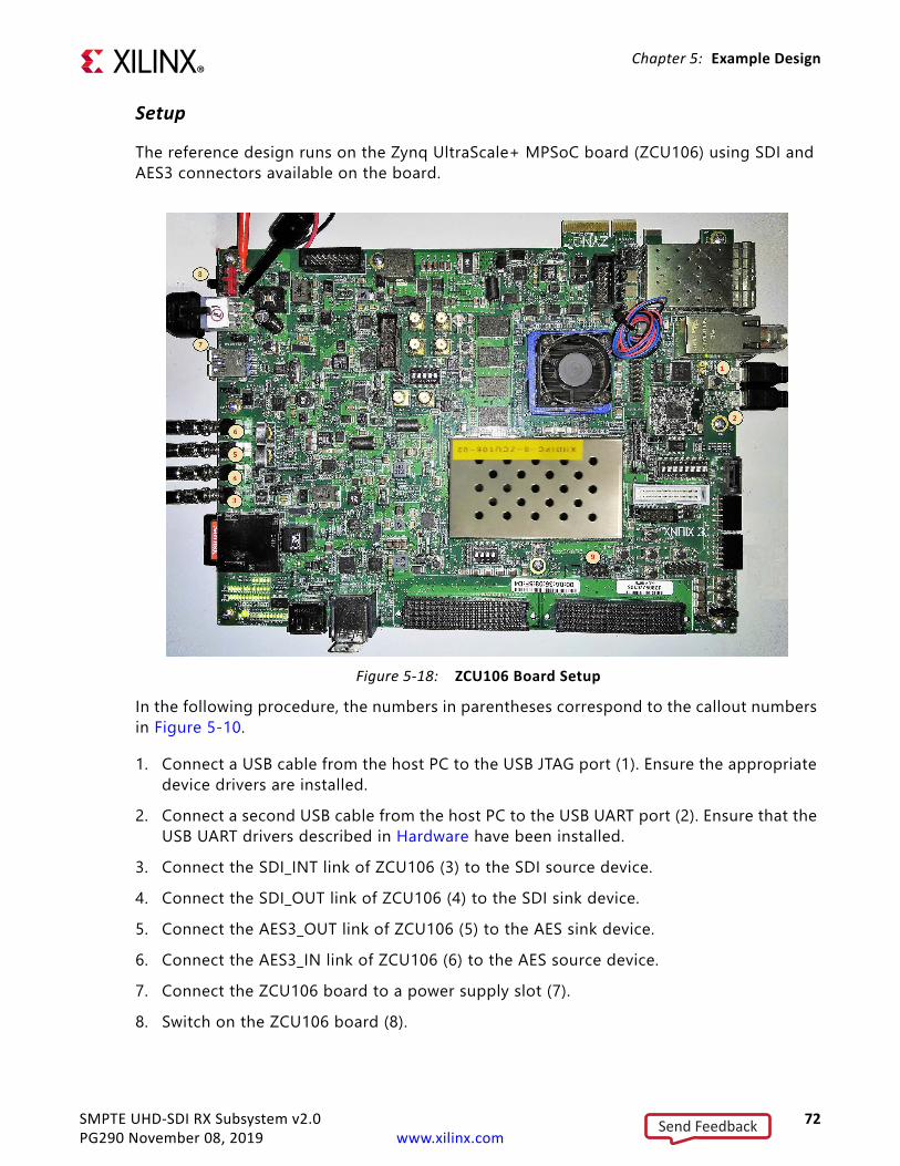
SMPTE UHD-SDI RX Subsystem v2.0 72PG290 November 08, 2019 www.xilinx.com
Chapter 5: Example Design
Setup
The reference design runs on the Zynq UltraScale+ MPSoC board (ZCU106) using SDI and AES3 connectors available on the board.
In the following procedure, the numbers in parentheses correspond to the callout numbers in Figure 5-10.
1. Connect a USB cable from the host PC to the USB JTAG port (1). Ensure the appropriate device drivers are installed.
2. Connect a second USB cable from the host PC to the USB UART port (2). Ensure that the USB UART drivers described in Hardware have been installed.
3. Connect the SDI_INT link of ZCU106 (3) to the SDI source device.4. Connect the SDI_OUT link of ZCU106 (4) to the SDI sink device.5. Connect the AES3_OUT link of ZCU106 (5) to the AES sink device. 6. Connect the AES3_IN link of ZCU106 (6) to the AES source device.7. Connect the ZCU106 board to a power supply slot (7).8. Switch on the ZCU106 board (8).
X-Ref Target - Figure 5-18
Figure 5-18: ZCU106 Board Setup
Send Feedback

SMPTE UHD-SDI RX Subsystem v2.0 73PG290 November 08, 2019 www.xilinx.com
Chapter 5: Example Design
9. Make sure that the HW-ZCU106 board revision (9) is Rev C.10. Ensure that the SMPTE ST 352/Payload ID is enabled in the SDI Stream connected to the
SDI input link of ZCU106.11. Start Tera Term or PuTTY to connect to the COM port interface 0 on the Host PC
configured with 115200 bps, 8 bits, No parity, 1 stop bit, and no flow control.
Compiling Software in Vitis Software PlatformThe UHD-SDI application example design generates a .elf file automatically. Use the following procedure if you want to open the Vitis software platform project for UHD-SDI example design from the Vivado Design Suite:
1. In the Vivado Design Suite, click Tools > Launch Vitis.2. Select Exported location and workspace as <Proj Dir>/SW/xsdi_app and click OK
to launch and open the Vitis software platform project.
Vitis software platform project opens.
Running the Design on the HardwareThe following steps are used to run the BIT and ELF files on the hardware setup:
1. Connect the JTAG cable and USB-UART cable to the board.2. Navigate to <Component Name>_ex/imports.3. Start the Xilinx Software Debugger (XSDB) by sourcing XSDB from the build area from
the command prompt.4. Run the following command to program FPGA and to execute the application.
source xsdb.tcl
5. To observe the results, open Tera Term or PUTTY and configure its serial port (Interface 0) to 115200 baud with the default configuration. Make sure that the UART cable is connected to the board and the PC.
The UART console displays SDI stream details on console.
Send Feedback

SMPTE UHD-SDI RX Subsystem v2.0 74PG290 November 08, 2019 www.xilinx.com
Chapter 5: Example Design
UART Console ScreensThe following figure shows the initial UART console output along with menu options.X-Ref Target - Figure 5-19
Figure 5-19: UART Console - UHD SDI Example Design UART Menu
Send Feedback

SMPTE UHD-SDI RX Subsystem v2.0 75PG290 November 08, 2019 www.xilinx.com
Chapter 5: Example Design
The following figure shows the UART console output when the i key is pressed.X-Ref Target - Figure 5-20
Figure 5-20: UART Console - Receive and Transmit UHD SDI Stream Information
Send Feedback

SMPTE UHD-SDI RX Subsystem v2.0 76PG290 November 08, 2019 www.xilinx.com
Chapter 5: Example Design
KCU116 SMPTE UHD-SDI Audio-Video Loopback Example DesignThe UHD-SDI audio-video loopback example design is built using the UHD-SDI TX and RX subsystems along with the UHD-SDI Audio IP core. Video data generated by the video test pattern generator is passed to the UHD-SDI TX Subsystem. The UHD-SDI TX Subsystem outputs SDI stream after insertion of the ST352 payload (if any) and passed to the UHD-SDI Audio (Embed) IP for audio data insertion. To do so, bit 18 (use_anc_in) of sdi_tx_ctrl[31:0] has to be set to 1’b1 in the UHD-SDI TX Subsystem. Audio data is generated by the audio test pattern generator. See Appendix D to for more information on the audio test pattern generator. Native SDI video stream with audio insertion is passed to the UHD-SDI TX IP for transmission. The UHD-SDI RX Subsystem receives video and audio and passes the native video stream to the UHD-SDI Audio (Extract) IP. Audio is extracted by UHD-SDI Audio IP. The UHD-SDI TX Subsystem, UHD-SDI RX Subsystem, UHD-SDI Audio (Embed) IP, and UHD-SDI Audio (Extract) IP are configured through ports and does not include the AXI4-Lite interface for this example design. The example design application software runs on a MicroBlaze™ processor.
Note: The MicroBlaze processor is not shown in the above figure for simplicity.
X-Ref Target - Figure 5-21
Figure 5-21: KCU116 Audio-Video Loopback Example DesignX21412-090618
Send Feedback

SMPTE UHD-SDI RX Subsystem v2.0 77PG290 November 08, 2019 www.xilinx.com
Chapter 5: Example Design
ClockingThe KCU116 UHD-SDI loopback example design GT clocking architecture is shown in the following figure.
Two reference clocks are used to support integer and fractional line rates of SDI. The reference clock for QPLL0 is fixed to 297 MHz from the on-board Si570 chip. The reference clock for CPLL is fixed at 296.7 MHz from Si5328 chip output. CPLL switches between 297 MHz and 296.7 MHz reference clocks using the CPLLREFCLKSEL.
When using QPLL0 and QPLL1 for 12G-SDI integer and fractional (1/1.001) rate change, switching between rates on the SDI-RX can introduce a glitch on the clock which in turn introduces CRC errors on the TX channel. CRC errors do not occur in SD-SDI/HD-SDI/3-G SDI/6-G SDI integer/fractional modes with QPLL0 and QPLL1 clocking combination. For more information, see Answer Record 72254 and 72449. Therefore, it is not recommended to use this clocking configuration when both transmit and receive 12G-SDI integer and fractional modes use the same transceiver. If required, Xilinx recommends to use CPLL-QPLL combination with CPLL for TX and QPLL0/1 for RX as shown in Figure 5-22. The integer and fractional rates for TX can be selected using CPLL reference clock input selection with 297 MHz and 296.7 MHz respectively. This CPLL/QPLL clocking combination is not feasible with -1 speed grade devices since CPLL does not support 12G-SDI line rates. You need to select an UltraScale+ GTH/GTY -2 speed grade or faster rate with >0.85V. Refer the respective FPGA device data sheets for CPLL line rate limits. The UHD-SDI example designs are updated to use the CPLL and QPLL clocking combination. The UHD-SDI GT IP is updated to provide CPLL support starting from 2019.2.
Running the KCU116 Audio-Video Loopback Example Design1. Open the Vivado Design Suite and create a new project.2. In the pop-up window, press Next 5 times.
X-Ref Target - Figure 5-22
Figure 5-22: Loopback Example Design GT Clocking Architecture
RX
TX
QPLL0
QPLL1
IBUFGDS_GT
IBUFGDS_GT CPLL
GTYE4_CHANNELRXPLLCLKSEL
297 MHZ
296.7 MHZ
CPLLREFCLKSEL X23053-072919
Send Feedback

SMPTE UHD-SDI RX Subsystem v2.0 78PG290 November 08, 2019 www.xilinx.com
Chapter 5: Example Design
3. Select the KCU116 Board.
4. Click Finish.5. Click IP Catalog and double-click SMPTE UHD-SDI RX Subsystem under Video
Connectivity.
Send Feedback
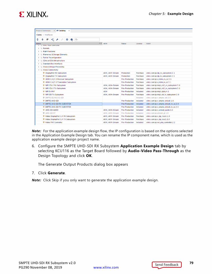
SMPTE UHD-SDI RX Subsystem v2.0 79PG290 November 08, 2019 www.xilinx.com
Chapter 5: Example Design
Note: For the application example design flow, the IP configuration is based on the options selected in the Application Example Design tab. You can rename the IP component name, which is used as the application example design project name.6. Configure the SMPTE UHD-SDI RX Subsystem Application Example Design tab by
selecting KCU116 as the Target Board followed by Audio-Video Pass-Through as the Design Topology and click OK.
The Generate Output Products dialog box appears
7. Click Generate.Note: Click Skip if you only want to generate the application example design.
Send Feedback

SMPTE UHD-SDI RX Subsystem v2.0 80PG290 November 08, 2019 www.xilinx.com
Chapter 5: Example Design
8. Right click the SMPTE UHD-SDI RX Subsystem component under Design source, and click Open IP Example Design.
Send Feedback

SMPTE UHD-SDI RX Subsystem v2.0 81PG290 November 08, 2019 www.xilinx.com
Chapter 5: Example Design
9. Choose the target project location and click OK.
The IP integrator design is then generated and creates the Xilinx® Vitis™ software platform and generates a.elf file. You can choose to Run Synthesis, Implementation, or Generate Bitstream. An overall system IP integrator block diagram of the KCU116-based application example design is shown here.
Requirements
Hardware
The hardware requirements for this reference system are:
• Xilinx Kintex UltraScale+ FPGA KCU116 Evaluation Kit• Fidus TB-FMCH-12GSDI SDI FMC card• One HD-BNC to HD-BNC cable
X-Ref Target - Figure 5-23
Figure 5-23: IP Integrator Diagram of the KCU116 Audio-Video Loopback Example Design
Send Feedback

SMPTE UHD-SDI RX Subsystem v2.0 82PG290 November 08, 2019 www.xilinx.com
Chapter 5: Example Design
Software
This section lists the software requirements:
• Vivado Design Suite 2019.2 or later• The Vitis software platform 2019.2• Software terminals (for example, Tera Term, HyperTerminal or PuTTY)
Setup
This example runs on KCU116 board and more information about the board can be found on the product page.
In the following procedure, the numbers in parentheses correspond to the call out numbers in Figure 5-24.
1. Connect a USB cable from the host PC to the USB JTAG port (1). Ensure the appropriate device drivers are installed.
2. Connect a second USB cable from the host PC to the USB UART port (2). Ensure that the USB UART drivers described in Hardware have been installed.
3. Insert Fidus FMC card into FMC slot (3).
X-Ref Target - Figure 5-24
Figure 5-24: KCU116 Board Setup
Send Feedback

SMPTE UHD-SDI RX Subsystem v2.0 83PG290 November 08, 2019 www.xilinx.com
Chapter 5: Example Design
4. Connect the HD-BNC to HD-BNC cable (4) in Fidus FMC5. Connect the KCU116 board to a power supply slot (5).6. Switch on the KCU116 board (6).7. Make sure that the HW-KCU116 board revision (7) is Rev B.8. Start Tera Term or PuTTY to connect to the COM port interface 0 on the Host PC with
115200 bps, 8 bits, No parity, 1 stop bit, and no flow control as configuration.9. Verify the FMC_VADJ voltage to 1.8V.
Compiling Software in the Vitis Software PlatformThe UHD-SDI application example design generates a .elf file automatically. Follow the steps if you want to open the Vitis software platform project for the UHD-SDI example design from the Vivado Design Suite:
1. In the Vivado Design Suite, click Tools > Launch Vitis.2. Select Exported location and workspace as <Proj Dir>/SW/xsdi_app and click OK
to launch and open the Vitis software platform project.
The Vitis software platform project is now open.
Running the design on the hardwareThe following steps are used to run the BIT and ELF files on the hardware setup:
1. Connect the JTAG cable and USB-UART cable to the board.2. Go to <Component Name>_ex/imports.3. Start the Xilinx Software Debugger (XSDB) by sourcing xsdb from the build area to the
command prompt.4. Run the following command, source xsdb.tcl, to program FPGA and to execute the
application.5. To observe the results, open Tera Term or PUTTY, and configure the serial port (Interface
0) to 115200 baud with the default configuration. Note: Make sure that the UART cable is connected to the board and the PC.
The UART console now displays the SDI stream details on the console.
Send Feedback
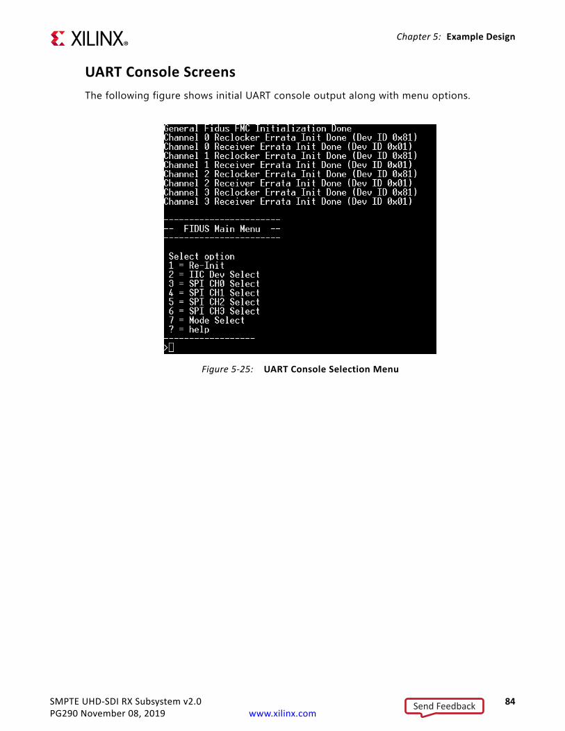
SMPTE UHD-SDI RX Subsystem v2.0 84PG290 November 08, 2019 www.xilinx.com
Chapter 5: Example Design
UART Console ScreensThe following figure shows initial UART console output along with menu options.X-Ref Target - Figure 5-25
Figure 5-25: UART Console Selection Menu
Send Feedback
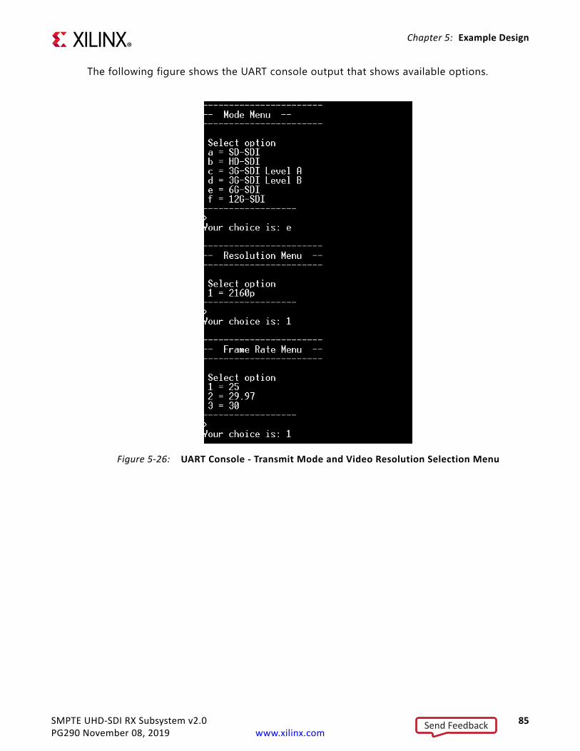
SMPTE UHD-SDI RX Subsystem v2.0 85PG290 November 08, 2019 www.xilinx.com
Chapter 5: Example Design
The following figure shows the UART console output that shows available options.X-Ref Target - Figure 5-26
Figure 5-26: UART Console - Transmit Mode and Video Resolution Selection Menu
Send Feedback

SMPTE UHD-SDI RX Subsystem v2.0 86PG290 November 08, 2019 www.xilinx.com
Chapter 5: Example Design
The following figure shows the UART console output that shows test pass indication.X-Ref Target - Figure 5-27
Figure 5-27: UART Console: Shows Received UHD SDI Mode Matehces with Transmitted UHD SDI Mode
Send Feedback
SMPTE UHD-SDI RX Subsystem v2.0 87PG290 November 08, 2019 www.xilinx.com
Appendix A
Verification, Compliance, and Interoperability
The SMPTE UHD-SDI RX Subsystem has been verified using both simulation and hardware testing.
A highly parameterizable transaction-based simulation test suite has been used to verify the subsystem. The tests include:
• Different SDI standard.• Different resolutions with different video timing parameters.• Recovery from error conditions.• Register read and write access.
InteroperabilityThe SMPTE UHD-SDI RX Subsystem has been tested using standard off-the-shelf SDI test equipment with a variety of UHD-SDI devices. It is compliant with the SMPTE SDI standards.
Send Feedback

SMPTE UHD-SDI RX Subsystem v2.0 88PG290 November 08, 2019 www.xilinx.com
Appendix A: Verification, Compliance, and Interoperability
Hardware ValidationThe SMPTE UHD-SDI RX Subsystem is tested in hardware for functionality, performance, and reliability using Xilinx® evaluation platforms. The SMPTE UHD-SDI RX Subsystem verification test suites for all possible modules are continuously being updated to increase test coverage across the range of possible parameters for each individual module.
The SMPTE UHD-SDI RX Subsystem has been validated using
• Zynq® UltraScale+™ MPSoC ZCU106 Evaluation Kit• Kintex® UltraScale+ KCU116 Evaluation Kit
The SMPTE UHD-SDI RX Subsystem is tested with following devices:
• Phabrix QX 12G as Source and Sync device• Phabrix R1000 as Source and Sync device• Phabrix SX as Source and Sync device• Omnitek Ultra 4K Tool box as Source and Sync deviceTable A-1: Tested Configurations
Board PLL Source Sink Type Model Number Sink Firmware Status
ZCU106 (GTH)
QPLL0/QPLL1Phabrix QX ver 3.0 PassOmnitek Ultra 4K ver 4.0.74.0 Pass
Black Magic Teranex Mini NA Pass
CPLLPhabrix QX ver 3.0 PassOmnitek Ultra 4K ver 4.0.74.0 Pass
Black Magic Teranex Mini NA Pass
KCU116 (GTY)
QPLL0/QPLL1Phabrix QX ver 3.0 PassOmnitek Ultra 4K ver 4.0.74.0 Pass
Black Magic Teranex Mini NA Pass
CPLLPhabrix QX ver 3.0 PassOmnitek Ultra 4K ver 4.0.74.0 Pass
Black Magic Teranex Mini NA Pass
Send Feedback

SMPTE UHD-SDI RX Subsystem v2.0 89PG290 November 08, 2019 www.xilinx.com
Appendix A: Verification, Compliance, and Interoperability
Video ResolutionsA series of interoperability test scenarios, listed in Table A-2 to Table A-4, are validated for different resolutions. Test equipment is used to drive the SDI mode specific traffic and display the received SDI data. Figure A-1 shows the UHD-SDI validation setup using SDI Test equipment.
Table A-2 shows the tested video resolutions using the Phabrix QX 12G as the SDI source and SDI sink.
X-Ref Target - Figure A-1
Figure A-1: SMPTE UHD-SDI Test Equipment Setup X21457-090618
Send Feedback

SMPTE UHD-SDI RX Subsystem v2.0 90PG290 November 08, 2019 www.xilinx.com
Appendix A: Verification, Compliance, and Interoperability
Table A-2: Tested Video Resolutions for YCbCr 4:2:2 at 10 Bits/Component
SDI Mode ResolutionHorizontal Vertical Frame
Rate(Hz)Total Active Total Active
HD-SDI
1920x1080i50 2640 1920 1125 1080 501920x1080i59.94 2200 1920 1125 1080 59.94
1920x1080i60 2200 1920 1125 1080 601280x720p25 3960 1280 750 720 25
1280x720p29.97 3300 1280 750 720 29.971280x720p30 3300 1280 750 720 301280x720p50 1980 1280 750 720 50
1280x720p59.94 1650 1280 750 720 59.941280x720p60 1650 1280 750 720 60
1920x1080p23.98 2750 1920 1125 1080 23.981920x1080p24 2750 1920 1125 1080 241920x1080p25 2640 1920 1125 1080 25
1920x1080p29.97 2200 1920 1125 1080 29.971920x1080p30 2200 1920 1125 1080 30
3G-SDI Level A1920x1080p50 2640 1920 1125 1080 50
1920x1080p59.94 2200 1920 1125 1080 59.941920x1080p60 2200 1920 1125 1080 60
HD-SDI
2048x1080p23.98 2750 2048 1125 1080 23.982048x1080p24 2750 2048 1125 1080 242048x1080p25 2640 2048 1125 1080 25
2048x1080p29.97 2200 2048 1125 1080 29.972048x1080p30 2200 2048 1125 1080 30
3G-SDI Level A, 3G-SDI Level B
2048x1080p47.95 2750 2048 1125 1080 47.952048x1080p48 2750 2048 1125 1080 482048x1080p50 2640 2048 1125 1080 50
2048x1080p59.94 2200 2048 1125 1080 59.942048x1080p60 2200 2048 1125 1080 60
6G-SDI
3840x2160p23.98 5500 3840 2250 2160 23.983840x2160p24 5500 3840 2250 2160 243840x2160p25 5280 3840 2250 2160 25
3840x2160p29.97 4400 3840 2250 2160 29.973840x2160p30 4400 3840 2250 2160 30
Send Feedback

SMPTE UHD-SDI RX Subsystem v2.0 91PG290 November 08, 2019 www.xilinx.com
Appendix A: Verification, Compliance, and Interoperability
Table A-3 shows the tested video resolutions using the Phabrix R1000/Phabrix SX as the SDI source and SDI sink.
12G-SDI3840x2160p50 5280 3840 2250 2160 50
3840x2160p59.94 4400 3840 2250 2160 59.943840x2160p60 4400 3840 2250 2160 60
6G-SDI
4096x2160p23.98 5500 4096 2200 2160 23.984096x2160p24 5500 4096 2200 2160 244096x2160p25 5280 4096 2250 2160 25
4096x2160p29.97 4400 4096 2250 2160 29.974096x2160p30 4400 4096 2250 2160 30
12G-SDI
4096x2160p47.95 5500 4096 2250 2160 47.954096x2160p48 5500 4096 2250 2160 484096x2160p50 5280 4096 2250 2160 50
4096x2160p59.94 4400 4096 2250 2160 59.944096x2160p60 4400 4096 2250 2160 60
Table A-3: Tested Video Resolutions for YCbCr 4:2:2 at 10 Bits/Component
SDI Mode ResolutionHorizontal Vertical Frame
Rate(Hz)Total Active Total Active
SD-SDI 625i50 864 720 625 576 50
HD-SDI
1920x1080sF23.98 2750 1920 1125 1080 23.981920x1080sF24 2750 1920 1125 1080 23.981920x1080sF25 2640 1920 1125 1080 23.98
1920x1080sF29.97 2200 1920 1125 1080 29.971920x1080sF30 2200 1920 1125 1080 30
3G-SDI Level A,3G-SDI Level B
1920x1080p47.95 2750 1920 1125 1080 47.951920x1080p48 2750 1920 1125 1080 48
Table A-2: Tested Video Resolutions for YCbCr 4:2:2 at 10 Bits/Component (Cont’d)
SDI Mode ResolutionHorizontal Vertical Frame
Rate(Hz)Total Active Total Active
Send Feedback

SMPTE UHD-SDI RX Subsystem v2.0 92PG290 November 08, 2019 www.xilinx.com
Appendix A: Verification, Compliance, and Interoperability
Table A-4 shows the tested video resolutions using the Omnitek Ultra 4K Tool box as the SDI source and SDI sink.
Table A-4: Tested Video Resolutions for YCbCr 4:2:2 at 10 Bits/Component
SDI Mode ResolutionHorizontal Vertical Frame
Rate(Hz)Total Active Total Active
SD-HDI 720x576i50 - 720 - 576 50
HD-SDI
1920x1080i47.95 - 1920 - 1080 47.951920x1080i48 - 1920 - 1080 481920x1080i50 - 1920 - 1080 50
1920x1080i59.94 - 1920 - 1080 59.941920x1080i60 - 1920 - 1080 60
2048x1080i47.95 - 2048 - 1080 47.952048x1080i48 - 2048 - 1080 482048x1080i50 - 2048 - 1080 50
2048x1080i59.94 - 2048 - 1080 59.942048x1080i60 - 2048 - 1080 601280x720p25 - 1280 - 720 25
1280x720p29.97 - 1280 - 720 29.971280x720p30 - 1280 - 720 301280x720p50 - 1280 - 720 50
1280x720p59.94 - 1280 - 720 59.941280x720p60 - 1280 - 720 60
1920x1080p23.98 - 1920 - 1080 23.981920x1080p24 - 1920 - 1080 241920x1080p25 - 1920 - 1080 25
1920x1080p29.97 - 1920 - 1080 29.971920x1080p30 - 1920 - 1080 30
1920x1080sF23.98 - 1920 - 1080 23.981920x1080sF24 - 1920 - 1080 241920x1080sF25 - 1920 - 1080 25
1920x1080sF29.97 - 1920 - 1080 29.971920x1080sF30 - 1920 - 1080 30
2048x1080p23.98 - 2048 - 1080 23.982048x1080p24 - 2048 - 1080 242048x1080p25 - 2048 - 1080 25
2048x1080p29.97 - 2048 - 1080 29.97
Send Feedback

SMPTE UHD-SDI RX Subsystem v2.0 93PG290 November 08, 2019 www.xilinx.com
Appendix A: Verification, Compliance, and Interoperability
HD-SDI
2048x1080p30 - 2048 - 1080 302048x1080sF23.98 - 2048 - 1080 23.98
2048x1080sF24 - 2048 - 1080 242048x1080sF25 - 2048 - 1080 25
2048x1080sF29.97 - 2048 - 1080 29.972048x1080sF30 - 2048 - 1080 30
3G-A
1920x1080p47.95 - 1920 - 1080 47.951920x1080p48 - 1920 - 1080 481920x1080p50 - 1920 - 1080 50
1920x1080p59.94 - 1920 - 1080 59.941920x1080p60 - 1920 - 1080 60
2048x1080p47.95 - 2048 - 1080 47.952048x1080p48 - 2048 - 1080 482048x1080p50 - 2048 - 1080 50
2048x1080p59.94 - 2048 - 1080 59.942048x1080p60 - 2048 - 1080 60
3G-B DL
1920x1080p47.95 - 1920 - 1080 47.951920x1080p48 - 1920 - 1080 481920x1080p50 - 1920 - 1080 50
1920x1080p59.94 - 1920 - 1080 59.941920x1080p60 - 1920 - 1080 60
2048x1080p47.95 - 2048 - 1080 47.952048x1080p48 - 2048 - 1080 482048x1080p50 - 2048 - 1080 50
2048x1080p59.94 - 2048 - 1080 59.942048x1080p60 - 2048 - 1080 60
3G-B DS
1920x1080i47.95 - 1920 - 1080 47.951920x1080i48 - 1920 - 1080 481920x1080i50 - 1920 - 1080 50
1920x1080i59.94 - 1920 - 1080 59.941920x1080i60 - 1920 - 1080 60
2048x1080i47.95 - 2048 - 1080 47.952048x1080i48 - 2048 - 1080 48
Table A-4: Tested Video Resolutions for YCbCr 4:2:2 at 10 Bits/Component (Cont’d)
SDI Mode ResolutionHorizontal Vertical Frame
Rate(Hz)Total Active Total Active
Send Feedback

SMPTE UHD-SDI RX Subsystem v2.0 94PG290 November 08, 2019 www.xilinx.com
Appendix A: Verification, Compliance, and Interoperability
3G-B DS
2048x1080i50 - 2048 - 1080 502048x1080i59.94 - 2048 - 1080 59.94
2048x1080i60 - 2048 - 1080 601920x1080sF23.98 - 1920 - 1080 23.98
1920x1080sF24 - 1920 - 1080 241920x1080sF25 - 1920 - 1080 25
1920x1080sF29.97 - 1920 - 1080 29.971920x1080sF30 - 1920 - 1080 30
2048x1080sF23.98 - 2048 - 1080 23.982048x1080sF24 - 2048 - 1080 242048x1080sF25 - 2048 - 1080 25
2048x1080sF29.97 - 2048 - 1080 29.972048x1080sF30 - 2048 - 1080 30
6G-SDI
3840x2160p23.98 - 3840 - 2160 23.983840x2160p24 - 3840 - 2160 243840x2160p25 - 3840 - 2160 25
3840x2160p29.97 - 3840 - 2160 29.973840x2160p30 - 3840 - 2160 30
4096x2160p23.98 - 4096 - 2160 23.984096x2160p24 - 4096 - 2160 244096x2160p25 - 4096 - 2160 25
4096x2160p29.97 - 4096 - 2160 29.974096x2160p30 - 4096 - 2160 30
12G-SDI
3840x2160p47.95 - 3840 - 2160 47.953840x2160p48 - 3840 - 2160 483840x2160p50 - 3840 - 2160 50
3840x2160p59.94 - 3840 - 2160 59.943840x2160p60 - 3840 - 2160 60
4096x2160p47.95 - 4096 - 2160 47.954096x2160p48 - 4096 - 2160 484096x2160p50 - 4096 - 2160 50
4096x2160p59.94 - 4096 - 2160 59.944096x2160p60 - 4096 - 2160 60
Table A-4: Tested Video Resolutions for YCbCr 4:2:2 at 10 Bits/Component (Cont’d)
SDI Mode ResolutionHorizontal Vertical Frame
Rate(Hz)Total Active Total Active
Send Feedback

SMPTE UHD-SDI RX Subsystem v2.0 95PG290 November 08, 2019 www.xilinx.com
Appendix A: Verification, Compliance, and Interoperability
Table A-5 shows tested video resolutions for YCbCr 4:4:4 at 10 Bits/Component.
Table A-5: Tested Video Resolutions for YCbCr 4:4:4 at 10 Bits/Component
SDI Mode Video ResolutionHorizontal Vertical
Scan Type/Frame RateActive Active
12G 3840x2160 3840 2160 p23.9812G 3840x2160 3840 2160 p2412G 3840x2160 3840 2160 p2512G 3840x2160 3840 2160 p29.9712G 3840x2160 3840 2160 p3012G 4096x2160 4096 2160 p23.9812G 4096x2160 4096 2160 p2412G 4096x2160 4096 2160 p2512G 4096x2160 4096 2160 p29.9712G 4096x2160 4096 2160 p30
3G B-DL 1920x1080 1920 1080 p23.983G B-DL 1920x1080 1920 1080 p243G B-DL 1920x1080 1920 1080 p253G B-DL 1920x1080 1920 1080 p29.973G B-DL 1920x1080 1920 1080 p303G B-DL 1920x1080 1920 1080 SF23.983G B-DL 1920x1080 1920 1080 SF243G B-DL 1920x1080 1920 1080 SF253G B-DL 1920x1080 1920 1080 SF29.973G B-DL 1920x1080 1920 1080 SF303G B-DL 1920x1080 1920 1080 i47.953G B-DL 1920x1080 1920 1080 i483G B-DL 1920x1080 1920 1080 i503G B-DL 1920x1080 1920 1080 i59.943G B-DL 1920x1080 1920 1080 i603G B-DL 2048x1080 2048 1080 p23.983G B-DL 2048x1080 2048 1080 p243G B-DL 2048x1080 2048 1080 p253G B-DL 2048x1080 2048 1080 p29.973G B-DL 2048x1080 2048 1080 p303G B-DL 2048x1080 2048 1080 SF23.983G B-DL 2048x1080 2048 1080 SF24
Send Feedback

SMPTE UHD-SDI RX Subsystem v2.0 96PG290 November 08, 2019 www.xilinx.com
Appendix A: Verification, Compliance, and Interoperability
3G B-DL 2048x1080 2048 1080 SF253G B-DL 2048x1080 2048 1080 SF29.973G B-DL 2048x1080 2048 1080 SF303G B-DL 2048x1080 2048 1080 i47.953G B-DL 2048x1080 2048 1080 i483G B-DL 2048x1080 2048 1080 i503G B-DL 2048x1080 2048 1080 i59.943G B-DL 2048x1080 2048 1080 i60
3G A 1280x720 1280 720 p253G A 1280x720 1280 720 p29.973G A 1280x720 1280 720 p303G A 1280x720 1280 720 p503G A 1280x720 1280 720 p59.943G A 1280x720 1280 720 p603G A 1280x720 1280 720 p603G A 1920x1080 1920 1080 sF23.983G A 1920x1080 1920 1080 sF243G A 1920x1080 1920 1080 sF253G A 1920x1080 1920 1080 sF29.973G A 1920x1080 1920 1080 sF303G A 1920x1080 1920 1080 p23.983G A 1920x1080 1920 1080 p243G A 1920x1080 1920 1080 p253G A 1920x1080 1920 1080 p29.973G A 1920x1080 1920 1080 p303G A 1920x1080 1920 1080 i47.953G A 1920x1080 1920 1080 i483G A 1920x1080 1920 1080 i503G A 1920x1080 1920 1080 i59.943G A 1920x1080 1920 1080 i603G A 2048x1080 2048 1080 p23.983G A 2048x1080 2048 1080 p243G A 2048x1080 2048 1080 p253G A 2048x1080 2048 1080 p29.97
Table A-5: Tested Video Resolutions for YCbCr 4:4:4 at 10 Bits/Component
SDI Mode Video ResolutionHorizontal Vertical
Scan Type/Frame RateActive Active
Send Feedback
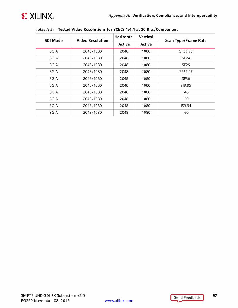
SMPTE UHD-SDI RX Subsystem v2.0 97PG290 November 08, 2019 www.xilinx.com
Appendix A: Verification, Compliance, and Interoperability
3G A 2048x1080 2048 1080 SF23.983G A 2048x1080 2048 1080 SF243G A 2048x1080 2048 1080 SF253G A 2048x1080 2048 1080 SF29.973G A 2048x1080 2048 1080 SF303G A 2048x1080 2048 1080 i49.953G A 2048x1080 2048 1080 i483G A 2048x1080 2048 1080 i503G A 2048x1080 2048 1080 i59.943G A 2048x1080 2048 1080 i60
Table A-5: Tested Video Resolutions for YCbCr 4:4:4 at 10 Bits/Component
SDI Mode Video ResolutionHorizontal Vertical
Scan Type/Frame RateActive Active
Send Feedback

SMPTE UHD-SDI RX Subsystem v2.0 98PG290 November 08, 2019 www.xilinx.com
Appendix B
DebuggingThis appendix includes details about resources available on the Xilinx Support website and debugging tools.
Finding Help on Xilinx.comTo help in the design and debug process when using the SMPTE UHD-SDI RX, the Xilinx Support web page (www.xilinx.com/support) contains key resources such as product documentation, release notes, answer records, information about known issues, and links for obtaining further product support.
DocumentationThis product guide is the main document associated with the SMPTE UHD-SDI RX. This guide, along with documentation related to all products that aid in the design process, can be found on the Xilinx Support web page (www.xilinx.com/support) or by using the Xilinx Documentation Navigator.
Download the Xilinx Documentation Navigator from the Design Tools tab on the Downloads page (www.xilinx.com/download). For more information about this tool and the features available, open the online help after installation.
Solution CentersSee the Xilinx Solution Centers for support on devices, software tools, and intellectual property at all stages of the design cycle. Topics include design assistance, advisories, and troubleshooting tips.
The Solution Center specific to the SMPTE UHD-SDI RX core is listed below.
• Xilinx Video Solution Center
Answer Records Answer Records include information about commonly encountered problems, helpful information on how to resolve these problems, and any known issues with a Xilinx product.
Send Feedback
SMPTE UHD-SDI RX Subsystem v2.0 99PG290 November 08, 2019 www.xilinx.com
Appendix B: Debugging
Answer Records are created and maintained daily ensuring that users have access to the most accurate information available.
Answer Records for this core can be located by using the Search Support box on the main Xilinx support web page. To maximize your search results, use proper keywords such as
• Product name• Tool message(s)• Summary of the issue encountered
A filter search is available after results are returned to further target the results.
Master Answer Record for the SMPTE UHD-SDI RX
AR: 68766
Technical SupportXilinx provides technical support at the Xilinx Support web page for this LogiCORE™ IP product when used as described in the product documentation. Xilinx cannot guarantee timing, functionality, or support if you do any of the following:
• Implement the solution in devices that are not defined in the documentation.• Customize the solution beyond that allowed in the product documentation. • Change any section of the design labeled DO NOT MODIFY.
To contact Xilinx Technical Support, navigate to the Xilinx Support web page.
Debug ToolsThere are many tools available to address SMPTE UHD-SDI RX design issues. It is important to know which tools are useful for debugging various situations.
Send Feedback
SMPTE UHD-SDI RX Subsystem v2.0 100PG290 November 08, 2019 www.xilinx.com
Appendix B: Debugging
Vivado Lab EditionVivado® Lab Edition inserts logic analyzer and virtual I/O cores directly into your design. Vivado Lab Edition also allows you to set trigger conditions to capture application and integrated block port signals in hardware. Captured signals can then be analyzed. This feature in the Vivado IDE is used for logic debugging and validation of a design running in Xilinx.
The Vivado logic analyzer is used with the logic debug IP cores, including:
• ILA 2.0 (and later versions)• VIO 2.0 (and later versions)
See the Vivado Design Suite User Guide: Programming and Debugging (UG908) [Ref 6].
Hardware DebugHardware issues can range from link bring-up to problems seen after hours of testing. This section provides debug steps for common issues. The Vivado debug feature is a valuable resource to use in hardware debug. The signal names mentioned in the following individual sections can be probed using the debug feature for debugging the specific problems.
General ChecksEnsure that all the timing constraints for the core were properly incorporated from the example design and that all constraints were met during implementation.
• Check that MMCM lock and PLL lock signal(s) are asserted.• Verify the IO pin planning and XDC constraints.• Follow the recommended reset sequence.• Verify all clocks are connected and are with expected frequencies.• Enable AXI4 Lite based register interface to get core status and control.• Make sure serial line trace lengths are equal.• Verify the FMC_VADJ voltage to 1.8V in case of FMC card usage.
Send Feedback

SMPTE UHD-SDI RX Subsystem v2.0 101PG290 November 08, 2019 www.xilinx.com
Appendix B: Debugging
Figure B-1 shows the steps to perform a hardware debug.
GT Clocking
• Make sure QPLL is getting reset before starting the IP.• Monitor the QPLL LOCK signal.• Verify that QPLL input clock frequency is of expected value.• It is mandatory to reset the QPLL if clock input to QPLL is stopped or unstable.• See AR#57738 for debugging GT reference clock issues.• Make sure to use QPLL default settings from latest GT Wizard IP core based on target
device.• Check the voltage rails on the transceivers. See AR#57737 for more information.• Measure RXOUTCLK is of expected frequency.
X-Ref Target - Figure B-1
Figure B-1: Hardware DebuggingX21887-111218
Send Feedback

SMPTE UHD-SDI RX Subsystem v2.0 102PG290 November 08, 2019 www.xilinx.com
Appendix B: Debugging
• Make sure RXOUTCLK of the transceiver is the clock driving rx_usrclk, RXUSRCLK, and RXUSRCLK2.
• Monitor RXBUFFSTATUS[2:0] for overflow and underflow errors.
GT Initialization
• GTRXRESETDONE is asserted High after GT completes initialization.• Make sure GT is not reset during normal operation.• See AR#59435 for more information on debugging GT reset problems.• Follow the recommended GT reset sequence.
SDI Mode Detection
• The UHD-SDI RX core hunts for TRS symbols and asserts rx_mode_locked if the UHD-SDI core detects error-free TRS symbols (that is, a valid XYZ word and with no CRC errors on the received line) for continuous three video lines.
• Look for pulses on the rx_eav, rx_sav signals at the correct places on each line along with rx_trs signal.
• Make sure no CRC errors are reported on rx_crc_err_ds1 to ds16.• Make sure supported modes are enabled in the rx_mode_enable[5:0] signal.• Verify that rx_mode[2:0] reported by the SDI core matches the incoming SDI mode.• SDI Mode detection searches the mode in the following fashion if all of the modes are
set in rx_mode_enable: HD -> 3G -> 6G -> 12GA -> 12GB -> SD -> HD.• Make sure that rx_frame_en signal is asserted High during core operation.
SDI Transport Detection
• The UHD-SDI core reports the video format by asserting rx_t_locked signal.• This functionality takes two video frames to report the transport format• Check the rx_t_family[3:0], rx_t_rate[3:0], rx_t_scan and rx_t_locked
signals.• Make sure the incoming video format is supported by the UHD-SDI core.• Check that the rx_bit_rate signal is connected to the core.
UHD-SDI RX Data Reception
• UHD-SDI core receives the data in this stage until it receives erroneous video lines or change in incoming video source.
Send Feedback

SMPTE UHD-SDI RX Subsystem v2.0 103PG290 November 08, 2019 www.xilinx.com
Appendix B: Debugging
UHD-SDI Mode Change
• UHD-SDI core deasserts rx_mode_locked signal if it receives 15 or more erroneous video lines continuously.
• After rx_mode_locked is deasserted, it starts the SDI mode scan.
SDI RX to Video Bridge Debug:
• Make sure correct SDI mode (rx_mode[2:0] input) is passed on to SDI RX to Video Bridge subcore.
• Verify first pixel data is data on input native SDI data stream is appearing on native Video interface by monitoring vid_data[59:0] data bus along with other control signals such as vid_active_video, vid_hblank and vid_vblank.
Video In to AXI4-Stream Debug:
• Verify first pixel data is data on input native video interface is appearing on AXI4 Video interface by monitoring m_axis_video_tdata[63:0] data bus along with control signals such as m_axis_video_tvalid and m_axis_video_tready.
• Make sure that underflow and overflow outputs are not asserted. If asserted, verify the clock connections and along with expected frequencies.
Interface DebugAXI4-Lite InterfacesRead from a register that does not have all 0s as a default to verify that the interface is functional. See Figure B-2 and Figure B-3. Output s_axi_arready asserts when the read address is valid, and output s_axi_rvalid asserts when the read data/response is valid. If the interface is unresponsive, ensure that the following conditions are met:
• The s_axi_aclk and aclk inputs are connected and toggling. • The interface is not being held in reset, and s_axi_areset is an active-Low reset.• The interface is enabled, and s_axi_aclken is active-High (if used).• The main core clocks are toggling and that the enables are also asserted. • If the simulation has been run, verify in simulation and/or a debug feature capture that
the waveform is correct for accessing the AXI4-Lite interface.
Send Feedback

SMPTE UHD-SDI RX Subsystem v2.0 104PG290 November 08, 2019 www.xilinx.com
Appendix B: Debugging
X-Ref Target - Figure B-2
Figure B-2: ReadX-Ref Target - Figure B-3
Figure B-3: Write
Send Feedback

SMPTE UHD-SDI RX Subsystem v2.0 105PG290 November 08, 2019 www.xilinx.com
Appendix C
UHD-SDI GT 2.0 IPThis appendix provides information on the UHD-SDI GT IP core that is used in SMPTE UHD-SDI Subsystem example designs and provides details on clocking and use cases.
Using UltraScale+ GTH/GTY Transceivers for SDIThe information in this section is intended to supplement, not replace, the information in the UltraScale Architecture GTH Transceivers User Guide (UG576) [Ref 12] and UltraScale Architecture GTY Transceivers User Guide (UG578) [Ref 13]. This information highlights features and operating requirements of the GTH/GTY transceivers that are of particular importance for UHD-SDI applications.
In the example design, the naming convention used in the UltraScale Architecture GTH Transceivers User Guide (UG576) [Ref 12] and UltraScale Architecture GTY Transceivers User Guide (UG578) [Ref 13] for the GTH/GTY transceiver ports is followed. This convention is to use only the base name of a port. When the UltraScale™ FPGAs Transceiver Wizard is used to create a GTH/GTY wizard module, all input ports names have a suffix of _in and all outputs have a suffix of _out. For example, when a port named txpllclksel is referred to in this document, the actual name of that port in the GTH/GTY wrapper is txpllclksel_in.
There are several clocks required in applications using GTH/GTY transceivers. The SDI protocol, which does not allow for clock correction by stuffing and removing extra data in the data stream, requires careful attention to how these clocks are generated and used in the application. GTH/GTY transceivers require reference clocks to operate. The reference clocks are used by phase-locked loops (PLLs) in the GTH/GTY transceiver quad to generate serial clocks for the receiver and transmitter sections of each transceiver. As described in GTH Transceiver Reference Clocks, the serial bit rate of the GTH/GTY transmitter is an integer multiple of the reference clock frequency it is using. Furthermore, the data rate of the video provided to the input of the SDI transmitter datapath must also exactly match (or be a specific multiple of) the frequency of the reference clock used by the GTH/GTY transmitter. Consequently, you must determine how to generate the transmitter reference clock so that it is frequency-locked exactly with the data rate of the video stream being transmitted.
The GTH/GTY transmitter clocking is handled by the Transmitter User Clocking Network Helper block when enabled during GT IP generation from the UltraScale FPGAs Transceiver
Send Feedback

SMPTE UHD-SDI RX Subsystem v2.0 106PG290 November 08, 2019 www.xilinx.com
Appendix C: UHD-SDI GT 2.0 IP
Wizard. The txusrclk and txusrclk2 output is driven by a BUFG_GT within the helper block and its frequency is exactly equal to the word rate of the data that must enter the txdata port of the GTH/GTY transmitter. The txusrclk and txusrclk2 are generated in the GTH/GTY transmitter by dividing the serial clock from the PLL down to the word rate. See the UltraScale FPGAs Transceivers Wizard (PG182) [Ref 14] for more details on Transmitter User Clocking Network Helper block.
The GTH/GTY receiver reference clock, however, does not need an exact relationship with the bit rate of the incoming SDI signals. This is because the clock and data recovery (CDR) unit in the GTH/GTY receiver can receive bit rates that are up to ±1,250 ppm (≤ 6.6 Gb/s) or ±200 ppm (> 8.0 Gb/s) away from the nominal bit rate as set by the reference clock frequency. This allows the receiver reference clock to be generated by local oscillators that have no exact frequency relationship to the incoming SDI signal. The GTH/GTY receiver generates a recovered clock that is frequency-locked to the incoming SDI bit rate. These clocks are output as rxusrclk and rxusrclk2 ports of the Receiver User Clocking Network Helper Block from the GTH/GTY Wizard IP and are driven by BUFG_GT. As is described in more detail later, rxusrclk and rxusrclk2 are true recovered clocks when receiving all SDI line rates except when receiving SD-SDI signals.
One additional clock is required for SDI applications. This is a free-running, fixed-frequency clock that is used as the clock for the dynamic reconfiguration port (DRP) of the GTH/GTY transceiver. This same clock is also usually supplied to the control module in the SDI wrapper where it is used for timing purposes. The valid frequency range for this clock is stated in the UltraScale FPGAs Transceiver Wizard and normally ranges from 3.125 to 200 MHz. The frequency of this clock does not require any specific relationship relative to other clocks or data rates of the SDI application. This clock must not change frequencies when the SDI mode changes. It must remain running at the same nominal frequency at all times. It also must never stop while the SDI application is active. This clock can be used for all SD interfaces in the device.
The frequency of the rxusrclk and txusrclk depend on the SDI mode and the width of the rxdata and txdata ports of the GTH/GTY transceiver. This relationship is fixed by the architecture of the GTH/GTY transceiver. The RX and the TX both use clock enables to throttle the data stream transfer data rate because, in some cases, the data rate on the data streams is less than the frequency of the clock. Table C-1 shows the relationships between SDI mode, number of active data streams, rxdata/txdata port widths, rxoutclk/txoutclk frequencies, and clock enable cadences. The clock enable cadences are given in number of clocks between assertions of the clock enable over two data word cycles where 1/1 means that the clock enable is asserted every clock cycle, 2/2 indicates assertion every other clock cycle (50% duty cycle), 4/4 indicates assertion every fourth clock cycle (25% duty cycle), and 5/6 indicates that the clock enable alternates between assertion every 5 or 6 clock cycles, to average once every 5.5 clock cycles (one instance of 5 clock cycles between High pulses on the clock enabled followed by one instance of six clock cycles between High pulses on the clock enable, with this pattern repeating).
Send Feedback

SMPTE UHD-SDI RX Subsystem v2.0 107PG290 November 08, 2019 www.xilinx.com
Appendix C: UHD-SDI GT 2.0 IP
GTH Transceiver Reference Clocks
UltraScale+ GTH transceivers are grouped into quads. Each quad contains four GTHE4_CHANNEL transceiver primitives and one GTHE4_COMMON primitive containing two quad PLLs (QPLL0 and QPLL1) as shown in Figure C-1. The clock generated by the QPLL0 and QPLL1 are distributed to all four transceivers in the quad. Each GTHE4_CHANNEL has its own PLL called the Channel PLL (CPLL), which can provide a clock to the RX and TX of that transceiver only. Each RX and TX unit in the quad can be individually configured to use either/both QPLL0 or/and QPLL1 or the CPLL as its clock source. Furthermore, any RX or TX unit can dynamically switch its clock source between QPLL0, QPLL1 and CPLL. This configuration and the dynamic switching capability are particularly useful for SDI applications.
IMPORTANT: The CPLL and QPLL have maximum line rates of 6.25 Gb/s and 16.375 Gb/s, respectively in an UltraScale -1 speed grade part. This means that CPLL can only be used up to 6G-SDI line rate while QPLLs can support up to 12G-SDI for -1 speed grade UltraScale+ GTH transceivers. The CPLL has a maximum line rate of 4.25 Gb/s and therefore it can only support up to 3G-SDI. This is a limitation only for-1 speed grade devices. See GTH Transceiver Switching Characteristics section of Kintex/Virtex UltraScale+ Architecture Data Sheet: DC and AC Switching Characteristics (DS922) [Ref 15] for details when selecting the appropriate device for your application.
Table C-1: Clock Frequencies and Clock Enable Requirements
SDI-Mode Active Data Streams
RX/TXDATA Bit Width RX/TXOUTCLK Frequency Clock Enable
SD-SDI 1 20 148.5 MHz 5/6HD-SDI 2 20 74.25 or 74.25/1.001 MHz 1/13G-SDI A 2 20 148.5 or 148.5/1.001 MHz 1/13G-SDI B 4 20 148.5 or 148.5/1.001 MHz 2/26G-SDI 4 40 148.5 or 148.5/1.001 MHz 1/16G-SDI 8 40 148.5 or 148.5/1.001 MHz 2/212G-SDI 8 40 297 or 297/1.001 MHz 2/212G-SDI 16 40 297 or 297/1.001 MHz 4/4
Send Feedback

SMPTE UHD-SDI RX Subsystem v2.0 108PG290 November 08, 2019 www.xilinx.com
Appendix C: UHD-SDI GT 2.0 IP
Typical UHD-SDI applications require the GTH transceivers to support nine different bit rates:
• 270 Mb/s for SD-SDI• 1.485 Gb/s for HD-SDI• 1.485/1.001 Gb/s for HD-SDI
X-Ref Target - Figure C-1
Figure C-1: UltraScale+ GTH Transceiver Quad Configuration
TX
RXRecovered clock routed directly from the PMA
CPLL
QPLL1
CPLL
CPLL
REFCLKDistribution
GTHE3/4_CHANNEL
GTHE3/4_CHANNEL
GTHE3/4_CHANNEL
GTHE3/4_CHANNEL
GTHE3/4_COMMON
UG576_c1_01_042817
QPLL0
IBUFDS_GTE3/4 /OBUFDS_GTE3/4
IBUFDS_GTE3/4 /OBUFDS_GTE3/4
CPLL TX
RX
TX
RX
TX
RX
Send Feedback

SMPTE UHD-SDI RX Subsystem v2.0 109PG290 November 08, 2019 www.xilinx.com
Appendix C: UHD-SDI GT 2.0 IP
• 2.97 Gb/s for 3G-SDI• 2.97/1.001 Gb/s for 3G-SDI• 5.94 Gb/s for 6G-SDI• 5.94/1.001 Gb/s for 6G-SDI• 11.88 Gb/s for 12G-SDI• 11.88/1.001 Gb/s for 12G-SDI
The CDR unit in the RX section of the GTH/GTY transceiver can support receiving bit rates that are up to +/-1250 ppm from the reference frequency at bit rates less than 6.6 Gb/s. HD-SDI, 3G-SDI, 6G-SDI, and 12G-SDI each have two bit rates that differ by exactly 1000 ppm. For HD-SDI, 3G-SDI, and 6G-SDI, both bit rates can be received using a single reference clock frequency. That same reference clock frequency can also support reception of SD-SDI. Thus, for all SDI modes except 12G-SDI, just a single RX reference clock frequency is required. However, at 12G-SDI rates, the CDR unit has only ±200ppm tolerance relative to the reference clock frequency. Thus two different reference clock frequencies are needed to receive the two 12G-SDI bit rates. These two reference clock frequencies are typically 148.5 MHz to receive 11.88 Gb/s and 148.5/1.001 MHz to receive 11.88/1.001 Gb/s.
Therefore, most SDI applications provide two separate reference clocks to the GTH/GTY quad. Usually, the supplied reference frequency pair are 148.5 MHz and 148.5/1.001 MHz. This documentation always refers to the reference clock frequency pair 148.5 MHz and 148.5/1.001 MHz.
The source of the GTH/GTY transceiver reference clocks is very application specific. The receiver reference clock source can be a local oscillator because it does not need to match the incoming SDI bit rate exactly. However, because the GTH/GTY transmitter line rate is always an integer multiple of the reference clock frequency, the frequency of the transmitter reference clock must be exactly related to the data rate of the transmitted data. Most often, the transmitter reference clocks are generated by genlock PLLs, thereby deriving the GTH transmitter line rate from the studio video reference signal. In some cases, such as the SDI pass-through connection, the transmitter line rate is derived from the recovered clock of the GTH receiver that is receiving the SDI signal. In such cases, an external PLL is required to reduce the jitter on the recovered clock before using it as the transmitter reference clock.
In a typical UHD-SDI application, two reference clocks are connected to QPLL0 and QPLL1. In a case where the same transceiver is used for receiving and transmitting at 12G rate, Xilinx recommends you to use CPLL-QPLL combination with CPLL for TX and QPLL0/1 for RX as shown in Figure 5-22. Integer and fractional rates for TX can be selected using CPLL reference clock input selection (CPLLREFCLKSEL) with 297 MHz and 296.7 MHz respectively. The RX and TX units of each transceiver in the quad dynamically switch between the PLL clocks, depending on the bit rate that is required at the moment. The GTH txsysclksel and rxsysclksel ports are used to select the TX and RX units serial clock source between the PLLs. This common configuration for SDI applications is shown in Figure C-2. In this Figure C-2, multiplexers that are not used dynamically in the implementation have been
Send Feedback

SMPTE UHD-SDI RX Subsystem v2.0 110PG290 November 08, 2019 www.xilinx.com
Appendix C: UHD-SDI GT 2.0 IP
replaced with wires and the reference clock routing between quads is not shown. It is also possible to the connect one reference clock to CPLL and the other to QPLL0/1. For more information, see note 1 and 2 of Table 5-1.
Also, each GTH RX and TX unit has a serial clock divider that divides the selected clock by several selectable integer powers of two. This allows, for example, all of the RX units in the quad to use the same clock frequency from the QPLL but operate at different lines rates by using different serial clock divider values. This is very useful for SD interfaces because the 3G-SDI, 6G-SDI and 12G-SDI bit rates are exactly twice as fast the HD-SDI, 3G-SDI and 6G-SDI bit rates respectively. And, for 270 Mb/s SD-SDI, the GTH transceiver runs at the 3G-SDI line rate using 11X oversampling techniques. The ability of the RX and TX units to locally divide the clock source by four divisors that differ by a factor of two is important, allowing reception and transmission of all SDI bit rates using just two reference clock frequencies.
The serial clock divider value of each RX and TX unit can be changed dynamically through the DRP, by using the RXOUT_DIV and TXOUT_DIV attributes.
The configuration shown in Figure C-2 is an optimal solution for most SDI applications for several reasons:
• The receivers can receive all SDI bit rates when using QPLL0 and QPLL1 to provide the serial clock derived from that reference clocks to all receivers in the quad.
• The transmitters have the flexibility to dynamically switch between the clocks from QPLL0 and QPLL1 to get both frequencies they need to transmit all supported SDI bit rates.
• When using QPLL0 and QPLL1 for 12G-SDI integer and fractional (1/1.001) rate change, switching between rates on the SDI-RX can introduce a glitch on the clock which in turn introduces CRC errors on the TX channel. CRC errors do not occur in SD-SDI/HD-SDI/3-G SDI/6-G SDI integer/fractional modes with QPLL0 and QPLL1 clocking combination. For more details, see Answer Record 72254 and 72449. Therefore, it is not recommended to use this clocking configuration when both transmit and receive 12G-SDI integer and fractional modes use the same transceiver. If required, Xilinx recommends to use CPLL-QPLL combination with CPLL for TX and QPLL0/1 for RX as shown in Figure 5-22. The integer and fractional rates for TX can be selected using CPLL reference clock input selection with 297 MHz and 296.7 MHz respectively. This CPLL/QPLL clocking combination is not feasible with -1 speed grade devices since CPLL does not support 12G-SDI line rate. You need to select an UltraScale+ GTH/GTY -2 speed grade or faster rate with >0.85V. Refer the respective FPGA device data sheets for CPLL line rate limits.
• All four receivers and all four transmitters in the quad are fully independent and can each be running at different SDI bit rates and can dynamically switch between bit rates without disrupting the other RX or TX units.
Send Feedback

SMPTE UHD-SDI RX Subsystem v2.0 111PG290 November 08, 2019 www.xilinx.com
Appendix C: UHD-SDI GT 2.0 IP
• For genlocked applications, modern genlock PLLs usually can simultaneously provide both required reference clock frequencies from the synchronization reference input signal.
Notes: 1. GTH RX interface and internal bit width are dynamically changed through RX_DATA_WIDTH and
RX_INT_DATAWIDTH DRP attributes depending on the current SDI Mode and data stream inter-leaving pattern.2. GTH TX interface and internal bit width are dynamically changed through TX_DATA_WIDTH and TX_INT_DATAWIDTH
DRP attributes depending on the current SDI Mode and data stream inter-leaving pattern.3. Xilinx recommends to use a CPLL-QPLL combination with CPLL for TX and QPLL0/1 for RX where both transmit and
receive at 12G-SDI integer and fractional modes are using the same transceiver as shown in Figure 5-22.
In some SDI applications, it might be necessary for different SDI transmitter to be running at slightly different bit rates even though they are transmitting at the same nominal bit rate. This is often the case with SDI routers where the bit rate of each TX must exactly match the bit rate of the SDI signal received by the SDI RX to which the TX is currently connected. In these cases, two transmitters that are transmitting at the same nominal bit rate, in fact, have bit rates that differ by a few ppm. Supporting such applications is possible with the UltraScale+ GTH quad architecture because each TX unit has exclusive use of its own CPLL.
X-Ref Target - Figure C-2
Figure C-2: Typical GTH Reference Clock Implementation for SDI
148.5 MHz
IBUFDS_GTE3
QPLL0
148.35 MHz
IBUFDS_GTE3
GTHE3_COMMON
GTHE3_CHANNEL
RX1
TX2
TXSYSCLKSEL
RXOUT_DIV
TXOUT_DIVQPLL1
GTHE3_COMMON
RXSYSCLKSEL
GTHE3_CHANNEL
RX1
TX2
TXSYSCLKSEL
RXOUT_DIV
TXOUT_DIV
RXSYSCLKSEL
GTHE3_CHANNEL
RX1
TX2
TXSYSCLKSEL
RXOUT_DIV
TXOUT_DIV
RXSYSCLKSEL
GTHE3_CHANNEL
RX1
TX2
TXSYSCLKSEL
RXOUT_DIV
TXOUT_DIV
RXSYSCLKSEL
Send Feedback

SMPTE UHD-SDI RX Subsystem v2.0 112PG290 November 08, 2019 www.xilinx.com
Appendix C: UHD-SDI GT 2.0 IP
But to accomplish this, each CPLL must be provided with its own individual reference clock frequency, and the number of GTH/GTY reference clock inputs is limited. There are two reference clock inputs per GTH/GTY quad. A quad can use reference clocks from the quad above and the quad below. Thus, it is possible to provide some GTH quads in the device with five different reference clock frequencies (one for the RX and four for the four TX units), but overall, there are obviously not enough reference clock inputs to allow every GTH TX in the device to have its own reference clock. The PICXO technique can be very useful in these cases because it allows a GTH TX to be pulled by a few hundred ppm away from the frequency of its serial clock. Thus, applications where the bit rate of each SDI TX must be individually locked to the bit rate of the received SDI signal can be implemented by using common reference clocks as in Figure C-2 and then using the PICXO technique with each GTH TX to set the exact bit rate of each SDI transmitter individually. This documentation does not cover the PICXO technique. For further information about using PICXO, contact Xilinx technical support.
UHD-SDI GT Portscmp_gt_ctrlThe cmp_gt_ctrl inputs are control inputs that are used in the SMPTE UHD-SDI GT IP and/or transceiver including GT COMMON. See the respective transceiver user guide for more information.
Table C-2: cmp_gt_ctrl[63:0] Input PortsBit Description 0 GT COMMON QPLL0 reset 1 GT COMMON QPLL0 Power down 2 GT COMMON QPLL1 reset 3 GT COMMON QPLL1 Power down
6:4 GT COMMON QPLL0 REFCLKSEL 7 GT COMMON QPLL0 REFCLKSEL valid
10:8 GT COMMON QPLL1 REFCLKSEL 11 GT COMMON QPLL1 REFCLKSEL valid12 Link 0 CPLL reset13 Link 0 CPLL Power down14 txclk_ready. Connect the signal that indicates that TX reference clock is stable for Link 015 rxclk_ready. Connect the signal that indicates that RX reference clock is stable for Link 0
19:16 Unused22:20 Link 0 GT LOOPBACK
Send Feedback

SMPTE UHD-SDI RX Subsystem v2.0 113PG290 November 08, 2019 www.xilinx.com
Appendix C: UHD-SDI GT 2.0 IP
UHD-SDI GT StatusThese are transceiver ports that are also connected to the cmp_gt_sts bus. See the respective transceiver user guide for more information.
The status pins in Table C-3 are connected when SDI_LINKS is 1.
23 Unused24 Link 1 CPLL reset25 Link 1 CPLL Power down26 txclk_ready. Connect the signal that indicates that TX reference clock is stable for Link 1 27 rxclk_ready. Connect the signal that indicates that RX reference clock is stable for Link 1
31:28 Unused34:32 Link 1 GT LOOPBACK
35 Unused36 Link 2 CPLL reset37 Link 2 CPLL Power down38 txclk_ready. Connect the signal that indicates that TX reference clock is stable for Link 2 39 rxclk_ready. Connect the signal that indicates that RX reference clock is stable for Link 2
43:40 Unused46:44 Link 2 GT LOOPBACK
47 Unused48 Link 3 CPLL reset49 Link 3 CPLL Power down50 txclk_ready. Connect the signal that indicates that TX reference clock is stable for Link 3 51 rxclk_ready. Connect the signal that indicates that RX reference clock is stable for Link 3
55:52 Unused58:56 Link 3 GT LOOPBACK63:59 Unused
Table C-3: cmp_gt_sts[63:0] Output PortsBit Description1 QPLL0 LOCK2 QPLL1 LOCK
3:2 Unused4 Link 0 GT CPLL LOCK
Table C-2: cmp_gt_ctrl[63:0] Input Ports (Cont’d)
Bit Description
Send Feedback

SMPTE UHD-SDI RX Subsystem v2.0 114PG290 November 08, 2019 www.xilinx.com
Appendix C: UHD-SDI GT 2.0 IP
5 Link 0 GT TXRESETDONE6 tx_change_done. Link 0 GT TX configuration is success for the given UHD-SDI line rate7 UHD-SDI TX IP fabric reset8 Link 0 GT RXRESETDONE9 rx_change_done. Link 0 GT RX configuration is success for the given UHD-SDI line rate
10 UHD-SDI RX IP fabric reset11 Tied to Zero 1'b0
12rx_mode_locked, this signal indicates high when receiver mode is locked1'b0 = Receiver mode is not locked1'b1 = Receiver mode is locked
13rx_level_b, this signal is high when received mode is 3G level B1'b0 = Receiver mode is not 3G level B1'b1 = Receiver mode is 3G level B
14Link 0 rx_bit_rate.1'b0: Integer SDI line rate1'b1: Fractional SDI line rate
15 rx_ce, receiver clock enable
18:16
rx_mode[2:0], this signal indicates the current SDI mode of the receiver:000 = HD001 = SD010 = 3G100 = 6G101 = 12G 1000/1000110 = 12G 1000/1001When the receiver is not locked, the sdi_mode port changes its values as the receiver searches for the correct SDI mode. While, the rx_mode_locked output is low. When the receiver detects the correct SDI mode, the rx_mode_locked output goes high.
19 rx_change_fail. Link 0 GT RX configuration is not success for the given UHD-SDI line rate22:20 rx_change_fail_code for Link 0. See Table C-7 for more info.
23 tx_change_fail. Link 0 GT TX configuration is not success for the given UHD-SDI line rate24 Link 0 GT DRP failure
27:25 tx_change_fail_code for Link 0. See Table C-8 for more info. 63:28 Unused
Table C-3: cmp_gt_sts[63:0] Output Ports (Cont’d)
Bit Description
Send Feedback

SMPTE UHD-SDI RX Subsystem v2.0 115PG290 November 08, 2019 www.xilinx.com
Appendix C: UHD-SDI GT 2.0 IP
The status pins in Table C-4 are connected when SDI_LINKS is 2.
Table C-4: cmp_gt_sts[63:0] Output PortsBit Description1 QPLL0 LOCK2 QPLL1 LOCK
3:2 Unused4 Link 0 GT CPLL LOCK5 Link 0 GT TXRESETDONE6 tx_change_done. Link 0 GT TX configuration is success for the given UHD-SDI line rate7 UHD-SDI TX IP fabric reset8 Link 0 GT RXRESETDONE9 rx_change_done. Link 0 GT RX configuration is success for the given UHD-SDI line rate
10 UHD-SDI RX IP fabric reset13:11 Unused
14Link 0 rx_bit_rate. 1'b0: Integer SDI line rate 1'b1: Fractional SDI line rate
15rx_ceUsed only in case of multi link SDI. Receiver clock enableBit - 18:16
18:16
rx_mode[2:0] - Used only in case of multi link SDI. This signal indicates the current SDI mode of the receiver:000 = HD001 = SD010 = 3G100 = 6G101 = 12G 1000/1000110 = 12G 1000/1001When the receiver is not locked and rx_mode_locked output is low, the sdi_mode port changes its values while the receiver searches for the correct SDI mode. When the receiver detects the correct SDI mode, the rx_mode_locked output goes high.
19 Link 1 GT CPLL LOCK20 Link 1 GT TXRESETDONE21 tx_change_done. Link 1 GT TX configuration is success for the given UHD-SDI line rate22 UHD-SDI TX IP fabric reset23 Link 1 GT RXRESETDONE24 rx_change_done. Link 1 GT RX configuration is success for the given UHD-SDI line rate25 UHD-SDI RX IP fabric reset
28:26 Unused
Send Feedback

SMPTE UHD-SDI RX Subsystem v2.0 116PG290 November 08, 2019 www.xilinx.com
Appendix C: UHD-SDI GT 2.0 IP
The status pins in Table C-5 are connected when SDI_LINKS is 3.
29Link 1 rx_bit_rate.1'b0: Integer SDI line rate1'b1: Fractional SDI line rate
63:30 Unused
Table C-5: cmp_gt_sts[63:0]] Output Ports))Bit Description1 QPLL0 LOCK2 QPLL1 LOCK
3:2 Unused4 Link 0 GT CPLL LOCK5 Link 0 GT TXRESETDONE6 tx_change_done. Link 0 GT TX configuration is success for the given UHD-SDI line rate7 UHD-SDI TX IP fabric reset8 Link 0 GT RXRESETDONE9 rx_change_done. Link 0 GT RX configuration is success for the given UHD-SDI line rate
10 UHD-SDI RX IP fabric reset13:11 Unused
14Link 0 rx_bit_rate. 1'b0Integer SDI line rate; 1'b1Fractional SDI line rate
15 rx_ce, Used only in case of multi link SDI. Receiver clock enable.
18:16
rx_mode[2:0] - Used only in case of multi link SDI.This signal indicates the current SDI mode of the receiver:000 = HD001 = SD010 = 3G100 = 6G101 = 12G 1000/1000110 = 12G 1000/1001When the receiver is not locked and rx_mode_locked output is low, the sdi_mode port changes its values while the receiver searches for the correct SDI mode. When the receiver detects the correct SDI mode, the rx_mode_locked output goes high.
19 Link 1 GT CPLL LOCK20 Link 1 GT TXRESETDONE21 tx_change_done. Link 1 GT TX configuration is success for the given UHD-SDI line rate
Table C-4: cmp_gt_sts[63:0] Output Ports (Cont’d)
Bit Description
Send Feedback
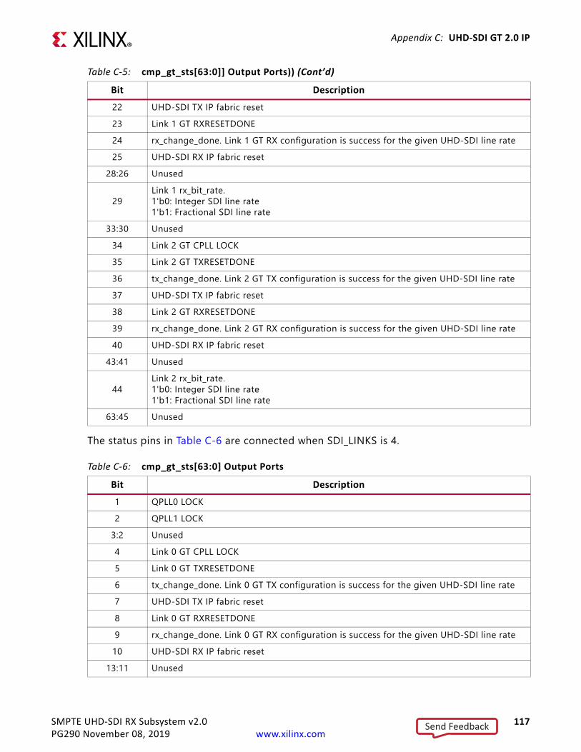
SMPTE UHD-SDI RX Subsystem v2.0 117PG290 November 08, 2019 www.xilinx.com
Appendix C: UHD-SDI GT 2.0 IP
The status pins in Table C-6 are connected when SDI_LINKS is 4.
22 UHD-SDI TX IP fabric reset23 Link 1 GT RXRESETDONE24 rx_change_done. Link 1 GT RX configuration is success for the given UHD-SDI line rate25 UHD-SDI RX IP fabric reset
28:26 Unused
29Link 1 rx_bit_rate.1'b0: Integer SDI line rate1'b1: Fractional SDI line rate
33:30 Unused34 Link 2 GT CPLL LOCK35 Link 2 GT TXRESETDONE36 tx_change_done. Link 2 GT TX configuration is success for the given UHD-SDI line rate37 UHD-SDI TX IP fabric reset38 Link 2 GT RXRESETDONE39 rx_change_done. Link 2 GT RX configuration is success for the given UHD-SDI line rate40 UHD-SDI RX IP fabric reset
43:41 Unused
44Link 2 rx_bit_rate.1'b0: Integer SDI line rate1'b1: Fractional SDI line rate
63:45 Unused
Table C-6: cmp_gt_sts[63:0] Output PortsBit Description1 QPLL0 LOCK2 QPLL1 LOCK
3:2 Unused4 Link 0 GT CPLL LOCK5 Link 0 GT TXRESETDONE6 tx_change_done. Link 0 GT TX configuration is success for the given UHD-SDI line rate7 UHD-SDI TX IP fabric reset8 Link 0 GT RXRESETDONE9 rx_change_done. Link 0 GT RX configuration is success for the given UHD-SDI line rate
10 UHD-SDI RX IP fabric reset13:11 Unused
Table C-5: cmp_gt_sts[63:0]] Output Ports)) (Cont’d)
Bit Description
Send Feedback

SMPTE UHD-SDI RX Subsystem v2.0 118PG290 November 08, 2019 www.xilinx.com
Appendix C: UHD-SDI GT 2.0 IP
14Link 0 rx_bit_rate.1'b0: Integer SDI line rate1'b1: Fractional SDI line rate
15 rx_ce Used only in case of multi link SDI. Receiver clock enable.
18:16
rx_mode[2:0] - Used only in case of multi link SDI. This signal indicates the current SDI mode of the receiver:000 = HD001 = SD010 = 3G100 = 6G101 = 12G 1000/1000110 = 12G 1000/1001When the receiver is not locked and rx_mode_locked output is low, the sdi_mode port changes its values while the receiver searches for the correct SDI mode. When the receiver detects the correct SDI mode, the rx_mode_locked output goes high.
19 Link 1 GT CPLL LOCK20 Link 1 GT TXRESETDONE21 tx_change_done. Link 1 GT TX configuration is success for the given UHD-SDI line rate22 UHD-SDI TX IP fabric reset23 Link 1 GT RXRESETDONE24 rx_change_done. Link 1 GT RX configuration is success for the given UHD-SDI line rate25 UHD-SDI RX IP fabric reset
28:26 Unused
29Link 1 rx_bit_rate.1'b0: Integer SDI line rate1'b1: Fractional SDI line rate
33:30 Unused34 Link 2 GT CPLL LOCK35 Link 2 GT TXRESETDONE36 tx_change_done. Link 2 GT TX configuration is success for the given UHD-SDI line rate37 UHD-SDI TX IP fabric reset38 Link 2 GT RXRESETDONE39 rx_change_done. Link 2 GT RX configuration is success for the given UHD-SDI line rate40 UHD-SDI RX IP fabric reset
43:41 Unused
44Link 2 rx_bit_rate.1'b0: Integer SDI line rate1'b1: Fractional SDI line rate
Table C-6: cmp_gt_sts[63:0] Output Ports (Cont’d)
Bit Description
Send Feedback

SMPTE UHD-SDI RX Subsystem v2.0 119PG290 November 08, 2019 www.xilinx.com
Appendix C: UHD-SDI GT 2.0 IP
48:45 Unused49 Link 3 GT CPLL LOCK50 Link 3 GT TXRESETDONE51 tx_change_done. Link 3 GT TX configuration is success for the given UHD-SDI line rate52 UHD-SDI TX IP fabric reset53 Link 2 GT RXRESETDONE54 rx_change_done. Link 3 GT RX configuration is success for the given UHD-SDI line rate55 UHD-SDI RX IP fabric reset
58:56 Unused
59Link 3 rx_bit_rate. 1'b0: Integer SDI line rate1'b1: Fractional SDI line rate
63:60 Unused
Table C-7: rx_change_fail_code Output Port EncodingCode Description
0 Reserved
1
When a change of the RX SDI mode is requested that requires changing the RXCDR_CFG2 attribute in the GT transceiver, the UHD-SDI control module attempts to do a DRP write cycle to change that attribute. If the UHD-SDI DRP control module detected a mismatch between the written RXCDR_CFG2 value and its actual content after retries, the sequence fails with this failure code
2
When a change of the RX SDI mode is requested that requires changing the RXOUT_DIV attribute in the GT transceiver, the UHD-SDI control module attempts to do a DRP write cycle to change that attribute. If the UHD-SDI DRP control module detected a mismatch between the written RXCDR_CFG2 value and its actual content after retries, the sequence fails with this failure code
3The gtwiz_reset_rx_datapath_in port of the GT Wizard IP is asserted after completing a series for DRP and GT port during a dynamic change to reset the GT RX portion. If the gtwiz_reset_rx_done_out port of GT Wizard IP failed to assert after retries, the sequence fails with this failure code
4
When a change of the RX SDI mode is requested that requires changing the RXDATA_WIDTH attribute in the GT transceiver, the UHD-SDI control module attempts to do a DRP write cycle to change that attribute. If the UHD-SDI DRP control module detected a mismatch between the written RXDATA_WIDTH value and its actual content after retries, the sequence fails with this failure code
5
When a change of the RX SDI mode is requested that requires changing the RXINT_DATAWIDTH attribute in the GT transceiver, the UHD-SDI control module attempts to do a DRP write cycle to change that attribute. If the UHD-SDI DRP control module detected a mismatch between the written RXINT_DATAWIDTH value and its actual content after retries, the sequence fails with this failure code
7-6 Reserved
Table C-6: cmp_gt_sts[63:0] Output Ports (Cont’d)
Bit Description
Send Feedback

SMPTE UHD-SDI RX Subsystem v2.0 120PG290 November 08, 2019 www.xilinx.com
Appendix C: UHD-SDI GT 2.0 IP
Table C-8: tx_change_fail_code Output Port EncodingCode Description
0 Reserved
1
When a change of the TX SDI mode is requested that requires changing the TXDATA_WIDTH attribute in the GT transceiver, the UHD-SDI control module attempts to do a DRP write cycle to change that attribute. If the UHD-SDI DRP control module detected a mismatch between the written TXDATA_WIDTH value and its actual content after retries, the sequence fails with this failure code.
2
When a change of the TX SDI mode is requested that requires changing the TXINTDATA_WIDTH attribute in the GT transceiver, the UHD-SDI control module attempts to do a DRP write cycle to change that attribute. If the UHD-SDI DRP control module detected a mismatch between the written TXINTDATA_WIDTH value and its actual content after retries, the sequence fails with this failure code.
3
When a change of the TX SDI mode is requested that requires changing the TXOUT_DIV attribute in the GT transceiver, the UHD-SDI control module attempts to do a DRP write cycle to change that attribute. If the UHD-SDI DRP control module detected a mismatch between the written TXOUT_DIV value and its actual content after retries, the sequence fails with this failure code.
4The gtwiz_reset_tx_datapath_in port of the GT Wizard IP is asserted after completing a series for DRP and GT port during a dynamic change to reset the GT TX portion. If the gtwiz_reset_tx_done_out port of GT Wizard IP failed to assert after retries, the sequence fails with this failure code.
7-5 Reserved
Table C-9: RX_AXIS4S Interface PortsSignal I/O Description
intf0_rxoutclk O SMPTE SDI RX core clockintf0_rx_axis4s_ch0_tdata O Parallel data received from transceiver.
n varies with SDI standard selection:n=40 for 6G-SDI and 12G-SDIn=20 for 3G-SDI
intf0_rx_axis4s_ch0_tvalid O Data validintf0_rx_axis4s_ch0_tready I SMPTE SDI RX core readyintf0_rx_axis4s_ch0_tlast O Tuser Information. Not used
Send Feedback

SMPTE UHD-SDI RX Subsystem v2.0 121PG290 November 08, 2019 www.xilinx.com
Appendix C: UHD-SDI GT 2.0 IP
ClockingThe UHD-SDI GT core clocking architecture depends on the user selection of QPLL and its associated reference clock. The following table provides details about core clocks.
Table C-10: S_AXIS_STS_SB_RX Interface PortsSignal I/O Description
intf0_ctrl_sb_rx_tdata I Sideband signal information from transceiver block bit 0: rx_change_done—Indicates that SDI line rate is successful bit 2: gtrxresetdone bit 3: rx_m bit 8: rx_fabric_rst—SMPTE UHD-SDI RX IP is reset when this bit set to 1. All other bits are not used
intf0_ctrl_sb_rx_tvalid I Data validintf0_ctrl_sb_rx_tready O Core ready
Table C-11: Core Clock DetailsClock Frequency IP Configuration Notes
drpclk_in 100.0 MHz (Default) All
DRPCLK frequency value valid range is device-dependent. See the respective data sheet for clock range (FGTHDRPCLK for GTH transceiver and FGTYDRPCLK for GTY transceiver)
intf_0_qpll0_refclk_in148.5 MHz for integer SDI line rate or148.35 MHz for fractional SDI line rate
GT COMMON Shared Logic is in core and QPLL0 is selected
This input clock connection depends on PLL reference clock selection
intf_0_qpll1_refclk_in148.5 MHz for integer SDI line rate or148.35 MHz for fractional SDI line rate
GT COMMON Shared Logic is in core and QPLL1 is selected
This input clock connection depends on PLL reference clock selection
intf_0_qpll0out_clk_inFrequency based on GT COMMON configuration and its reference clock frequency
GT COMMON Shared Logic is in example design and QPLL0 is selected
Used to connect to GT CHANNEL primitive
intf_0_qpll0out_refclk_inFrequency based on GT COMMON configuration and its reference clock frequency
GT COMMON Shared Logic is in example design and QPLL0 is selected
Used to connect to GT CHANNEL primitive
Send Feedback

SMPTE UHD-SDI RX Subsystem v2.0 122PG290 November 08, 2019 www.xilinx.com
Appendix C: UHD-SDI GT 2.0 IP
GT COMMON Shared LogicThe UltraScale transceiver architecture has one GT COMMON (GTHE4_COMMON in a GTH-based device or GTYE4_COMMON in a GTY-based device) per quad that can be shared across multiple transceivers. The UHD-SDI transceiver allows the user to generate four SDI links. If the use case is more than four SDI links, clocking from the UHD-SDI GT that has the GT COMMON instantiation can be used for all other SDI links. The UHD-SDI GT (master) has GT COMMON instantiation by selecting Include GT COMMON in the core for the GT COMMON Shared Logic option. Other UHD-SDI GT (slave) cores can share the QPLL clocks outputs from the master UHD-SDI GT core by selecting “Include GT COMMON in example design” for the GT COMMON Shared Logic option.
The following figure shows the sharable resource connections from the UHD-SDI GT core with shared logic included (UHD_SDI_GT_MASTER) to the instance of another UHD-SDI GT core without shared logic (UHD_SDI_GT _SLAVE). QPLL0LOCK and QPLL1LOCK are mapped to cmp_gt_sts[0] and cmp_gt_sts[1] respectively.
intf_0_qpll1out_clk_inFrequency based on GT COMMON configuration and its reference clock frequency
GT COMMON Shared Logic is in example design and QPLL1 is selected
Used to connect to GT CHANNEL primitive
intf_0_qpll1out_refclk_inFrequency based on GT COMMON configuration and its reference clock frequency
GT COMMON Shared Logic is in example design and QPLL1 is selected
Used to connect to GT CHANNEL primitive
Table C-11: Core Clock Details (Cont’d)
Clock Frequency IP Configuration Notes
Send Feedback

SMPTE UHD-SDI RX Subsystem v2.0 123PG290 November 08, 2019 www.xilinx.com
Appendix C: UHD-SDI GT 2.0 IP
Customizing and Generating the CoreThis section includes information about using Xilinx® tools to customize and generate the core in the Vivado Design Suite.
If you are customizing and generating the core in the Vivado IP integrator, see the Vivado Design Suite User Guide: Designing IP Subsystems using IP Integrator (UG994) [Ref 1] for detailed information. IP integrator might auto-compute certain configuration values when validating or generating the design. To check whether the values do change, see the description of the parameter in this chapter. To view the parameter value, run the validate_bd_design command in the Tcl console.
You can customize the IP for use in your design by specifying values for the various parameters associated with the IP core using the following steps:
1. Select the IP from the Vivado IP catalog.2. Double-click the selected IP or select the Customize IP command from the toolbar or
right-click menu.
For details, see the Vivado Design Suite User Guide: Designing with IP (UG896) [Ref 2] and the Vivado Design Suite User Guide: Getting Started (UG910) [Ref 3].
Note: Figures in this chapter are illustrations of the Vivado Integrated Design Environment (IDE). The layout depicted here might vary from the current version.
You can customize the core using the following parameters, or use the defaults.
X-Ref Target - Figure C-3
Figure C-3: Sharable Resource Connections for Shared and Non-Shared Logic
Send Feedback

SMPTE UHD-SDI RX Subsystem v2.0 124PG290 November 08, 2019 www.xilinx.com
Appendix C: UHD-SDI GT 2.0 IP
Core Configuration TabThe following figure shows the Core Configuration tab for customizing the UHD-SDI GT core.
Component Name
The Component Name is the base name of the output files generated for this core.
IMPORTANT: The name must begin with a letter and be composed of the following characters: a to z, A to Z, 0 to 9 and "_."
Core Parameters
• GT Type: Select the GT type. Available options:
° GTHE4 (Default)
° GTYE4• Data Flow: Select the data flow direction
° Duplex (Default)
X-Ref Target - Figure C-4
Figure C-4: UHD-SDI GT IP Configuration
Send Feedback

SMPTE UHD-SDI RX Subsystem v2.0 125PG290 November 08, 2019 www.xilinx.com
Appendix C: UHD-SDI GT 2.0 IP
° RX-Only
Unlike Duplex configuration, the RX-Only selection generates the core without GT TX ports.
• UHD-SDI GT Link(s): Select the number of link(s). Available options:
° 1 (Default)
° 2
° 3
° 4• DRP Clock Freq: Provide the DRP clock frequency in MHz. 100 MHz is the default.• Enable PIXCO Ports: Select this option to use the pixco_fraco IP core in your system.• GT COMMON Shared Logic: Select this option to place GT COMMON within the IP or
outside of the IP. Available options:
° Include GT COMMON in core (Default)
° Include GT COMMON in example design• QPLL0 Ref Clock Selection: Select the reference clock input source. Available options:
° GTREFCLK0 (Default)
° GTREFCLK1
° GTNORTHREFCLK0
° GTNORTHREFCLK1
° GTSOUTHREFCLK0
° GTSOUTHREFCLK1• QPLL1 Ref Clock Selection: Select the reference clock input source. Available options:
° GTREFCLK0
° GTREFCLK1 (Default)
° GTNORTHREFCLK0
° GTNORTHREFCLK1
° GTSOUTHREFCLK0
° GTSOUTHREFCLK1
The following parameters configure clocking for SDI Link 0:
• Link 0 TX Data Width (bits): Select the Link 0 TX data path width used to configure the transceiver TX data path. Select 20 when 3G-SDI is selected in the SMPTE UHD-SDI TX subsystem.
Send Feedback

SMPTE UHD-SDI RX Subsystem v2.0 126PG290 November 08, 2019 www.xilinx.com
Appendix C: UHD-SDI GT 2.0 IP
° 40 (default)
° 20• Link 0 RX Data Width (bits): Select the Link 0 RX data path width used to configure
the transceiver RX data path. Select 20 when 3G-SDI is selected in the SMPTE UHD-SDI RX subsystem.
° 40 (default)
° 20• Link 0 TX PLL1 Type: Select the QPLL for TX UHD-SDI integer line rate data path.
Available options:
° QPLL0
° QPLL1
° CPLL• Link 0 RX PLL1 Type: Select the QPLL for RX UHD-SDI integer line rate data path.
Available options:
° QPLL0
° QPLL1• Link 0 TX PLL2 Type: Select the QPLL for TX UHD-SDI fractional line rate data path.
Available options:
° QPLL0
° QPLL1• Link 0 RX PLL2 Type: Select the QPLL for RX UHD-SDI fractional line rate data path.
Available options:
° QPLL0
° QPLL1
The following parameters configures clocking for SDI Link 1:
• Link 1 TX Data Width (bits): Select the Link 1 TX data path width used to configure the transceiver TX data path. Select 20 when 3G-SDI is selected in the SMPTE UHD-SDI TX subsystem.
° 40 (default)
° 20• Link 1 RX Data Width (bits): Select the Link 1 RX data path width used to configure
the transceiver RX data path. Select 20 when 3G-SDI is selected in the SMPTE UHD-SDI RX subsystem.
° 40 (default)
Send Feedback

SMPTE UHD-SDI RX Subsystem v2.0 127PG290 November 08, 2019 www.xilinx.com
Appendix C: UHD-SDI GT 2.0 IP
° 20• Link 1 TX PLL1 Type: Select the QPLL for TX UHD-SDI integer line rate data path.
Available options:
° QPLL0
° QPLL1• Link 1 RX PLL1 Type: Select the QPLL for RX UHD-SDI integer line rate data path.
Available options:
° QPLL0
° QPLL1• Link 1 TX PLL2 Type: Select the QPLL for TX UHD-SDI fractional line rate data path.
Available options:
° QPLL0
° QPLL1• Link 1 RX PLL2 Type: Select the QPLL for RX UHD-SDI fractional line rate data path.
Available options:
° QPLL0
° QPLL1
The following parameters configure clocking for SDI Link 2:
• Link 2 TX Data Width (bits): Select the Link 2 TX data path width used to configure the transceiver TX data path. Select 20 when 3G-SDI is selected in the SMPTE UHD-SDI TX subsystem.
° 40 (default)
° 20• Link 2 RX Data Width (bits): Select the Link 2 RX data path width used to configure
the transceiver RX data path. Select 20 when 3G-SDI is selected in the SMPTE UHD-SDI RX subsystem.
° 40 (default)
° 20• Link 2 TX PLL1 Type: Select the QPLL for TX UHD-SDI integer line rate data path.
Available options:
° QPLL0
° QPLL1• Link 2 RX PLL1 Type: Select the QPLL for RX UHD-SDI integer line rate data path.
Available options:
Send Feedback

SMPTE UHD-SDI RX Subsystem v2.0 128PG290 November 08, 2019 www.xilinx.com
Appendix C: UHD-SDI GT 2.0 IP
° QPLL0
° QPLL1• Link 2 TX PLL2 Type: Select the QPLL for TX UHD-SDI fractional line rate data path.
Available options:
° QPLL0
° QPLL1• Link 2 RX PLL2 Type: Select the QPLL for RX UHD-SDI fractional line rate data path.
Available options:
° QPLL0
° QPLL1
The following parameters configure clocking for SDI Link 3:
• Link 3 TX Data Width (bits): Select the Link 3 TX data path width used to configure the transceiver TX data path. Select 20 when 3G-SDI is selected in the SMPTE UHD-SDI TX subsystem.
° 40 (default)
° 20• Link 3 RX Data Width (bits): Select the Link 3 RX data path width used to configure
the transceiver RX data path. Select 20 when 3G-SDI is selected in the SMPTE UHD-SDI RX subsystem.
° 40 (default)
° 20• Link 3 TX PLL1 Type: Select the QPLL for TX UHD-SDI integer line rate data path.
Available options:
° QPLL0
° QPLL1• Link 3 RX PLL1 Type: Select the QPLL for RX UHD-SDI integer line rate data path.
Available options:
° QPLL0
° QPLL1• Link 3 TX PLL2 Type: Select the QPLL for TX UHD-SDI fractional line rate data path.
Available options:
° QPLL0
° QPLL1
Send Feedback

SMPTE UHD-SDI RX Subsystem v2.0 129PG290 November 08, 2019 www.xilinx.com
Appendix C: UHD-SDI GT 2.0 IP
• Link 3 RX PLL2 Type: Select the QPLL for RX UHD-SDI fractional line rate data path. Available options:
° QPLL0
° QPLL1
User ParametersThe following table shows the relationship between the parameters in the Vivado IDE and the user parameters (which can be viewed in the Tcl Console).
Table C-12: Vivado IDE Parameter to User Parameter RelationshipVivado IDE Parameter User Parameter Default Value
Core ParametersGT Type C_GT_TYPE GTHE4Data Flow C_DATA_FLOW DuplexSDI link(s) C_SDI_LINKS 1GT COMMON Shared Logic SupportLevel 1 (include GT COMMON in the core)GT QPLL0 Ref Clock Selection C_QPLL0_Refclk_Sel GTREFCLK0
GT QPLL1 Ref Clock Selection C_QPLL1_Refclk_Sel GTREFCLK1
GT CPLL Ref Clock Selection C_CPLL_Refclk_Sel GTREFCLK0DRP Clock Frequency C_DRP_CLK_FREQ 100.0
SDI Link 0Link 0 TX PLL1 Type C_Tx_PLL_Selection_INTF_0
No default value is assigned. User selection is mandatory.
Link 0 RX PLL1 Type C_Rx_PLL_Selection_INTF_0Link 0 TX PLL2 Type C_Tx_PLL2_Selection_INTF_0Link 0 RX PLL2 Type C_Rx_PLL2_Selection_INTF_0
SDI Link 1Link 1 TX PLL1 Type C_Tx_PLL_Selection_INTF_1
No default value is assigned. User selection is mandatoryLink 1 RX PLL1 Type C_Rx_PLL_Selection_INTF_1
Link 1 TX PLL2 Type C_Tx_PLL2_Selection_INTF_1
Link 1 RX PLL2 Type C_Rx_PLL2_Selection_INTF_1 No default value is assigned. User selection is mandatory
Send Feedback

SMPTE UHD-SDI RX Subsystem v2.0 130PG290 November 08, 2019 www.xilinx.com
Appendix C: UHD-SDI GT 2.0 IP
Output GenerationFor details, see the Vivado Design Suite User Guide: Designing with IP (UG896) [Ref 2].
Constraining the CoreThis section contains information about constraining the core in the Vivado Design Suite.
Required ConstraintsThis section defines the additional constraint requirements for the core. Constraints are provided with a Xilinx Design Constraints (XDC) file. An XDC is provided with the HDL example design to give a starting point for constraints for your design.
Device, Package, and Speed Grade SelectionsThis section is not applicable for this IP core.
Clock Frequenciesdrpclk_in should be specified using the following command:
create_clock -name drp_clk -period 10.000 [get_ports drpclk_in]
This constraint defines the frequency of drpclk_in that is supplied to DRP control logic and connected to DRPCLK of GT CHANNEL primitive.
SDI Link 2Link 2 TX PLL1 Type C_Tx_PLL_Selection_INTF_2
No default value is assigned. User selection is mandatory
Link 2 RX PLL1 Type C_Rx_PLL_Selection_INTF_2Link 2 TX PLL2 Type C_Tx_PLL2_Selection_INTF_2Link 2 RX PLL2 Type C_Rx_PLL2_Selection_INTF_2
SDI Link 3Link 3 TX PLL1 Type C_Tx_PLL_Selection_INTF_3
No default value is assigned. User selection is mandatory
Link 3 RX PLL1 Type C_Rx_PLL_Selection_INTF_3Link 3 TX PLL2 Type C_Tx_PLL2_Selection_INTF_3Link 3 RX PLL2 Type C_Rx_PLL2_Selection_INTF_3
Table C-12: (Cont’d)Vivado IDE Parameter to User Parameter RelationshipVivado IDE Parameter User Parameter Default Value
Send Feedback

SMPTE UHD-SDI RX Subsystem v2.0 131PG290 November 08, 2019 www.xilinx.com
Appendix C: UHD-SDI GT 2.0 IP
Clock ManagementThis section is not applicable for this IP core.
Clock PlacementThis section is not applicable for this IP core.
BankingThis section is not applicable for this IP core.
Transceiver PlacementThe UHD-SDI GT core does not have the ability to constrain the transceiver. Constraining the txp, txn, rxp, and rxn ports of GTHE4_CHANNEL/GTYE4_CHANNEL is sufficient for transceiver placement.
I/O Standard and PlacementThis section is not applicable for this IP core.
I/O PlanningThe UHD-SDI GT core generates clock constraints and necessary false path constraints. But it does not constrain GT locations and reference clock locations. See the respective board user guide or board schematic for LOC and add the constraints to the top level xdc file.
Send Feedback

SMPTE UHD-SDI RX Subsystem v2.0 132PG290 November 08, 2019 www.xilinx.com
Appendix D
Audio Test Pattern Generator IPThis appendix provides information on Audio Test Pattern Generator IP core (audio_tpg_v1_0) that is used in UHD-SDI Subsystems example designs and provides details on register programming. This IP core is hidden in catalogue and can be generated only in IP integrator canvas using the create_bd_cell Tcl command.
Feature Summary• AXI4S compliant • 16/24 bit data support • Support for 2,4,6,8...32 channels• 1K, 2K sine tones and incremental pattern generation• Checker block for validating incoming incremental pattern• Generate and consume mode• Audio sampling can be changed at runtime
Unsupported Features, Limitations • No 20 bit data support• Checker supports only incremental pattern• Same data on is sent over all left channels and all right channels for sine tone outputs.• Supports only 32K, 44.1K and 48K audio sampling• 1K and 2K sine tone outputs
Send Feedback

SMPTE UHD-SDI RX Subsystem v2.0 133PG290 November 08, 2019 www.xilinx.com
Appendix D: Audio Test Pattern Generator IP
Port Descriptions
Register SpaceThe Audio Pattern Generator (PatGen) IP register space is shown in Table D-2.
Table D-1: Port DescriptionsSignal Name Interface Type Description
s_axi_aclk Clock Input Input clock for AXI4Lite Interface
s_axi_aresetn reset Input Active-Low reset for AXI4Lite Interface
s_axi_* s_axi_ctrl AXI-Lite Interface
aud_mclk Clock Input Input audio clock. Typically a multiple of Fs
m_axis_aud_aclk Clock Input AXIS Audio streaming clockm_axis_aud_resetn Reset Input Active-Low AXIS audio resetm_axis_aud_* Audio AXIS Interface Master Master AXIS audio interfaces_axis_aud_* Audio AXIS Interface Slave Slave AXIS audio interface
m_aud_pulse Signal Output Pulse on aud_clk with sample frequency
Table D-2: Audio Pattern Generator Register SpaceReg Offset Name Reg Description
0x00 Control Register Control register0x04 Fs Multiplier Register to specify Fs multiplier
0x08 Patgen Configuration PatGen configuration such as channels, pattern, sampling and data width
0x0C Silence time register Specify any silence time to create a beep pattern0x10-0x24 Channel Status Bits Specify the 192 bits channel status0x28-0x3C User Status bits Specify the 192 bits user bits
0x40 Validity register Set the validity bit for samples0x44 Checker Status To check the checker result0x48 Valid sample counter Counts the number valid samples that were checked
0x4C Number of samplesmissed counter Counts number data mismatches that occurred
0x50 Data received Incoming data sample register0x54 Previous data Previous sampled data register
Send Feedback

SMPTE UHD-SDI RX Subsystem v2.0 134PG290 November 08, 2019 www.xilinx.com
Appendix D: Audio Test Pattern Generator IP
Note: The AXI4-Lite write access register is updated by the 32-bit AXI Write Data (*_wdata) signal, and is not impacted by the AXI Write Data Strobe (*_wstrb) signal. For a Write, both the AXI Write Address Valid (*_awvalid) and AXI Write Data Valid (*_wvalid) signals should be asserted together.
Core Control Register (0x00)This register is used to control the APG and change its behavior to either generate audio traffic or put it in by-pass mode. The APG, by default, is in bypass mode. When APG is to be started, by-pass should be disabled.
Note: All of the following registers, except 0x40, can be written only when the ‘Enable APG’ bit of Core Control Register is 0. All of the following registers have to be programmed first before starting the APG.
Fs Multiplier Register (0x04)Program this register to specify the multiplier value of the aud_clk.
Table D-3: Core Control Register
Name DefaultValue Access Description
Bypass enable 0x1 RW
[31]This bit is used to enable the bypass mode. In this mode the APG is bypassed and whatever that comes on input AXIS is forwarded to output AXIS interface. This bit has a higher priority than bit [0].
Reserved [30:2]
Start Checker 0x0 RW[1]This bit enables the checker. Checker keeps checking the AXIS data received from the S_AXIS ports.
Enable APG 0x0 RW[0]Set this bit to start the APG or put in generate mode. This should be enabled after all other config registers have been written.
Table D-4: Fs Multiplier Register
Name DefaultValue Access Description
RSVD [31:16]
Multi Value 0x180 RW
[15:0]Specify the multiplier value of the aud_clk. For example, for Fs = 48Khz, the supplied aud_clk is 18.432Mhz, then this register should be programmed with a value of 384. i.e. 48Khz * 384 = 18.432Mhz
Send Feedback

SMPTE UHD-SDI RX Subsystem v2.0 135PG290 November 08, 2019 www.xilinx.com
Appendix D: Audio Test Pattern Generator IP
APG Config Register (0x08)This registers provides capability to enable/disable the core.
APG Silence Register (0x0C)This register is used to insert a silence time. This can be programmed to create a beep pattern of either 1Kh or 2Khz sine wave.
Table D-5: APG Config Register
Name DefaultValue Access Description
Channel count 0x2 RW [31:24] Set number of audio channels. Valid values are 2, 4, 6 and 8.
Data width 0x4 RW
[23:16]Specify the width of audio data samples. Valid values are:001 – 16 bit audio samples010 – 20 bit audio samples100 – 24 bit audio samples
Sampling Frequency 0x2 RW
[15:8]Specify the sampling rate of the audio samples. Valid values are:000 – 32Khz001 – 44.1Khz010 – 48Khz
Pattern 0x0 R/W
[7:0]Select from internal patterns. Valid values are:000 – 1Khz sine wave001 – 2Khz sine wave010 – 1Khz sine wave on left, 2Khz sine wave on right channel111 – Incremental pattern
Table D-6: APG Silence Register
Name DefaultValue Access Description
Reserved 0 [31:16]
Silence interval 0 RW
[15:0]Specify a value to insert periodic silence. The silence time is twice the value that is programmed here. Silence time = 2*value*aud_clk PeriodA value of 0 means no silence.
Send Feedback

SMPTE UHD-SDI RX Subsystem v2.0 136PG290 November 08, 2019 www.xilinx.com
Appendix D: Audio Test Pattern Generator IP
Channel Status Register (0x10-0x24)Specify the 192bits of Channels Status information using these 6 registers. Each register is to be programmed with 32 bits of data in order of LSB to MSB.
User Info Register (0x28-0x3C)Specify the 192bits of User information using these 6 registers. Each register is to be programmed with 32 bits of data in order of LSB to MSB.
Validity Control (0x40)This bit allows the user to set the validity bit in the Audio sample.
Table D-7: Channel Status Register
Name DefaultValue Access Description
Channel Status 0 RW [31:0] Specify the 32 bit information.
Table D-8: User Info Register
Name DefaultValue Access Description
User info 0 RW [31:0] Specify the 32 bit information.
Table D-9: Validity Control
Name DefaultValue Access Description
Reserved 0 [31:1]
Validity 0x0 R/W
[0]This bit can be used to set the validity bit inside the audio sample frame. Receivers typically ignore the samples, which have the validity bit set to ‘1’.
Send Feedback
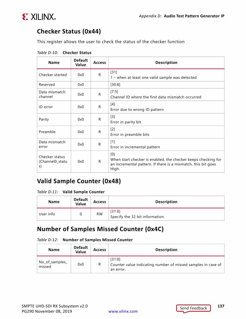
SMPTE UHD-SDI RX Subsystem v2.0 137PG290 November 08, 2019 www.xilinx.com
Appendix D: Audio Test Pattern Generator IP
Checker Status (0x44)This register allows the user to check the status of the checker function
Valid Sample Counter (0x48)
Number of Samples Missed Counter (0x4C)
Table D-10: Checker Status
Name DefaultValue Access Description
Checker started 0x0 R [31]1 – when at least one valid sample was detected
Reserved 0x0 [30:8]Data mismatch channel 0x0 R [7:5]
Channel ID where the first data mismatch occurred
ID error 0x0 R [4]Error due to wrong ID pattern
Parity 0x0 R [3]Error in parity bit
Preamble 0x0 R [2]Error in preamble bits
Data mismatch error 0x0 R [1]
Error in incremental pattern
Checker status (Channel0_status)
0x0 R[0]When start checker is enabled, the checker keeps checking for an incremental pattern. If there is a mismatch, this bit goes High.
Table D-11: Valid Sample Counter
Name DefaultValue Access Description
User info 0 RW [31:0] Specify the 32 bit information.
Table D-12: Number of Samples Missed Counter
Name DefaultValue Access Description
No_of_samples_missed 0x0 R
[31:0] Counter value indicating number of missed samples in case of an error.
Send Feedback

SMPTE UHD-SDI RX Subsystem v2.0 138PG290 November 08, 2019 www.xilinx.com
Appendix D: Audio Test Pattern Generator IP
Data Received (0x50)This register gives the information of the incoming data sample when the first data mismatch error occurred.
Previous Data (0x54)This register stores the previous sampled data available when the data mismatch error occurred.
A data mismatch error occurs when incoming data is not equal to the previously sampled data + 1.
ClockingThere are three possible clock inputs available:
• s_axi_aclk: AXI4-Lite control interface clock• aud_aclk: Reference audio MCLK. This is typically a multiple of Fs (for example, Fs*384).• m_axis_aud_aclk: AXIS streaming interface clock
ResetsThe s_axi_aresetn resets the register interface and all puts all the registers in their default state.
Table D-13: Data Received
Name DefaultValue Access Description
Reserved [31:24]
Incoming data 0x0 R [23:0]Data received on s_aud_tdata when the error occurred.
Table D-14: Previous Data
Name DefaultValue Access Description
Reserved [31:24]
Sampled data 0x0 R[23:0]Previous sampled data when error occurred.Current data should be sampled data + 1
Send Feedback

SMPTE UHD-SDI RX Subsystem v2.0 139PG290 November 08, 2019 www.xilinx.com
Appendix D: Audio Test Pattern Generator IP
Programming SequenceThe APG can be put in generate-consume mode using the following programming sequence:
1. Setup the APG configuration registers for no of channels, data width, sampling, and pattern.Note: These values cannot be updated after the APG is started.
2. Program the Multiplier value. Program the channel status and user bits.Note: The multiplier value should match with the aud_clk frequency
3. Program the Control registers to put the APG in generate mode. Note: In this mode, the APG outputs the audio samples and at the same time consumes the audio on AXIS slave interface by asserting ready.
To change the APG to bypass mode, simply program the Control register bit [31] to ‘1’. All other registers are ignored when APG is set in the bypass mode. Irrespective of the APG mode (generate or bypass), the checker can be enabled by programming the Control Register bit [1] to 1.
Note: In bypass mode, the APG connects the Master and Slave AXIS interfaces. In generate-consume mode, the APG continuously generates the samples at a programmed rate. A small buffer is available which can overflow if the samples are not consumed.
Send Feedback

SMPTE UHD-SDI RX Subsystem v2.0 140PG290 November 08, 2019 www.xilinx.com
Appendix E
Additional Resources and Legal Notices
Xilinx ResourcesFor support resources such as Answers, Documentation, Downloads, and Forums, see Xilinx Support.
Documentation Navigator and Design HubsXilinx Documentation Navigator provides access to Xilinx documents, videos, and support resources, which you can filter and search to find information. To open the Xilinx Documentation Navigator (DocNav):
• From the Vivado IDE, select Help > Documentation and Tutorials.• On Windows, select Start > All Programs > Xilinx Design Tools > DocNav.• At the Linux command prompt, enter docnav.
Xilinx Design Hubs provide links to documentation organized by design tasks and other topics, which you can use to learn key concepts and address frequently asked questions. To access the Design Hubs:
• In the Xilinx Documentation Navigator, click the Design Hubs View tab.• On the Xilinx website, see the Design Hubs page.Note: For more information on Documentation Navigator, see the Documentation Navigator page on the Xilinx website.
Send Feedback

SMPTE UHD-SDI RX Subsystem v2.0 141PG290 November 08, 2019 www.xilinx.com
Appendix E: Additional Resources and Legal Notices
ReferencesThese documents provide supplemental material useful with this product guide:
1. Vivado® Design Suite User Guide: Designing IP Subsystems using IP Integrator (UG994)2. Vivado Design Suite User Guide: Designing with IP (UG896)3. Vivado Design Suite User Guide: Getting Started (UG910)4. Vivado Design Suite User Guide: Logic Simulation (UG900)5. ISE® to Vivado Design Suite Migration Guide (UG911)6. Vivado Design Suite User Guide: Programming and Debugging (UG908)7. Vivado Design Suite User Guide - Implementation (UG904)8. LogiCORE IP AXI4-Stream to Video Out Product Guide (PG044)9. SMPTE UHD-SDI Product Guide (PG205)10. Video In to AXI4-Stream LogiCORE IP Product Guide (PG043)11. AXI4-Stream Video IP and System Design Guide (UG934)12. UltraScale Architecture GTH Transceivers User Guide (UG576)13. Ultrascale Architecture GTY Transceivers User Guide (UG578)14. UltraScale FPGAs Transceivers Wizard (PG182) 15. Kintex UltraScale+ FPGAs Data Sheet: DC and AC Switching Characteristics (DS922)16. SMPTE UHD-SDI TX Subsystem Product Guide (PG289)17. Vivado Design Suite: AXI Reference Guide (UG1037)18. UHD-SDI Audio Core IP Product Guide (PG309)
Send Feedback

SMPTE UHD-SDI RX Subsystem v2.0 142PG290 November 08, 2019 www.xilinx.com
Appendix E: Additional Resources and Legal Notices
Revision HistoryThe following table shows the revision history for this document.
Please Read: Important Legal NoticesThe information disclosed to you hereunder (the “Materials”) is provided solely for the selection and use of Xilinx products. To the maximum extent permitted by applicable law: (1) Materials are made available “AS IS” and with all faults, Xilinx hereby DISCLAIMS ALL WARRANTIES AND CONDITIONS, EXPRESS, IMPLIED, OR STATUTORY, INCLUDING BUT NOT LIMITED TO WARRANTIES OF MERCHANTABILITY, NON-INFRINGEMENT, OR FITNESS FOR ANY PARTICULAR PURPOSE; and (2) Xilinx shall not be liable (whether in contract or tort, including negligence, or under any other theory of liability) for any loss or damage of any kind or nature related to, arising under, or in connection with, the Materials (including your use of the Materials), including for any direct, indirect, special, incidental, or consequential loss or damage (including loss of data, profits, goodwill, or any type of loss or damage suffered as a result of any action brought by a third party) even if such damage or loss was reasonably foreseeable or Xilinx had been advised of the possibility of the same. Xilinx assumes no obligation to correct any errors contained in the Materials or to notify you of updates to the Materials or to product specifications. You may not reproduce, modify, distribute, or publicly display the Materials without prior written consent. Certain products are subject to the terms and conditions of Xilinx's limited warranty, please refer to Xilinx's Terms of Sale which can be viewed at https://www.xilinx.com/legal.htm#tos; IP cores may be subject to warranty and support terms contained in a license issued to you by Xilinx. Xilinx products are not designed or intended to be fail-safe or for use in any application requiring fail-safe performance; you assume sole risk and liability for use of Xilinx products in such critical applications, please refer to Xilinx's Terms of Sale which can be viewed at https://www.xilinx.com/legal.htm#tos.AUTOMOTIVE APPLICATIONS DISCLAIMER
Date Version Revision11/08/2019 2.0 • Added Table A-1, Table A-5, Table C-9, and Table C-10.
• Updated Table 2-8, Table 2-12, Table 5-1, Table C-4, Table C-5, Table C-6, and Table C-12.
• Updated Features.• Updated Unsupported Features.• Updated Requirements.• Updated SDK instances to Vitis software platform.• Updated Vivado menu commands.
07/30/2019 2.0 • Updated Figure C-2 and Figure C-4.• Updated Component Name.• Updated Table 2-8, Table C-2, Table C-3, and Table C-12.• Added Figure 5-21.
12/05/2018 2.0 • Updated UHD-SDI Audio Extract Use Case• Updated ZCU106 SMPTE UHD-SDI Audio-Video Pass-Through Example
Design• Updated Table 5-2 and HD-SDI TXOUTCLK frequencies• Added UHD-SDI GT Ports• Added RX_ST352_DATA_DS<n> registers for C stream
04/04/2018 2.0 • Added ZCU106 UHD-SDI Audio-Video Pass-Through Example Design• Added KCU116 UHD-SDI Audio-Video Loopback Example Design• Added Appendix C for UHD-SDI IP• Added Appendix D for Audio Test Pattern Generator IP
10/04/2017 1.0 Initial Xilinx release.
Send Feedback

SMPTE UHD-SDI RX Subsystem v2.0 143PG290 November 08, 2019 www.xilinx.com
Appendix E: Additional Resources and Legal Notices
AUTOMOTIVE PRODUCTS (IDENTIFIED AS “XA” IN THE PART NUMBER) ARE NOT WARRANTED FOR USE IN THE DEPLOYMENT OF AIRBAGS OR FOR USE IN APPLICATIONS THAT AFFECT CONTROL OF A VEHICLE (“SAFETY APPLICATION”) UNLESS THERE IS A SAFETY CONCEPT OR REDUNDANCY FEATURE CONSISTENT WITH THE ISO 26262 AUTOMOTIVE SAFETY STANDARD (“SAFETY DESIGN”). CUSTOMER SHALL, PRIOR TO USING OR DISTRIBUTING ANY SYSTEMS THAT INCORPORATE PRODUCTS, THOROUGHLY TEST SUCH SYSTEMS FOR SAFETY PURPOSES. USE OF PRODUCTS IN A SAFETY APPLICATION WITHOUT A SAFETY DESIGN IS FULLY AT THE RISK OF CUSTOMER, SUBJECT ONLY TO APPLICABLE LAWS AND REGULATIONS GOVERNING LIMITATIONS ON PRODUCT LIABILITY.© Copyright 2017–2019 Xilinx, Inc. Xilinx, the Xilinx logo, Alveo, Artix, Kintex, Spartan, Versal, Virtex, Vivado, Zynq, and other designated brands included herein are trademarks of Xilinx in the United States and other countries. AMBA, AMBA Designer, Arm, ARM1176JZ-S, CoreSight, Cortex, PrimeCell, Mali, and MPCore are trademarks of Arm Limited in the EU and other countries. All other trademarks are the property of their respective owners.
Send Feedback