slus601–may 2005 midrange input synchronous buck
TRANSCRIPT

www.ti.com
FEATURES APPLICATIONS
DESCRIPTION
TYPICAL APPLICATION
TPS40100
1
3
18
16
2
4
17
15
5
6
14
13
24 2223 21 20 19
7 98 10 11 12
COMP
FB
TRKOUT
TRKIN
UVLO
ILIM
MG
U
MG
D
SY
NC
PG
VO
ISN
S
RT
BIA
S
GN
D
SS
GM
PG
ND
VDD
SW
HDRV
BST
5VBP
LDRV
UDG−04137
VIN VTRKIN
VIN
TPS40100
SLUS601–MAY 2005
MIDRANGE INPUT SYNCHRONOUS BUCK CONTROLLERWITH ADVANCED SEQUENCING AND OUTPUT MARGINING
• Servers• Operation over 4.5 V to 18 V Input Range• Networking Equipment• Adjustable Frequency (Between 100 kHz and• Cable Modems and Routers600 kHz) Current Feedback Control• XDSL Modems and Routers• Output Voltage Range From 0.7 V to 5.5 V• Set-Top Boxes• Simultaneous, Ratiometric and Sequential• Telecommunications EquipmentStartup Sequencing• Power Supply Modules• Adaptive Gate Drive
• Remote Sensing (Via Separate GND/PGND)• Internal Gate Drivers for N-channel MOSFETs
The TPS40100 is a mid voltage, wide-input (between• Internal 5-V Regulator4.5 V and 18 V), synchronous, step-down controller.
• 24-Pin QFN Package The TPS40100 offers programmable closed loopsoft-start, programmable UVLO (with programmable• Thermal Shutdownhysteresis), programmable inductor sensed current• Programmable Overcurrent Protectionlimit and can be synchronized to other timebases.
• Power Good Indicator The TPS40100 incorporates MOSFET gate drivers• 1%, 690-mV Reference for external N-channel high-side and synchronous
rectifier (SR) MOSFET. Gate drive logic incorporates• Output Margining, 3% and 5%adaptive anti-cross conduction circuitry for improved
• Programmable UVLO (with Programmable efficiency, reducing both cross conduction and diodeHysteresis) conduction in the rectifier MOSFET. The externally
• Frequency Synchronization programmable current limit provides a hiccupovercurrent recovery characteristic.
Please be aware that an important notice concerning availability, standard warranty, and use in critical applications of TexasInstruments semiconductor products and disclaimers thereto appears at the end of this data sheet.
PRODUCTION DATA information is current as of publication date. Copyright © 2005, Texas Instruments IncorporatedProducts conform to specifications per the terms of the TexasInstruments standard warranty. Production processing does notnecessarily include testing of all parameters.
www.ti.com
ABSOLUTE MAXIMUM RATINGS
TPS40100
SLUS601–MAY 2005
ORDERING INFORMATION
TA PACKAGE PART NUMBER(1)
TPS40100RGER-40°C to 85°C QFN
TPS40100RGET
(1) The QFN package (RGE) is available taped and reeled only. Uselarge reel device type R (TPS40100RGER) to order quantities of3,000 per reel. Use small reel device type T (TPS40100RGET) toorder quantities of 250 per reel.
over operating free-air temperature range unless otherwise noted(1)
TPS40100 UNIT
VDD -0.3 to 20
5VBP, BIAS, FB, ILIM, ISNS, LDRV, MGU, MGD, PG, SS, -0.3 to 6SYNC, UVLO, VO
BST to SW, HDRV to SW(2) -0.3 to 6.0
SW -1.5 to VVINVIN Input voltage range VSW (transient) < 100 ns -6 to 30
TRKIN -0.3 to 20
GND to PGND -0.3 to 0.3
TRKOUT -0.3 to 8.0
HDRV, LDRV (RMS) 0.5A
HDRV, LDRV (peak) 2.0
FB, COMP, TRKOUT 10 to -10 mA
SS 20 to -20
IIN Input current range PG 20
GM 1 mA
RT 10
V5BP 50(3)
RT source 100 µA
TJ Operating junction temperature range –40 to 125°C
Tstg Storage temperature –55 to 150
(1) Stresses beyond those listed under "absolute maximum ratings" may cause permanent damage to the device. These are stress ratingsonly, and functional operation of the device at these or any other conditions beyond those indicated under "recommended operatingconditions" is not implied. Exposure to absolute-maximum-rated conditions for extended periods may affect device reliability.
(2) BST to SW and HDRV to SW are relative measurements. BST and HDRV can be this amount of voltage above or below the voltage atSW.
(3) V5BP current includes gate drive current requirements. Observe maximum TJ rating for the device.
2

www.ti.com
ELECTRICAL CHARACTERISTICS
TPS40100
SLUS601–MAY 2005
-40°C ≤ TA = TJ≤ 85°C, VVDD = 12 V, RRT = 182 kΩ, RGM = 232 kΩ, RILIM = 121 kΩ (unless otherwise noted)
PARAMETER TEST CONDITIONS MIN TYP MAX UNIT
INPUT VOLTAGE
VVDD Operating range 4.5 18.0 V
OPERATING CURRENT
IDD Quiescent current VFB > 0.8 V, 0% duty cycle 1.3 1.8 2.5 mA
ISD Shutdown current VUVLO < 1 V 500 µA
5VPB
7 V ≤ VVDD≤ 18 V, 0 mA ≤ ILOAD≤ 30 mA 4.7 5.0 5.3Internal regulator V
4.5 V ≤ VVDD < 7 V, 0 mA ≤ ILOAD≤ 30 mA 4.3 5.0 5.3
OSCILLATOR/RAMP GENERATOR
fSW Programmable oscillator frequency 100 600kHz4.5 V ≤ VVDD < 18 V,Oscillator frequency accuracy 250 275 300-40°C ≤ TA = TJ≤ 125°C
VRAMP Ramp amplitude(1) 0.5 VP-PtOFF Fixed off-time 100 150 ns
DMIN Minimum duty cycle 0%
tMIN Minimum controllable pulse width(1) CLOAD = 4.7 nF, -40°C ≤ TA = TJ≤ 125°C 175 ns
VVLY Valley voltage(1) 1.0 1.6 2.0 V
FREQUENCY SYNCHRONIZATION
VIH High-level input voltage 2V
VIL Low-level input voltage 0.8
ISYNC Input current, SYNC VSYNC = 2.5 V 4.0 5.5 10.0 µA
tSYNC Mimimum pulse width, SYNC 50ns
tSYNC_SH Minimum set-up/hold time, SYNC(2) 100
SOFT-START AND FAULT IDLE
ISS Soft-start source (charge) current 13 20 25µA
ISS_SINK Soft-start sink (discharge) current 3.4 5.0 6.6
VSSC Soft-start completed voltage 3.25 3.40 3.75V
VSSD Soft-start discharged voltage 0.15 0.20 0.25
Retry interval time to SS time ratio(1) 16
VSSOS Offset from SS to error amplifier 300 500 800 mV
ERROR AMPLIFIER
GBWP Gain bandwidth product(1) 3.5 5.0 MHz
AVOL Open loop 60 80 dB
IBIAS Input bias current, FB 50 200 nA
IOH High-level output current 2 3mA
IOL Low-level output current 2 3
Slew rate(1) 2.1 V/µs
FEEDBACK REFERENCE
TA =25°C 686 690 694VFB Feedback voltage reference mV
-40°C < TA = TJ≤ 125°C 683 697
(1) Ensured by design. Not production tested.(2) To meet set up time requirements for the synchronization circuit, a negative logic pulse must be greater than 100 ns wide.
3
www.ti.com
TPS40100
SLUS601–MAY 2005
ELECTRICAL CHARACTERISTICS (continued)
-40°C ≤ TA = TJ≤ 85°C, VVDD = 12 V, RRT = 182 kΩ, RGM = 232 kΩ, RILIM = 121 kΩ (unless otherwise noted)
PARAMETER TEST CONDITIONS MIN TYP MAX UNIT
VOLTAGE MARGINING
Feedback voltage margin 5% up VMGU ≤ 500 mV 715 725 735VFBMGU mV
Feedback voltage margin 3% up 2 V ≤ VMGU ≤ 3 V 700 711 720
IMGUP Margin-up bias current 60 80 100 µA
Feedback voltage margin 5% down VMGD ≤ 500 mV 645 655 665VFBMGD mA
Feedback voltage margin 3% down 2 V ≤ VMGD ≤ 3 V 660 669 680
IMGDN Margin-down bias current 60 80 100 µA
tMGDLY Margining delay time(3) 12 30ms
tMGTRAN Margining transition time 1.5 7.0
CURRENT SENSE AMPLIFIER
gmCSA Current sense amplifier gain TJ =25°C 300 333 365 µS
TCGM Amplifier gain temperature coefficient -2000 ppm/°C
VGMLIN Gm linear range voltage TJ =25°C -50 50 mV
IISNS Bias current at ISNS pin VVO = VISNS = 3.3 V 250 nA
0 6VGMCM Input voltage common mode V
4.5 V ≤ VIN ≤ 5.5 V 0 3.6
CURRENT LIMIT
VILIM ILIM pin voltage to trip overcurrent 1.44 1.48 1.52 V
tILIMDLY Current limit comparator propagation delay HDRV transition from on to off 70 140 ns
DRIVER SPECIFICATIONS
tRHDRV HIgh-side driver rise time(4) CLOAD = 4.7 nF 57ns
tFHDRV HIgh-side driver fall time(4) CLOAD = 4.7 nF 47
IHDRVSRPKS HIgh-side driver peak source current(4) 800mA
IHDRVSRMIL HIgh-side driver source current at 2.5 V(4) VHDRV - VSW = 2.5 V 700
IHSDVSNPK HIgh-side driver peak sink current(4) 1.3A
IHDRVSNMIL High-side driver sink current at 2.5 V(4) VHDRV - VSW = 2.5 V 1.2
RHDRVUP HIgh-side driver pullup resistance IHDRV = 300 mA 2.4 4.0Ω
RHDRVDN HIgh-side driver pulldown resistance IHDRV = 300 mA 1.0 1.8
tRLDRV Low-side driver rise time(4) CLOAD = 4.7 nF 57ns
tFLDRV Low-side driver fall time(4) CLOAD = 4.7 nF 47
ILDRVSRPK Low-side driver peak source current(4) 800mA
ILDRVSNMIL Low-side driver source current at 2.5 V(4) VLDRV = 2.5 V 700
ILSDVSNPK Low-side driver peak sink current(4) 1.3A
Low-side driver sink current at 2.5 V(4) VLDRV = 2.5 V 1.2
RLDRVUP Low-side driver pullup resistance ILDRV = 300 mA 2.0 4.0Ω
RLDRVDN Low-side driver pulldown resistance ILDRV = 300 mA 0.8 1.5
ISWLEAK Leakage current from SW pin -1 1 µA
POWERGOOD
VLPGD Powergood low voltage IPGD= 2 mA 30 100 mV
tPGD Powergood delay time 15 25 35 µs
VVDD = OPEN, 10-kΩ pullup to externalVLPGDNP Powergood low voltage , no device power 1.00 1.25 V5-V supply
VOV Power good overvoltage threshold, VFB 765mV
VUV Power good undervoltage threshold, VFB 615
(3) Margining delay time is the time delay from an assertion of a margining command until the output voltage begins to transition to themargined voltage.
(4) Ensured by design. Not production tested.
4

www.ti.com
DEVICE INFORMATION
RT
BIAS
GND
SS
GM
PGND
7
8
9
10
11
12
RGE PACKAGE(BOTTOM VIEW)
24
23
22
21
20
19
MGU
MGD
SYNC
PG
VO
ISNS
1 2 3 4 5 6
18 17 16 15 14 13
COMP
FB
TRKOUT
TRKIN
UVLO
ILIM
VDD
SW
HDRV
BST
5VBP
LDRV
TPS40100
SLUS601–MAY 2005
ELECTRICAL CHARACTERISTICS (continued)
-40°C ≤ TA = TJ≤ 85°C, VVDD = 12 V, RRT = 182 kΩ, RGM = 232 kΩ, RILIM = 121 kΩ (unless otherwise noted)
PARAMETER TEST CONDITIONS MIN TYP MAX UNIT
TRACKING AMPLIFIER
VTRKOS = VTRKIN - VO ; VVO≤ 2 V 7 25 40VTRKOS Tracking amplifier input offset voltage mV
VTRKOS = VTRKIN - VO ; 2 V < VVO≤ 6 V -5 25 40
VTRKCM Input common mode, active range 0 6
4.5 V ≤ VVDD ≤ 5.5 V 0 3.6VTRK Tracking amplifier voltage range
5 V < VVDD ≤ 18 V(5) 0 6V
VVDD = 12 V 5.0 6.5 8.0VHTKROUT High-level output voltage, TRKOUT
VVDD = 4.5 V 3.2 3.6
VLTKROUT Low-level output voltage, TRKOUT 0 0.5
ISRCTRKOUT Source current, TRKOUT 0.65 2.00mA
ISNKTRKOUT Sink current, TRKOUT 1 2
VTRKDIF Differential voltage from TRKIN to VO 18 V
GBWPTRK Tracking amplifier gain bandwidth product(6) 1 MHz
AVOLTRK Tracking amplifier open loop DC gain(6) 60 dB
PROGRAMMABLE UVLO
VUVLO Undervoltage lockout threshold 1.285 1.332 1.378 V
IUVLO Hysteresis current 9.0 10.0 10.8 µA
INTERNALLY FIXED UVLO
VUVLOFON Fixed UVLO turn-on voltage at VDD pin -40°C ≤ TA < 125°C 3.850 4.150 4.425V
VUVLOFOFF Fixed UVLO turn-off voltage at VDD pin 3.75 4.06 4.35
VUVLOHYST UVLO hysteresis at VDD pin 85 mV
THERMAL SHUTDOWN
TSD Thermal shutdown temerature(6) 130 165°C
TSDHYST Hysteresis(6) 25
(5) Amplifier can track to the lesser of 6 V or (VDD × 0.95)(6) Ensured by design. Not production tested.
5
www.ti.com
TPS40100
SLUS601–MAY 2005
DEVICE INFORMATION (continued)TERMINAL FUNCTIONS
TERMINALI/O DESCRIPTION
NAME NO.
Output of an internal 5-V regulator. A 1-µF bypass capacitor should be connected from this5VBP 14 O pin to PGND. Power for external circuitry may be drawn from this pin. The total gate drive
current and external current draw should not cause the device to exceed thermal capabilities
The bypassed supply for internal device circuitry. Connect a 0.1-µF or greater ceramicBIAS 8 O capacitor from this pin to GND.
Gate drive voltage for the high-side N-channel MOSFET. An external diode must beBST 15 I connected from 5VBP (A) to BST(K). A schottky diode is recommended for this purpose. A
capacitor must be connected from this pin to the SW pin.
Output of the error amplifier. A feedback network is connected from this pin to the FB pin forCOMP 1 O control loop compensation.
Inverting input to the error amplifier. In normal operation the voltage on this pin is equal toFB 2 I the internal reference voltage (approximately 690 mV).
GM 11 I Connect a resistor from this pin to GND to set the gain of the current sense amplifier.
Low power or signal ground for the device. All signal level circuits should be referenced toGND 9 - this pin unless otherwise noted.
HDRV 16 O Floating gate drive for the high side N-channel MOSFET.
Current limit pin used to set the overcurrent threshold and transient ride out time. An internalcurrent source that is proportional to the inductor current sets a voltage on a resistor
ILIM 6 O connected from this pin to GND. When this voltage reaches 1.48 V, an overcurrent conditionis declared by the device. Adding a capacitor in parallel with the resistor to GND sets a timedelay that can be used to help avoid nuisance trips.
Input from the inductor DCR sensing network. This input signal is one of the inputs to theISNS 19 I current sense amplifier for current feedback control and overcurrent protection
LDRV 13 O Gate drive for the N-channel synchronous rectifier.
Margin down pin used for load stress test. When this pin is pulled to GND through less thanMGD 23 I 10 kΩ, the output voltage is decreased by 5%. The 3% margin down at the output voltage is
accommodated when this pin is connected to GND through a 30-kΩ resistor.
Margin up pin used for load stress test. When this pin is pulled to GND through less than 10MGU 24 I kΩ, the output voltage is increased by 5%. The 3% margin up at the output voltage is
accommodated when this pin is connected to GND through a 30-kΩ resistor.
Open drain power good output for the device. This pin is pulled low when the voltage at thePG 21 O FB pin is more than 10% higher or lower than 690 mV, a UVLO condition exists, soft-start is
active, tracking is active, an overcurrent condition exists or the die is over temperature.
PGND 12 - Power ground for internal drivers
RT 7 I A resistor connected from this pin to GND sets operating frequency.
Soft-start programming pin. A capacitor connected from this pin to ground programs theSS 10 I soft-start time. This pin is also used as a time out function during an overcurrent event.
Connected to the switched node of the converter. This pin is the return line for the flying highSW 17 I side driver.
Rising edge triggered synchronization input for the device. This pin can be used toSYNC 22 I synchronize the oscillator frequency to an external master clock. This pin may be left floating
or grounded if the function is not used.
Control input allowing simultaneous startup of multiple controllers. The converter outputTRKIN 4 I tracks TRKIN voltage with a small controlled offset (typically 25 mV) when the tracking
amplifier is used. See application secttion for more information.
Output of the tracking amplifier. If the tracking feature is used, this pin should be connectedto FB pin through a resistor in series with a diode. The resistor value can be calculated from
TRKOUT 3 O the equivalent impedance at the FB node. The diode should be a low leakage type tominimize errors due to diode reverse current. For further information on compensation of thetracking amplifier refer to the application information
Provides for programming the undervoltage lockout level and serves as a shutdown input forUVLO 5 I the device.
VDD 18 I Supply voltage for the device.
Output voltage. This is the reference input to the current sense amplifier for current modeVO 20 I control and overcurrent protection.
6

www.ti.com
1
2
24
23
19
20
11
3
COMP
FB
MGU
MGD
ISNS
VO
GM
TRKOUT
TPS40100
4TRKIN
+
ReferenceSelect
0.725 V
0.711 V
0.690 V
0.669 V
0.655 V
SS +
+
+
CurrentMirror
+
+
1.5 V
Oscillator
7 22
+
PWM
RT SYNC
5
UVLO
+1.33 VCLK
AdaptiveGateDriveand
PrebiasControl
CLK
OC
FAULT
UVLO
OC/SSController
1.48 VOC
6
ILIM
CLKOC
10
SS
Housekeeping
8
BIAS
21 PG
18 VDD
ReferenceVoltages
FAULT
15 BST
17 SW
16 HDRV
14 5VBP
12 PGND
13 LDRV
10 µA
UDG−041429
GND
THERMSD
20 kΩ
TPS40100
SLUS601–MAY 2005
FUNCTIONAL BLOCK DIAGRAM
7

www.ti.com
APPLICATION INFORMATION
Introduction
Programming Operating Frequency
RT 3.98 104
fSW2
5.14 104fSW
8.6 (k)
(1)
TPS40100
SLUS601–MAY 2005
The TPS40100 is a synchronous buck controller targeted at applications that require sequencing and outputvoltage margining features. This controller uses a current feedback mechanism to make loop compensationeasier for loads that can have wide capacitance variations. Current sensing (for both current feedback andovercurrent) is true differential and can be done using the inductor DC resistance (with a R-C filter) or with aseparate sense resistor in series with the inductor. The overcurrent level is programmable independently fromthe amount of current feedback providing greater application flexibility. Likewise, the overcurrent function hasuser programmable integration to eliminate nuisance tripping and allow the user to tailor the response toapplication requirements. The controller provides an integrated method to margin the output voltage to ± 3% and± 5% of its nominal value by simply grounding one of two pins directly or through a resistance. Powergood andclock synchronization functions are provided on dedicated pins. Users can program operating frequency and theclosed loop soft-start time by means of a resistor and capacitor to ground respectively. Output se-quencing/tracking can be accomplished in one of three ways: sequential (one output comes up, then a secondcomes up), ratiometric (one or more outputs reach regulation at the same time – the voltages all follow aconstant ration while starting) and simultaneous (one or more outputs track together on startup and reachregulation in order from lowest to highest).
Operating frequency is set by connecting a resistor to GND from the RT pin. The relationship is:
where• fSW is the switching frequency in kHz• RT is in kΩ
Figure 1 and Figure 2 show the relationship between the switching frequency and the RT resistor as described inEquation 1. The scaling is different between them to allow the user a more accurate views at both high and lowfrequency.
8

www.ti.com
f − Switching Frequency − kHz
RT −
Tim
ing
Res
ista
nce
− k
Ω
100
300
100150 200 250 350300
350
200
450
550
400
250
500
150
fSW − Switching Frequency − kHz
RT −
Tim
ing
Res
ista
nce
− k
Ω
250
100
50350300 400 500450 600550
125
75
225
175
200
150
Selecting an Inductor Value
L VIN VOUT VOUT
VIN fSW I(H)
(2)
Selecting the Output Capacitance
TPS40100
SLUS601–MAY 2005
APPLICATION INFORMATION (continued)
TIMING RESISTOR TIMING RESISTORvs vs
SWITCHING FREQUENCY SWITCHING FREQUENCY(250 kHz to 600 kHz) (100 kHz to 350 kHz)
Figure 1. Figure 2.
The inductor value determines the ripple current in the output capacitors and has an effect on the achievabletransient response. A large inductance decreases ripple current and output voltage ripple, but is physically largerthan a smaller inductance at the same current rating and limits output current slew rate more that a smallerinductance would. A lower inductance increases ripple current and output voltage ripple, but is physically smallerthan a larger inductance at the same current rating. For most applications, a good compromise is selecting aninductance value that gives a ripple current between 20% and 30% of the full load current of the converter. Therequired inductance for a given ripple current can be found from:
where• L is the inductance value (H)• VIN is the input voltage to the converter (V)• VOUT is the output voltage of the converter (V)• fSW is the switching frequency chosen for the converter (Hz)• ∆I is the peak-to-peak ripple current in the inductor (A)
The required value for the output capacitance depends on the output ripple voltage requirements and the ripplecurrent in the inductor, as well as any load transient specifications that may exist.
The output voltage ripple depends directly on the ripple current and is affected by two parameters from theoutput capacitor: total capacitance and the capacitors equivalent series resistance (ESR). The output ripplevoltage (worst case) can be found from:
9

www.ti.com
V IESR 18 COUT fSW
(V)
(3)
CO(under) L ISTEP
2
2 VUNDER DMAX VIN VOUT(F)
(4)
CO(over) L ISTEP
2
2 VOVER VOUT(F)
(5)
TPS40100
SLUS601–MAY 2005
APPLICATION INFORMATION (continued)
where• ∆V is the peak to peak output ripple voltage (V)• ∆I is the peak-to-peak ripple current in the inductor (A)• fSW is the switching frequency chosen for the converter (Hz)• COUT is the capacitance value of the output capacitor (F)• ESR is the equivalent series resistance of the capacitor, COUT (Ω)
For electrolytic capacitors, the output ripple voltage is almost entirely (90% or more) due to the ESR of thecapacitor. When using ceramic output capacitors, the output ripple contribution from ESR is much smaller andthe capacitance value itself becomes more significant. Paralleling output capacitors to achieve a desired outputcapacitance generally lowers the effective ESR more effectively than using a single larger capacitor. Thisincreases performance at the expense of board area.
If there are load transient requirements that must be met, the overshoot and undershoot of the output voltagemust be considered. If the load suddenly increases, the output voltage momentarily dips until the current in theinductor can ramp up to match the new load requirement. If the feedback loop is designed aggressively, thisundershoot can be minimized. For a given undershoot specification, the required output capacitance can befound by:
where• CO(under) is the output capacitance required to meet the undershoot specification (F)• L is the inductor value (H)• ISTEP is the change in load current (A)• VUNDER is the maximum allowable output voltage undershoot• DMAX is the maximum duty cycle for the converter• VIN is the input voltage• VOUT is the output voltage
Similarly, if the load current suddenly goes from a high value to a low value, the output voltage overshoots. Theouput voltage rises until the current in the inductor drops to the new load current. The required capacitance for agiven amount of overshoot can be found by:
where• CO(over) is the output capacitance required to meet the undershoot specification (F)• L in the inductor value (H)• ISTEP is the change in load current (A)• VOVER is the maximum allowable output voltage overshoot• VOUT is the output voltage
The required value of output capacitance is the maximum of CO(under) and CO(over).
Knowing the inductor ripple current, the switching frequency, the required load step and the allowable outputvoltage excursion allows calculation of the required output capacitance from a transient response perspective.The actual value and type of output capacitance is the one that satisfies both the ripple and transientspecifications.
10

www.ti.com
Calculating the Current Sense Filter Network
L
To ISNS pin
UDG−04150
To VO pin
VO
CO
RLDC
CFLT
VIN
RFLT
100 Ω
RFLT L
RLDC CFLT 100 ()
(6)
Compensation for Inductor Resistance Change Over Temperature
TPS40100
SLUS601–MAY 2005
APPLICATION INFORMATION (continued)
The TPS 40100 gets current feedback information by sensing the voltage across the inductor resistance, RLDC. Inorder to do this, a filter must be constructed that allows the sensed voltage to be representative of the actualcurrent in the inductor. This filter is a series R-C network connected across the inductor as shown in Figure 3.
Figure 3. Current Sensing Filter Circuit
If the RFLT-CFLT time constant is matched to the L/RLDC time constant, the voltage across CFLT is equal to thevoltage across RLDC. It is recommended to keep RFLT 10 kΩ or less. CFLT can be arbitrarily chosen to meet thiscondition (100 nF is suggested). RFLT can then be calculated.
where• RFLT is the current sense filter resistance (Ω)• CFLT is the current sense filter capacitance (F)• L is the output inductance (H)• RLDC is the DC resistance of the output inductor (Ω)
When laying out the board, better performance can be accomplished by locating CFLT as close as possible to theVO and ISNS pins. The closer the two resistors can be brought to the device the better as this reduces thelength of high impedance runs that are susceptible to noise pickup. The 100-Ω resistor from VOUT to the VO pinof the device is to limit current in the event that the output voltage dips below ground when a short is applied tothe output of the converter.
The resistance in the inductor that is sensed is the resistance of the copper winding. This value changes overtemperature and has approximately a 4000 ppm/°C temperature coefficient. The gain of current sense amplifierin the TPS40100 has a built in temperature coefficient of approximately -2000 ppm/°C. If the circuit is physicallyarranged so that there is good thermal coupling between the inductor and the device, the thermal shifts tend tooffset. If the thermal coupling is perfect, the net temperature coefficient is 2000 ppm/°C. If the coupling is notperfect, the net temperature coefficient lies between 2000 ppm/°C and 4000 ppm/°C. For most applications this issufficient. If desired, the temperature drifts can be compensated for. The following compensation schemeassumes that the temperature rise at the device is directly proportional to the temperature rise at the inductor. Ifthis is not the case, compensation accuracy suffers. Also, there is generally a time lag in the temperature rise atthe device vs. at the inductor that could introduce transient errors beyond those predicted by the compensation.
Also, the 100-Ω resistor in Figure 3 is not shown. However, it is required if the output voltage can dip belowground during fault conditions. The calculations are not afffected, other than increasing the effective value of RF1by 100-Ω.
11

www.ti.com
RREL(L) 1 TCL TL TBASE (dimensionless)(7)
gm(REL) 1 TCGM TIC TBASE (dimensionless)(8)
TIC TBASE TL TBASE kTHM (9)
RREL(eff) RREL(L) gmREL 1 TCLTL TBASE 1 kTHM TCGM TL TBASE (dimensionless)
TPS40100
SLUS601–MAY 2005
APPLICATION INFORMATION (continued)
The relative resistance change in the inductor is given by:
where• RREL(L) is the relative resistance of the inductor at TL compared to the resistance at TBASE• TCL is the temperature coefficient of copper, 4000 ppm/°C or 0.004• TL is the inductor copper temperature (°C)• TBASE is the reference temperature, typically lowest ambient (°C)
The relative gain of the current sense amplifier is given by a similar equation:
where• gmREL is the relative gain of the amplifier at TIC compared to the gain at TBASE• TCGM is the temperature coefficient of the amplifier gain, -2000 ppm/°C or -0.002• TIC is the device junction temperature (°C)• TBASE is the reference temperature, typically lowest ambient (°C)
The temperature rise of the device can usually be related to the temperature rise of the inductor. The relationshipbetween the two temperature rises can be approximated as a linear relationship in most cases:
where• TIC is the device junction temperature (°C)• TBASE is the reference temperature, typically lowest ambient (°C)• TL is the inductor copper temperature (°C)• kTHM is the constant that relates device temperature rise to the inductor temperature rise and must be
determined experimentally for any given design
With these assumptions, the effective inductor resistance over temperature is:
(10)
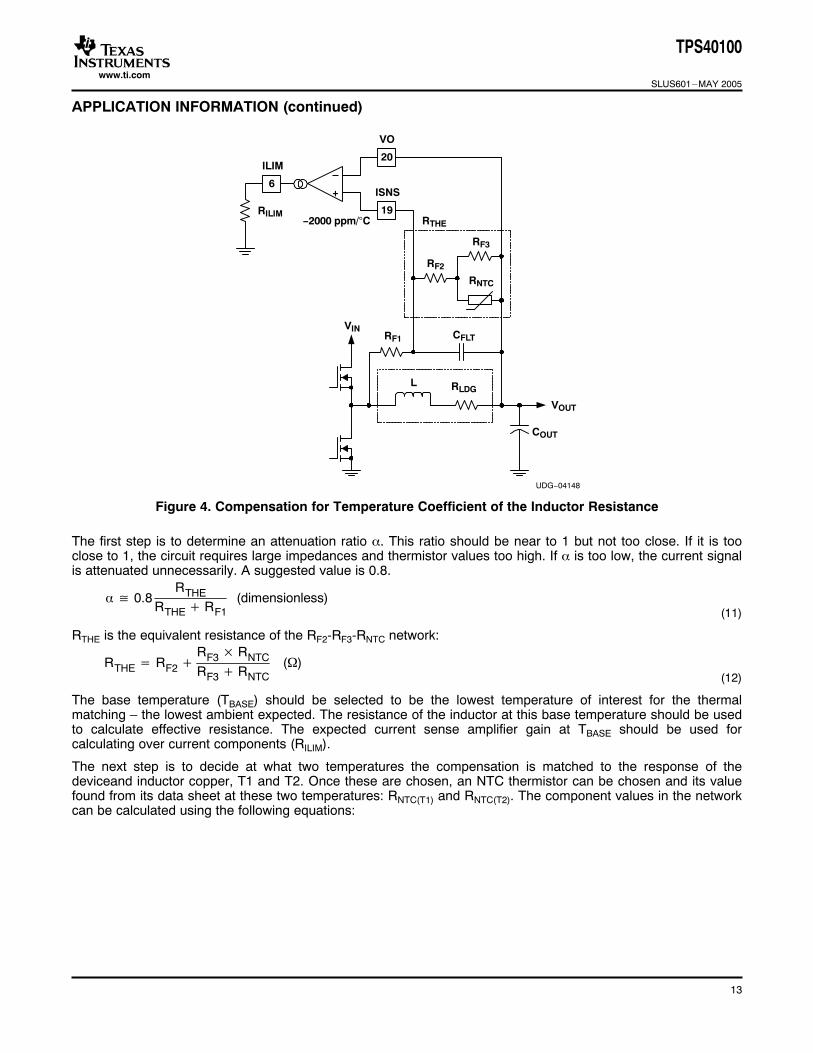
RREL(eff) is the relative effective resistance that must be compensated for when doing the compensation. Thecircuit of Figure 4 shows a method of compensating for thermal shifts in current limit. The NTC thermistor (RNTC)must be well coupled to the inductor. CFLT should be located as close to the device as possible.
12
www.ti.com
ISNS+6
ILIM
L
20
19
VO
UDG−04148
VOUT
COUT
CFLTRF1VIN
RF2
RF3
RNTC
RTHE
RLDG
RILIM−2000 ppm/°C
0.8RTHE
RTHE RF1(dimensionless)
(11)
RTHE RF2RF3 RNTCRF3 RNTC
()(12)
TPS40100
SLUS601–MAY 2005
APPLICATION INFORMATION (continued)
Figure 4. Compensation for Temperature Coefficient of the Inductor Resistance
The first step is to determine an attenuation ratio α. This ratio should be near to 1 but not too close. If it is tooclose to 1, the circuit requires large impedances and thermistor values too high. If α is too low, the current signalis attenuated unnecessarily. A suggested value is 0.8.
RTHE is the equivalent resistance of the RF2-RF3-RNTC network:
The base temperature (TBASE) should be selected to be the lowest temperature of interest for the thermalmatching – the lowest ambient expected. The resistance of the inductor at this base temperature should be usedto calculate effective resistance. The expected current sense amplifier gain at TBASE should be used forcalculating over current components (RILIM).
The next step is to decide at what two temperatures the compensation is matched to the response of thedeviceand inductor copper, T1 and T2. Once these are chosen, an NTC thermistor can be chosen and its valuefound from its data sheet at these two temperatures: RNTC(T1) and RNTC(T2). The component values in the networkcan be calculated using the following equations:
13

www.ti.com
RF1 L
RLDC(Tbase)CFLT
()
(13)
RLDC(T1) RLDC(Tbase) RREL(effT1) ()(14)
RLDC(T2) RLDC(Tbase) RREL(effT2) ()(15)
RTHE(T1) RLDC(Tbase) RF1
RLDC(T1) RLDC(Tbase)()
(16)
RTHE(T2) RLDC(Tbase) RF1
RLDC(T2) RLDC(Tbase)()
(17)
a 1RNTC(T1) RNTC(T2)RTHE(T1) RTHE(T2)
(dimensionless)(18)
b RNTC(T1) RNTC(T2) ()(19)
c RNTC(T1) RNTC(T2) (2)
(20)
RF3 b b2 4ac
2a()
(21)
RF2 RTHE(T1) RF3 RNTC(T1) RF3 RNTC(T1)
RF3 RNTC(T1)()
(22)
Establishing Current Feedback
RGM 343.443 gmCSA
2 0.01543 gmCSA 3.225 106()
(23)
TPS40100
SLUS601–MAY 2005
APPLICATION INFORMATION (continued)
where• L is the value of the output inductance (H)• CFLT is the value of the current sense filter capacitor (F)• α is the attenuation ratio chosen from Equation 11• RTHE(T1), RTHE(T2) are the equivalent resistances of the RTHE network at temperatures T1 and T2• RLDC(Tbase) is the DC resistance of the inductor at temperature TBASE in Ω
• RLDC(T1), RLDC(T2) are the inductor resistances at temperatures T1 and T2• RREL(effT1), RREL(effT2), are the relative resistances of the inductor at T1 and T2 vs. Tbase• RNCT(T1), RNTC(T2) are the effective resistance of the NTC thermistor at temperatures T1 and T2
The amount of current feedback in a given application is programmable by the user. The amount of currentfeedback used is intended to be just enough to reduce the Q of the output filter double pole. This allows designof a converter control loop that is stable for a very wide range of output capacitance. Setting the current feedbackhigher offers little real benefit and can actually degrade load transient response, as well as introduce pulseskipping in the converter. The current feedback is adjusted by setting the gain of the current sense amplifier. Theamplifier is a transconductance type and its gain is a set by connecting a resistor from the GM pin to GND:
where• RGM is the resistor that sets the gain of the amplifier (Ω)• gmCSA is the gain of the current sense amplifier (S)
The value of the sense amplifier gain should be less than 1000 µS, and more than 250 µS, with the resultinggain setting resistor greater than 50 kΩ. As a suggested starting point, set the gain of the current sense amplifierto a nominal 280 µS with RGM of 279 kΩ. This value should accommodate most applications adequately.Figure 5 shows the current sense amplifier gain setting resistance vs. the sense amplifier gain.
14

www.ti.com
75
125
275
325
175
25
225
250 400 700550 1000850
gm − Sense Amplifier Transconductance − µS
RG
M −
Gai
n S
ettin
g R
esis
tan
ce −
kΩ
Control to Output Gain of the Converter
KCO(s)VIN KPWM KFILT(s)
1 Y(s) KCS KPWM VIN(dimensionless)
(24)
RLOADRLDC RLOAD
RESR COUT s 1
LCOUTRLOADRLDCRLOAD
s2LCOUTRLOADRESRRLDCRLOADRLDCRESR
RLOAD s 1
KFILT(s)RESR COUT s 1
L COUT s2LRLOADCOUTRESRRLDCRLOAD
s 1
(26)
TPS40100
SLUS601–MAY 2005
APPLICATION INFORMATION (continued)CURRENT SENSE AMPLIFIER GAIN SETTING RESISTANCE
vsCURRENT SENSE AMPLIFIER GAIN
Figure 5.
A model that gives a good first order approximation to the control to output gain of a converter based on theTPS40100 controller is shown in Figure 6. This model can be used in conjunction with a simulator to generate acand transient response plots. The block labeled “X2” is a simple gain of 2. The amplifier gm can be a simplevoltage controlled current source with a gain equal to the selected gm for the current sense amplifier (CSA).
Analytically, the control to output gain of this model ( Figure 6) can be expressed as follows:
KFILT(s) is the output filter transfer function:
KFILT(s) =
(25)(dimensionless)
Usually, RLDC << RLOAD and the following approximation holds:
Y(s) is the current signal transfer function and assumes that the inductor intrinsic time constant is matched to thecurrent sense filter network time constant.
15

www.ti.com
Y(s) 1 KFILT(s)
LRLDC
s 1(dimensionless)
(27)
KCS gmCSA 20 k (dimensionless) (28)
++
L
ISNS
+
X2+
FBCOMP
690 mV
1 V AC
gmCSA
COUTCFLT
R2
RLOAD
R1
RBIAS
UDG−04149
RESR
C2
C1
RFLT
RLDC
VIN
VO
REA
20 kΩ
VOUT
VX
Compensating the Loop (Type II)
fC fSW5
(Hz)(29)
TPS40100
SLUS601–MAY 2005
APPLICATION INFORMATION (continued)
KCS is the gain of the current sense amplifier in the current feedback loop:
where (for Equation 24 through Equation 28)• VIN is the input voltage (V)• KPWM is the gain of the pulse width modulator and is equal to 2• RLOAD is the equivalent load resistance (Ω)• RLDC is the DC inductor resistance (Ω)• L is the output filter inductance (H)• COUT is the output filter capacitance (F)• RESR is the equivalent series resistance of the output filter capacitor (Ω)• gmCSA is the gain of the current sense amplifier (S)• 20 kΩ is the impedance the current sense amplifier works against (from block diagram)
A computer aided math tool is highly recommended for use in evaluating these equations.
Figure 6. Averaged Model for a Converter Based on the TPS40100
The first step is to select a target loop crossover frequency. Choosing the crossover frequency too highcontributes to making the converter pulse skip. A balance of crossover frequency and amount of currentfeedback must be maintained to avoid pulse skipping. A suggested maximum loop crossover frequency is onefifth-of the switching frequency.
where• fC is the loop crossover frequency• fSW is the switching frequency
16

www.ti.com
KCOMP(co) 1
KCO(fc)(Hz)
(30)
f − Frequency − kHz
Gai
n −
dB
fZ fC fP
KCOMP(co)
R2 KLF R1 () (31)
TPS40100
SLUS601–MAY 2005
APPLICATION INFORMATION (continued)
Using either the analytical model or the simulated model, determine the control to output gain at the chosen loopcrossover frequency. The gain of the compensator is the reciprocal of this gain:
where• KCOMP(CO) is the required compensator gain at the crossover frequency• KCO(fC) is the value of the control to output transfer function at the crossover frequency
If simulating the response using the model, the control to output gain is VX/VOUT. Sweep the AC voltage sourceover the range of interest and plot VX/VOUT.
Depending on the chosen loop crossover frequency and the characteristics of the output capacitor, either a TypeII or a Type III compensator could be required. If the output capacitance has sufficient ESR, phase shift from theESR zero may by used to eliminate the need for a Type III compensator. The model in Figure 6 uses a Type IIcompensator. In this case the compensator response looks like Figure 7.
COMPENSATOR GAINvs
FREQUENCY
Figure 7.
First select R1. The choice is somewhat arbitrary but affects the rest of the components once chosen. Thesuggested value is 10 kΩ.
R2 is found from the gain required from the compensator at the crossover frequency.
It is generally recommended to place the pole frequency one decade above the crossover frequency and thezero frequency one decade below the crossover frequency.
17

www.ti.com
fP fC 10 12 R2 C1
(Hz)(32)
fZ fC10
12 R2 C2
(Hz)(33)
Compensating the Loop (Type III)
+
VX
COMP
Error Amplifier
FB
UDG−04143
R2 R1
RBIAS
C2
C1 R3C3
f − Frequency − kHz
Gai
n −
dB
fZ fZ3 fP3
KHF
KCOMP(co)
KLF
fC fP
TPS40100
SLUS601–MAY 2005
APPLICATION INFORMATION (continued)
If the output capacitor does not have sufficient ESR to use the phase shift from the ESR zero, a Type IIIcompensator is required. This is the case for most designs with ceramic output capacitors only. A series R-Ccircuit is added in parallel to R1 as shown in Figure 8.
This is the same compensator as in Figure 6 except for the addition of C3 and R3. A typical response of thiscircuit is shown in Figure 9.
COMPENSATOR GAINvs
FREQUENCY
Figure 9. Figure 8. Type III Compensator Schematic
The reason for using the Type III compensator is to take advantage of the phase lead associated with theupward slope of the gain between fZ3 and fP3. The crossover frequency should be located between these twofrequencies. The amount of phase lead generated is dependent on the separation of the fZ3 and fP3. In general, iffZ3 is one half of fC and fP3 is twice fC, the amount of phase lead at fC generated is sufficient for most applications.Certainly more or less may be used depending on the situation.
As an example of selecting the extra required extra phase lead, suppose that the control to output gain phaseevaluates to -145° at fC. The Type II compensator has approximately 11.5° of phase lag at fC due to the originpole, the zero at fC/10 and the pole at 10xfC. This would give only 23.5° of phase margin, which while stable isnot ideal. Placing fZ3 and fP3 at one half and twice the crossover frequency respectively adds approximately 36°of phase lead at fC for a new phase margin of 59.5°.
To calculate the values for this type of compensator, first select R1. Again the choice is somewhat arbitrary. 10kΩ is a suggested value.
18

www.ti.com
K3 tanLEAD tanLEAD
1 (dimensionless)(34)
fZ3 fCK3
(Hz)(35)
fP3 fC K3 (Hz) (36)
KLF KCOMP(co)
K3(dimensionless)
(37)
R2 KLF R1 () (38)
KHF KCOMP(co) K3 (dimensionless)(39)
R3 R1 R2
KHF R1 R2()
(40)
C3 1
2 R3 fP3(F)
(41)
TPS40100
SLUS601–MAY 2005
APPLICATION INFORMATION (continued)
Select the required extra phase lead beyond the Type II compensation to obtain the required phase margin andcalculate the required multiple for the additional pole and zero:
where• ΘLEAD is the required extra phase lead to be generated by the addition of the extra pole and zero• K3 is the multiplier applied to fC to get the new pole and zero locations
The locations of fZ3 and fP3 are:
where• K3 is the multiplier applied to fC to get the new pole and zero locations• fZ3 is the zero created by the addition of R3 and C3
• fP3 is the pole created by the addition of R3 and C3
The required gain, KCOMP(co), from the compensator at fC, is the same as for the Type II compensation, found inEquation 30. The gain KLF (see Figure 9) is found by:
R2 can then be found:
The high-frequency gain is:
Now:
The remaining pole and zero are located a decade above and below fC as before. Equation 31 and Equation 32can be used to solve for C1 and C2 as before.
19
www.ti.com
Establishing Tracking and Designing a Tracking Control Loop
+
COMPFB
12
20
4
690 mV
+3
TRKOUT
To PWM
A
A
VO
TRKIN
RBIAS
UDG−04145
R2
R1
C2
C1
R3
C3
C5C4
R4
VOUT
VIN
R5
R6D1
R4 VHTRKOUT(min) VDIODE VFB
VFB
R1 RBIASR1 RBIAS
(42)
dVOUTdVTRKOUT
R1R4
(dimensionless)(43)
TPS40100
SLUS601–MAY 2005
APPLICATION INFORMATION (continued)
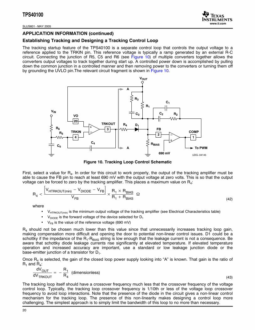
The tracking startup feature of the TPS40100 is a separate control loop that controls the output voltage to areference applied to the TRKIN pin. This reference voltage is typically a ramp generated by an external R-Ccircuit. Connecting the junction of R5, C5 and R6 (see Figure 10) of multiple converters together allows theconverters output voltages to track together during start up. A controlled power down is accomplished by pullingdown the common junction in a controlled manner and then removing power to the converters or turning them offby grounding the UVLO pin.The relevant circuit fragment is shown in Figure 10.
Figure 10. Tracking Loop Control Schematic
First, select a value for R4. In order for this circuit to work properly, the output of the tracking amplifier must beable to cause the FB pin to reach at least 690 mV with the output voltage at zero volts. This is so that the outputvoltage can be forced to zero by the tracking amplifier. This places a maximum value on R4:
where• VHTRKOUT(min) is the minimum output voltage of the tracking amplifier (see Electrical Characteristics table)• VDIODE is the forward voltage of the device selected for D1
• VFB is the value of the reference voltage (690 mV)
R4 should not be chosen much lower than this value since that unnecessarily increases tracking loop gain,making compensation more difficult and opening the door to potential non-linear control issues. D1 could be aschottky if the impedance of the R1-RBIAS string is low enough that the leakage current is not a consequence. Beaware that schottky diode leakage currents rise significantly at elevated temperature. If elevated temperatureoperation and increased accuracy are important, use a standard or low leakage junction diode or thebase-emitter junction of a transistor for D1.
Once R4 is selected, the gain of the closed loop power supply looking into “A” is known. That gain is the ratio ofR1 and R4:
The tracking loop itself should have a crossover frequency much less that the crossover frequency of the voltagecontrol loop. Typically, the tracking loop crossover frequency is 1/10th or less of the voltage loop crossoverfrequency to avoid loop interactions. Note that the presence of the diode in the circuit gives a non-linear controlmechanism for the tracking loop. The presence of this non-linearity makes designing a control loop morechallenging. The simplest approach is to simply limit the bandwidth of this loop to no more than necessary.
20

www.ti.com
R5 C4 R4
2 R1 fcTRK(s)
(44)
t − Time − 1 ms/div
(200 mV/div)
tTRK R6 C5 ln1 VOUTVIN (s)
(45)
TPS40100
SLUS601–MAY 2005
APPLICATION INFORMATION (continued)
Knowing the gain of the voltage loop looking into R4 and the desired tracking loop crossover frequency, R5 andC4 can be found:
where• fCTRK is the desired tracking loop crossover frequency
The actual values of R5 and C4 are a balance between impedance level and component size. Any of a range ofvalues is applicable. In general, R5 should be no more than 20% of R6, and less than 10 kΩ. If this is done, thenR6 can safely be ignored for purposes of tracking loop gain calculations. For general usage, R6 should probablybe between 100 kΩ and 500 kΩ.
If an overshoot bump is present on the output at the beginning a tracking controlled startup, the tracking loopbandwidth is likely too high. Reducing the bandwidth helps reduce the initial overshoot. See Figure 11 andFigure 12.
Figure 11. Excessive Tracking Loop Bandwidth Figure 12. Limited Tracking Loop Bandwidth
The tracking ramp time is the time required for C5 to charge to the same voltage as the output voltage of theconverter.
where• VOUT is the output voltage of the converter• VIN is the voltage applied to the top of R6
• tTRK is the desired tracking ramp time
With these equations, it is possible to design the tracking loop so that the impedance level of the loop and thecomponent size are balanced for the particular application. Note that higher impedances make the loop moresusceptible to noise issues while lower impedances require increased capacitor size.
Figure 13 shows the spice model for the voltage loop expanded for use with the tracking loop.
21

www.ti.com
+
+
C4
++
L
ISNS
+
X2+
RLOAD
RCESR
COUT
RLDC
CSFLTRSFLT
gmCSA
REA20 kΩ
RBIAS
R4R5
R1
R3 C3
C1
C2R2
VIN
UDG−04147
VOUT
VX
Programming Soft-Start Time
CSS TSS20 AVFB
F(46)
TPS40100
SLUS601–MAY 2005
APPLICATION INFORMATION (continued)
Figure 13. AC Behavioral Model for Tracking Control Loop
To use the model, the AC voltage source is swept over the frequency range of interest. The open loop acresponse is VX/VOUT.
The soft-start time of the TPS40100 is fully user programmable by selecting a single capacitor. The SS pinsources 20 µA to charge this capacitor. The actual output ramp-up time is the amount of time that it takes for the20 µA to charge the capacitor through a 690 mV range. There is some initial lag due to an offset from the actualSS pin voltage to the voltage applied to the error amplifier. See Figure 15. The soft-start is done in a closed loopfashion, meaning that the error amplifier controls the output voltage at all times during the soft start period andthe feedback loop is never open as occurs in duty cycle limit soft-start schemes. The error amplifier has twonon-inverting inputs, one connected to the 690 mV reference voltage, and one connected to the offset SS pinvoltage. The lower of these two voltages is what the error amplifier controls the FB pin to. As the voltage on theSS pin ramps up past approximately 1.04 V (resulting in 690 mV at the SS “+” input – See Figure 15), the 690mV reference voltage becomes the dominant input and the converter has reached its final regulation voltage.
The capacitor required for a given soft-start ramp time for the output voltage is given by:
where• TSS is the desired soft-start ramp time (s)• CSS is the required capacitance on the SS pin (F)• VFB is the reference voltage feedback loop (690 mV)
22

www.ti.com
1
10
2
COMP
FB
SS
++
+
690 mV
350 mV
COMP
CHARGEFrom UVLO circuits,Fault controller
Error Amplifier
5 µA
20 µA
CSS
UDG−04138
Tss
Tss Delay
1.04 V
0.35 V
UVLO
SS
VOUT
PDG
3.5 V
4.8 V
(Internal Logic State)
Interaction Between Soft-Start and Tracking Startup
TPS40100
SLUS601–MAY 2005
APPLICATION INFORMATION (continued)
Figure 14. Error Amplifier and Soft-Start Functional Diagram
Figure 15. Relationship Between UVLO (Internal Logic State), SS, VOUT and PGD at Startup
Since the TPS40100 provides two means of controlling the startup (closed loop soft-start and tracking) care mustbe taken to ensure that the two methods do not interfere with each other. The two methods should not beallowed to try and control the output at the same time. If tracking is to be used, the reference input to the trackingamplifier (TRKIN) should be held low until soft-start completes, or the voltage at the SS pin is at least above 1.04V. This ensures that the soft-start circuit is not trying to control the startup at the same time as tracking circuit. Ifit is desired to have soft-start control the startup, then there are two options:
23

www.ti.com
Overcurrent Protection
RILIM VILIM
gmCSA RLDC IOC
(47)
tOC RILIM CILIM ln1 1n (s)
(48)
TPS40100
SLUS601–MAY 2005
APPLICATION INFORMATION (continued)
• Disconnect the tracking amplifier output from the FB node (this is the recommended solution. The trackingamplifier can then be used for other system purposes if desired)
• Maintain the tracking amplifier output connection to the FB circuit - the reference to the tracking amplifiershould be tied to VDD pin in this case. This places the tracking amplifier output (TRKOUT) in a low statecontinuously and therefore removes any influence the tracking circuit has on the converter startup.
Additionally, when tracking is allowed to control the startup, soft-start should not be set to an arbitrarily shorttime. This causes the output voltage to bump up when power is applied to the converter as soft-start ramps upquickly and the tracking loop (which is necessarily low bandwidth) cannot respond fast enough to control theoutput to zero voltage. In other words, the soft start ramp rate must be within the capability of the tracking loop tooverride.
Overcurrent characteristics are determined by connecting a parallel R-C network from the ILIM pin to GND. TheILIM pin sources a current that is proportional to the current sense amplifier transconductance and the voltagebetween ISNS and VO. This current produces a voltage on the R-C network at ILIM. If the voltage at the ILIM pinreaches 1.48 V, an overcurrent condition is declared and the outputs stop switching for a period of time. Thistime period is determined by the time is takes to discharge the soft-start capacitor with a controlled current sink.To set the overcurrent level:
where• VILIM is the overcurrent comparator threshold (1.48 V typically)• IOC is the overcurrent level to be set• gmCSA is the transconductance of the current sensing amplifier• RLDC is the equivalent series resistance of the inductor (or the sense resistor value)• RILIM is the value of the resistor from ILIM to GND
The response time of the overcurrent circuit is determined by the R-C time constant at the ILIM pin and the levelof the overcurrent. The response time is given by:
where• tOC is the response time before declaring an overcurrent• RILIM (Ω) and CILIM (F) are the components connected to the ILIM pin• n is the multiplier of the overcurrent. If the overcurrent is 2 times the programmed level, then n is 2.
By suitable manipulation of the time constant at ILIM, the overcurrent response can be tailored to ride out shortterm transients and still provide protection for overloads and short circuits. The gm of the current sense amplifierhas a temperature coefficient of approximately -2000 ppm/°C. This is to help offset the temperature coefficient ofresistance of the copper in the inductor, about +4000 ppm/°C. The net is a +2000 ppm/°C temperaturecoefficient. So, for a 100°C increase in temperature, the overcurrent threshold decreases by 20%, assuminggood thermal coupling between the controller and the inductor. Temperature compensation can be done asdescribed earlier if desired.
When an overcurrent condition is declared, the controller stops switching and turns off both the high-sideMOSFET and the low-side MOSFET. The soft-start capacitor is then discharged at 25% of the charge rate duringan overcurrent condition and the converter remains idle until the soft start pin reaches 200 mV, at which point thesoft-start circuit starts charging again and the converter attempts to restart. In normal operation, the soft-startcapacitor is charged to approximately 3.5 V when an initial fault is applied to the output. This means that theminimum time before the first restart attempt is:
24

www.ti.com
tRESTART 3.3 CSSISSDIS
(s)(49)
UVLO Programming
5
UVLO 1.33 V +
TPS40100
UDG−04139
10 µA
R1
R2
UVLO
R1 VHYSTIUVLO
(50)
R2 VUVLO R1
VON VUVLO R1 IUVLO
(51)
TPS40100
SLUS601–MAY 2005
APPLICATION INFORMATION (continued)
where• tRESTART is the initial restart time (s)• CSS is soft start capacitance (F)• ISSDIS is the soft start discharge current – 5 µA
If the output fault is persistent, and an overcurrent is declared on the restart, both of the MOSFETs are turned offand the soft-start capacitor continues to charge to 3.5 V and then discharge to 200 mV before another restart isattempted.
The TPS40100 provides the user with programmable UVLO level and programmable hysteresis. The UVLOdetection circuit schematic is described in Figure 16 from a functional perspective.
Figure 16. UVLO Circuit Functional Diagram
To program this circuit, first select the amount of hysteresis (the difference between the startup voltage and theshutdown voltage) desired:
Then select the turn-on voltage and solve for R2.
where• VHYST is the desired level of hysteresis in the programmable UVLO circuit• IUVLO is the undervoltage lockout circuit hysteresis current (10 µA typ)• VUVLO is the UVLO comparator threshold voltage (1.33 V typ)
25

www.ti.com
Voltage Margining
Synchronization
Power Good Indication
TPS40100
SLUS601–MAY 2005
APPLICATION INFORMATION (continued)
The TPS40100 allows the user to make the output voltage temporarily be 3% above or below the nominal output,or 5% above or below the nominal output. This is accomplished by connecting the MGU or MGD pins to GNDdirectly or through a resistance. See Table 1.
Table 1. Output Voltage Margining States
RESISTANCE TO GND (kΩ)OUTPUT VOLTAGE
RMGU RMGD
OPEN OPEN Nominal
< 10 OPEN + 5%
OPEN < 10 -5%
25 to 37 OPEN +3%
OPEN 25 to 37 -3%
There are some important considerations when adjusting the output voltage.• Only one of these pins should be anything other than an open circuit at any given time. States not listed in
the table are invalid states and the behavior of the circuit may be erratic if this is tried.• When changing the output voltage using the margin pins, it is very important to let the margin transition
complete before altering the state of the margin pins again.• Do not use mechanical means (switches, non-wetted relay contacts, etc) to alter the margining state. The
contact bounce causes erratic behavior.
The TPS40100 may be synchronized to an external clock source that is faster than the free running frequency ofthe circuit. The SYNC pin is a rising edge sensitive trigger to the oscillator that causes the current cycle toterminate and starts the next switching cycle. It is recommended that the synchronization frequency be no morethan 120% of the free running frequency. Following this guideline leads to fewer noise and jitter problems withthe pulse width modulator in the device. The circuit can be synchronized to higher multiples of the free runningfrequency, but be aware that this results in a proportional decrease in the amplitude of the ramp from theoscillator applied to the PWM, leading to increased noise sensitivity and increased PWM gain, possibly affectingcontrol loop stability.
The pulse applied to the SYNC pin can be any duty ratio as long as the pulse either high or low is at least 100 nswide. Levels are logic compatible with any voltage under 1 V considered a low and any voltage over 2 Vconsidered a high.
The PGD pin is an open drain output that actively pulls to GND if any of the following conditions are met(assuming that the input voltage is above 4.5V)• Soft-start is active (VSS < 3.5 V)• Tracking is active (VTRKOUT > 0.7 V)• VFB < 0.61 V• VFB > 0.77 V• VUVLO < 1.33 V• Overcurrent condition exists• Die temperature is greater than 165°C
A short filter (20 µs) must be overcome before PGD pulls to GND from a high state to allow for short transientconditions and noise and not indicate a power NOT good condition.
The PGD pin attempts to pull low in the absence of input power. If the VDD pin is open circuited, the voltage onPGD typically behaves as shown in Figure 17.
26

www.ti.com
2.5
2.0
1.5
1.0
0.5
00 1 2 3 4 5
IPGD − Powergood Current − mA
VP
GD
− P
ow
erg
oo
d V
olta
ge −
V
VVDD = 0 V
Pre-Bias Operation
Remote Sense
TPS40100
SLUS601–MAY 2005
POWERGOOD VOLTAGEvs
POWERGOOD CURRENT
Figure 17.
Some applications require that the converter not sink current during startup if a pre-existing voltage exists at theoutput. Since synchronous buck converters inherently sink current some method of overcoming this characteristicmust be employed. Applications that require this operation are typically power rails for a multiple supplyprocessor or ASIC. The method used in this controller, is to not allow the low side or rectifier FET to turn on untilthere the output voltage commanded by the start up ramp is higher than the pre-existing output voltage. This isdetected by monitoring the internal pulse width modulator (PWM) for its first output pulse. Since this controlleruses a closed loop startup, the first output pulse from the PWM does not occur until the output voltage iscommanded to be higher than the pre-existing voltage. This effectively limits the controller to sourcing currentonly during the startup sequence. If the pre-existing voltage is higher that the intended regulation point for theoutput of the converter, the converter starts and sinks current when the soft-start time has completed.
The TPS 40100 is capable of remotely sensing the load voltage to improve load regulation. This is accomplishedby connecting the GND pin of the device and the feedback voltage divider as near to the load as possible.
CAUTION:
Long distance runs for the GND pin will cause erratic controller behavior.
This begins to appear as increased pulse width jitter. As a starting point, the GND pin connection should be nofurther than six inches from the PGND connection. The actual distance that starts causing erratic behavior isapplication and layout dependent and must be evaluated on an individual basis. If the controller exhibits outputpulse jitter in excess of 25 ns and the GND pin is tied to the load ground, connecting the GND pin closer to thePGND pin (and thereby sacrificing some load regulation) may improve performance. In either case, connectingthe feedback voltage divider at the point of load should not cause any problems. For layout, the voltage dividercomponents should be close to the device and a trace can be run from there to the load point.
27

www.ti.com
Application Schematics
27 kΩ
27 kΩ
14.3 kΩ
30 kΩ
4.99 kΩ
200 kΩ100 kΩ
40.2 kΩ 13.7 kΩ
158 kΩ
162 kΩ 1 µF
270 kΩ
1 µF
10 Ω
VOUT1.2 V15 A
470 µFPanasonic
1.0 µHCOEV
DXM1306−1R01.7 mΩ (typ)
5.9 kΩ
10 kΩ
VOUT
UDG−04140
1 µF
TPS40100
1
3
18
16
2
4
17
15
5
6
14
13
24 2223 21 20 19
7 98 10 11 12
COMP
FB
TRKOUT
TRKIN
UVLO
ILIM
MG
U
MG
D
SY
NC
PG
VO
ISN
S
RT
BIA
S
GN
D
SS
GM
PG
ND
VDD
SW
HDRV
BST
5VBP
LDRV
150 nF
100 pF
BAT54
100 nF
100 nF
12 V
300 pF
MMBD1501A
12 VSi73444DP
Si7868DP EEF−SEOD471R
10 nF(if required)
Connect at load
47 nF
Margin up 3%
Margin down 3% Power Good Indication
BAT54S(if required)
RemoteGND SenseConnect atLoad
2
1 1
1
2 Open switch after input power is stable and SS capacitor had finished charging.
22 µF TDK C4532X7R1C226M
2N7002
2N7002
47 pF
3.3 V to 5 V logic supply or 5VBP pin
TPS40100
SLUS601–MAY 2005
Figure 18. 300-kHz, 12-V to 1.2-V Converter With Tracking Startup Capability and Remote Sensing
28
www.ti.com
6.2 kΩ
15 kΩ
4.99 kΩ
200 kΩ100 kΩ
1 µF 2.67 kΩ
158 kΩ
120 kΩ 1 µF 270 kΩ
1 µF
22 µF TDK C4532X7R1C226M
100 µF TDK C3225X5ROJ107M
VOUT3.3 V15 A
1.0 µHCOEV
DXM1306−1R01.7 mΩ (typ)
5.9 kΩ
10 kΩ
VOUT
UDG−04141
47 pF
TPS40100
1
3
18
16
2
4
17
15
5
6
14
13
24 2223 21 20 19
7 98 10 11 12
COMP
FB
TRKOUT
TRKIN
UVLO
ILIM
MG
U
MG
D
SY
NC
PG
VO
ISN
S
RT
BIA
S
GN
D
SS
GM
PG
ND
VDD
SW
HDRV
BST
5VBP
LDRV
150 nF
100 pF
BAT54
100 nF
100 nF
12 V
3.9 nF
47 nFMMBD1501A
12 VSi7344DP
Si7868DP
Connect at load
2N7002
Margin up 5%
2N7002
Margin down 5% Power Good Indication
330 pF
1
2
3
3 Open switch after input power is stable and SS capacitor had finished charging.
1
2
1
2 2
3.32 kΩ
40.2 kΩ
3.3 V to 5 V logic supply or 5VBP pin
TPS40100
SLUS601–MAY 2005
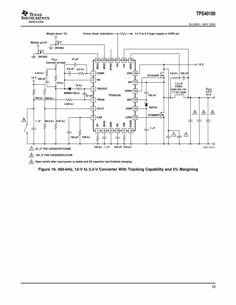
Figure 19. 400-kHz, 12-V to 3.3-V Converter With Tracking Capability and 5% Margining
29
www.ti.com
TPS40100
1
3
18
16
2
4
17
15
5
6
14
13
24 2223 21 20 19
7 98 10 11 12
COMP
FB
TRKOUT
TRKIN
UVLO
ILIM
MG
U
MG
D
SY
NC
PG
VO
ISN
S
RT
BIA
S
GN
D
SS
GM
PG
ND
VDD
SW
HDRV
BST
5VBP
LDRV
150 nF
100 pF
BAT54
100 nF
100 nF
12 V
300 pF
47 pF
12 V
Si73444DP
Si7868DP
NC NC NC NC
NC
NC
1
11
10 kΩ
1 µHCOEV
DXM1306−1R01.7 mΩ (typ)
VOUT1.2 V15 A
22 µF TDK C4532X7R1C226M
UDG−05063
470 µFPanasonic
EEF−SEOD471R
14.3 kΩ
200 kΩ
40.2 kΩ 13.7 kΩ
158 kΩ
187 kΩ 1 µF
1 µF
5.9 kΩ
270 kΩ
TPS40100
SLUS601–MAY 2005
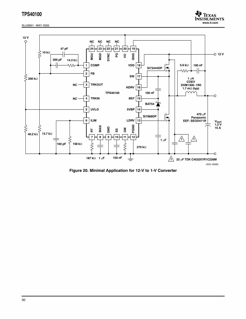
Figure 20. Minimal Application for 12-V to 1-V Converter
30

www.ti.com
TPS40100
1
3
18
16
2
4
17
15
5
6
14
13
24 2223 21 20 19
7 98 10 11 12
COMP
FB
TRKOUT
TRKIN
UVLO
ILIM
MG
U
MG
D
SY
NC
PG
VO
ISN
S
RT
BIA
S
GN
D
SS
GM
PG
ND
VDD
SW
HDRV
BST
5VBP
LDRV
150 nF
100 pF
BAT54
100 nF
100 nF
12 V
300 pF
47 pF
12 V
Si73444DP
Si7868DP
NC NC
NC
NC
TPS40100
1
3
18
16
2
4
17
15
5
6
14
13
24 2223 21 20 19
7 98 10 11 12
COMP
FB
TRKOUT
TRKIN
UVLO
ILIM
MG
U
MG
D
SY
NC
PG
VO
ISN
S
RT
BIA
S
GN
D
SS
GM
PG
ND
VDD
SW
HDRV
BST
5VBP
LDRV
150 nF
100 pF
BAT54
100 nF
100 nF
12 V
3.9 nF
470 pF
12 V
Si7344DP
Si7868DP
330 pF
NC
NC
NC NC
External 5 V
1
1 1
2
2 2 2
1 1
10 kΩ
14.3 kΩ
200 kΩ
40.2 kΩ 13.7 kΩ
187 kΩ
158 kΩ
1 µF
270 kΩ
5.9 kΩ
1 µHCOEV
DXM1306−1R01.7 mΩ (typ)
1 µF
470 µFPanasonicEEF−SEOD471R
VOUT1.2 V15 A
10 kΩ
3.32 kΩ6.2 kΩ
200 kΩ
2.67 kΩ40.2 kΩ
10 kΩ
120 kΩ
1 µF
270 kΩ1 µF
1 µHCOEV
DZM1306−1R3 mΩ (typ)
5.9 kΩ
VOUT3.3 V15 A
100 µF TDK C3225X5ROJ107M
22 µF TDK C4532X7R1C226M
ExternalClock50%Duty
PowerGood
UDG−05064
158 kΩ
TPS40100
SLUS601–MAY 2005
Figure 21. Sequenced Supplies, With Oscillators 180 Degrees Out of Phase
31

www.ti.com
1 µHCOEV
DZM1306−1R3 mΩ (typ)
VOUT3.3 V15 A
22 µF TDK C4532X7R1C226M UDG−05066
470 µFPanasonic
EEF−SEOD471R
TPS40100
1
3
18
16
2
4
17
15
5
6
14
13
24 2223 21 20 19
7 98 10 11 12
COMP
FB
TRKOUT
TRKIN
UVLO
ILIM
MG
U
MG
D
SY
NC
PG
VO
ISN
S
RT
BIA
S
GN
D
SS
GM
PG
ND
VDD
SW
HDRV
BST
5VBP
LDRV
150 nF
100 pF
BAT54
100 nF
100 nF
12 V
300 pF
47 pF12 V
Si73444DP
Si7868DP
NC NC
TPS40100
1
3
18
16
2
4
17
15
5
6
14
13
24 2223 21 20 19
7 98 10 11 12
COMP
FB
TRKOUT
TRKIN
UVLO
ILIM
MG
U
MG
D
SY
NC
PG
VO
ISN
S
RT
BIA
S
GN
D
SS
GM
PG
ND
VDD
SW
HDRV
BST
5VBP
LDRV
150 nF
100 pF
BAT54
100 nF
100 nF
12 V
3.9 nF
470 pF
12 V
Si7344DP
Si7868DP
330 pF
NC NC
External5V
PowerGood
External Clock,50% duty
47 nFMMBD1501A
47 nFMMBD1501A
12 V
3 Open switch after input power is stable and SS capacitor has finished charging.
3
1
2
1 1
2 2 2
1 1
VOUT1.2 V15 A
200 kΩ
40.2 kΩ
13.7 kΩ158 kΩ
10 kΩ
14.3 kΩ
187 kΩ
1 µF
5.9 kΩ
30 kΩ
4.99 kΩ
270 kΩ
1 µF
10 kΩ
470 µFPanasonicEEF−SEOD471R
5.9 kΩ
1 µF
100 µF TDK C3225X5ROJ107M
40.2 kΩ 2.67 kΩ
158 kΩ
120 kΩ
270 kΩ
1 µF
4.99 kΩ
15 kΩ
200 kΩ
3.32 kΩ 10 kΩ
6.2 kΩ
47 kΩ
2.2 µF
TPS40100
SLUS601–MAY 2005
Figure 22. Tracking Supplies
32

PACKAGE OPTION ADDENDUM
www.ti.com 13-Aug-2021
Addendum-Page 1
PACKAGING INFORMATION
Orderable Device Status(1)
Package Type PackageDrawing
Pins PackageQty
Eco Plan(2)
Lead finish/Ball material
(6)
MSL Peak Temp(3)
Op Temp (°C) Device Marking(4/5)
Samples
TPS40100RGER ACTIVE VQFN RGE 24 3000 RoHS & Green NIPDAU Level-2-260C-1 YEAR -40 to 85 TPS40100
TPS40100RGET ACTIVE VQFN RGE 24 250 RoHS & Green NIPDAU Level-2-260C-1 YEAR -40 to 85 TPS40100
TPS40100RGETG4 ACTIVE VQFN RGE 24 250 RoHS & Green NIPDAU Level-2-260C-1 YEAR -40 to 85 TPS40100
(1) The marketing status values are defined as follows:ACTIVE: Product device recommended for new designs.LIFEBUY: TI has announced that the device will be discontinued, and a lifetime-buy period is in effect.NRND: Not recommended for new designs. Device is in production to support existing customers, but TI does not recommend using this part in a new design.PREVIEW: Device has been announced but is not in production. Samples may or may not be available.OBSOLETE: TI has discontinued the production of the device.
(2) RoHS: TI defines "RoHS" to mean semiconductor products that are compliant with the current EU RoHS requirements for all 10 RoHS substances, including the requirement that RoHS substancedo not exceed 0.1% by weight in homogeneous materials. Where designed to be soldered at high temperatures, "RoHS" products are suitable for use in specified lead-free processes. TI mayreference these types of products as "Pb-Free".RoHS Exempt: TI defines "RoHS Exempt" to mean products that contain lead but are compliant with EU RoHS pursuant to a specific EU RoHS exemption.Green: TI defines "Green" to mean the content of Chlorine (Cl) and Bromine (Br) based flame retardants meet JS709B low halogen requirements of <=1000ppm threshold. Antimony trioxide basedflame retardants must also meet the <=1000ppm threshold requirement.
(3) MSL, Peak Temp. - The Moisture Sensitivity Level rating according to the JEDEC industry standard classifications, and peak solder temperature.
(4) There may be additional marking, which relates to the logo, the lot trace code information, or the environmental category on the device.
(5) Multiple Device Markings will be inside parentheses. Only one Device Marking contained in parentheses and separated by a "~" will appear on a device. If a line is indented then it is a continuationof the previous line and the two combined represent the entire Device Marking for that device.
(6) Lead finish/Ball material - Orderable Devices may have multiple material finish options. Finish options are separated by a vertical ruled line. Lead finish/Ball material values may wrap to twolines if the finish value exceeds the maximum column width.
Important Information and Disclaimer:The information provided on this page represents TI's knowledge and belief as of the date that it is provided. TI bases its knowledge and belief on informationprovided by third parties, and makes no representation or warranty as to the accuracy of such information. Efforts are underway to better integrate information from third parties. TI has taken andcontinues to take reasonable steps to provide representative and accurate information but may not have conducted destructive testing or chemical analysis on incoming materials and chemicals.TI and TI suppliers consider certain information to be proprietary, and thus CAS numbers and other limited information may not be available for release.

PACKAGE OPTION ADDENDUM
www.ti.com 13-Aug-2021
Addendum-Page 2
In no event shall TI's liability arising out of such information exceed the total purchase price of the TI part(s) at issue in this document sold by TI to Customer on an annual basis.

TAPE AND REEL INFORMATION
*All dimensions are nominal
Device PackageType
PackageDrawing
Pins SPQ ReelDiameter
(mm)
ReelWidth
W1 (mm)
A0(mm)
B0(mm)
K0(mm)
P1(mm)
W(mm)
Pin1Quadrant
TPS40100RGER VQFN RGE 24 3000 330.0 12.4 4.25 4.25 1.15 8.0 12.0 Q2
TPS40100RGET VQFN RGE 24 250 180.0 12.4 4.25 4.25 1.15 8.0 12.0 Q2
TPS40100RGET VQFN RGE 24 250 180.0 12.4 4.3 4.3 1.1 8.0 12.0 Q2
PACKAGE MATERIALS INFORMATION
www.ti.com 2-Dec-2018
Pack Materials-Page 1

*All dimensions are nominal
Device Package Type Package Drawing Pins SPQ Length (mm) Width (mm) Height (mm)
TPS40100RGER VQFN RGE 24 3000 367.0 367.0 35.0
TPS40100RGET VQFN RGE 24 250 210.0 185.0 35.0
TPS40100RGET VQFN RGE 24 250 195.0 200.0 45.0
PACKAGE MATERIALS INFORMATION
www.ti.com 2-Dec-2018
Pack Materials-Page 2

GENERIC PACKAGE VIEW
Images above are just a representation of the package family, actual package may vary.Refer to the product data sheet for package details.
RGE 24 VQFN - 1 mm max heightPLASTIC QUAD FLATPACK - NO LEAD
4204104/H

www.ti.com
PACKAGE OUTLINE
C
SEE TERMINALDETAIL
24X 0.30.2
2.45 0.1
24X 0.50.3
1 MAX
(0.2) TYP
0.050.00
20X 0.5
2X2.5
2X 2.5
A 4.13.9
B
4.13.9
0.30.2
0.50.3
VQFN - 1 mm max heightRGE0024BPLASTIC QUAD FLATPACK - NO LEAD
4219013/A 05/2017
PIN 1 INDEX AREA
0.08 C
SEATING PLANE
1
6 13
18
7 12
24 19
(OPTIONAL)PIN 1 ID
0.1 C A B0.05
EXPOSEDTHERMAL PAD
25 SYMM
SYMM
NOTES: 1. All linear dimensions are in millimeters. Any dimensions in parenthesis are for reference only. Dimensioning and tolerancing per ASME Y14.5M. 2. This drawing is subject to change without notice. 3. The package thermal pad must be soldered to the printed circuit board for thermal and mechanical performance.
SCALE 3.000
DETAILOPTIONAL TERMINAL
TYPICAL
www.ti.com
EXAMPLE BOARD LAYOUT
0.07 MINALL AROUND
0.07 MAXALL AROUND
24X (0.25)
24X (0.6)
( 0.2) TYPVIA
20X (0.5)
(3.8)
(3.8)
( 2.45)
(R0.05)TYP
(0.975) TYP
VQFN - 1 mm max heightRGE0024BPLASTIC QUAD FLATPACK - NO LEAD
4219013/A 05/2017
SYMM
1
6
7 12
13
18
1924
SYMM
LAND PATTERN EXAMPLEEXPOSED METAL SHOWN
SCALE:15X
NOTES: (continued) 4. This package is designed to be soldered to a thermal pad on the board. For more information, see Texas Instruments literature number SLUA271 (www.ti.com/lit/slua271).5. Vias are optional depending on application, refer to device data sheet. If any vias are implemented, refer to their locations shown on this view. It is recommended that vias under paste be filled, plugged or tented.
25
SOLDER MASKOPENING
METAL UNDERSOLDER MASK
SOLDER MASKDEFINED
EXPOSEDMETAL
METAL
SOLDER MASKOPENING
SOLDER MASK DETAILS
NON SOLDER MASKDEFINED
(PREFERRED)
EXPOSEDMETAL

www.ti.com
EXAMPLE STENCIL DESIGN
24X (0.6)
24X (0.25)
20X (0.5)
(3.8)
(3.8)
4X ( 1.08)
(0.64)TYP
(0.64) TYP
(R0.05) TYP
VQFN - 1 mm max heightRGE0024BPLASTIC QUAD FLATPACK - NO LEAD
4219013/A 05/2017
NOTES: (continued) 6. Laser cutting apertures with trapezoidal walls and rounded corners may offer better paste release. IPC-7525 may have alternate design recommendations.
25
SYMM
METALTYP
SOLDER PASTE EXAMPLEBASED ON 0.125 mm THICK STENCIL
EXPOSED PAD 25
78% PRINTED SOLDER COVERAGE BY AREA UNDER PACKAGESCALE:20X
SYMM
1
6
7 12
13
18
1924

IMPORTANT NOTICE AND DISCLAIMERTI PROVIDES TECHNICAL AND RELIABILITY DATA (INCLUDING DATASHEETS), DESIGN RESOURCES (INCLUDING REFERENCEDESIGNS), APPLICATION OR OTHER DESIGN ADVICE, WEB TOOLS, SAFETY INFORMATION, AND OTHER RESOURCES “AS IS”AND WITH ALL FAULTS, AND DISCLAIMS ALL WARRANTIES, EXPRESS AND IMPLIED, INCLUDING WITHOUT LIMITATION ANYIMPLIED WARRANTIES OF MERCHANTABILITY, FITNESS FOR A PARTICULAR PURPOSE OR NON-INFRINGEMENT OF THIRDPARTY INTELLECTUAL PROPERTY RIGHTS.These resources are intended for skilled developers designing with TI products. You are solely responsible for (1) selecting the appropriateTI products for your application, (2) designing, validating and testing your application, and (3) ensuring your application meets applicablestandards, and any other safety, security, or other requirements. These resources are subject to change without notice. TI grants youpermission to use these resources only for development of an application that uses the TI products described in the resource. Otherreproduction and display of these resources is prohibited. No license is granted to any other TI intellectual property right or to any third partyintellectual property right. TI disclaims responsibility for, and you will fully indemnify TI and its representatives against, any claims, damages,costs, losses, and liabilities arising out of your use of these resources.TI’s products are provided subject to TI’s Terms of Sale (https:www.ti.com/legal/termsofsale.html) or other applicable terms available eitheron ti.com or provided in conjunction with such TI products. TI’s provision of these resources does not expand or otherwise alter TI’sapplicable warranties or warranty disclaimers for TI products.IMPORTANT NOTICE
Mailing Address: Texas Instruments, Post Office Box 655303, Dallas, Texas 75265Copyright © 2021, Texas Instruments Incorporated