slua146a
DESCRIPTION
fsgfdgsdfgfdgTRANSCRIPT
Application ReportSLUA146A - May 1996 − Revised April 2004
1
UC3855A/B High Performance Power Factor PreregulatorJim Noon System Power
ABSTRACT
The trend in power converters is towards increasingly higher power densities. Usually, themethod to achieve this is to increase the switching frequency, which allows a reduction in thefilter component’s size. Raising the switching frequency however, significantly increases thesystem switching losses which generally precludes operating at switching frequenciesgreater than 100 kHz.
1 Introduction
In order to increase the switching frequency while maintaining acceptable efficiency, several softswitching techniques have been developed [1,2,3]. Most of these resonant techniques increasethe semiconductor current and/or voltage stress, leading to larger devices and increasedconduction losses due to greater circulating current. A new class of converters has beendeveloped [4], however, that allow an increase in switching frequency without the associatedincrease in switching losses, while overcoming most of the disadvantages of the resonanttechniques. Zero voltage transition (ZVT) converters operate at a fixed frequency whileachieving zero voltage turn-on of the main switch and zero current turn-off of the boost diode.This is accomplished by employing resonant operation only during switch transitions. During therest of the cycle, the resonant network is essentially removed from the circuit and converteroperation is identical to its nonresonant counterpart.
This technique allows a improvement in efficiency over the traditional boost converter, as well asoperating the boost diode with reduced stress (due to controlled di/dt at turn-off). Soft-switchingof the diode also reduces EMI, an important system consideration.
Active power factor correction programs the input current of the converter to follow the linevoltage and power factors of 0.999 with THD of 3% are possible. The Unitrode UC3855A/B ICincorporates power factor correction control circuitry capable of providing high power factor withseveral enhancements relating to current sensing and ZVT operation of the power stage.
The UC3855 incorporates all of the control functions required to design a ZVT power stage withaverage current mode control. Average current mode control has been chosen for its ability toaccurately program the input current while avoiding the slope compensation and poor noiseimmunity of other methods [5,6].
SLUA146A - May 1996 − Revised April 2004
2 UC3855A/B High Performance Power Factor Preregulator
1.1 ZVT Technique
1.1.1 ZVT Boost Converter Power Stage
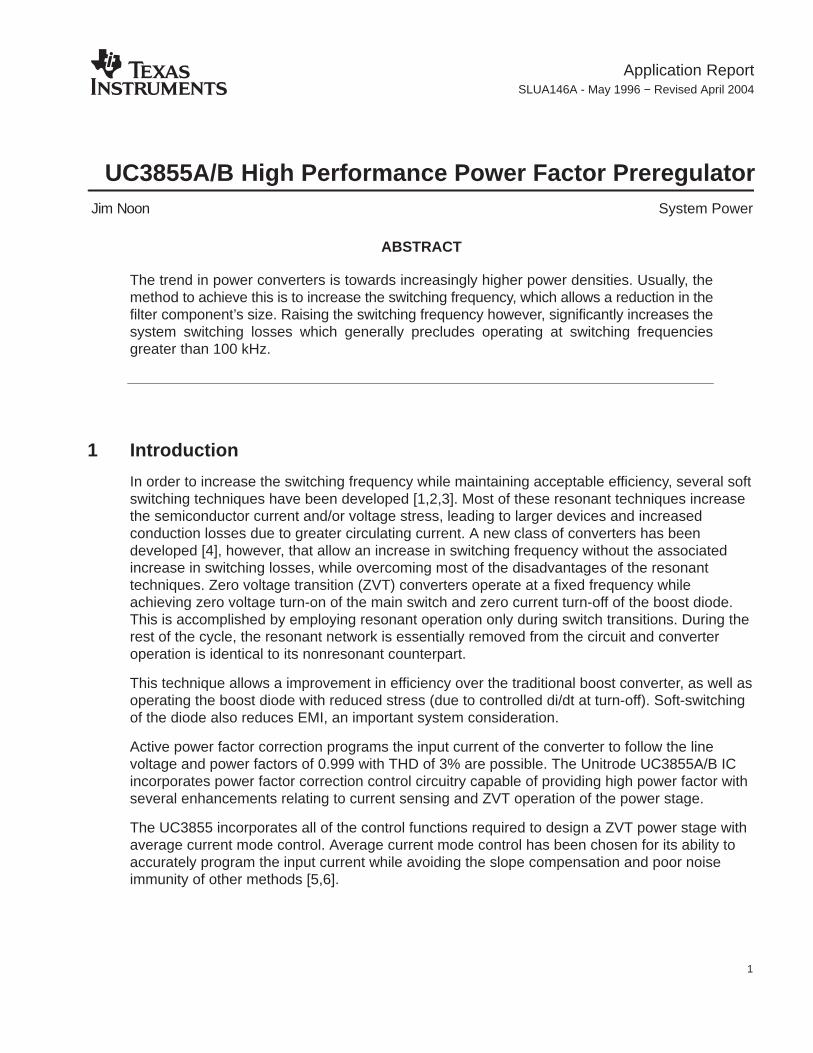
The ZVT boost converter operates the same as a conventional boost converter throughout itsswitching cycle except during the switch transitions. Figure 1 shows the ZVT boost power stage.The ZVT network, consisting of QZVT , D2, Lr, and Cr, provides active snubbing of the boostdiode and main switch. The ZVT circuit operation has been described in [4, 7, 8] and arereviewed here for completeness. Referring to Figure 2, the following timing intervals can bedefined:
UDG-95151
Figure 1. Boost Converter with ZVT Power Stage
VDl
ILr
IQMAIN
VDS
VGSZVT
VGSMAIN
VO
ID
t 0 t1 t2 t3 t4 t5 t6 t 0
VO
lin
Iin
lin
UDG-95152
Figure 2. ZVT Timing Diagram

SLUA146A - May 1996 − Revised April 2004
3 UC3855A/B High Performance Power Factor Preregulator
1.1.2 ZVT Timing
1.1.2.1 t0 − t1
During the time prior to t0, the main switch is off and diode D1 is conducting the full load current.At t0, the auxiliary switch (QZVT) is turned on. With the auxiliary switch on, the current in Lrramps up linearly to IIN. During this time the current in diode D1 is ramping down. When thediode current reaches zero the diode turns off (i.e. soft switching of D1). In the practical circuitsome reverse recovery of the diode occurs since the diode needs time to remove the junctioncharge. The voltage across the ZVT inductor is VO, and therefore the time required to ramp upto Iin is:
t01 IIN
VOLr
1.1.2.2 t1 − t2
At t1, the Lr current has reached IIN and Lr and Cr begins to resonate. This resonant cycledischarges Cr until its voltage equals zero. The dv/dt of the drain voltage is controlled by Cr (Cris the combination of the external CDS and COSS). The current through Lr continues to increasewhile Cr discharges. The time required for the drain voltage to reach zero is 1/4 of the resonantperiod. At the end of this period the body diode of the main switch turns on.
t12
2 LrCr
1.1.2.3 t2 − t3
At the beginning of this interval the switch drain voltage has reached 0 V and the body diode isturned on. The current through the body diode is being driven by the ZVT inductor. The voltageacross the inductor is zero and therefore the current freewheels. At this time, the main switchcan be turned on to achieve zero voltage switching.

SLUA146A - May 1996 − Revised April 2004
4 UC3855A/B High Performance Power Factor Preregulator
1.1.2.4 t3 − t4
At t3, the UC3855 senses that the drain voltage of QMAIN has fallen to zero and turns on themain switch while turning off the ZVT switch. After the ZVT switch turns off, the energy in Lr isdischarged linearly through D2 to the load.
1.1.2.5 t4 − t5
At t4, the current in D2 goes to zero. When this occurs, the circuit is operating like a conventionalboost converter. In a practical circuit however, Lr resonates with COSS of the ZVT switch drivingthe node at the anode of D1 negative (since the opposite end of Lr is clamped to zero). Thiseffect is discussed in the ZVT circuit design section.
1.1.2.6 t5 − t6
This stage is also exactly like a conventional boost converter. The main switch turns off. TheQMAIN drain-to-source node capacitance charges to VO and the main diode begins to supplycurrent to the load. Since the node capacitance initially holds the drain voltage to zero, the turnoff losses are significantly reduced.
It can be seen through the above description that the operation of the converter differs from theconventional boost only during the turn-on switch transitions. The main power stage componentsexperience no more voltage or current stress than normal, and the switch and diode bothexperience soft switching transitions. Having significantly reduced the switching losses, theoperating frequency can be increased without an efficiency penalty. The diode also operateswith much lower losses and therefore operates at a lower temperature, increasing reliability. Thesoft switching transitions also reduce EMI, primarily caused by hard turn-off of the boost diode.

SLUA146A - May 1996 − Revised April 2004
5 UC3855A/B High Performance Power Factor Preregulator
1.1.3 Control Circuit Requirements
In order to maintain zero voltage switching for the main switch, the ZVT switch must be on untilthe voltage on Cr resonates to zero. This can be accomplished by using a fixed delay equal totZVT at low line and maximum load.
tZVT IIN(p) Lr
VO
2 Lr Cr
However, this would give a longer than necessary delay at lighter load or higher line conditions,and therefore would increase the ZVT circuit conduction loss and increase the peak currentstress. The UC3855 allows for a variable tZVT by sensing when the QMAIN drain voltage hasfallen to zero. Once the voltage falls below the ZVS pin threshold voltage (2.5 V), the ZVT gatedrive signal is terminated and the main switch gate drive goes high. The control waveforms areshown in Figure 3. The switching period begins when the oscillator begins to discharge, and theZVT gate drive goes high at the beginning of the discharge period. The ZVT signal stays highuntil the ZVS pin senses the zero voltage condition or until the discharge period is over (theoscillator discharge time is the maximum ZVT pulse width). This allows the ZVT switch to be ononly for as long as necessary.
UDG-95153
Figure 3. ZVT Control Waveforms
SLUA146A - May 1996 − Revised April 2004
6 UC3855A/B High Performance Power Factor Preregulator
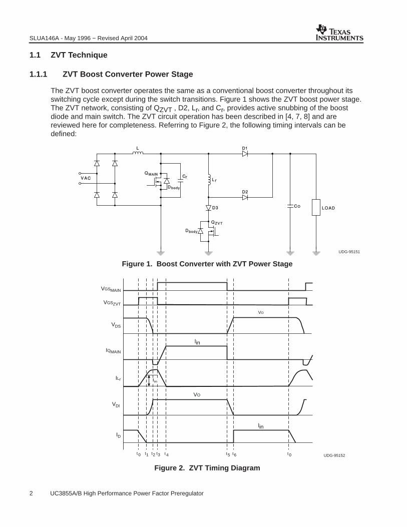
2 Control Circuit Operation and Design
Figure 4 shows the UC3855A/B block diagram (pin numbers correspond to DIL−20 packages). Itshows a controller which incorporates the basic PFC circuitry, including average current modecontrol, and the drive circuitry to facilitate ZVT operation. The device also has current waveformsynthesizer circuitry to simplify current sensing, as well as overvoltage and overcurrentprotection. In the following sections the control device is broken down into functional blocks andindividually reviewed.
UDG-94001-2
Figure 4. UC3855 Controller Block Diagram

SLUA146A - May 1996 − Revised April 2004
7 UC3855A/B High Performance Power Factor Preregulator
2.1 Comparison with UC3854A/B
The PFC section of the UC3855A/B is identical to the UC3854A/B. Several common designparameters are highlighted below to illustrate the similarities.
FUNCTION UC3854A/B UC3855A/B
Enable Dedicated pin Incorporated into OVP
Design range for VRMS 1.5 V to 4.7 V 1.5 V to 4.7 V
VREF for VA 3 V 3 V
Maximum VA output volt-age 6 V 6 V
Offset voltage at IAC 0.5 V 0.7 V
Multiplier gainIAC(VA 1.5)
VRMS2 IMO
IAC(VA 1.5)
VRMS2 IMO
New features incorporated into the UC3855A/B include:
• ZVT control circuitry
• Overvoltage protection
• Current synthesizer
2.2 Oscillator
The oscillator contains an internal current source and sink and therefore only requires anexternal timing capacitor (CT) to set the frequency. The nominal charge current is set to 500 µAand the discharge current is 8 mA. The discharge time is approximately 6% of the total period,which defines the maximum ZVT time. CT is calculated by:
CT 111200 fS
2.3 ZVT Control Circuit
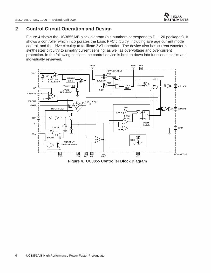
As stated in the ZVT Technique section, the UC3855A/B provides the control logic to ensureZVT operation over all line and load conditions without using a fixed delay. The ZVS pin sensesthe MOSFET drain voltage and is an input to the ZVT drive comparator. The other comparatorinput is internally biased to 2.5 V. When the ZVS input is above 2.5 V (and the PWM clock signalis present) the ZVT drive signal can go high. Pulling the ZVS pin low terminates the ZVT drivesignal and turn on the main switch output (recall that the maximum ZVT output signal is equal tothe oscillator discharge time). The network used to sense the node voltage is shown in Figure 5.R12 pulls up the pin to a maximum of 7.5 V, and C6 provides filtering.
SLUA146A - May 1996 − Revised April 2004
8 UC3855A/B High Performance Power Factor Preregulator
UDG-95154
Figure 5. ZVS Sensing Circuit
The RC time constant should be fast enough to reach 2.5 V at maximum duty cycle. The drainvoltage is limited by the node capacitance which slows down the dv/dt across the mainMOSFET, which reduces the high speed requirement on the ZVS circuit. The maximum ZVS pinvoltage should be limited to VREF, otherwise the ZVS circuitry can become latched and does notoperate properly.
An alternative method for ZVS operation, is to sense the drain voltage through a simple voltagedivider. This voltage still has to be filtered (and clamped) however, so as not to inject noise intothe ZVS pin.
Refer back to Figure 3 for the timing waveforms.
3 Gate Drives
The main drive can source 1.5 APK and the ZVT drive is 0.75 APK. The main switch driveimpedance requirements are reduced due to ZVT operation. At turn-on the drain voltage is atzero volts and therefore the Miller capacitance effect is not an issue, and during turn-off, thedv/dt is limited by the resonant capacitor. Since the ZVT MOSFET is generally at least two diesizes smaller than the main switch, its drive requirements are met with a lower peak currentcapability.
3.1 Multiplier/Divider Circuit
The multiplier section of the UC3855A/B is identical to the UC3854A/B. It incorporates inputvoltage feedforward (through the VRMS input) to eliminate loop gain dependence on the inputvoltage. There are only three parameters (VVRMS, IIAC, and RIMO) that need to be defined toproperly set up the device.

SLUA146A - May 1996 − Revised April 2004
9 UC3855A/B High Performance Power Factor Preregulator
3.1.1 VRMS
The multiplier programs the line current and therefore effects the power drawn from the line. TheVRMS pin is programmed by looking at the system power limits. Referring to the block diagram(Figure 4), the multiplier output equation is:
IIMO IIAC VEA 1.5
V2VRMS
The power limit function is set by the maximum output voltage of the voltage loop error amplifier,VEA (6 V). The power limiting function is easily explained by looking at what happens for a givenvalue of VEA . If the AC line decreases by a factor of two, the feedforward voltage effect(V2VRMS) decreases to one fourth. This increases multiplier output current (and therefore linecurrent) by two. The power drawn from the line has therefore remained constant. Conversely, ifthe load increases and the line stays constant, VEA increases, causing more line current to bedrawn. It can be seen then, that VEA is a voltage proportional to input power.
Normally the multiplier is set to limit maximum power at low line, corresponding to maximumerror amplifier output voltage. The multiplier equation can be solved for the feedforward voltagethat corresponds to maximum error amplifier voltage and maximum multiplier current (internallylimited to 2 times IIAC).
V2VRMS IIAC VEA 1.5
2 IIAC
V2VRMS 1.5
Knowing the VRMS voltage at low line defines the voltage divider from the line to VRMS pin.This feedforward voltage must be relatively free of ripple in order to reduce the amount ofsecond order harmonic that is present at the multiplier input (which in turn would cause 3rd orderharmonics in the input current) [9]. The filtering produces a dc voltage at the VRMS pin. Sincethe input voltage is defined in terms of its RMS value, the dc to RMS factor (0.9) must be takeninto account [9]. For example, if the low line voltage is 85 V, the attenuation required is:
85 VRMS (0.9)
1.5 VDC 51 : 1
At a high line of 270 V, this corresponds to VVRMS = 4.76 V. The common mode range of theVRMS input is 0 V to 5.5 V. The calculated range is therefore within the accepted limits.
A two pole filter is recommended to provide adequate attenuation without degrading thefeedforward transient response. A single pole filter requires a pole at too low of a frequency tostill allow VRMS to respond quickly enough to changes in line voltage.
The filter poles can be calculated once the distortion contribution from VRMS is determined. If thefeedforward circuit’s contribution to the total distortion is limited to 1.5%, the required attenuationof the filter can be calculated. Recall that the percentage of 2nd harmonic in a full wave rectifiedsinewave is approximately 66.7% of the dc value. The percentage of second harmonictranslates to the same percent 3rd harmonic distortion in the input current waveform [9].Therefore, the filter attenuation required is:
1.5%66.7%
0.0025

SLUA146A - May 1996 − Revised April 2004
10 UC3855A/B High Performance Power Factor Preregulator
The individual stages should have an attenuation of or 0.15. For a single stage filter:
AV fCf fC 120 Hz(0.15) 18 Hz
Referring to Figure 6 the components correspond to R9A = R9B = 390 kΩ, R10 = 120 kΩ, andR11 = 18 kΩ with C4 = 0.082 µF and C5 = 0.47 µF.
UDG-95155
Figure 6. V RMS Circuit
3.1.2 IIAC
The value of IIAC is chosen to be 500 µA at high line. This value is somewhat arbitrary, howeverit should be kept below 1 mA to stay within the linear region of the multiplier. This corresponds toa total resistance of approximately 766 kΩ from the line to IAC pin.
3.1.3 RIMO
The multiplier output resistor can be calculated by recognizing that at low line and maximumload current, the multiplier output voltage equals 1 V (in order to stay below the overcurrent trippoint). This also corresponds to the maximum sense voltage of the current transformer. Themultiplier current under this condition is equal to 1 V/RIMO, and can be equated with themultiplier equation which yields:
1 VRIMO
IIAC VEA 1.5
V2VRMS
At low line IIAC equals 156 µA (if low line = 85 V and IIAC was set to 500 µA at 270 V), VEA is atits maximum of 6 V, and VVRMS is 1.5 V. Therefore RIMO equals 3.2 kΩ.

SLUA146A - May 1996 − Revised April 2004
11 UC3855A/B High Performance Power Factor Preregulator
3.2 Current Synthesizer
Current sensing is simplified due to the current synthesis function built into the UC3855A/B.Switch current is the same as inductor current when the switch is on and can be sensed using asingle current transformer. The current synthesizer charges a capacitor (CI) with a currentproportional to the switch current when the switch is on. During the switch off-time, the inductorcurrent waveform is reconstructed by the controller. To get an accurate measure of the inductorcurrent then, all that is required is to reconstruct the down slope of the inductor current, which isgiven by:
it
VOUT VAC
L
Discharging CI with a current proportional to VOUT − VAC allows reconstruction of the inductorcurrent waveform. The capacitor down slope is:
Vit
IDIS
CI
The UC3855A/B develops IDIS by subtracting IIAC/4, from a current proportional to VOUT. Thevoltage at the RVS pin is regulated at 3 V and therefore picking the RVS resistor sets the currentproportional to VOUT.
IDIS 3 VRRVS
IIAC
4
The ratio of the current in RRvs to IIAC/4 should equal the ratio of VOUT to VAC. Therefore if IIAC /4 is 125 µA, the current through RRVS should be set to 130 µA.
RRVS 3 V130 A
23 k, use 22 k
Equating inductor current slope with capacitor voltage slope, and recognizing that maximumslope occurs when VAC equals zero, CI can be solved for:
CI 3 L NRRVS VOUT RS
where N is the current transformer (CT) turns ratio, (NS / NP) and RS is the current senseresistor.
The current synthesizer has approximately 20 mV of offset. This offset can cause distortion atthe zero crossing of the line current. To null out this offset, a resistor can be connected betweenVREF and the IMO pin. The resistor value is calculated based on RIMO and the offset at theoutput of the synthesizer. For a 20-mV offset and RIMO = 3.3 kΩ a resistor from VREF to IMO of1.2 MΩ cancels the offset.

SLUA146A - May 1996 − Revised April 2004
12 UC3855A/B High Performance Power Factor Preregulator
3.3 Current Sensing
3.3.1 Current Transformer
As was seen in the previous section, synthesizing inductor current with the UC3855A/B is quitesimple. Only switch current needs to be sensed directly, and this is most efficiently done with acurrent sense transformer. Resistive sensing at this power level would result in excessive powerdissipation.
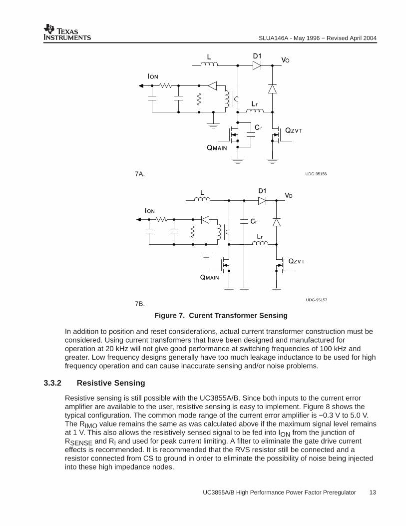
Several issues should be kept in mind when implementing the current transformer. Atfrequencies of a couple hundred kilohertz, core reset needs to be addressed. Contributing to thedifficulty is the very high duty cycles inherent in a power factor correction circuit. In addition, theZVT circuit can complicate the sensing/reset function. When the ZVT circuit turns on, it drawscurrent from the line. In order to minimize line current distortion, this current should bemeasured. Placing the resonant inductor after the current transformer ensures that the ZVTcircuit current is measured. Similarly, when the main switch turns off, current continues to flowinto the resonant capacitor. While it is important to measure this current, if the capacitor isconnected to the drain of the MOSFET, below the current transformer, this current eats into theminimal reset time available at line zero crossings, where duty cycles are approaching 100%.This configuration is shown in Figure 7A. If the current transformer does not have enough timeto reset, it can begin to saturate and lose accuracy, even if complete saturation is avoided,causing distortion at the zero crossings. A better configuration is shown in Figure 7B. In thiscircuit, the capacitor current is measured when it discharges during the ZVT circuit on time.Since this occurs at the beginning of the switching cycle, the current transformer does not loseany of its reset time. Connecting Cr above the current transformer does not adversely affect theMOSFET dv/dt control. Since the device is controlling average current, it does not matterwhether the capacitor current is measured at the beginning or end of the switching cycle.
Figure 7 also shows that filtering is added to the transformer secondary in order to reduce noisefiltering. The bandwidth of this filter should be low enough to reduce switching noise withoutdegrading the switch current waveform.
SLUA146A - May 1996 − Revised April 2004
13 UC3855A/B High Performance Power Factor Preregulator
7A.
7B.
UDG-95156
UDG-95157
Figure 7. Curent Transformer Sensing
In addition to position and reset considerations, actual current transformer construction must beconsidered. Using current transformers that have been designed and manufactured foroperation at 20 kHz will not give good performance at switching frequencies of 100 kHz andgreater. Low frequency designs generally have too much leakage inductance to be used for highfrequency operation and can cause inaccurate sensing and/or noise problems.
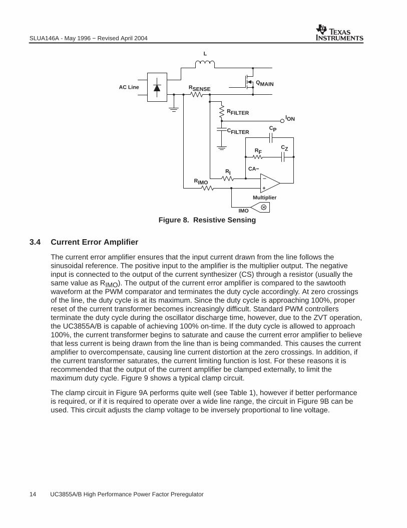
3.3.2 Resistive Sensing
Resistive sensing is still possible with the UC3855A/B. Since both inputs to the current erroramplifier are available to the user, resistive sensing is easy to implement. Figure 8 shows thetypical configuration. The common mode range of the current error amplifier is −0.3 V to 5.0 V.The RIMO value remains the same as was calculated above if the maximum signal level remainsat 1 V. This also allows the resistively sensed signal to be fed into ION from the junction ofRSENSE and RI and used for peak current limiting. A filter to eliminate the gate drive currenteffects is recommended. It is recommended that the RVS resistor still be connected and aresistor connected from CS to ground in order to eliminate the possibility of noise being injectedinto these high impedance nodes.
SLUA146A - May 1996 − Revised April 2004
14 UC3855A/B High Performance Power Factor Preregulator
AC Line RSENSE
RFCZ
CP
CA−RIRIMO
+
Multiplier
IMO
QMAIN
L
RFILTER
CFILTER
ION
Figure 8. Resistive Sensing
3.4 Current Error Amplifier
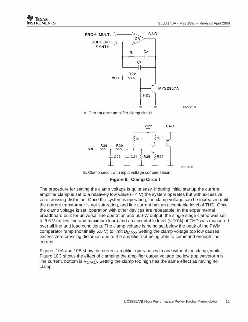
The current error amplifier ensures that the input current drawn from the line follows thesinusoidal reference. The positive input to the amplifier is the multiplier output. The negativeinput is connected to the output of the current synthesizer (CS) through a resistor (usually thesame value as RIMO). The output of the current error amplifier is compared to the sawtoothwaveform at the PWM comparator and terminates the duty cycle accordingly. At zero crossingsof the line, the duty cycle is at its maximum. Since the duty cycle is approaching 100%, properreset of the current transformer becomes increasingly difficult. Standard PWM controllersterminate the duty cycle during the oscillator discharge time, however, due to the ZVT operation,the UC3855A/B is capable of achieving 100% on-time. If the duty cycle is allowed to approach100%, the current transformer begins to saturate and cause the current error amplifier to believethat less current is being drawn from the line than is being commanded. This causes the currentamplifier to overcompensate, causing line current distortion at the zero crossings. In addition, ifthe current transformer saturates, the current limiting function is lost. For these reasons it isrecommended that the output of the current amplifier be clamped externally, to limit themaximum duty cycle. Figure 9 shows a typical clamp circuit.
The clamp circuit in Figure 9A performs quite well (see Table 1), however if better performanceis required, or if it is required to operate over a wide line range, the circuit in Figure 9B can beused. This circuit adjusts the clamp voltage to be inversely proportional to line voltage.
SLUA146A - May 1996 − Revised April 2004
15 UC3855A/B High Performance Power Factor Preregulator
A. Current error amplifier clamp circuit.
B. Clamp circuit with input voltage compensation.
UDG-95159
UDG-95160
Figure 9. Clamp Circuit
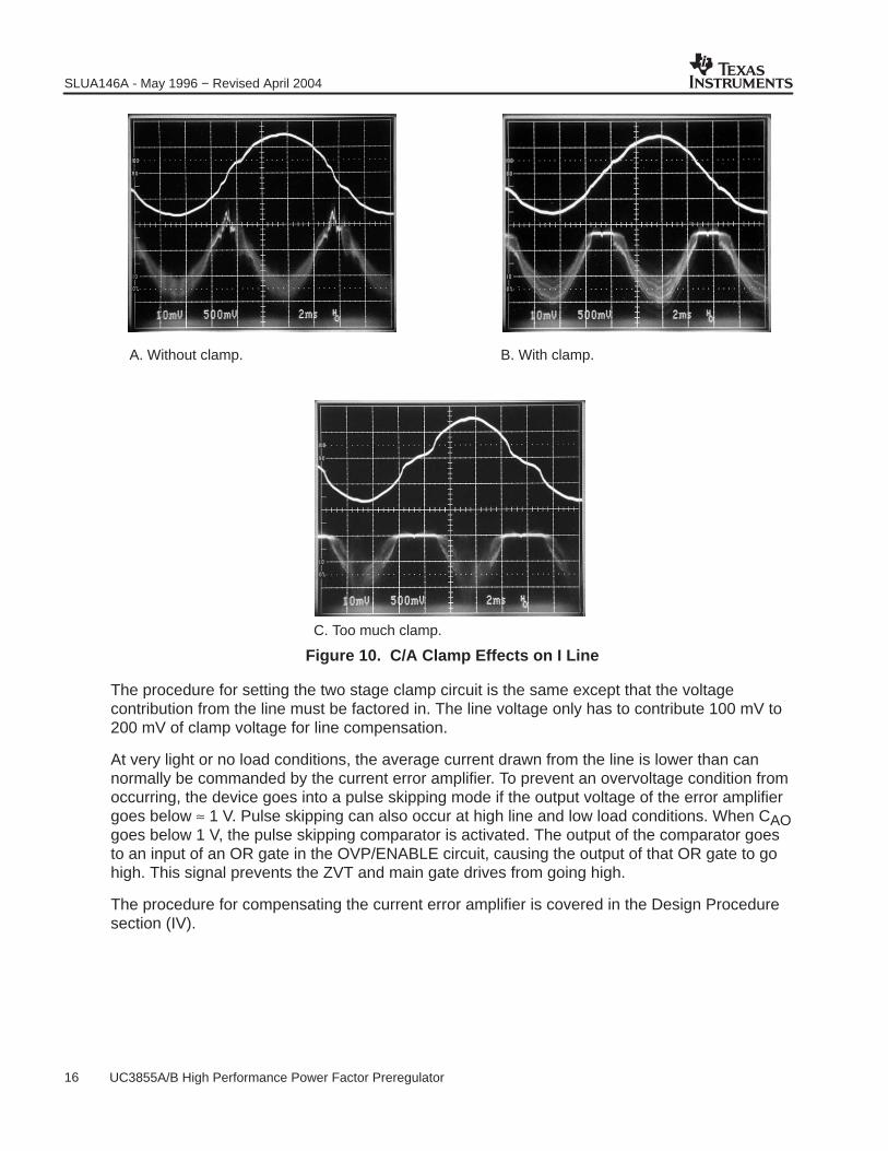
The procedure for setting the clamp voltage is quite easy. If during initial startup the currentamplifier clamp is set to a relatively low value (≈ 4 V) the system operates but with excessivezero crossing distortion. Once the system is operating, the clamp voltage can be increased untilthe current transformer is not saturating, and line current has an acceptable level of THD. Oncethe clamp voltage is set, operation with other devices are repeatable. In the experimentalbreadboard built for universal line operation and 500-W output, the single stage clamp was setto 5.6 V (at low line and maximum load) and an acceptable level (< 10%) of THD was measuredover all line and load conditions. The clamp voltage is being set below the peak of the PWMcomparator ramp (nominally 6.5 V) to limit DMAX. Setting the clamp voltage too low causesexcess zero crossing distortion due to the amplifier not being able to command enough linecurrent.
Figures 10A and 10B show the current amplifier operation with and without the clamp, whileFigure 10C shows the effect of clamping the amplifier output voltage too low (top waveform isline current, bottom is VCAO). Setting the clamp too high has the same effect as having noclamp.
SLUA146A - May 1996 − Revised April 2004
16 UC3855A/B High Performance Power Factor Preregulator
A. Without clamp. B. With clamp.
C. Too much clamp.
Figure 10. C/A Clamp Effects on I Line
The procedure for setting the two stage clamp circuit is the same except that the voltagecontribution from the line must be factored in. The line voltage only has to contribute 100 mV to200 mV of clamp voltage for line compensation.
At very light or no load conditions, the average current drawn from the line is lower than cannormally be commanded by the current error amplifier. To prevent an overvoltage condition fromoccurring, the device goes into a pulse skipping mode if the output voltage of the error amplifiergoes below ≈ 1 V. Pulse skipping can also occur at high line and low load conditions. When CAOgoes below 1 V, the pulse skipping comparator is activated. The output of the comparator goesto an input of an OR gate in the OVP/ENABLE circuit, causing the output of that OR gate to gohigh. This signal prevents the ZVT and main gate drives from going high.
The procedure for compensating the current error amplifier is covered in the Design Proceduresection (IV).

SLUA146A - May 1996 − Revised April 2004
17 UC3855A/B High Performance Power Factor Preregulator
3.5 Voltage Error Amplifier
The output voltage is sensed by the VSENSE input to the voltage error amplifier and comparedto an internally generated reference of 3 V. The output of the amplifier, VEA, (at a given inputvoltage) varies proportionally with output power. The output voltage range for the voltage erroramplifier is approximately 0.1 V to 6 V. The output of the amplifier is one of the multiplier inputs,and an input voltage below 1.5 V inhibits the multiplier output. The design procedure forcompensating the voltage loop is outlined in the Design Procedure section.
3.6 Protection Circuitry
3.6.1 OVP/ENABLE
The UC3855A/B combines the enable and OVP function into one pin. It requires a minimum of1.8 V to enable the device, and below this voltage, the reference is held low and the oscillator isdisabled. A voltage above 7.5 V interrupts the gate drive. The resistor divider should be sized for7.5 V when an over voltage condition is reached, this allows startup at a reasonable line voltage.For example, if an overvoltage condition is defined as an output voltage exceeding 450 V, thenthe voltage divider from VOUT to the OVP pin is 60:1. This divider allows startup at a line voltageof 76 VRMS (108 VPK).
3.6.2 Current Limit
The UC3855A/B has pulse by pulse current limiting. The multiplier power limit determines themaximum average power drawn from the line. However, during transients or overloadconditions, a peak current limiting function is necessary. This function is implemented by sensingthe switch current and feeding this value into ION, to a current limiting comparator thatterminates the gate drive signal if the switch current signal exceeds 1.5 V (nominal).
3.7 Soft Start
In order to ensure a smooth, controlled startup, the UC3855A/B provides a soft-start (SS)function. The SS pin sources 15 µA into an external capacitor. This capacitor limits the supplyvoltage to the voltage loop error amplifier, which effectively limits the output voltage of theamplifier and therefore the maximum commanded output voltage. This allows the output voltageto ramp up in a controlled fashion.
3.7.1 Undervoltage Lockout
The UC3855A has a 15.5 V (nominal) turn-on threshold with 6 V of hysteresis while theUC3855B turns on at 10.5 V with 0.5 V of hysteresis.

SLUA146A - May 1996 − Revised April 2004
18 UC3855A/B High Performance Power Factor Preregulator
4 Typical Application
A typical application is designed in order to illustrate the design procedure and highlight thedesign parameters that need to be defined. The design specifications are:
• VIN = 85 − 270 VAC
• VO = 410 VDC
• PO(max) = 500 W
• FS = 250 kHz
• Eff > 95%
• Pf > 0.993
• THD < 12%
The above specifications represent a common universal input voltage, medium powerapplication. The switching frequency of 250 kHz is now possible due to the soft switching, zerovoltage transitions. The Pf and THD numbers correspond to achievable line correction with theUC3855.
4.1 Design Procedure
This design procedure is a summary of what was presented in [8]. However, several values havebeen changed in order to consolidate component values and/or specify more readily availableparts.
4.2 Power Stage Design
4.2.1 Inductor Design
The power stage inductor design in a ZVT converter is identical to the conventional boostconverter. The inductance required is determined by the amount of switching ripple desired, andallowing more ripple reduces the inductor value. The worst case for peak current occurs at lowline, maximum load. Peak power is equal to twice the average power and VPK is VRMS. Tocalculate input current, assume an efficiency of 95%.
IPK 2 PIN
2 VIN(min)
2 500
0.95
85 8.7 A (60 Hz component)
A good compromise between current ripple and peak current is to allow a 20% ripple to averageratio. This also keeps the peak switch current less than 10 A.
IL 0.2 8.7 A) 1.7 App
Rearranging the conversion ratio for the boost converter to solve for D yields :
D VO VIN
VO
410 2 85410
0.71

SLUA146A - May 1996 − Revised April 2004
19 UC3855A/B High Performance Power Factor Preregulator
We can now calculate the required inductance.
L VIN D TS
I
2 85 V 0.71 4 s
1.7 A 200 H
4.2.2 Output Capacitor Selection
The value of output capacitor effects both hold-up time and output voltage ripple. If hold up time(tH) is the main criteria, the following equation gives a value for CO:
CO 2 PO tH
VO2 V2MIN
In this example a compromise between holdup time and capacitor size was made and acapacitor value of 440 µF was selected. The capacitor bank consists of two 220 µF, 450 VDCcapacitors in parallel.
4.2.3 Power MOSFET & Diode Selection
The main MOSFET selected is an Advanced Power Technology’s APT5020BN (or equivalent).This is a 500-V, 23-A device, with RDS(on) = 0.20 Ω (25°C) and COSS » 500 pF in a TO−247package. A 5.1-Ω resistor is placed in series with the gate to damp any parasitic oscillations atturn-on with a Schottky diode and 2.7-Ω resistor in parallel with the resistor to speed up turn-off.A Schottky is also placed from GTOUT to ground to prevent the pin from being driven belowground, and should be placed as close to the device as possible.
The boost diode selected is the International Rectifier HFA15TB60, a 15-A, 600-V ultrafast diode(or equivalent). Recall that a converter employing ZVT benefits from soft switching of the diode.With ZVT, the boost diode has a negligible impact on switching losses, and therefore a slowerdiode could potentially be used. However, there are still valid reasons for using an ultra fastdiode in this application.
The ZVT inductor is sized according to the recovery time of the diode, and a slower dioderequires a larger inductor. This requires a correspondingly longer QZVT on-time, which increasesconduction loss. A larger inductor also requires a longer time to discharge. To ensure completedischarge of the resonant inductor, the main switch minimum on-time should be approximatelyequal to the ZVT circuit on-time. This yields:
DMIN t01 t12 trr
T
DMIN effects the minimum allowable output voltage for the boost converter to continue operating.The ZVT circuit on-time is a strong function of trr, and therefore choosing an ultra fast diodekeeps the resonant circuit losses to a minimum and cause the least impact on the outputvoltage. The effective system duty cycle is primarily a function of the main switch on-time, sincefor a large portion of the resonant circuit’s on-time, the voltage at the anode of the boost diode isheld up by the resonant capacitor.
These considerations suggest a diode with a recovery time less than 75 ns. Average outputcurrent in this design is less than 1.2 A with a peak current of 9.2 A. The conduction lossassociated with the diode is approximately 2.2 W.
While an ultra fast diode is being used, the diode is operating with significantly reducedswitching losses. This increases the overall system efficiency and reduce the peak stress of thediode.

SLUA146A - May 1996 − Revised April 2004
20 UC3855A/B High Performance Power Factor Preregulator
4.3 ZVT Circuit Design
4.3.1 Resonant Inductor
The ZVT circuit design is straightforward. The circuit is performing an active snubber functionand, as such, the inductor is designed to provide soft turn off of the diode. The ZVT capacitor isselected to provide soft switching of the MOSFET.
The resonant inductor controls the di/dt of the diode by providing an alternate current path forthe boost inductor current. When the ZVT switch turns on, the input current is diverted from theboost diode to the ZVT inductor. The inductor value can be calculated by determining how fastthe diode can be turned off. The diode’s turn-off time is given by its reverse recovery time.Calculating an exact value for Lr is difficult due to the variation in reverse recoverycharacteristics within the actual circuit as well as variations in how reverse recovery is specifiedfrom manufacturer to manufacturer. An example of circuit conditions effecting the reverserecovery is the natural snubbing action of the resonant capacitor, which limits the dv/dt at theanode of the diode. A good initial estimate is to allow the inductor current to ramp up to thediode current within three times the diode’s specified reverse recovery time. One constraint onthe maximum inductance value is its affect on the minimum duty cycle. As was shown in thediode selection section, the L−C time constant effects DMIN and therefore VO(min). Making Lr toolarge also increases the conduction time of the ZVT MOSFET, increasing the resonant circuitconduction losses. As the value of Lr is reduced, the diode experiences more reverse recoverycurrent, and the peak current through the inductor and ZVT MOSFET increases. As the peakcurrent is increased, the amount of energy stored in the inductor also increases (E = 1/2 x L xI2). This energy should be kept to a minimum in order to reduce the amount of parasitic ringingin this node at turn-off.
The reverse recovery of the diode is partially a function of its turn-off di/dt. If a controlled di/dt isassumed, the reverse recovery time of this diode can be estimated to be approximately 60 ns. Ifthe inductor limits the rise time to 180 ns (3 x trr), the inductance can be calculated.
didt
IINp
3 trr 53 As
IINp Ipk 12I
Lr VO
didt 410 V
53 As 7.7 H
The inductor design is limited by core loss and resultant temperature rise, not saturating fluxdensity. This is due to the high ac current component and the relatively high operatingfrequency. A good design procedure is outlined in [10] and is beyond the scope of this review.Several points are mentioned however. The core material should be a good high frequency, lowloss material such as gapped ferrite or molypermalloy powder (MPP). Powder iron coresgenerally are not acceptable in this application. The less expensive Magnetics Kool Mu material,although exhibiting higher losses than the MPP material, can also be used. The higher lossmaterial actually tends to damp the resonant ringing at the turn off of the ZVT switch. Theinductor winding construction is also optimized by keeping interwinding capacitance to aminimum. This reduces the node capacitance at turn off and reduces the amount of dampingrequired.

SLUA146A - May 1996 − Revised April 2004
21 UC3855A/B High Performance Power Factor Preregulator
The inductor current can by found by analyzing the resonant circuit formed by Lr and Cr andrecognizing that the resonant cycle begins when the current reaches Iin.
ILr IIN
VO
Zn sint
where
Zn Lr
Cr , 1
Lr Cr
The peak current then is equal to IIN plus the output voltage divided by the resonant circuit’scharacteristic impedance. Decreasing Lr or increasing Cr increases the peak current. Theinductor was designed using a Magnetics, Inc. MPP core 55209 with 33 turns for an inductanceof 8 µH. The inductor should be constructed with Litz wire or several strands of small magnetwire to minimize high frequency effects.
4.3.2 Resonant Capacitor
The resonant capacitor is sized to ensure a controlled dv/dt of the main switch. The effectiveresonant capacitor is the sum of the MOSFET capacitance and the external node capacitance.The APT5020BN has approximately 500 pF of output capacitance, and an external capacitanceof 500 pF was added across the device. This capacitor limits the dv/dt at turn-off andconsequently reduces the Miller effect. In addition, it reduces turn-off losses since the switchcurrent is diverted to the capacitor. The capacitor must be a good high frequency capacitor, andlow ESR and ESL are required. It must also be capable of handling the relatively large chargingcurrent at turn-off. Two good choices are polypropolene film or a ceramic material.
This combination of L and C yields a resonant quarter cycle of:
2Lr Cr
140 ns
The resonant circuit’s impact on the output voltage can now be calculated. Recall that to ensuredischarge of the resonant inductor at high line:
DMIN t01 t12 trr
T
and for a boost converter:
VO(min) VIN(pk)
1 DMIN
Substituting (1) into (2) and solving for VO produces:
VO(min) Lr IIN(p) VIN(p) T
T trr
2 Lr Cr
Equation (3) can be solved using the previously established values and yields a minimum outputvoltage of 405 V. This suggests a design value of 410 V for VO.
SLUA146A - May 1996 − Revised April 2004
22 UC3855A/B High Performance Power Factor Preregulator
4.3.3 ZVT Switch and Rectifier Selection
The ZVT switch also experiences minimal turn-on loss due to the discharge of its drain-to-sourcecapacitance. However, it does not experience high current and voltage overlap since the turn-oncurrent is limited by the resonant inductor. The switch does experience turn-off and conductionlosses however. Although the peak switch current is actually higher than the main switch current,the duty cycle is small, keeping conduction losses low. The ZVT switch is one or two die sizessmaller than the main switch due to the low average drain current. The ZVT switch on-time is :
tZVT IIN(p) Lr
VO
2 LrCr
The peak ZVT switch current is equal to the peak ZVT inductor current. A conservativeapproximation of the switch RMS current is made by assuming a square wave signal. The RMSof the current is approximated by:
IRMS ILR(pk) tZVT
T
This corresponds to a peak of approximately 14 A at maximum load and maximum ZVT on-time,however, the RMS is only 3.9 A. An appropriate device in this application is the MotorolaMTP8N50E, a 500-V, 8-A device with an RDS(ON) of 0.8 Ω. As with the main MOSFET, a 5.1-Ωresistor is placed in series with the gate to damp any parasitic oscillations at turn on and aSchottky diode and resistor is placed in parallel with the resistor to speed up turn-off. A Schottkyis also placed from ZVTOUT to ground to prevent the pin from being driven below ground. Thisdiode should be placed as close to the device as possible.
The rectifiers needed for the ZVT circuit also experience relatively low RMS current. Diode D2returns the energy stored in the resonant inductor during tZVT to the load. D2 should be anultra-fast recovery diode and is usually chosen to be of similar speed as D1. The diode selectedfor D2 is a Motorola MURH860; a 600-V device with a trr ≈ 35 ns.
Diode D3 blocks current from flowing up through the QZVT body diode when the inductor resets,it sees the same peak and RMS current as QZVT. D3 should be a fast recovery diode todecouple the drain to source capacitance of QZVT from the resonant inductor. Energy stored inthe D3 anode node capacitance resonates with the ZVT inductor when the ZVT switch turns off.Minimizing this effect reduces the amount of snubbing required at this node. The diode chosenhere was the MUR460. This is a 600-V, 4-A device with trr ≈ 75 ns.
To summarize, both diodes in the ZVT circuit experience low RMS current. The main selectioncriteria in addition to the blocking voltage (in both cases equal to VO) is reverse recovery time.Choosing devices with fast recovery times reduces parasitic oscillations, losses, and EMI.

SLUA146A - May 1996 − Revised April 2004
23 UC3855A/B High Performance Power Factor Preregulator
4.3.4 ZVT Snubber Circuit
The ZVT circuit requires some method for damping the parasitic oscillations that occur after theZVT inductor current goes to zero. Figure 10A shows the ZVT inductor current and diode D2anode voltage without adequate damping. The figure shows that as the inductor current beginsto discharge (when QZVT turns off) to the output, the anode voltage is at VOUT (since D2 isconducting). As the inductor current passes through zero, the voltage rings negative since theopposite end of the inductor is clamped to 0 V through the main switch body diode. The anodevoltage can easily ring negatively to twice the output voltage. This increases the reverse voltagestress on the diode to three times the output voltage! Keeping the energy in the nodecapacitance to a minimum and using fast recovery diodes reduces the ringing and improve thecircuit performance.
Several methods of damping this oscillation have been proposed [4,7]. In this circuit twomethods, the saturable reactor and resistive damping were investigated. A 51-Ω, 10-Wnoninductive resistor was connected through a diode from ground to the anode of D2. Thesaturable reactor was placed in series with the resonant inductor and implemented with 8 turnson a Toshiba saturable core SA 14 x 8 x 4.5. The resistive damping method prevents the nodefrom oscillating. However, it does not prevent current from flowing in D2 while D1 is conducting(due to the dv/dt across Lr when QMAIN turns off). If current flows through D2 during this time itexperiences reverse recovery current when QZVT turns on. The saturable reactor prevents thiscurrent flow due to its high impedance. LS also decouples Lr from the node capacitance, whichprevents the node from oscillating.
The saturable reactor works well without the resistive damping and was the method chosen inthis design. With the saturable reactor damping the circuit properly, the resistive damping can beeliminated. However, since LS is designed to saturate each switching cycle, the core loss islargely material dependent and can cause significant temperature rise of the core. In this circuit,heatsinking of the core was required. An alternative design was also tried using the larger MS 18x 12 x 4.5 which ran cooler although it also required heatsinking. Optimization of this circuit cansignificantly reduce the losses in the ZVT circuit. In this design, damping network losses wereapproximately 2 W. Figure 10B shows the same circuit condition with the node damped with LS.
A. Waveforms without damping. B. Waveforms with proper damping.
Figure 11. ZVT Ringing Waveforms

SLUA146A - May 1996 − Revised April 2004
24 UC3855A/B High Performance Power Factor Preregulator
4.3.5 ZVS Circuit
The ZVS circuit components are chosen next. In this example, a 1-kΩ resistor is used to pull upthe ZVS pin. The capacitor chosen is 500 pF. This combination requires approximately 200 ns tocharge up to the 2.5-V threshold.
t R C In1 VTHRESHOLD
VREF
4.4 Oscillator Frequency
Calculate CT:
The switching frequency selected is 250 kHz.
CT 111200 250 kHz
357 pF, use 330 pF
4.5 Multiplier/Divider Circuit
Calculate the VRMS resistor divider:
Set VRMS = 1.5 V at low line (85 VRMS)
divider 85 VRMS 0.9
1.5 VDC 51 : 1
The voltage divider can be solved if one of the resistors is defined (since there are two equationsand three unknowns). Letting the lower resistor in the divider = 18 kΩ:
RTOTAL = 18 kΩ x 51 = 918 kΩ
Letting R10 = 120 kΩ, gives:
R9 = 918 kΩ − 120 kΩ − 18 kΩ = 780 kΩ
R9 is split into two resistors (each 390 kΩ) to reduce their voltage stress.
Calculate the capacitor values to place the filter poles at 18 Hz:
C5 12 fP R11
12 18 Hz 18 k
0.49 F, use 0.47
C4 12 fP REQ
12 18 Hz 117 k
75 nF, use 0.082
where REQ = R9||(R10 + R11) = 117 kΩ

SLUA146A - May 1996 − Revised April 2004
25 UC3855A/B High Performance Power Factor Preregulator
In order to consolidate capacitor values C4 could be chosen to be 0.1 µF without degrading thesystem performance.
Calculate the IAC resistor:
Set IIAC = 500 µA at high line.
R 2 270 V500 A
764 K
Use 2, 390 kΩ resistors in series to reduce voltage stress.
4.5.1 Calculate RIMO
At low line IIAC = 156 µA and the output of the multiplier should equal 1 V. With low line andmaximum load, VEA is at its maximum of 6 V, therefore, using the multiplier output equation:
1VRIMO
IIAC VEA 1.5
VVRMS2
RIMO 1.52
156 A (6 1.5) 3.2 k, use 3.3 k
A 1000-pF capacitor is placed in parallel with RIMO for noise filtering. Since the voltage acrossRIMO is the output of the multiplier and is the reference for the current error amplifier, the RCpole frequency should be placed well above the 120-Hz multiplier signal.
4.6 Current Synthesizer
First, chose a turns ratio for the current transformer. The current transformer is designed toproduce 1 V at peak input current. This allows sufficient margin before the current limit trip point(1.4 V) is reached. If IPK = 9.5 A a turns ratio of 50 : 1 would be appropriate. This turns ratiokeeps the sense network losses less than 150 mW and allow the use of a 1/4-watt resistor.Solving for the sense resistor yields:
RS 1 VISW
N
1 V9.550
5.1
Recall from the previous current synthesizer section that RVS = 22 kΩ. The current synthesizercapacitor can now be calculated:
CI 3 L NRVS VOUT RS
3 200 H 50
22 k 410 V 5.1
633 pF, use 680 pF

SLUA146A - May 1996 − Revised April 2004
26 UC3855A/B High Performance Power Factor Preregulator
4.7 Control Loop Design
4.7.1 Small Signal Model
The small signal model of the ZVT PFC boost converter is similar to the standard PFC boostconverter model. The two converters operate exactly the same throughout most of the switchingcycle and only during the switching transitions is there any difference. This allows the design ofthe control loops to proceed following the standard techniques outlined in [9].
4.7.2 Current Loop Design
Excellent references on the current loop design are found in [5,9,11]. The design of the averagecurrent mode control loop begins with choosing a cross-over frequency. In this example theswitching frequency is 250 kHz, so the unity gain cross over frequency could be chosen to be ashigh as 40 kHz (1/6 of the switching frequency). In this circuit however, the cross over is chosento be 10 kHz. Since the main job of the current loop is to track the line current, a 10 kHzbandwidth is quite adequate for this application.
Once the cross over frequency (fC) is known, the next thing to do is calculate the gain of thepower stage. The small signal model of the power stage including the current sense network isgiven below. This model does not include the sampling effect at one half the switching frequency[12] but is a good approximation at the frequencies of interest.
GID(s) VO RSENSE
S L VSE
The UC3855A/B has an oscillator ramp of 5.2 VPP (VSE). The RSENSE term, is the attenuationfrom actual input current to sensed current (i.e. it includes the current transformer turns ratio).Using the previously determined component values and solving for the power stage gain at fCyields a gain of 0.63 at 10 kHz. In order to have a gain of 1 at fC, the error amplifier must have again of 1/0.63 at 10 kHz. The error amplifier is shown in Figure 12A with the frequency responsein Figure 12B. The resistor RI is equal to 3.3 kΩ so the feedback resistor is chosen to be 5.6 kΩ.A zero is placed at the cross over frequency to give a phase margin of 45 degrees. To reduceswitching noise a pole is placed at one-half the switching frequency. The following summarizesthe design procedure.

SLUA146A - May 1996 − Revised April 2004
27 UC3855A/B High Performance Power Factor Preregulator
B. Current error amplifier schematic.A. Current loop error amplifier.UDG-95161 UDG-95162
Figure 12. Current Error Amplifier Schematic
1. Gid(s) 410 V 0.102 10 kHz 200 H 5.2
0.63
2. GEA 1Gid(s)
1.58 AV Rf
Ri
Rf RI
Gid(s) 5.6 k
3. fZ fC 12 Rf CZ
CZ 12 10 kHz 5.6 k
2200 pF
4. fP 1
2 RfCZCPCZCP
1
2 Rf CP
CP 12 5.6 k 125 kHz
220 pF

SLUA146A - May 1996 − Revised April 2004
28 UC3855A/B High Performance Power Factor Preregulator
4.7.3 Voltage Loop Design
The design of the voltage loop follows the procedure given in [5]. The first step is to determinethe amount of ripple on the output capacitor.
VO(pk) PIN XCO
VO
VO(pk) 525
2 120 410 410 4.14 VPK 8.3 VPP
In order to meet the 3% THD specification, the distortion due to output ripple voltage feedingthrough the voltage error amplifier is limited to 0.75%. This allows 1.5% from the multiplier and0.75% from miscellaneous sources. A 1.5% second harmonic on the error amplifier results in0.75% 3rd harmonic distortion at the input. At full load, the peak error amplifier ripple voltageallowed is:
VEA(pk) %RIPPLE VVEA 0.015 (6 1) 0.075 V
The error amplifier gain at 120 Hz is the allowable error amplifier ripple voltage divided by theoutput ripple voltage, or 0.009 (−41 dB). The error amplifier input resistor was chosen to be1.36 MΩ to keep power dissipation low and allow a small value for the compensation capacitor.Two 681-kΩ resistors in series are used to reduce the voltage stress. The voltage error amplifierschematic is shown in Figure 13, with the 120-Hz gain determined by the integrator function ofCF and RI. This network has a single pole role off and the capacitor value is easily found to givethe desired gain at 120 Hz.
B. Voltage amplifier gain plot.A. Voltage loop error amplifier.
UDG-95163 UDG-95164
Figure 13. Voltage Error Amplifier
CF 12 f GVEA RI
CF 12 120 Hz 0.009 1.36 M
0.1 F

SLUA146A - May 1996 − Revised April 2004
29 UC3855A/B High Performance Power Factor Preregulator
The crossover frequency can now be calculated recognizing that a pole (due to the combinationof Cf and Rf) is placed at the cross over frequency to provide adequate phase margin. The poleplacement determines the phase margin since the power stage has a single pole response withthe associated 90 degree phase lag. If the error amplifier pole is placed at the crossoverfrequency, the overall loop gain has a 45 degree phase margin. The power stage gain is givenby:
GPS(s) VO
VVEA
PIN
VVEA VO S CO
The voltage loop gain (TV) is the product of the power stage gain and the error amplifier gain. Tofind the cross over frequency, solve for f and set equal to 1.
TV 1 GPS(s) GVEA(s)
The error amplifier gain is:
GVEA j
2 f Rj Cf
j 1.17f
TV 1 j 92.6
f j 1.17
f 108
f2
The cross over frequency then is approximately 11 Hz, so the resistor, Rf, can be calculated toplace the pole at f.
Rf 1
2 11 Hz 0.1 F 140 k
Finally, the resistor RD (10 kΩ) sets the dc output voltage to 410 V.
4.8 OVP/ENABLE
An output voltage exceeding 450 V is defined as an overvoltage condition. To trip the OVPcomparator at 450 V requires a divider of:
7.5 V450 V
60 : 1
Setting the lower resistor in the divider = 33 kΩ, the top resistor then is 2 MΩ, two 1-MΩ resistorsare used in series to reduce the voltage stress. A 10-nF capacitor is placed in parallel with the33-kΩ resistor for noise filtering.
With this divider the converter starts at 76 VRMS, which allows startup well below low line.

SLUA146A - May 1996 − Revised April 2004
30 UC3855A/B High Performance Power Factor Preregulator
5 Experimental Results
The example converter was constructed to demonstrate circuit performance. The circuitperformed well and was tested over the full line and load ranges.
Figure 14 shows efficiency data for the ZVT vs. a conventional boost converter, which wasderived by simply removing the ZVT components. The conventional circuit needed to be cooledwith a fan in order to stabilize the power semiconductor temperatures. It can be seen from thedata that the ZVT circuit has a significant advantage over the conventional converter at low line.At higher line voltages the advantage is reduced until the two power stages converge at highline. This is understandable and consistent with the other reported data [4,13]. At low line, thehigher input current contributes to higher switching losses in the conventional converter. TheZVT converter however, does not experience increased switching losses (conduction lossesincrease for both converters at low line).
Figure 14. Efficiency Data
Figure 15 shows the ZVT and main switch gate drives as well as the main switch drain to sourcevoltage. The ZVT gate drive goes high prior to the main switch and drives the drain voltage tozero before the main switch turns on. It should also be noted that the drain to source voltagewaveform is very clean with no overshoot or ringing, which reduces EMI and voltage stress onthe device. The ZVT circuit waveforms are shown in Figure 16. Current in Lr is shown in the toptrace. The waveforms are well damped with a peak current of approximately 6 A. The currentsynthesizer waveforms are shown in Figure 17. The top waveform is the reconstructedwaveform at CI and the bottom waveform is inductor current. The waveforms show goodagreement. Any error between the reconstructed and actual waveform are greatest at high lineand is primarily caused by slight offset voltage errors in the synthesizer circuit.

SLUA146A - May 1996 − Revised April 2004
31 UC3855A/B High Performance Power Factor Preregulator
Figure 15. ZVT Waveforms
Figure 16. Power Stage Waveforms
Figure 17. Current Synthesizer Waveforms

SLUA146A - May 1996 − Revised April 2004
32 UC3855A/B High Performance Power Factor Preregulator
Figure 18 shows the input line current at low line and maximum load, the THD and power factorare well within acceptable limits. Table 1 gives THD and power factor (pf) measurements forseveral line and load conditions with the single stage current error amplifier clamp circuit. Table2 shows THD and pf with the two stage clamp circuit shown in Figure 9B.
Figure 18. Line Current
Table 1. THD and P F vs. Line with Single Stage Error Amplifier Clamp Circuit
LINE (VAC) % THD Pf
100 6.3 0.998
120 4.5 0.999
200 8.9 0.996
230 10 0.995
Table 2. THD and P F vs. Line with Two Stage Error Amplifier Clamp Circuit
LINE (VAC) % THD Pf
100 4.95 0.999
120 5.30 0.998
200 5.45 0.998
230 5.83 0.998
Table 3. Power Stage Vendors
L1,L2 Magnetics, Butler, PA (412) 282−8282
Spike Killer Toshiba, Westboro, MA (508) 836−3939
Qmain APT, Bend, OR (503) 382−8028
D1 International Rectifier, El Segundo, CA (310) 322−3331
QZVT, D2, D3, D4 Motorola, Phoenix, AZ (602) 244−3550

SLUA146A - May 1996 − Revised April 2004
33 UC3855A/B High Performance Power Factor Preregulator
UDG-95165
Figure 19. UC3855A/B Typical Application

SLUA146A - May 1996 − Revised April 2004
34 UC3855A/B High Performance Power Factor Preregulator
6 References
1. [K. H. Liu and F. C. Lee, Resonant Switches − a Unified Approach to ImprovedPerformance of Switching Converters, Proceedings of the InternationalTelecommunications Energy Conference, November 1984
2. W. A. Tabisz and F. C. Lee, Zero−Voltage − Switching Multi−Resonant Technique −ANovel Approach to Improve Performance of High Frequency Quasi−Resonant Converters,IEEE Power Electronics Specialists Conference 1988
3. K. H. Liu and F. C. Lee, Zero−Voltage Switching Techniques in DC/DC Converter Circuits,Proceedings of the Power Electronics Specialists Conference, June 1986
4. G. C. Hua, C. S. Leu, Y. M. Jiang, and F. C. Lee, Novel Zero−Voltage −Transition PWMConverters, IEEE Power Electronics Specialist Conference, 1992
5. L. H. Dixon, High Power Factor Preregulators for Off−Line Power Supplies, UnitrodePower Supply Design Seminar Manual SEM600, 1988 (Republished in subsequentManuals)
6. L. H. Dixon, Average Current Mode Control of Switching Power Supplies, Unitrode PowerSupply Design Seminar Manual SEM700, 1990 (Republished in subsequent Manuals)
7. J. Bazinet and J. OConnor, Analysis and Design of a Zero Voltage Transition PowerFactor Correction Circuit, IEEE Applied Power Electronics Conference, February 1994
8. J. P. Noon, A 250kHz, 500W Power Factor Correction Circuit Employing Zero VoltageTransitions, Unitrode Power Supply Design Seminar Manual SEM1000, 1994
9. L. H. Dixon, High Power Factor Switching Preregulator Design Optimization, UnitrodePower Supply Design Seminar Manual SEM800, 1991
10. L. H. Dixon, Design of Flyback Transformers and Filter Inductors, Unitrode Power SupplyDesign Seminar Manual SEM400, 1985 (Republished in subsequent Manuals)
11. C. Zhou and M. M. Jovanovic, Design Trade−Offs in Continuous Current−Mode ControlledBoost Power Factor Correction Circuits, High Frequency Power Conversion Conference,May 1992
12. W. Tang, R. B. Ridley and F. C. Lee, Small Signal Modeling of Average Current−ModeControl, IEEE Applied Power Electronics Conference, February 1992
13. M. M. Jovanovic, C. Zhou, and P. Liao, Evaluation of Active and Passive SnubberTechniques for Applications in Power Factor correction Boost Converters 6th InternationalConference on Power Semiconductors and their applications (Electronica 1992) MunichGermany, 1992

IMPORTANT NOTICE
Texas Instruments Incorporated and its subsidiaries (TI) reserve the right to make corrections, modifications,enhancements, improvements, and other changes to its products and services at any time and to discontinueany product or service without notice. Customers should obtain the latest relevant information before placingorders and should verify that such information is current and complete. All products are sold subject to TI’s termsand conditions of sale supplied at the time of order acknowledgment.
TI warrants performance of its hardware products to the specifications applicable at the time of sale inaccordance with TI’s standard warranty. Testing and other quality control techniques are used to the extent TIdeems necessary to support this warranty. Except where mandated by government requirements, testing of allparameters of each product is not necessarily performed.
TI assumes no liability for applications assistance or customer product design. Customers are responsible fortheir products and applications using TI components. To minimize the risks associated with customer productsand applications, customers should provide adequate design and operating safeguards.
TI does not warrant or represent that any license, either express or implied, is granted under any TI patent right,copyright, mask work right, or other TI intellectual property right relating to any combination, machine, or processin which TI products or services are used. Information published by TI regarding third-party products or servicesdoes not constitute a license from TI to use such products or services or a warranty or endorsement thereof.Use of such information may require a license from a third party under the patents or other intellectual propertyof the third party, or a license from TI under the patents or other intellectual property of TI.
Reproduction of information in TI data books or data sheets is permissible only if reproduction is withoutalteration and is accompanied by all associated warranties, conditions, limitations, and notices. Reproductionof this information with alteration is an unfair and deceptive business practice. TI is not responsible or liable forsuch altered documentation.
Resale of TI products or services with statements different from or beyond the parameters stated by TI for thatproduct or service voids all express and any implied warranties for the associated TI product or service andis an unfair and deceptive business practice. TI is not responsible or liable for any such statements.
Following are URLs where you can obtain information on other Texas Instruments products and applicationsolutions:
Products Applications
Amplifiers amplifier.ti.com Audio www.ti.com/audio
Data Converters dataconverter.ti.com Automotive www.ti.com/automotive
DSP dsp.ti.com Broadband www.ti.com/broadband
Interface interface.ti.com Digital Control www.ti.com/digitalcontrol
Logic logic.ti.com Military www.ti.com/military
Power Mgmt power.ti.com Optical Networking www.ti.com/opticalnetwork
Microcontrollers microcontroller.ti.com Security www.ti.com/security
Telephony www.ti.com/telephony
Video & Imaging www.ti.com/video
Wireless www.ti.com/wireless
Mailing Address: Texas Instruments
Post Office Box 655303 Dallas, Texas 75265
Copyright 2004, Texas Instruments Incorporated