slos351e –february 2004–revised november … · package option addendum 8-sep-2017...
TRANSCRIPT

+
−
Copyright © 2016,Texas Instruments Incorporated
Product
Folder
Sample &Buy
Technical
Documents
Tools &
Software
Support &Community
An IMPORTANT NOTICE at the end of this data sheet addresses availability, warranty, changes, use in safety-critical applications,intellectual property matters and other important disclaimers. PRODUCTION DATA.
TLV271, TLV272, TLV274SLOS351E –FEBRUARY 2004–REVISED NOVEMBER 2016
TLV27x Family of 550-µA/Ch, 3-MHz, Rail-to-Rail OutputOperational Amplifiers
1
1 Features1• Rail-to-Rail Output• Wide Bandwidth: 3 MHz• High Slew Rate: 2.4 V/µs• Supply Voltage Range: 2.7 V to 16 V• Supply Current: 550 µA/Channel• Input Noise Voltage: 39 nV/√Hz• Input Bias Current: 1 pA• Specified Temperature Range:
– Commercial Grade: 0°C to 70°C– Industrial Grade: −40°C to 125°C
• Ultrasmall Packaging:– 5-Pin SOT-23 (TLV271)– 8-Pin MSOP (TLV272)
• Ideal Upgrade for TLC72x Family
2 Applications• E-Bike• Power Banks• Smoke detectors• Solar Inverters• Low-Power Motor Controls• Battery-Powered Instruments• Building Automation
Operational Amplifier
3 DescriptionOperating from 2.7 V to 16 V over the extendedindustrial temperature range from -40°C to +125°C,the TLV27x is a low power, wide bandwidthoperational amplifier (opamp) with rail to rail output.This makes it an ideal alternative to the TLC27xfamily for applications where rail-to-rail output swingsare essential. The TLV27x provides 3-MHz bandwidthfrom only 550 µA.
Like the TLC27x, the TLV27x is fully specified for 5-Vand ±5-V supplies. The maximum recommendedsupply voltage is 16 V, which allows the devices to beoperated from a variety of rechargeable cells (±8 Vsupplies down to ±1.35 V).
The CMOS inputs enable use in high-impedancesensor interfaces, with the lower voltage operationmaking an attractive alternative for the TLC27x inbattery-powered applications.
All members are available in PDIP and SOIC with thesingles in the small SOT-23 package, duals in theMSOP, and quads in the TSSOP package.
The 2.7-V operation makes it compatible with Li-Ionpowered systems and the operating supply voltagerange of many micropower microcontrollers availabletoday including TI’s MSP430.
Device Information(1)
PART NUMBER PACKAGE BODY SIZE (NOM)
TLV271SOIC (8) 4.98 mm × 3.91 mmSOT-23 (5) 2.90 mm × 1.60 mmPDIP (8) 9.81 mm × 6.35 mm
TLV272SOIC (8) 4.98 mm × 3.91 mmPDIP (8) 9.81 mm × 6.35 mmVSSOP (8) 3.00 mm × 3.00 mm
TLV274SOIC (14) 8.65 mm × 3.91 mmPDIP (14) 3.90 mm × 6.35 mmTSSOP (14) 5.00 mm × 4.40 mm
(1) For all available packages, see the orderable addendum atthe end of the data sheet.
2
TLV271, TLV272, TLV274SLOS351E –FEBRUARY 2004–REVISED NOVEMBER 2016 www.ti.com
Product Folder Links: TLV271 TLV272 TLV274
Submit Documentation Feedback Copyright © 2004–2016, Texas Instruments Incorporated
Table of Contents1 Features .................................................................. 12 Applications ........................................................... 13 Description ............................................................. 14 Revision History..................................................... 25 Device Comparison Table ..................................... 36 Pin Configuration and Functions ......................... 47 Specifications......................................................... 6
7.1 Absolute Maximum Ratings ...................................... 67.2 Recommended Operating Conditions....................... 67.3 Thermal Information: TLV271 ................................... 77.4 Thermal Information: TLV272 ................................... 77.5 Thermal Information: TLV274 ................................... 77.6 Electrical Characteristics: DC Characteristics........... 87.7 Electrical Characteristics: Input Characteristics........ 87.8 Electrical Characteristics: Output Characteristics ..... 97.9 Electrical Characteristics: Power Supply ................ 107.10 Electrical Characteristics: Dynamic Performance . 107.11 Electrical Characteristics: Noise/Distortion
Performance............................................................. 107.12 Typical Characteristics .......................................... 11
8 Detailed Description ............................................ 16
8.1 Overview ................................................................. 168.2 Functional Block Diagram ....................................... 168.3 Feature Description................................................. 178.4 Device Functional Modes........................................ 17
9 Application and Implementation ........................ 189.1 Application Information............................................ 189.2 Typical Application ................................................. 189.3 System Examples .................................................. 19
10 Power Supply Recommendations ..................... 2111 Layout................................................................... 21
11.1 Layout Guidelines ................................................. 2111.2 Layout Example .................................................... 22
12 Device and Documentation Support ................. 2312.1 Documentation Support ........................................ 2312.2 Related Links ........................................................ 2312.3 Receiving Notification of Documentation Updates 2312.4 Community Resource............................................ 2312.5 Trademarks ........................................................... 2312.6 Electrostatic Discharge Caution............................ 2312.7 Glossary ................................................................ 24
13 Mechanical, Packaging, and OrderableInformation ........................................................... 24
4 Revision HistoryNOTE: Page numbers for previous revisions may differ from page numbers in the current version.
Changes from Revision D (February 2004) to Revision E Page
• Added Feature Description section, Device Functional Modes, Application and Implementation section, PowerSupply Recommendations section, Layout section, Device and Documentation Support section, and Mechanical,Packaging, and Orderable Information section ..................................................................................................................... 1
• Deleted Continuous total power dissipation parameter from Absolute Maximum Ratings..................................................... 6• Deleted Dissipation Ratings table .......................................................................................................................................... 7• Deleted Macromodel Information ......................................................................................................................................... 21

3
TLV271, TLV272, TLV274www.ti.com SLOS351E –FEBRUARY 2004–REVISED NOVEMBER 2016
Product Folder Links: TLV271 TLV272 TLV274
Submit Documentation FeedbackCopyright © 2004–2016, Texas Instruments Incorporated
(1) Typical values measured at 5 V, 25°C.
5 Device Comparison Table
DEVICE (1) VDD (V) VIO (μV) IQ/Ch (μA) IIB (pA) GBW (MHz) SR (V/μs) SHUTDOWN RAIL-TO-RAILSINGLES/DUALS/QUADS
TLV27x 2.7 to 16 500 550 1 3 2.4 — O S/D/Q
TLC27x 3 to 16 1100 675 1 1.7 3.6 — — S/D/Q
TLV237x 2.7 to 16 500 550 1 3 2.4 Yes I/O S/D/Q
TLC227x 2.7 to 16 300 1100 1 2.2 3.6 — O D/Q
TLV246x 2.7 to 6 150 550 1300 6.4 1.6 Yes I/O S/D/Q
TLV247x 2.7 to 6 250 600 2 2.8 1.5 Yes I/O S/D/Q
TLV244x 2.7 to 10 300 725 1 1.8 1.4 — O D/Q
1
2
3
4
8
7
6
5GND
1IN+
1IN-
VDD1OUT
2OUT
2IN-
2IN+
3
2
4
51OUT
GND
IN+ IN-
VDD 1
2
3
4
8
7
6
5
OUT
GND
IN+
IN- VDD
NC NC
NC
4
TLV271, TLV272, TLV274SLOS351E –FEBRUARY 2004–REVISED NOVEMBER 2016 www.ti.com
Product Folder Links: TLV271 TLV272 TLV274
Submit Documentation Feedback Copyright © 2004–2016, Texas Instruments Incorporated
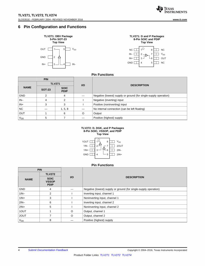
6 Pin Configuration and Functions
TLV271: DBV Package5-Pin SOT-23
Top View
TLV271: D and P Packages8-Pin SOIC and PDIP
Top View
Pin FunctionsPIN
I/O DESCRIPTIONNAME
TLV271
SOT-23 SOICPDIP
GND 2 4 — Negative (lowest) supply or ground (for single-supply operation)IN– 4 2 I Negative (inverting) inputIN+ 3 3 I Positive (noninverting) inputNC — 1, 5, 8 — No internal connection (can be left floating)OUT 1 6 O OutputVDD 5 7 — Positive (highest) supply
TLV272: D, DGK, and P Packages8-Pin SOIC, VSSOP, and PDIP
Top View
Pin FunctionsPIN
I/O DESCRIPTIONNAME
TLV272SOIC
VSSOPPDIP
GND 4 — Negative (lowest) supply or ground (for single-supply operation)1IN– 2 I Inverting input, channel 11IN+ 3 I Noninverting input, channel 12IN– 6 I Inverting input, channel 22IN+ 5 I Noninverting input, channel 21OUT 1 O Output, channel 12OUT 7 O Output, channel 2VDD 8 — Positive (highest) supply

1
2
3
4
5
6
7
14
13
12
11
10
9
8
GND
2IN+
1IN+
2IN-
1IN-
VDD
2OUT
1OUT
3OUT
4OUT
3IN-
4IN-
3IN+
4IN+
5
TLV271, TLV272, TLV274www.ti.com SLOS351E –FEBRUARY 2004–REVISED NOVEMBER 2016
Product Folder Links: TLV271 TLV272 TLV274
Submit Documentation FeedbackCopyright © 2004–2016, Texas Instruments Incorporated
TLV274: D, PW, and N Packages14-Pin SOIC, TSSOP, and PDIP
Top View
Pin FunctionsPIN
I/O DESCRIPTIONNAME
TLV274SOIC
TSSOPPDIP
GND 11 — Negative supply or ground (for single-supply operation)1IN– 2 I Inverting input, channel 11IN+ 3 I Noninverting input, channel 12IN– 6 I Inverting input, channel 22IN+ 5 I Noninverting input, channel 23IN– 9 I Inverting input, channel 33IN+ 10 I Noninverting input, channel 34IN– 13 I Inverting input, channel 44IN+ 12 I Noninverting input, channel 41OUT 1 O Output, channel 12OUT 7 O Output, channel 23OUT 8 O Output, channel 34OUT 14 O Output, channel 4VDD 4 — Positive supply

6
TLV271, TLV272, TLV274SLOS351E –FEBRUARY 2004–REVISED NOVEMBER 2016 www.ti.com
Product Folder Links: TLV271 TLV272 TLV274
Submit Documentation Feedback Copyright © 2004–2016, Texas Instruments Incorporated
(1) Stresses beyond those listed under Absolute Maximum Ratings may cause permanent damage to the device. These are stress ratingsonly, which do not imply functional operation of the device at these or any other conditions beyond those indicated under RecommendedOperating Conditions. Exposure to absolute-maximum-rated conditions for extended periods may affect device reliability. All voltagevalues, except differential voltages, are with respect to GND.
7 Specifications
7.1 Absolute Maximum Ratingsover operating free-air temperature range (unless otherwise noted) (1)
MIN MAX UNIT
VoltageSupply, VDD 16.5 VDifferential input, VID –VDD VDD VInput, VI −0.2 VDD + 0.2 V
CurrentInput, II –10 10 mAOutput, IO –100 100 mA
TemperatureOperating, TA
C-suffix 0 70 °CI-suffix –40 125 °C
Junction, TJ 150 °CStorage, Tstg –65 150 °C
7.2 Recommended Operating Conditionsover operating free-air temperature range (unless otherwise noted)
MIN NOM MAX UNIT
Supply voltage, VDDSingle-supply 2.7 16
VSplit-supply ±1.35 ±8
Common-mode input voltage, VICR 0 VDD −1.35 V
Operating free-air temperature, TAC-suffix 0 70
°CI-suffix –40 125

7
TLV271, TLV272, TLV274www.ti.com SLOS351E –FEBRUARY 2004–REVISED NOVEMBER 2016
Product Folder Links: TLV271 TLV272 TLV274
Submit Documentation FeedbackCopyright © 2004–2016, Texas Instruments Incorporated
(1) For more information about traditional and new thermal metrics, see the Semiconductor and IC Package Thermal Metrics applicationreport.
7.3 Thermal Information: TLV271
THERMAL METRIC (1)
TLV271
UNITD(SOIC)
DBV(SOT-23)
P(PDIP)
8 PINS 5 PINS 8 PINSRθJA Junction-to-ambient thermal resistance 127.2 221.7 49.2 °C/WRθJC(top) Junction-to-case (top) thermal resistance 71.6 144.7 39.4 °C/WRθJB Junction-to-board thermal resistance 68.2 49.7 26.4 °C/WψJT Junction-to-top characterization parameter 22 26.1 15.4 °C/WψJB Junction-to-board characterization parameter 67.6 49 26.3 °C/WRθJC(bot) Junction-to-case (bottom) thermal resistance n/a n/a n/a °C/W
(1) For more information about traditional and new thermal metrics, see the Semiconductor and IC Package Thermal Metrics applicationreport.
7.4 Thermal Information: TLV272
THERMAL METRIC (1)
TLV272
UNITD(SOIC)
DGK(VSSOP)
P(PDIP)
8 PINS 8 PINS 8 PINSRθJA Junction-to-ambient thermal resistance 127.2 186.6 49.2 °C/WRθJC(top) Junction-to-case (top) thermal resistance 71.6 78.8 39.4 °C/WRθJB Junction-to-board thermal resistance 68.2 107.9 26.4 °C/WψJT Junction-to-top characterization parameter 22 15.5 15.4 °C/WψJB Junction-to-board characterization parameter 67.6 106.3 26.3 °C/WRθJC(bot) Junction-to-case (bottom) thermal resistance n/a n/a n/a °C/W
(1) For more information about traditional and new thermal metrics, see the Semiconductor and IC Package Thermal Metrics applicationreport.
7.5 Thermal Information: TLV274
THERMAL METRIC (1)
TLV274
UNITD(SOIC)
N(PDIP)
PW(TSSOP)
14 PINS 14 PINS 14 PINSRθJA Junction-to-ambient thermal resistance 97 66.3 135 °C/WRθJC(top) Junction-to-case (top) thermal resistance 56 20.5 45 °C/WRθJB Junction-to-board thermal resistance 53 26.8 66 °C/WψJT Junction-to-top characterization parameter 19 2.1 n/a °C/WψJB Junction-to-board characterization parameter 46 26.2 60 °C/WRθJC(bot) Junction-to-case (bottom) thermal resistance n/a n/a n/a °C/W

8
TLV271, TLV272, TLV274SLOS351E –FEBRUARY 2004–REVISED NOVEMBER 2016 www.ti.com
Product Folder Links: TLV271 TLV272 TLV274
Submit Documentation Feedback Copyright © 2004–2016, Texas Instruments Incorporated
(1) Full range is 0°C to 70°C for C-suffix and full range is –40°C to 125°C for I-suffix. If not specified, full range is –40°C to 125°C.
7.6 Electrical Characteristics: DC Characteristicsat specified free-air temperature, VDD = 2.7 V, 5 V, and ±5 V (unless otherwise noted)
PARAMETER TEST CONDITIONS TA(1) MIN TYP MAX UNIT
VIO Input offset voltageVIC = VDD/2, RL = 10 kΩ, VO = VDD/2, RS = 50 Ω
25°C 0.5 5mV
Full range 7αVIO Offset voltage drift 25°C 2 µV/°C
CMRR Common-moderejection ratio
VIC = 0 to VDD − 1.35 V,RS = 50 Ω VDD = 2.7 V
25°C 58 70
dB
Full range 55
VIC = 0 to VDD − 1.35 V,RS = 50 Ω VDD = 5 V
25°C 65 80Full range 62
VIC = –5 V to VDD − 1.35 V,RS = 50 Ω VDD = ±5 V
25°C 69 85Full range 66
AVDLarge-signal differentialvoltage amplification
VO(PP) = VDD/2,RL = 10 kΩ
VDD = 2.7 V25°C 97 106
dB
Full range 76
VDD = 5 V25°C 100 110
Full range 86
VDD = ±5 V25°C 100 115
Full range 90
7.7 Electrical Characteristics: Input Characteristicsat specified free-air temperature, VDD = 2.7 V, 5 V, and ±5 V (unless otherwise noted).
PARAMETER TEST CONDITIONS TA MIN TYP MAX UNIT
IIO Input offset current VDD = 5 V, VIC = VDD/2,VO = VDD/2, RS = 50 Ω
25°C 1 60pA70°C 100
125°C 1000
IIB Input bias current VDD = 5 V, VIC = VDD/2,VO = VDD/2, RS = 50 Ω
25°C 1 60pA70°C 100
125°C 1000ri(d) Differential input resistance 25°C 1000 GΩ
CICCommon-mode inputcapacitance f = 21 kHz 25°C 8 pF

9
TLV271, TLV272, TLV274www.ti.com SLOS351E –FEBRUARY 2004–REVISED NOVEMBER 2016
Product Folder Links: TLV271 TLV272 TLV274
Submit Documentation FeedbackCopyright © 2004–2016, Texas Instruments Incorporated
7.8 Electrical Characteristics: Output Characteristicsat specified free-air temperature, VDD = 2.7 V, 5 V, and ±5 V (unless otherwise noted).
PARAMETER TEST CONDITIONS TA MIN TYP MAX UNIT
VOH High-level output voltage
VIC = VDD/2, IOH = –1 mA
VDD = 2.7 V25°C 2.55 2.58
V
Full range 2.48
VDD = 5 V25°C 4.9 4.93
Full range 4.85
VDD = ±5 V25°C 4.92 4.96
Full range 4.9
VIC = VDD/2, IOH = –5 mA
VDD = 2.7 V25°C 1.9 2.1
Full range 1.5
VDD = 5 V25°C 4.6 4.68
Full range 4.5
VDD = ±5 V25°C 4.7 4.84
Full range 4.65
VOL Low-level output voltage
VIC = VDD/2, IOH = 1 mA
VDD = 2.7 V25°C 0.1 0.15
V
Full range 0.22
VDD = 5 V25°C 0.05 0.1
Full range 0.15
VDD = ±5 V25°C –4.95 –4.92
Full range –4.9
VIC = VDD/2, IOH = 5 mA
VDD = 2.7 V25°C 0.5 0.7
Full range 1.1
VDD = 5 V25°C 0.28 0.4
Full range 0.5
VDD = ±5 V25°C –4.84 –4.7
Full range –4.65
IO Output current
VO = 0.5 V from rail,VDD = 2.7 V
Positive rail 25°C 4
mA
Negative rail 25°C 5
VO = 0.5 V from rail,VDD = 5 V
Positive rail 25°C 7Negative rail 25°C 8
VO = 0.5 V from rail,VDD = 10 V
Positive rail 25°C 13Negative rail 25°C 12

10
TLV271, TLV272, TLV274SLOS351E –FEBRUARY 2004–REVISED NOVEMBER 2016 www.ti.com
Product Folder Links: TLV271 TLV272 TLV274
Submit Documentation Feedback Copyright © 2004–2016, Texas Instruments Incorporated
(1) Full range is 0°C to 70°C for C-suffix and full range is –40°C to 125°C for I-suffix. If not specified, full range is –40°C to 125°C.
7.9 Electrical Characteristics: Power Supplyat specified free-air temperature, VDD = 2.7 V, 5 V, and ±5 V (unless otherwise noted).
PARAMETER TEST CONDITIONS TA(1) MIN TYP MAX UNIT
IDDSupply current(per channel) VO = VDD/2
VDD = 2.7 V 25°C 470 560
µAVDD = 5 V 25°C 550 660
VDD = 10 V25°C 625 800
Full range 1000
PSRRSupply voltage rejectionratio(ΔVDD /ΔVIO)
VDD = 2.7 V to 16 V, VIC = VDD/2, no load25°C 70 80
dBFull range 65
(1) Full range is 0°C to 70°C for C suffix and full range is –40°C to 125°C for I suffix. If not specified, full range is –40°C to 125°C.
7.10 Electrical Characteristics: Dynamic Performanceover operating free-air temperature range (unless otherwise noted).
PARAMETER TEST CONDITIONS TA(1) MIN TYP MAX UNIT
UGBW Unity-gain bandwidth RL = 2 kΩ, CL = 10 pFVDD = 2.7 V 25°C 2.4
MHzVDD = 5 V to 10 V 25°C 3
SR Slew rate at unitygain
VO(PP) = VDD/2,CL = 50 pF,RL = 10 kΩ
VDD = 2.7 V25°C 1.35 2.1
V/µsFull range 1
VDD = 5 V25°C 1.45 2.4
V/µsFull range 1.2
VDD = ±5 V25°C 1.8 2.6
V/µsFull range 1.3
φm Phase margin RL = 2 kΩ CL = 10 pF 25°C 65 °Gain margin RL = 2 kΩ CL = 10 pF 25°C 18 dB
tS Setting time
VDD = 2.7 V,V(STEP)PP = 1 V,AV = –1,CL = 10 pFRL = 2 kΩ
0.1%
25°C
2.9
µsVDD = 5 V, ±5 VV(STEP)PP = 1 V,AV = –1,CL = 47 pFRL = 2 kΩ
0.1% 2
7.11 Electrical Characteristics: Noise/Distortion Performanceover operating free-air temperature range (unless otherwise noted).
PARAMETER TEST CONDITIONS TA MIN TYP MAX UNIT
THD + N Total harmonic distortionplus noise
VDD = 2.7 V,VO(PP) = VDD/2 V,RL = 2 kΩ , f = 10 kHz
AV = 125°C
0.02%AV = 10 0.05%AV = 100 0.18%
VDD = 5 V, ±5 V,VO(PP) = VDD/2 V,RL = 2 kΩ , f = 10 kHz
AV = 125°C
0.02%AV = 10 0.09%AV = 100 0.5%
VnEquivalent input noisevoltage
f = 1 kHz25°C
39nV/√Hz
f = 10 kHz 35
InEquivalent input noisecurrent f = 1 kHz 25°C 0.6 fA /√Hz
10 100 1 k 10 k 100 k 1 M
Frequency (Hz)
0
20
40
60
80
100
120
Com
mon-M
ode R
eje
ction R
atio (
dB
)
V = 2.7 VDD
V = 5 V, 10 VDD
-40 -25 -10 20 35 50 65 80 95 110 125
Temperature ( C)°
0
50
-50
100
150
200
250
300
Inp
ut
Bia
s a
nd
Offse
t C
urr
en
t (p
A)
5
V = 2.7 V, 5 V, and 10 VDD
V = V /2IC DD
11
TLV271, TLV272, TLV274www.ti.com SLOS351E –FEBRUARY 2004–REVISED NOVEMBER 2016
Product Folder Links: TLV271 TLV272 TLV274
Submit Documentation FeedbackCopyright © 2004–2016, Texas Instruments Incorporated
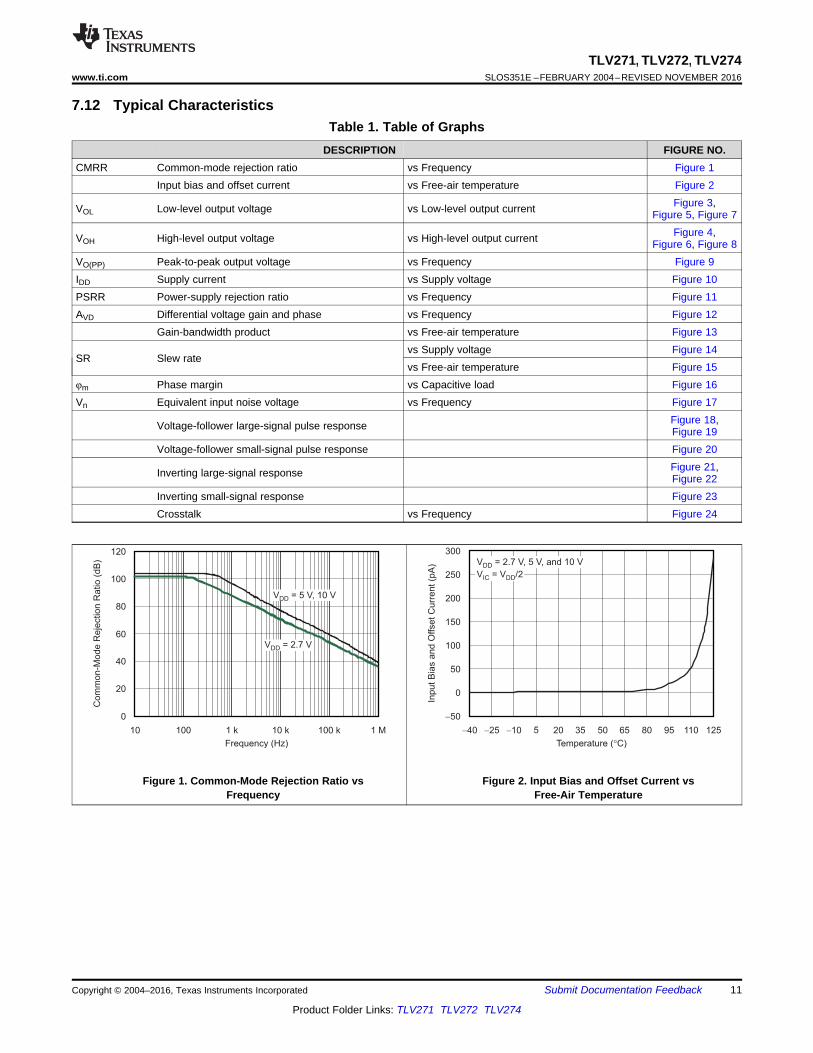
7.12 Typical CharacteristicsTable 1. Table of Graphs
DESCRIPTION FIGURE NO.CMRR Common-mode rejection ratio vs Frequency Figure 1
Input bias and offset current vs Free-air temperature Figure 2
VOL Low-level output voltage vs Low-level output current Figure 3,Figure 5, Figure 7
VOH High-level output voltage vs High-level output current Figure 4,Figure 6, Figure 8
VO(PP) Peak-to-peak output voltage vs Frequency Figure 9IDD Supply current vs Supply voltage Figure 10PSRR Power-supply rejection ratio vs Frequency Figure 11AVD Differential voltage gain and phase vs Frequency Figure 12
Gain-bandwidth product vs Free-air temperature Figure 13
SR Slew ratevs Supply voltage Figure 14vs Free-air temperature Figure 15
φm Phase margin vs Capacitive load Figure 16Vn Equivalent input noise voltage vs Frequency Figure 17
Voltage-follower large-signal pulse response Figure 18,Figure 19
Voltage-follower small-signal pulse response Figure 20
Inverting large-signal response Figure 21,Figure 22
Inverting small-signal response Figure 23Crosstalk vs Frequency Figure 24
Figure 1. Common-Mode Rejection Ratio vsFrequency
Figure 2. Input Bias and Offset Current vsFree-Air Temperature

V = 10 VDD
0 20 60 80 100 120
Low-Level Output Current ( )mA
2
0
6
8
10
Lo
w-L
eve
l O
utp
ut
Vo
lta
ge
(V
)
40
T = 125 CA °
T = 0 CA °
T = 70 CA °
T = 25 CA °
T = 40 CA - °
4
V = 10 VDD
0 20 60 80 100 120
High-Level Output Current ( )mA
2
0
6
8
10
Hig
h-L
eve
l O
utp
ut
Vo
lta
ge
(V
)
40
T = 125 CA °
T = 0 CA °
T = 70 CA °
T = 25 CA °
T = 40 CA - °
4
0 5 10 20 30 35 40 45 50 6055 65 70
Low-Level Output Current ( )mA
0.5
1
0
1.5
2.5
3
3.5
4.5
4
5
Low
-Level O
utp
ut V
oltage (
V)
15 25
V = 5 VDD
T = 125 CA °
T = 0 CA °
T = 70 CA °
T = 25 CA ° T = 40 CA - °2
0 5 10 20 30 35 40 45
High-Level Output Current ( )mA
0.5
1
0
1.5
2.5
3
3.5
4.5
4
5
Hig
h-L
evel O
utp
ut V
oltage (
V)
15 25
2
V = 5 VCC
T = 125 CA °
T = 0 CA °
T = 70 CA °
T = 25 CA °
T = 40 CA - °
0 2 4 8 12 14 16 18 20 22 24
Low-Level Output Current ( )mA
0.4
0.8
0
1.2
1.6
2
2.4
2.8L
ow
-Le
ve
l O
utp
ut
Vo
lta
ge
(V
)
6 10
V = 2.7 VDD
T = 125 CA °
T = 0 CA °
T = 70 CA °
T = 25 CA °
T = 40 CA - °
0 1 2 4 6 7 8 9 10 11 12
High-Level Output Current ( )mA
0.4
0.8
0
1.2
1.6
2
2.4
2.8
Hig
h-L
eve
l O
utp
ut
Vo
lta
ge
(V
)
3 5
V = 2.7 VDD
T = 125 CA ° T = 0 CA °
T = 70 CA °
T = 25 CA °
T = 40 CA - °
12
TLV271, TLV272, TLV274SLOS351E –FEBRUARY 2004–REVISED NOVEMBER 2016 www.ti.com
Product Folder Links: TLV271 TLV272 TLV274
Submit Documentation Feedback Copyright © 2004–2016, Texas Instruments Incorporated
Figure 3. Low-Level Output Voltage vsLow-Level Output Current
Figure 4. High-Level Output Voltage vsHigh-Level Output Current
Figure 5. Low-Level Output Voltage vsLow-Level Output Current
Figure 6. High-Level Output Voltage vsHigh-Level Output Current
Figure 7. Low-Level Output Voltage vsLow-Level Output Current
Figure 8. High-Level Output Voltage vsHigh-Level Output Current

V = 10 VDD
V = 2.7 VDD
V = 5 VDD
-40 -25 -10 20 35 50 65 80 95 110 125
Temperature ( C)°
0.5
0
1
1.5
2
2.5
4
Ga
in B
an
dw
idth
Pro
du
ct
(MH
z)
5
3.5
3
2.5 4.5 8.5 10.5 12.5 14.5
Supply Voltage (V)
0.5
0
1.5
2
3
Sle
w R
ate
(V
/s)
m
6.5
1
2.5
A = 1
R = 10 k
C = 50 pF
T = 25 C
V
L
L
A
W
°
SR +
SR -
10 100 10 k 100 k 1 M
Frequency (Hz)
20
0
80
100
120
Pow
er-
Supply
Reje
ction R
atio (
dB
)
1 k
V = 5 V, 10 VDD
V = 2.7 VDD
40
T = 25 CA °
60
10 100 10 k 100 k 1 M 10 M
Frequency (Hz)
Diffe
ren
tia
l V
olta
ge
Ga
in (
dB
)
1 k
V = 5 VDD
R = 2 k
C = 10 pF
T = 25 C
L
L
A
W
°
20
-40
60
80
100
120
40
-20
0
-45
-180
45
90
135
180
0
-135
-90
Ph
ase
()
°
Phase
Gain
10 100 10 k 100 k 1 M 10 M
Frequency (Hz)
2
0
6
7
8
9
10
11P
ea
k-t
o-P
ea
k O
utp
ut
Vo
lta
ge
(V
)
1 k
V = 5 VDD
V = 2.7 VDD
V = 10 VDD A = 10V -
R = 2 k
C = 10 pF
T = 25 C
THD = 5%
L
L
A
W
°
4
1
3
5
0 1 2 4 6 7 8 9 10 11 15
Supply Voltage (V)
0.4
0.3
0.2
0.1
0.5
0
0.6
0.7
0.8
0.9
1
Su
pp
ly C
urr
en
t (m
A/c
h)
A = 1V
V = V /2IC DD
3 5
T = 125 CA °
141312
T = 70 CA °
T = 25 CA °
T = 0 CA °
T = 40 CA - °
13
TLV271, TLV272, TLV274www.ti.com SLOS351E –FEBRUARY 2004–REVISED NOVEMBER 2016
Product Folder Links: TLV271 TLV272 TLV274
Submit Documentation FeedbackCopyright © 2004–2016, Texas Instruments Incorporated
Figure 9. Peak-to-Peak Output Voltage vsFrequency
Figure 10. Supply Current vsSupply Voltage
Figure 11. Power-Supply Rejection Ratio vsFrequency
Figure 12. Differential Voltage Gain and Phase
Figure 13. Gain Bandwidth Product vsFree-Air Temperature
Figure 14. Slew Rate vsSupply Voltage

Time ( s)m
0
2
4
6
8
Inp
ut
Vo
lta
ge
(V
)
Ou
tpu
t V
olta
ge
(V
)
0
2
4
6
0 2 4 6 8 10 18161412
V = 10 V,DD A = 1
C = 10 pF
V = 6 V
V
L L
I PP , A
R = 2 k
T = 25 C
W,
°
VO
VI
Time ( s)m
0
0.04
0.08
0.12
Inp
ut
Vo
lta
ge
(m
V)
Ou
tpu
t V
olta
ge
(m
V)
0
0.01
0.08
0.12
0 0.2 1.60.4 0.6 0.8 1 1.81.41.2
V = 5 VDD
A = 1
C = 10 pF
V = 100 mV
V
L
L
I PP
A
R = 2 k
T = 25 C
W
°
VO
VI
Time ( s)m
0
1
2
3
4
Inp
ut
Vo
lta
ge
(V
)
Ou
tpu
t V
olta
ge
(V
)
0
1
2
3
0 2 4 6 8 10 18161412
V = 5 VDD
A = 1
C = 10 pF
V = 3 V
V
L
L
I PP
A
R = 2 k
T = 25 C
W
°
VO
VI
10 1 k 10 k100 100 k
Frequency (Hz)
20
0
80
90
100
Eq
uiv
ale
nt
Inp
ut
No
ise
Vo
lta
ge
(n
V/
)H
zÖ
40
60
V = 2.7 V, 5 V, and 10 VDD
T = 25 CA °
70
50
30
10
-40 -25 -10 20 35 50 65 80 95 110 125
Temperature ( C)°
0.5
1
0
1.5
2
2.5
3
3.5S
lew
Ra
te (
V/
s)
m
5
V = 5 VDD
A = 1
R = 10 k
C = 50 pF
V = 3 V
V
L
L
I
W
SR +
SR -
10 100 1000
Capacitive Load (pF)
20
0
80
90
100
Ph
ase
Ma
rgin
()
°
40
60
70
50
30
10
R = 100NULL W
R = 50NULL W
R = 0NULL W
V = 5 VDD
R = 2 k
T = 25 C
A = Open Loop
L
A
V
W
°
14
TLV271, TLV272, TLV274SLOS351E –FEBRUARY 2004–REVISED NOVEMBER 2016 www.ti.com
Product Folder Links: TLV271 TLV272 TLV274
Submit Documentation Feedback Copyright © 2004–2016, Texas Instruments Incorporated
Figure 15. Slew Rate vsFree-Air Temperature
Figure 16. Phase Margin vsCapacitive Load
Figure 17. Equivalent Input Noise Voltage vsFrequency
Figure 18. Voltage-Follower Large-SignalPulse Response
Figure 19. Voltage-Follower Large-SignalPulse Response
Figure 20. Voltage-Follower Small-SignalPulse Response

10 1 k 10 k100 100 k
Frequency (Hz)
-140
-40
-20
0
Cro
ssta
lk (
dB
)
-100Crosstalk
-60
-80
-120
V = 2.7 V, 5 V, and 10 VDD
V = 1 V
A = 1I DD
V
L
A
/2
R = 2 k
T = 25 C
W
°
Time ( s)m
0
0.05
0.1
Input V
oltage (
V)
Outp
ut V
oltage (
V)
0
0.05
0.1VO
VI
V = 5 VDD
A = V = 1
C = 10 pF
V = 100 mV
V I
L
L
I PP
A
-
R = 2 k
T = 25 C
W
°
0 1 1.5 2 2.5 3 4.543.50.5
Time ( s)m
0
1
2
3
4
Inp
ut
Vo
lta
ge
(V
)
Ou
tpu
t V
olta
ge
(V
)
0
1
2
3
0 2 4 6 8 10 161412
V = 5 V,DD A = 1
C = 10 pF
V = 3 V
V
L L
I PP , A
R = 2 k
T = 25 C
W,
°
VO
VI
Time ( s)m
0
2
4
6
8
Inp
ut
Vo
lta
ge
(V
)
Ou
tpu
t V
olta
ge
(V
)
0
2
4
6
0 2 4 6 8 10 161412
VO
VI
V = 10 VDD
A = V = 1
C = 10 pF
V I
L
L
A
-
R = 2 k
T = 25 C
W
°
15
TLV271, TLV272, TLV274www.ti.com SLOS351E –FEBRUARY 2004–REVISED NOVEMBER 2016
Product Folder Links: TLV271 TLV272 TLV274
Submit Documentation FeedbackCopyright © 2004–2016, Texas Instruments Incorporated
Figure 21. Inverting Large-Signal Response Figure 22. Inverting Large-Signal Response
Figure 23. Inverting Small-Signal Response Figure 24. Crosstalk vs Frequency

Copyright © 2016, Texas Instruments Incorporated
Bias
OUT
GND
VDD
IN±
IN+
16
TLV271, TLV272, TLV274SLOS351E –FEBRUARY 2004–REVISED NOVEMBER 2016 www.ti.com
Product Folder Links: TLV271 TLV272 TLV274
Submit Documentation Feedback Copyright © 2004–2016, Texas Instruments Incorporated
8 Detailed Description
8.1 OverviewThe TLV27x operates from a single power supply and consumes only 550 µA of quiescent current. With rail-to-rail output swing capability and 3-MHz bandwidth, the TLV27x is ideal for battery-powered and industrialapplications.
8.2 Functional Block Diagram

+
−RNULL
CLOAD
V /2DD
RG
RF
InputOutput
Copyright © 2016, Texas Instruments Incorporated
V = VOO IO
R
RF
G( (1 +
R
RF
G( (1 +±I RIB+ S ±I RIB F-
+
−+
RS
VI VO
RG
RF
IIB+
IIB-
Copyright © 2016, Texas Instruments Incorporated
17
TLV271, TLV272, TLV274www.ti.com SLOS351E –FEBRUARY 2004–REVISED NOVEMBER 2016
Product Folder Links: TLV271 TLV272 TLV274
Submit Documentation FeedbackCopyright © 2004–2016, Texas Instruments Incorporated
8.3 Feature Description
8.3.1 Rail to Rail OutputThe TLV27x family of opamps features a rail to trail output stage. Rail to rail outputs allow for a wide dynamicrange in low voltage systems. This feature along with low power and wide bandwidth make the TLV27x familysuitable for portable and battery powered systems.
8.3.2 Offset VoltageThe output offset voltage (VOO) is the sum of the input offset voltage (VIO) and both input bias currents (IIB) timesthe corresponding gains. Use the schematic in Figure 25 and Equation 1 to calculate the output offset voltage:
Figure 25. Output Offset Voltage Model
(1)
8.3.3 Driving a Capacitive LoadWhen the amplifier is configured in this manner, capacitive loading directly on the output decreases the devicephase margin, leading to high frequency ringing or oscillations. Therefore, for capacitive loads of greater than 10pF, TI recommends placing a resistor in series (RNULL) with the output of the amplifier, as shown in Figure 26. Aminimum value of 20 Ω should work well for most applications.
Figure 26. Driving a Capacitive Load
8.4 Device Functional ModesThe TLV27x has a single functional mode. It is operational when the power supply applied to the device isbetween 2.7 V (±1.35 V) and 16 V (±8 V). Electrical parameters that can vary with operating conditions areshown in Typical Characteristics.

� �
4
1
C 3 4 2 5
RGain
R
1f 1 R R C C
2S
� �� �� �
1 3 2 52
2 1 3 4 3 4 2 5
1 R R C COutputs
Input s s C 1 R 1 R 1 R 1 R R C C
�
� � � �
4 nF
1 nF2.25 k 1.13 k
2.25 k
+
±
OutputInput
18
TLV271, TLV272, TLV274SLOS351E –FEBRUARY 2004–REVISED NOVEMBER 2016 www.ti.com
Product Folder Links: TLV271 TLV272 TLV274
Submit Documentation Feedback Copyright © 2004–2016, Texas Instruments Incorporated
9 Application and Implementation
NOTEInformation in the following applications sections is not part of the TI componentspecification, and TI does not warrant its accuracy or completeness. TI’s customers areresponsible for determining suitability of components for their purposes. Customers shouldvalidate and test their design implementation to confirm system functionality.
9.1 Application InformationThe TLV27x family offers outstanding DC and AC performance. These devices operate up to a 16-V powersupply and offer ultra-low input bias current and 3-MHz bandwidth. These features make the TLV27x a robustoperational amplifier for battery-powered and industrial applications.
9.2 Typical Application
Figure 27. Second-Order, Low-Pass Filter
9.2.1 Design Requirements• Gain = 1 V/V• Low-pass cutoff frequency = 50 kHz• –40-db/dec filter response• Maintain less than 3-dB gain peaking in the gain versus frequency response
9.2.2 Detailed Design ProcedureThe infinite-gain multiple-feedback circuit for a low-pass network function is shown in Figure 27. Use Equation 2to calculate the voltage transfer function.
(2)
This circuit produces a signal inversion. For this circuit, the gain at DC and the low-pass cutoff frequency arecalculated by Equation 3:
(3)

R
RF
G( (( (1 +
V
VO
I
=1
1 + sR C1 1
1
2 R Cp 1 1
f =-3db
+
−
R1
RG RF
VI
VO
C1
V /2DD
Copyright © 2016, Texas Instruments Incorporated
Frequency (Hz)
Gai
n (d
b)
-60
-40
-20
0
20
100 1k 10k 100k 1M
19
TLV271, TLV272, TLV274www.ti.com SLOS351E –FEBRUARY 2004–REVISED NOVEMBER 2016
Product Folder Links: TLV271 TLV272 TLV274
Submit Documentation FeedbackCopyright © 2004–2016, Texas Instruments Incorporated
Typical Application (continued)Software tools are readily available to simplify filter design. WEBENCH® Filter Designer is a simple, powerful,and easy-to-use active filter design program. The WEBENCH® Filter Designer lets you create optimized filterdesigns using a selection of TI operational amplifiers and passive components from TI's vendor partners.
Available as a web-based tool from the WEBENCH Design Center, WEBENCH Filter Designer allows you todesign, optimize, and simulate complete multistage active filter solutions within minutes.
9.2.3 Application Curve
Figure 28. TLV27x Second-Order, 50-kHz, Low-Pass Filter
9.3 System Examples
9.3.1 General ConfigurationsWhen receiving low-level signals, limiting the bandwidth of the incoming signals into the system is often required.The simplest way to accomplish this limiting is to place an RC filter at the noninverting terminal of the amplifier(see Figure 29 and Equation 4).
Figure 29. Single-Pole Low-Pass Filter
(4)

1
2 RCp
f =-3db
R = R = R
C = C = C
Q = Peaking Factor(Butterworth = 0.707)
1 2
1 2
Q
RF
R =G ( (1Q
2 -
+
−
RG
C1
V /2DD
RF
R1 R2
VI
C2
Copyright © 2016, Texas Instruments Incorporated
20
TLV271, TLV272, TLV274SLOS351E –FEBRUARY 2004–REVISED NOVEMBER 2016 www.ti.com
Product Folder Links: TLV271 TLV272 TLV274
Submit Documentation Feedback Copyright © 2004–2016, Texas Instruments Incorporated
System Examples (continued)If even more attenuation is needed, a multiple pole filter is required. The Sallen-Key filter, shown in Figure 30,can be used for this task. For best results, the amplifier should have a bandwidth that is 8 to 10 times the filterfrequency bandwidth; refer to Equation 5. Failure to use an amplifier with this characteristic can result in phaseshift of the amplifier.
Figure 30. Two-Pole, Low-Pass, Sallen-Key Filter
(5)

21
TLV271, TLV272, TLV274www.ti.com SLOS351E –FEBRUARY 2004–REVISED NOVEMBER 2016
Product Folder Links: TLV271 TLV272 TLV274
Submit Documentation FeedbackCopyright © 2004–2016, Texas Instruments Incorporated
10 Power Supply RecommendationsThe TLV27x is specified for operation from 2.7 V to 16 V (±1.35 V to ±8 V); many specifications apply from–40°C to 125°C. Parameters that can exhibit significant variance with regard to operating voltage or temperatureare presented in the Typical Characteristics.
CAUTIONSupply voltages larger than 16.5 V can permanently damage the device; see theAbsolute Maximum Ratings.
Place 0.1-µF bypass capacitors close to the power-supply pins to reduce errors coupling in from noisy or high-impedance power supplies. For more detailed information on bypass capacitor placement, see LayoutGuidelines.
11 Layout
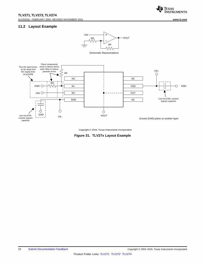
11.1 Layout GuidelinesTo achieve the levels of high performance of the TLV27x, follow proper printed circuit board (PCB) designtechniques. A general set of guidelines is given in the following.• Ground planes—TI highly recommends using a ground plane on the board to provide all components with a
low-inductive ground connection. However, in the areas of the amplifier inputs and output, the ground planecan be removed to minimize the stray capacitance.
• Proper power supply decoupling—Use a 6.8-µF tantalum capacitor in parallel with a 0.1-µF ceramic capacitoron each supply terminal. It may be possible to share the tantalum among several amplifiers depending on theapplication, but a 0.1-µF ceramic capacitor should always be used on the supply terminal of every amplifier.In addition, the 0.1-µF capacitor should be placed as close as possible to the supply terminal. As this distanceincreases, the inductance in the connecting trace makes the capacitor less effective. The designer shouldstrive for distances of less than 0.1 inches between the device power terminals and the ceramic capacitors.
• Sockets—Sockets can be used but are not recommended. The additional lead inductance in the socket pinsoften leads to stability problems. Surface-mount packages soldered directly to the printed-circuit board is thebest implementation.
• Short trace runs/compact part placements—Optimum high performance is achieved when stray seriesinductance has been minimized. To realize this, the circuit layout should be made as compact as possible,thereby minimizing the length of all trace runs. Particular attention should be paid to the inverting input of theamplifier. Its length should be kept as short as possible. This helps to minimize stray capacitance at the inputof the amplifier.
• Surface-mount passive components—Using surface-mount passive components is recommended for highperformance amplifier circuits for several reasons. First, because of the extremely low lead inductance ofsurface-mount components, the problem with stray series inductance is greatly reduced. Second, the smallsize of surface-mount components naturally leads to a more compact layout thereby minimizing both strayinductance and capacitance. If leaded components are used, TI recommends keeping the lead lengths asshort as possible.
NC
IN±
IN+
GND
VDD
OUT
NC
NC
VS+
GND
VS±GND
Ground (GND) plane on another layer VOUT
VIN
GND
Run the input tracesas far away fromthe supply lines
as possible
Use low-ESR, ceramic bypass capacitor
RF
RG
Place components close to device and to each other to reduce
parasitic errors
+VINVOUTRG
RF
(Schematic Representation)
Use low-ESR, ceramic bypass
capacitor
Copyright © 2016, Texas Instruments Incorporated
22
TLV271, TLV272, TLV274SLOS351E –FEBRUARY 2004–REVISED NOVEMBER 2016 www.ti.com
Product Folder Links: TLV271 TLV272 TLV274
Submit Documentation Feedback Copyright © 2004–2016, Texas Instruments Incorporated
11.2 Layout Example
Figure 31. TLV27x Layout Example

23
TLV271, TLV272, TLV274www.ti.com SLOS351E –FEBRUARY 2004–REVISED NOVEMBER 2016
Product Folder Links: TLV271 TLV272 TLV274
Submit Documentation FeedbackCopyright © 2004–2016, Texas Instruments Incorporated
12 Device and Documentation Support
12.1 Documentation Support
12.1.1 Related DocumentationThe following documents are relevant to using the TLV27x, and recommended for reference. All are available fordownload at www.ti.com unless otherwise noted.• Compensate Transimpedance Amplifiers Intuitively (SBOA055)• Operational amplifier gain stability, Part 3: AC gain-error analysis (SLYT383)• Operational amplifier gain stability, Part 2: DC gain-error analysis (SLYT374)• Using the infinite-gain, MFB filter topology in fully differential active filters (SLYT343)• Op Amp Performance Analysis (SBOA054)• Single-Supply Operation of Operational Amplifiers (SBOA059)• Tuning in Amplifiers (SBOA067)• Shelf-Life Evaluation of Lead-Free Component Finishes (SZZA046)
12.2 Related LinksTable 2 lists quick access links. Categories include technical documents, support and community resources,tools and software, and quick access to sample or buy.
Table 2. Related Links
PARTS PRODUCT FOLDER SAMPLE & BUY TECHNICALDOCUMENTS
TOOLS &SOFTWARE
SUPPORT &COMMUNITY
TLV271 Click here Click here Click here Click here Click hereTLV272 Click here Click here Click here Click here Click hereTLV274 Click here Click here Click here Click here Click here
12.3 Receiving Notification of Documentation UpdatesTo receive notification of documentation updates, navigate to the device product folder on ti.com. In the upperright corner, click on Alert me to register and receive a weekly digest of any product information that haschanged. For change details, review the revision history included in any revised document.
12.4 Community ResourceThe following links connect to TI community resources. Linked contents are provided "AS IS" by the respectivecontributors. They do not constitute TI specifications and do not necessarily reflect TI's views; see TI's Terms ofUse.
TI E2E™ Online Community TI's Engineer-to-Engineer (E2E) Community. Created to foster collaborationamong engineers. At e2e.ti.com, you can ask questions, share knowledge, explore ideas and helpsolve problems with fellow engineers.
Design Support TI's Design Support Quickly find helpful E2E forums along with design support tools andcontact information for technical support.
12.5 TrademarksE2E is a trademark of Texas Instruments.WEBENCH is a registered trademark of Texas Instruments.All other trademarks are the property of their respective owners.
12.6 Electrostatic Discharge CautionThese devices have limited built-in ESD protection. The leads should be shorted together or the device placed in conductive foamduring storage or handling to prevent electrostatic damage to the MOS gates.

24
TLV271, TLV272, TLV274SLOS351E –FEBRUARY 2004–REVISED NOVEMBER 2016 www.ti.com
Product Folder Links: TLV271 TLV272 TLV274
Submit Documentation Feedback Copyright © 2004–2016, Texas Instruments Incorporated
12.7 GlossarySLYZ022 — TI Glossary.
This glossary lists and explains terms, acronyms, and definitions.
13 Mechanical, Packaging, and Orderable InformationThe following pages include mechanical, packaging, and orderable information. This information is the mostcurrent data available for the designated devices. This data is subject to change without notice and revision ofthis document. For browser-based versions of this data sheet, refer to the left-hand navigation.

PACKAGE OPTION ADDENDUM
www.ti.com 8-Sep-2017
Addendum-Page 1
PACKAGING INFORMATION
Orderable Device Status(1)
Package Type PackageDrawing
Pins PackageQty
Eco Plan(2)
Lead/Ball Finish(6)
MSL Peak Temp(3)
Op Temp (°C) Device Marking(4/5)
Samples
TLV271CD ACTIVE SOIC D 8 75 Green (RoHS& no Sb/Br)
CU NIPDAU Level-1-260C-UNLIM 0 to 70 T271C
TLV271CDBVR ACTIVE SOT-23 DBV 5 3000 Green (RoHS& no Sb/Br)
CU NIPDAU Level-1-260C-UNLIM 0 to 70 VBHC
TLV271CDBVRG4 ACTIVE SOT-23 DBV 5 3000 Green (RoHS& no Sb/Br)
CU NIPDAU Level-1-260C-UNLIM 0 to 70 VBHC
TLV271CDBVT ACTIVE SOT-23 DBV 5 250 Green (RoHS& no Sb/Br)
CU NIPDAU Level-1-260C-UNLIM 0 to 70 VBHC
TLV271CDBVTG4 ACTIVE SOT-23 DBV 5 250 Green (RoHS& no Sb/Br)
CU NIPDAU Level-1-260C-UNLIM 0 to 70 VBHC
TLV271CDG4 ACTIVE SOIC D 8 75 Green (RoHS& no Sb/Br)
CU NIPDAU Level-1-260C-UNLIM 0 to 70 T271C
TLV271CDR ACTIVE SOIC D 8 2500 Green (RoHS& no Sb/Br)
CU NIPDAU Level-1-260C-UNLIM 0 to 70 T271C
TLV271CDRG4 ACTIVE SOIC D 8 2500 Green (RoHS& no Sb/Br)
CU NIPDAU Level-1-260C-UNLIM 0 to 70 T271C
TLV271ID ACTIVE SOIC D 8 75 Green (RoHS& no Sb/Br)
CU NIPDAU Level-1-260C-UNLIM -40 to 125 T271I
TLV271IDBVR ACTIVE SOT-23 DBV 5 3000 Green (RoHS& no Sb/Br)
CU NIPDAU Level-1-260C-UNLIM -40 to 125 VBHI
TLV271IDBVRG4 ACTIVE SOT-23 DBV 5 3000 Green (RoHS& no Sb/Br)
CU NIPDAU Level-1-260C-UNLIM -40 to 125 VBHI
TLV271IDBVT ACTIVE SOT-23 DBV 5 250 Green (RoHS& no Sb/Br)
CU NIPDAU Level-1-260C-UNLIM -40 to 125 VBHI
TLV271IDBVTG4 ACTIVE SOT-23 DBV 5 250 Green (RoHS& no Sb/Br)
CU NIPDAU Level-1-260C-UNLIM -40 to 125 VBHI
TLV271IDG4 ACTIVE SOIC D 8 75 Green (RoHS& no Sb/Br)
CU NIPDAU Level-1-260C-UNLIM -40 to 125 T271I
TLV271IDR ACTIVE SOIC D 8 2500 Green (RoHS& no Sb/Br)
CU NIPDAU Level-1-260C-UNLIM -40 to 125 T271I
TLV271IP ACTIVE PDIP P 8 50 Pb-Free(RoHS)
CU NIPDAU N / A for Pkg Type -40 to 125 T271I
TLV271IPE4 ACTIVE PDIP P 8 50 Pb-Free(RoHS)
CU NIPDAU N / A for Pkg Type -40 to 125 T271I

PACKAGE OPTION ADDENDUM
www.ti.com 8-Sep-2017
Addendum-Page 2
Orderable Device Status(1)
Package Type PackageDrawing
Pins PackageQty
Eco Plan(2)
Lead/Ball Finish(6)
MSL Peak Temp(3)
Op Temp (°C) Device Marking(4/5)
Samples
TLV272CD ACTIVE SOIC D 8 75 Green (RoHS& no Sb/Br)
CU NIPDAU Level-1-260C-UNLIM 0 to 70 T272C
TLV272CDG4 ACTIVE SOIC D 8 75 Green (RoHS& no Sb/Br)
CU NIPDAU Level-1-260C-UNLIM 0 to 70 T272C
TLV272CDGK ACTIVE VSSOP DGK 8 80 Green (RoHS& no Sb/Br)
CU NIPDAU |CU NIPDAUAG
Level-1-260C-UNLIM 0 to 70 AVF
TLV272CDGKG4 ACTIVE VSSOP DGK 8 80 Green (RoHS& no Sb/Br)
CU NIPDAUAG Level-1-260C-UNLIM 0 to 70 AVF
TLV272CDGKR ACTIVE VSSOP DGK 8 2500 Green (RoHS& no Sb/Br)
CU NIPDAU |CU NIPDAUAG
Level-1-260C-UNLIM 0 to 70 AVF
TLV272CDGKRG4 ACTIVE VSSOP DGK 8 2500 Green (RoHS& no Sb/Br)
CU NIPDAUAG Level-1-260C-UNLIM 0 to 70 AVF
TLV272CDR ACTIVE SOIC D 8 2500 Green (RoHS& no Sb/Br)
CU NIPDAU Level-1-260C-UNLIM 0 to 70 T272C
TLV272CDRG4 ACTIVE SOIC D 8 2500 Green (RoHS& no Sb/Br)
CU NIPDAU Level-1-260C-UNLIM 0 to 70 T272C
TLV272ID ACTIVE SOIC D 8 75 Green (RoHS& no Sb/Br)
CU NIPDAU Level-1-260C-UNLIM -40 to 125 T272I
TLV272IDG4 ACTIVE SOIC D 8 75 Green (RoHS& no Sb/Br)
CU NIPDAU Level-1-260C-UNLIM -40 to 125 T272I
TLV272IDGK ACTIVE VSSOP DGK 8 80 Green (RoHS& no Sb/Br)
CU NIPDAU |CU NIPDAUAG
Level-1-260C-UNLIM -40 to 125 AVG
TLV272IDGKG4 ACTIVE VSSOP DGK 8 80 Green (RoHS& no Sb/Br)
CU NIPDAUAG Level-1-260C-UNLIM -40 to 125 AVG
TLV272IDGKR ACTIVE VSSOP DGK 8 2500 Green (RoHS& no Sb/Br)
CU NIPDAU |CU NIPDAUAG
Level-1-260C-UNLIM -40 to 125 AVG
TLV272IDGKRG4 ACTIVE VSSOP DGK 8 2500 Green (RoHS& no Sb/Br)
CU NIPDAUAG Level-1-260C-UNLIM -40 to 125 AVG
TLV272IDR ACTIVE SOIC D 8 2500 Green (RoHS& no Sb/Br)
CU NIPDAU Level-1-260C-UNLIM -40 to 125 T272I
TLV272IDRG4 ACTIVE SOIC D 8 2500 Green (RoHS& no Sb/Br)
CU NIPDAU Level-1-260C-UNLIM -40 to 125 T272I
TLV272IP ACTIVE PDIP P 8 50 Pb-Free(RoHS)
CU NIPDAU N / A for Pkg Type -40 to 125 T272I
TLV272IPE4 ACTIVE PDIP P 8 50 Pb-Free(RoHS)
CU NIPDAU N / A for Pkg Type -40 to 125 T272I

PACKAGE OPTION ADDENDUM
www.ti.com 8-Sep-2017
Addendum-Page 3
Orderable Device Status(1)
Package Type PackageDrawing
Pins PackageQty
Eco Plan(2)
Lead/Ball Finish(6)
MSL Peak Temp(3)
Op Temp (°C) Device Marking(4/5)
Samples
TLV274CD ACTIVE SOIC D 14 50 Green (RoHS& no Sb/Br)
CU NIPDAU Level-1-260C-UNLIM 0 to 70 TLV274C
TLV274CDG4 ACTIVE SOIC D 14 50 Green (RoHS& no Sb/Br)
CU NIPDAU Level-1-260C-UNLIM 0 to 70 TLV274C
TLV274CDR ACTIVE SOIC D 14 2500 Green (RoHS& no Sb/Br)
CU NIPDAU Level-1-260C-UNLIM 0 to 70 TLV274C
TLV274CDRG4 ACTIVE SOIC D 14 2500 Green (RoHS& no Sb/Br)
CU NIPDAU Level-1-260C-UNLIM 0 to 70 TLV274C
TLV274CPW ACTIVE TSSOP PW 14 90 Green (RoHS& no Sb/Br)
CU NIPDAU Level-1-260C-UNLIM 0 to 70 TLV274C
TLV274CPWG4 ACTIVE TSSOP PW 14 90 Green (RoHS& no Sb/Br)
CU NIPDAU Level-1-260C-UNLIM 0 to 70 TLV274C
TLV274CPWR ACTIVE TSSOP PW 14 2000 Green (RoHS& no Sb/Br)
CU NIPDAU Level-1-260C-UNLIM 0 to 70 TLV274C
TLV274CPWRG4 ACTIVE TSSOP PW 14 2000 Green (RoHS& no Sb/Br)
CU NIPDAU Level-1-260C-UNLIM 0 to 70 TLV274C
TLV274ID ACTIVE SOIC D 14 50 Green (RoHS& no Sb/Br)
CU NIPDAU Level-1-260C-UNLIM -40 to 125 TLV274I
TLV274IDG4 ACTIVE SOIC D 14 50 Green (RoHS& no Sb/Br)
CU NIPDAU Level-1-260C-UNLIM -40 to 125 TLV274I
TLV274IDR ACTIVE SOIC D 14 2500 Green (RoHS& no Sb/Br)
CU NIPDAU Level-1-260C-UNLIM -40 to 125 TLV274I
TLV274IDRG4 ACTIVE SOIC D 14 2500 Green (RoHS& no Sb/Br)
CU NIPDAU Level-1-260C-UNLIM -40 to 125 TLV274I
TLV274IN ACTIVE PDIP N 14 25 Pb-Free(RoHS)
CU NIPDAU N / A for Pkg Type -40 to 125 TLV274I
TLV274INE4 ACTIVE PDIP N 14 25 Pb-Free(RoHS)
CU NIPDAU N / A for Pkg Type -40 to 125 TLV274I
TLV274IPW ACTIVE TSSOP PW 14 90 Green (RoHS& no Sb/Br)
CU NIPDAU Level-1-260C-UNLIM -40 to 125 TLV274I
TLV274IPWG4 ACTIVE TSSOP PW 14 90 Green (RoHS& no Sb/Br)
CU NIPDAU Level-1-260C-UNLIM -40 to 125 TLV274I
TLV274IPWR ACTIVE TSSOP PW 14 2000 Green (RoHS& no Sb/Br)
CU NIPDAU Level-1-260C-UNLIM -40 to 125 TLV274I
TLV274IPWRG4 ACTIVE TSSOP PW 14 2000 Green (RoHS& no Sb/Br)
CU NIPDAU Level-1-260C-UNLIM -40 to 125 TLV274I

PACKAGE OPTION ADDENDUM
www.ti.com 8-Sep-2017
Addendum-Page 4
(1) The marketing status values are defined as follows:ACTIVE: Product device recommended for new designs.LIFEBUY: TI has announced that the device will be discontinued, and a lifetime-buy period is in effect.NRND: Not recommended for new designs. Device is in production to support existing customers, but TI does not recommend using this part in a new design.PREVIEW: Device has been announced but is not in production. Samples may or may not be available.OBSOLETE: TI has discontinued the production of the device.
(2) RoHS: TI defines "RoHS" to mean semiconductor products that are compliant with the current EU RoHS requirements for all 10 RoHS substances, including the requirement that RoHS substancedo not exceed 0.1% by weight in homogeneous materials. Where designed to be soldered at high temperatures, "RoHS" products are suitable for use in specified lead-free processes. TI mayreference these types of products as "Pb-Free".RoHS Exempt: TI defines "RoHS Exempt" to mean products that contain lead but are compliant with EU RoHS pursuant to a specific EU RoHS exemption.Green: TI defines "Green" to mean the content of Chlorine (Cl) and Bromine (Br) based flame retardants meet JS709B low halogen requirements of <=1000ppm threshold. Antimony trioxide basedflame retardants must also meet the <=1000ppm threshold requirement.
(3) MSL, Peak Temp. - The Moisture Sensitivity Level rating according to the JEDEC industry standard classifications, and peak solder temperature.
(4) There may be additional marking, which relates to the logo, the lot trace code information, or the environmental category on the device.
(5) Multiple Device Markings will be inside parentheses. Only one Device Marking contained in parentheses and separated by a "~" will appear on a device. If a line is indented then it is a continuationof the previous line and the two combined represent the entire Device Marking for that device.
(6) Lead/Ball Finish - Orderable Devices may have multiple material finish options. Finish options are separated by a vertical ruled line. Lead/Ball Finish values may wrap to two lines if the finishvalue exceeds the maximum column width.
Important Information and Disclaimer:The information provided on this page represents TI's knowledge and belief as of the date that it is provided. TI bases its knowledge and belief on informationprovided by third parties, and makes no representation or warranty as to the accuracy of such information. Efforts are underway to better integrate information from third parties. TI has taken andcontinues to take reasonable steps to provide representative and accurate information but may not have conducted destructive testing or chemical analysis on incoming materials and chemicals.TI and TI suppliers consider certain information to be proprietary, and thus CAS numbers and other limited information may not be available for release.
In no event shall TI's liability arising out of such information exceed the total purchase price of the TI part(s) at issue in this document sold by TI to Customer on an annual basis.
OTHER QUALIFIED VERSIONS OF TLV271, TLV272, TLV274 :
• Automotive: TLV271-Q1, TLV272-Q1, TLV274-Q1
NOTE: Qualified Version Definitions:
• Automotive - Q100 devices qualified for high-reliability automotive applications targeting zero defects
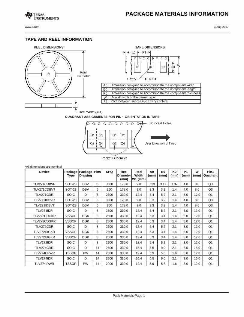
TAPE AND REEL INFORMATION
*All dimensions are nominal
Device PackageType
PackageDrawing
Pins SPQ ReelDiameter
(mm)
ReelWidth
W1 (mm)
A0(mm)
B0(mm)
K0(mm)
P1(mm)
W(mm)
Pin1Quadrant
TLV271CDBVR SOT-23 DBV 5 3000 178.0 9.0 3.23 3.17 1.37 4.0 8.0 Q3
TLV271CDBVT SOT-23 DBV 5 250 178.0 9.0 3.3 3.2 1.4 4.0 8.0 Q3
TLV271CDR SOIC D 8 2500 330.0 12.4 6.4 5.2 2.1 8.0 12.0 Q1
TLV271IDBVR SOT-23 DBV 5 3000 178.0 9.0 3.3 3.2 1.4 4.0 8.0 Q3
TLV271IDBVT SOT-23 DBV 5 250 178.0 9.0 3.3 3.2 1.4 4.0 8.0 Q3
TLV271IDR SOIC D 8 2500 330.0 12.4 6.4 5.2 2.1 8.0 12.0 Q1
TLV272CDGKR VSSOP DGK 8 2500 330.0 12.4 5.3 3.4 1.4 8.0 12.0 Q1
TLV272CDGKR VSSOP DGK 8 2500 330.0 12.4 5.3 3.4 1.4 8.0 12.0 Q1
TLV272CDR SOIC D 8 2500 330.0 12.4 6.4 5.2 2.1 8.0 12.0 Q1
TLV272IDGKR VSSOP DGK 8 2500 330.0 12.4 5.3 3.4 1.4 8.0 12.0 Q1
TLV272IDGKR VSSOP DGK 8 2500 330.0 12.4 5.3 3.4 1.4 8.0 12.0 Q1
TLV272IDR SOIC D 8 2500 330.0 12.4 6.4 5.2 2.1 8.0 12.0 Q1
TLV274CDR SOIC D 14 2500 330.0 16.4 6.5 9.0 2.1 8.0 16.0 Q1
TLV274CPWR TSSOP PW 14 2000 330.0 12.4 6.9 5.6 1.6 8.0 12.0 Q1
TLV274IDR SOIC D 14 2500 330.0 16.4 6.5 9.0 2.1 8.0 16.0 Q1
TLV274IPWR TSSOP PW 14 2000 330.0 12.4 6.9 5.6 1.6 8.0 12.0 Q1
PACKAGE MATERIALS INFORMATION
www.ti.com 3-Aug-2017
Pack Materials-Page 1

*All dimensions are nominal
Device Package Type Package Drawing Pins SPQ Length (mm) Width (mm) Height (mm)
TLV271CDBVR SOT-23 DBV 5 3000 180.0 180.0 18.0
TLV271CDBVT SOT-23 DBV 5 250 180.0 180.0 18.0
TLV271CDR SOIC D 8 2500 340.5 338.1 20.6
TLV271IDBVR SOT-23 DBV 5 3000 180.0 180.0 18.0
TLV271IDBVT SOT-23 DBV 5 250 180.0 180.0 18.0
TLV271IDR SOIC D 8 2500 340.5 338.1 20.6
TLV272CDGKR VSSOP DGK 8 2500 358.0 335.0 35.0
TLV272CDGKR VSSOP DGK 8 2500 364.0 364.0 27.0
TLV272CDR SOIC D 8 2500 340.5 338.1 20.6
TLV272IDGKR VSSOP DGK 8 2500 364.0 364.0 27.0
TLV272IDGKR VSSOP DGK 8 2500 358.0 335.0 35.0
TLV272IDR SOIC D 8 2500 340.5 338.1 20.6
TLV274CDR SOIC D 14 2500 333.2 345.9 28.6
TLV274CPWR TSSOP PW 14 2000 367.0 367.0 35.0
TLV274IDR SOIC D 14 2500 333.2 345.9 28.6
TLV274IPWR TSSOP PW 14 2000 367.0 367.0 35.0
PACKAGE MATERIALS INFORMATION
www.ti.com 3-Aug-2017
Pack Materials-Page 2
www.ti.com
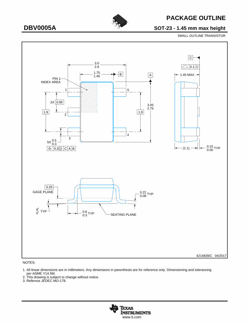
PACKAGE OUTLINE
C
TYP0.220.08
0.25
3.02.6
2X 0.95
1.9
1.45 MAX
TYP0.150.00
5X 0.50.3
TYP0.60.3
TYP80
1.9
A
3.052.75
B1.751.45
(1.1)
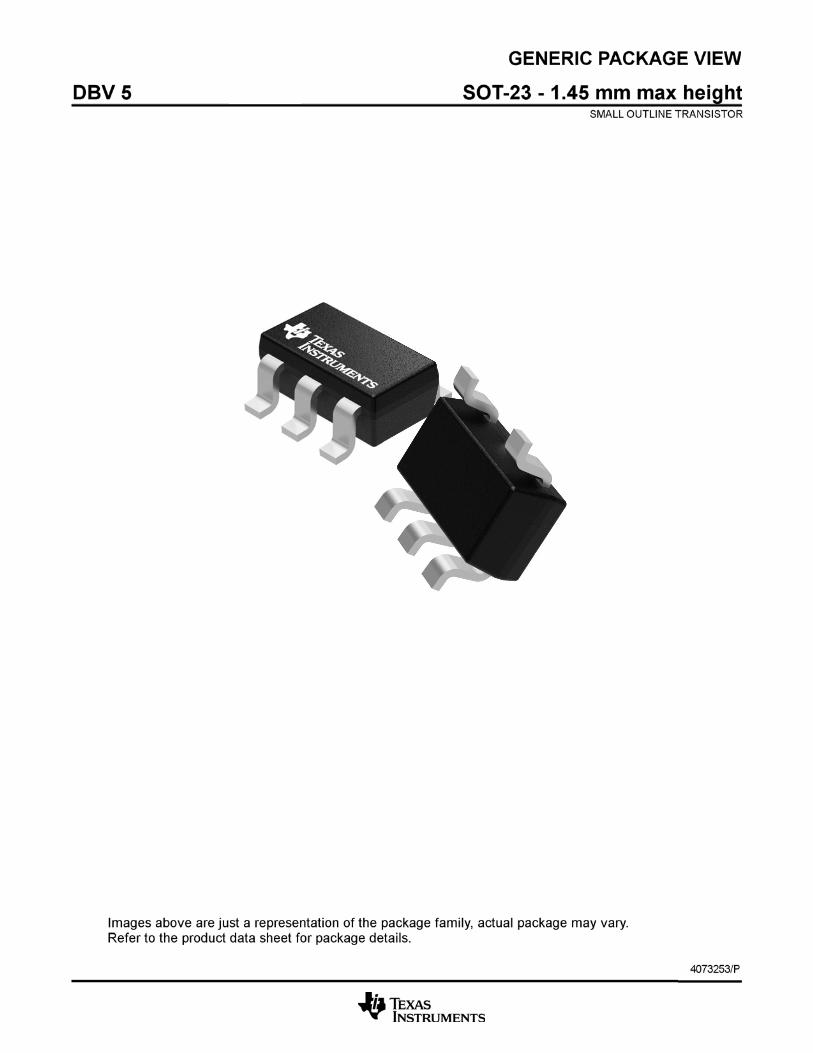
SOT-23 - 1.45 mm max heightDBV0005ASMALL OUTLINE TRANSISTOR
4214839/C 04/2017
NOTES: 1. All linear dimensions are in millimeters. Any dimensions in parenthesis are for reference only. Dimensioning and tolerancing per ASME Y14.5M.2. This drawing is subject to change without notice.3. Refernce JEDEC MO-178.
0.2 C A B
1
34
5
2
INDEX AREAPIN 1
GAGE PLANE
SEATING PLANE
0.1 C
SCALE 4.000

www.ti.com
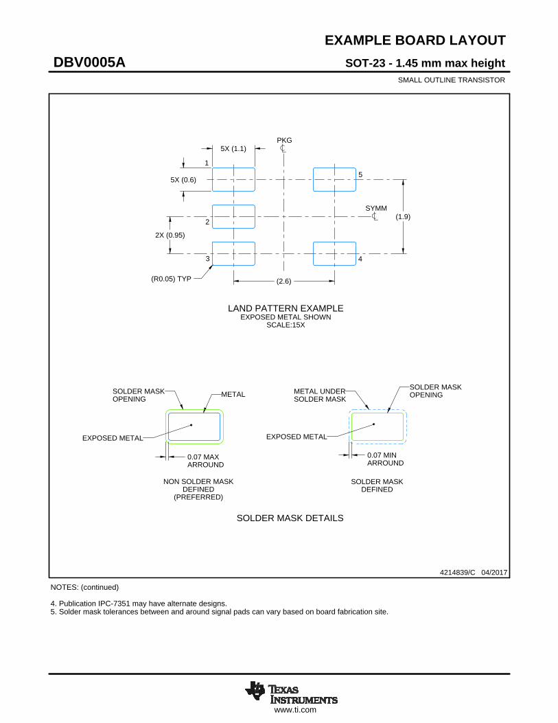
EXAMPLE BOARD LAYOUT
0.07 MAXARROUND
0.07 MINARROUND
5X (1.1)
5X (0.6)
(2.6)
(1.9)
2X (0.95)
(R0.05) TYP
4214839/C 04/2017
SOT-23 - 1.45 mm max heightDBV0005ASMALL OUTLINE TRANSISTOR
NOTES: (continued) 4. Publication IPC-7351 may have alternate designs. 5. Solder mask tolerances between and around signal pads can vary based on board fabrication site.
SYMM
LAND PATTERN EXAMPLEEXPOSED METAL SHOWN
SCALE:15X
PKG
1
3 4
5
2
SOLDER MASKOPENINGMETAL UNDER
SOLDER MASK
SOLDER MASKDEFINED
EXPOSED METAL
METALSOLDER MASKOPENING
NON SOLDER MASKDEFINED
(PREFERRED)
SOLDER MASK DETAILS
EXPOSED METAL

www.ti.com
EXAMPLE STENCIL DESIGN
(2.6)
(1.9)
2X(0.95)
5X (1.1)
5X (0.6)
(R0.05) TYP
SOT-23 - 1.45 mm max heightDBV0005ASMALL OUTLINE TRANSISTOR
4214839/C 04/2017
NOTES: (continued) 6. Laser cutting apertures with trapezoidal walls and rounded corners may offer better paste release. IPC-7525 may have alternate design recommendations. 7. Board assembly site may have different recommendations for stencil design.
SOLDER PASTE EXAMPLEBASED ON 0.125 mm THICK STENCIL
SCALE:15X
SYMM
PKG
1
3 4
5
2

www.ti.com
PACKAGE OUTLINE
C
TYP0.220.08
0.25
3.02.6
2X 0.95
1.9
1.45 MAX
TYP0.150.00
5X 0.50.3
TYP0.60.3
TYP80
1.9
A
3.052.75
B1.751.45
(1.1)
SOT-23 - 1.45 mm max heightDBV0005ASMALL OUTLINE TRANSISTOR
4214839/C 04/2017
NOTES: 1. All linear dimensions are in millimeters. Any dimensions in parenthesis are for reference only. Dimensioning and tolerancing per ASME Y14.5M.2. This drawing is subject to change without notice.3. Refernce JEDEC MO-178.
0.2 C A B
1
34
5
2
INDEX AREAPIN 1
GAGE PLANE
SEATING PLANE
0.1 C
SCALE 4.000
www.ti.com
EXAMPLE BOARD LAYOUT
0.07 MAXARROUND
0.07 MINARROUND
5X (1.1)
5X (0.6)
(2.6)
(1.9)
2X (0.95)
(R0.05) TYP
4214839/C 04/2017
SOT-23 - 1.45 mm max heightDBV0005ASMALL OUTLINE TRANSISTOR
NOTES: (continued) 4. Publication IPC-7351 may have alternate designs. 5. Solder mask tolerances between and around signal pads can vary based on board fabrication site.
SYMM
LAND PATTERN EXAMPLEEXPOSED METAL SHOWN
SCALE:15X
PKG
1
3 4
5
2
SOLDER MASKOPENINGMETAL UNDER
SOLDER MASK
SOLDER MASKDEFINED
EXPOSED METAL
METALSOLDER MASKOPENING
NON SOLDER MASKDEFINED
(PREFERRED)
SOLDER MASK DETAILS
EXPOSED METAL

www.ti.com
EXAMPLE STENCIL DESIGN
(2.6)
(1.9)
2X(0.95)
5X (1.1)
5X (0.6)
(R0.05) TYP
SOT-23 - 1.45 mm max heightDBV0005ASMALL OUTLINE TRANSISTOR
4214839/C 04/2017
NOTES: (continued) 6. Laser cutting apertures with trapezoidal walls and rounded corners may offer better paste release. IPC-7525 may have alternate design recommendations. 7. Board assembly site may have different recommendations for stencil design.
SOLDER PASTE EXAMPLEBASED ON 0.125 mm THICK STENCIL
SCALE:15X
SYMM
PKG
1
3 4
5
2


IMPORTANT NOTICE
Texas Instruments Incorporated (TI) reserves the right to make corrections, enhancements, improvements and other changes to itssemiconductor products and services per JESD46, latest issue, and to discontinue any product or service per JESD48, latest issue. Buyersshould obtain the latest relevant information before placing orders and should verify that such information is current and complete.TI’s published terms of sale for semiconductor products (http://www.ti.com/sc/docs/stdterms.htm) apply to the sale of packaged integratedcircuit products that TI has qualified and released to market. Additional terms may apply to the use or sale of other types of TI products andservices.Reproduction of significant portions of TI information in TI data sheets is permissible only if reproduction is without alteration and isaccompanied by all associated warranties, conditions, limitations, and notices. TI is not responsible or liable for such reproduceddocumentation. Information of third parties may be subject to additional restrictions. Resale of TI products or services with statementsdifferent from or beyond the parameters stated by TI for that product or service voids all express and any implied warranties for theassociated TI product or service and is an unfair and deceptive business practice. TI is not responsible or liable for any such statements.Buyers and others who are developing systems that incorporate TI products (collectively, “Designers”) understand and agree that Designersremain responsible for using their independent analysis, evaluation and judgment in designing their applications and that Designers havefull and exclusive responsibility to assure the safety of Designers' applications and compliance of their applications (and of all TI productsused in or for Designers’ applications) with all applicable regulations, laws and other applicable requirements. Designer represents that, withrespect to their applications, Designer has all the necessary expertise to create and implement safeguards that (1) anticipate dangerousconsequences of failures, (2) monitor failures and their consequences, and (3) lessen the likelihood of failures that might cause harm andtake appropriate actions. Designer agrees that prior to using or distributing any applications that include TI products, Designer willthoroughly test such applications and the functionality of such TI products as used in such applications.TI’s provision of technical, application or other design advice, quality characterization, reliability data or other services or information,including, but not limited to, reference designs and materials relating to evaluation modules, (collectively, “TI Resources”) are intended toassist designers who are developing applications that incorporate TI products; by downloading, accessing or using TI Resources in anyway, Designer (individually or, if Designer is acting on behalf of a company, Designer’s company) agrees to use any particular TI Resourcesolely for this purpose and subject to the terms of this Notice.TI’s provision of TI Resources does not expand or otherwise alter TI’s applicable published warranties or warranty disclaimers for TIproducts, and no additional obligations or liabilities arise from TI providing such TI Resources. TI reserves the right to make corrections,enhancements, improvements and other changes to its TI Resources. TI has not conducted any testing other than that specificallydescribed in the published documentation for a particular TI Resource.Designer is authorized to use, copy and modify any individual TI Resource only in connection with the development of applications thatinclude the TI product(s) identified in such TI Resource. NO OTHER LICENSE, EXPRESS OR IMPLIED, BY ESTOPPEL OR OTHERWISETO ANY OTHER TI INTELLECTUAL PROPERTY RIGHT, AND NO LICENSE TO ANY TECHNOLOGY OR INTELLECTUAL PROPERTYRIGHT OF TI OR ANY THIRD PARTY IS GRANTED HEREIN, including but not limited to any patent right, copyright, mask work right, orother intellectual property right relating to any combination, machine, or process in which TI products or services are used. Informationregarding or referencing third-party products or services does not constitute a license to use such products or services, or a warranty orendorsement thereof. Use of TI Resources may require a license from a third party under the patents or other intellectual property of thethird party, or a license from TI under the patents or other intellectual property of TI.TI RESOURCES ARE PROVIDED “AS IS” AND WITH ALL FAULTS. TI DISCLAIMS ALL OTHER WARRANTIES ORREPRESENTATIONS, EXPRESS OR IMPLIED, REGARDING RESOURCES OR USE THEREOF, INCLUDING BUT NOT LIMITED TOACCURACY OR COMPLETENESS, TITLE, ANY EPIDEMIC FAILURE WARRANTY AND ANY IMPLIED WARRANTIES OFMERCHANTABILITY, FITNESS FOR A PARTICULAR PURPOSE, AND NON-INFRINGEMENT OF ANY THIRD PARTY INTELLECTUALPROPERTY RIGHTS. TI SHALL NOT BE LIABLE FOR AND SHALL NOT DEFEND OR INDEMNIFY DESIGNER AGAINST ANY CLAIM,INCLUDING BUT NOT LIMITED TO ANY INFRINGEMENT CLAIM THAT RELATES TO OR IS BASED ON ANY COMBINATION OFPRODUCTS EVEN IF DESCRIBED IN TI RESOURCES OR OTHERWISE. IN NO EVENT SHALL TI BE LIABLE FOR ANY ACTUAL,DIRECT, SPECIAL, COLLATERAL, INDIRECT, PUNITIVE, INCIDENTAL, CONSEQUENTIAL OR EXEMPLARY DAMAGES INCONNECTION WITH OR ARISING OUT OF TI RESOURCES OR USE THEREOF, AND REGARDLESS OF WHETHER TI HAS BEENADVISED OF THE POSSIBILITY OF SUCH DAMAGES.Unless TI has explicitly designated an individual product as meeting the requirements of a particular industry standard (e.g., ISO/TS 16949and ISO 26262), TI is not responsible for any failure to meet such industry standard requirements.Where TI specifically promotes products as facilitating functional safety or as compliant with industry functional safety standards, suchproducts are intended to help enable customers to design and create their own applications that meet applicable functional safety standardsand requirements. Using products in an application does not by itself establish any safety features in the application. Designers mustensure compliance with safety-related requirements and standards applicable to their applications. Designer may not use any TI products inlife-critical medical equipment unless authorized officers of the parties have executed a special contract specifically governing such use.Life-critical medical equipment is medical equipment where failure of such equipment would cause serious bodily injury or death (e.g., lifesupport, pacemakers, defibrillators, heart pumps, neurostimulators, and implantables). Such equipment includes, without limitation, allmedical devices identified by the U.S. Food and Drug Administration as Class III devices and equivalent classifications outside the U.S.TI may expressly designate certain products as completing a particular qualification (e.g., Q100, Military Grade, or Enhanced Product).Designers agree that it has the necessary expertise to select the product with the appropriate qualification designation for their applicationsand that proper product selection is at Designers’ own risk. Designers are solely responsible for compliance with all legal and regulatoryrequirements in connection with such selection.Designer will fully indemnify TI and its representatives against any damages, costs, losses, and/or liabilities arising out of Designer’s non-compliance with the terms and provisions of this Notice.
Mailing Address: Texas Instruments, Post Office Box 655303, Dallas, Texas 75265Copyright © 2018, Texas Instruments Incorporated