sl811hs embedded usb host/slave controllerakizukidenshi.com/download/sl811hst.pdfsl811hs embedded...
TRANSCRIPT
SL811HS Embedded USB Host/Slave Controller
SL811HS
Features• First USB Host/Slave controller for embedded systems in
the market with a standard microprocessor bus interface• Supports both full speed (12 Mbps) and low speed (1.5
Mbps) USB transfer in both master and slave modes• Conforms to USB Specification 1.1 for full- and low speed• Operates as a single USB host or slave under software
control• Automatic detection of either low- or full speed devices• 8-bit bidirectional data, port I/O (DMA supported in slave
mode) • On-chip SIE and USB transceivers• On-chip single root HUB support• 256-byte internal SRAM buffer• Ping-pong buffers for improved performance• Operates from 12 or 48 MHz crystal or oscillator (built-in
DPLL)• 5V-tolerant interface • Suspend/resume, wake up, and low-power modes are
supported• Auto-generation of SOF and CRC5/16• Auto-address increment mode, saves memory
READ/WRITE cycles • Development kit including source code drivers is available• 3.3V power source, 0.35 micron CMOS technology• Available in both a 28-pin PLCC package and a 48-pin
TQFP package
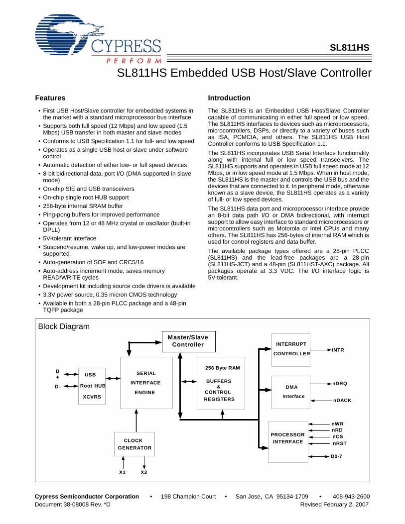
IntroductionThe SL811HS is an Embedded USB Host/Slave Controllercapable of communicating in either full speed or low speed.The SL811HS interfaces to devices such as microprocessors,microcontrollers, DSPs, or directly to a variety of buses suchas ISA, PCMCIA, and others. The SL811HS USB HostController conforms to USB Specification 1.1.The SL811HS incorporates USB Serial Interface functionalityalong with internal full or low speed transceivers. TheSL811HS supports and operates in USB full speed mode at 12Mbps, or in low speed mode at 1.5 Mbps. When in host mode,the SL811HS is the master and controls the USB bus and thedevices that are connected to it. In peripheral mode, otherwiseknown as a slave device, the SL811HS operates as a varietyof full- or low speed devices.The SL811HS data port and microprocessor interface providean 8-bit data path I/O or DMA bidirectional, with interruptsupport to allow easy interface to standard microprocessors ormicrocontrollers such as Motorola or Intel CPUs and manyothers. The SL811HS has 256-bytes of internal RAM which isused for control registers and data buffer.The available package types offered are a 28-pin PLCC(SL811HS) and the lead-free packages are a 28-pin(SL811HS-JCT) and a 48-pin (SL811HST-AXC) package. Allpackages operate at 3.3 VDC. The I/O interface logic is5V-tolerant.
X1 X2
D+
D-
INTR
nWRnRDnCSnRST
D0-7GENERATOR
USB
Root HUB
XCVRS
SERIAL
INTERFACE
ENGINE
256 Byte RAM
BUFFERS
CONTROLREGISTERS
INTERRUPT
CLOCK
&
CONTROLLER
PROCESSORINTERFACE
Master/SlaveController
nDRQ
nDACK
DMA
Interface
Block Diagram
Cypress Semiconductor Corporation • 198 Champion Court • San Jose, CA 95134-1709 • 408-943-2600Document 38-08008 Rev. *D Revised February 2, 2007
SL811HS
Data Port, Microprocessor InterfaceThe SL811HS microprocessor interface provides an 8-bitbidirectional data path along with appropriate control lines tointerface to external processors or controllers. ProgrammedI/O or memory mapped I/O designs are supported through the8-bit interface, chip select, read and write input strobes, and asingle address line, A0.Access to memory and control register space is a simple twostep process, requiring an address Write with A0 = ’0’, followedby a register/memory Read or Write cycle with address line A0= ’1’. In addition, a DMA bidirectional interface in slave mode isavailable with handshake signals such as nDRQ, nDACK,nWR, nRD, nCS and INTRQ. The SL811HS WRITE or READ operation terminates wheneither nWR or nCS goes inactive. For devices interfacing tothe SL811HS that deactivate the Chip Select nCS before theWrite nWR, the data hold timing must be measured from thenCS and will be the same value as specified. Therefore, bothIntel®- and Motorola-type CPUs work easily with the SL811HSwithout any external glue logic requirements.
DMA Controller (slave mode only)In applications that require transfers of large amounts of datasuch as scanner interfaces, the SL811HS provides a DMA in-terface. This interface supports DMA READ or WRITE trans-fers to the SL811HS internal RAM buffer, it is done through themicroprocessor data bus via two control lines (nDRQ - DataRequest and nDACK - Data Acknowledge), along with thenWR line and controls the data flow into the SL811HS. TheSL811HS has a count register that allows selection of pro-grammable block sizes for DMA transfer. The control signals,both nDRQ and nDACK, are designed for compatibility withstandard DMA interfaces.
Interrupt ControllerThe SL811HS interrupt controller provides a single outputsignal (INTRQ) that is activated by a number of programmableevents that may occur as result of USB activity. Control andstatus registers are provided to allow the user to select singleor multiple events, which generate an interrupt (assert INTRQ)and let the user view interrupt status. The interrupts arecleared by writing to the Interrupt Status Register.
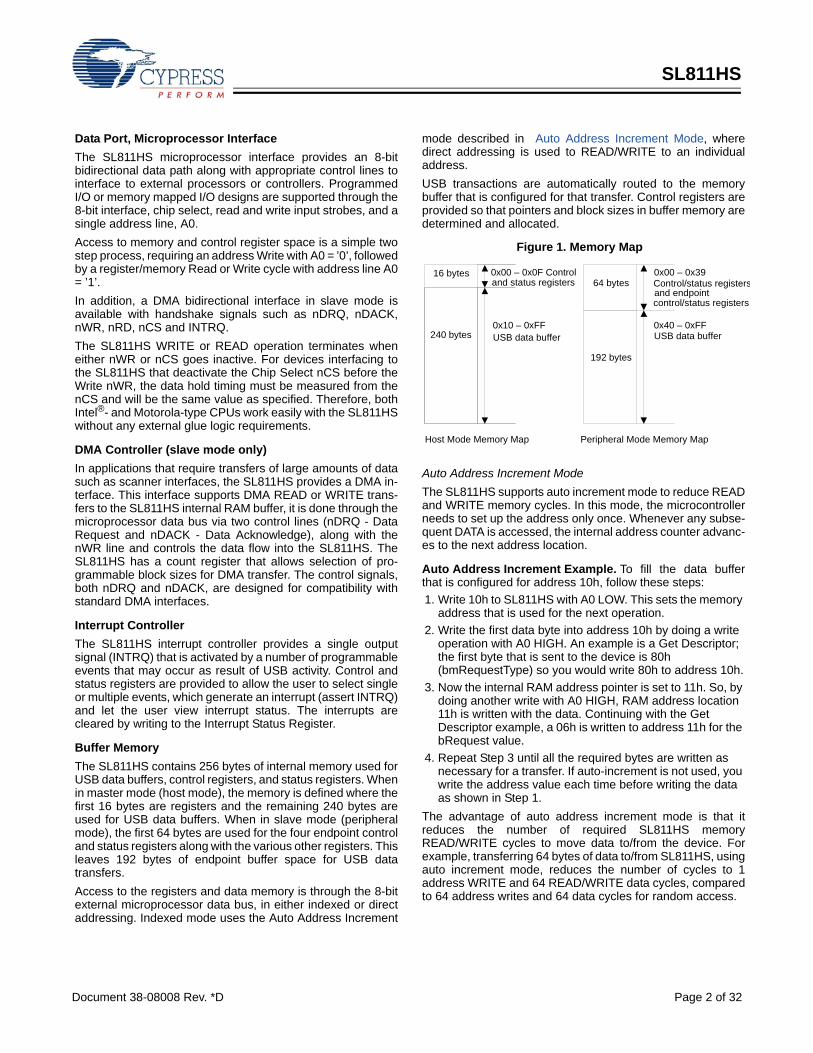
Buffer MemoryThe SL811HS contains 256 bytes of internal memory used forUSB data buffers, control registers, and status registers. Whenin master mode (host mode), the memory is defined where thefirst 16 bytes are registers and the remaining 240 bytes areused for USB data buffers. When in slave mode (peripheralmode), the first 64 bytes are used for the four endpoint controland status registers along with the various other registers. Thisleaves 192 bytes of endpoint buffer space for USB datatransfers.Access to the registers and data memory is through the 8-bitexternal microprocessor data bus, in either indexed or directaddressing. Indexed mode uses the Auto Address Increment
mode described in Auto Address Increment Mode, wheredirect addressing is used to READ/WRITE to an individualaddress. USB transactions are automatically routed to the memorybuffer that is configured for that transfer. Control registers areprovided so that pointers and block sizes in buffer memory aredetermined and allocated.
Auto Address Increment ModeThe SL811HS supports auto increment mode to reduce READand WRITE memory cycles. In this mode, the microcontrollerneeds to set up the address only once. Whenever any subse-quent DATA is accessed, the internal address counter advanc-es to the next address location.
Auto Address Increment Example. To fill the data bufferthat is configured for address 10h, follow these steps:1. Write 10h to SL811HS with A0 LOW. This sets the memory
address that is used for the next operation.2. Write the first data byte into address 10h by doing a write
operation with A0 HIGH. An example is a Get Descriptor; the first byte that is sent to the device is 80h (bmRequestType) so you would write 80h to address 10h.
3. Now the internal RAM address pointer is set to 11h. So, by doing another write with A0 HIGH, RAM address location 11h is written with the data. Continuing with the Get Descriptor example, a 06h is written to address 11h for the bRequest value.
4. Repeat Step 3 until all the required bytes are written as necessary for a transfer. If auto-increment is not used, you write the address value each time before writing the data as shown in Step 1.
The advantage of auto address increment mode is that itreduces the number of required SL811HS memoryREAD/WRITE cycles to move data to/from the device. Forexample, transferring 64 bytes of data to/from SL811HS, usingauto increment mode, reduces the number of cycles to 1address WRITE and 64 READ/WRITE data cycles, comparedto 64 address writes and 64 data cycles for random access.
0x00 – 0x0F Controland status registers
0x10 – 0xFFUSB data buffer240 bytes
16 bytes 0x00 – 0x39Control/status registersand endpointcontrol/status registers
0x40 – 0xFFUSB data buffer
192 bytes
64 bytes
Host Mode Memory Map Peripheral Mode Memory Map
Figure 1. Memory Map
Document 38-08008 Rev. *D Page 2 of 32
SL811HS
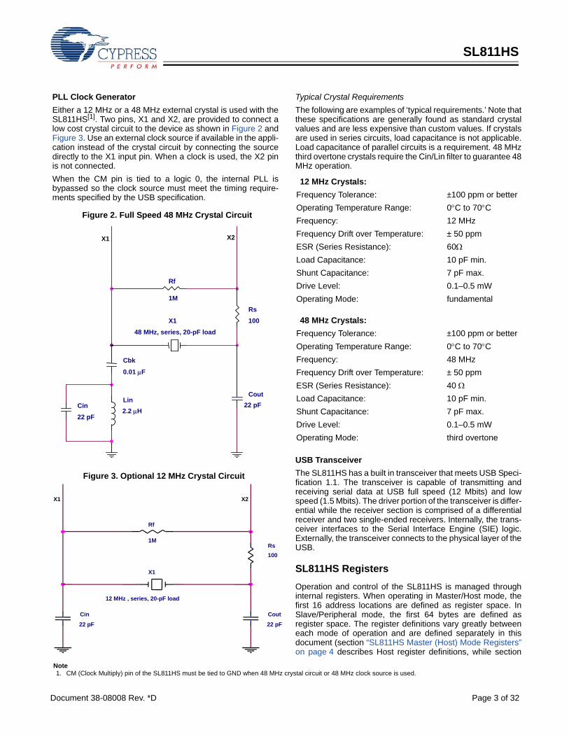
PLL Clock GeneratorEither a 12 MHz or a 48 MHz external crystal is used with theSL811HS[1]. Two pins, X1 and X2, are provided to connect alow cost crystal circuit to the device as shown in Figure 2 andFigure 3. Use an external clock source if available in the appli-cation instead of the crystal circuit by connecting the sourcedirectly to the X1 input pin. When a clock is used, the X2 pinis not connected. When the CM pin is tied to a logic 0, the internal PLL isbypassed so the clock source must meet the timing require-ments specified by the USB specification.
Typical Crystal RequirementsThe following are examples of ‘typical requirements.’ Note thatthese specifications are generally found as standard crystalvalues and are less expensive than custom values. If crystalsare used in series circuits, load capacitance is not applicable.Load capacitance of parallel circuits is a requirement. 48 MHzthird overtone crystals require the Cin/Lin filter to guarantee 48MHz operation.
USB TransceiverThe SL811HS has a built in transceiver that meets USB Speci-fication 1.1. The transceiver is capable of transmitting andreceiving serial data at USB full speed (12 Mbits) and lowspeed (1.5 Mbits). The driver portion of the transceiver is differ-ential while the receiver section is comprised of a differentialreceiver and two single-ended receivers. Internally, the trans-ceiver interfaces to the Serial Interface Engine (SIE) logic.Externally, the transceiver connects to the physical layer of theUSB.
SL811HS RegistersOperation and control of the SL811HS is managed throughinternal registers. When operating in Master/Host mode, thefirst 16 address locations are defined as register space. InSlave/Peripheral mode, the first 64 bytes are defined asregister space. The register definitions vary greatly betweeneach mode of operation and are defined separately in thisdocument (section “SL811HS Master (Host) Mode Registers”on page 4 describes Host register definitions, while section
Note1. CM (Clock Multiply) pin of the SL811HS must be tied to GND when 48 MHz crystal circuit or 48 MHz clock source is used.
Cbk 0.01 μF
Rs100X1
48 MHz, series, 20-pF load
Cout22 pF
Rf
1M
X2
Cin 22 pF
Lin 2.2 μH
X1
Figure 2. Full Speed 48 MHz Crystal Circuit
X1
12 MHz , series, 20-pF load
Rf
1M
Cin
22 pF
Cout 22 pF
Rs 100
X2X1
Figure 3. Optional 12 MHz Crystal Circuit
12 MHz Crystals:Frequency Tolerance: ±100 ppm or betterOperating Temperature Range: 0°C to 70°CFrequency: 12 MHzFrequency Drift over Temperature: ± 50 ppmESR (Series Resistance): 60ΩLoad Capacitance: 10 pF min.Shunt Capacitance: 7 pF max.Drive Level: 0.1–0.5 mWOperating Mode: fundamental
48 MHz Crystals:Frequency Tolerance: ±100 ppm or betterOperating Temperature Range: 0°C to 70°CFrequency: 48 MHzFrequency Drift over Temperature: ± 50 ppmESR (Series Resistance): 40 ΩLoad Capacitance: 10 pF min.Shunt Capacitance: 7 pF max.Drive Level: 0.1–0.5 mWOperating Mode: third overtone
Document 38-08008 Rev. *D Page 3 of 32

SL811HS
“SL811HS Slave Mode Registers” on page 12 describes Slaveregister definitions). Access to the registers are through themicroprocessor interface similar to normal RAM accesses(see “Bus Interface Timing Requirements” on page 26) andprovide control and status information for USB transactions. Any write to control register 0FH enables the SL811HS fullfeatures bit. This is an internal bit of the SL811HS that enablesadditional features.Table 1 shows the memory map and register mapping of theSL811HS in master/host mode.
SL811HS Master (Host) Mode Registers
The registers in the SL811HS are divided into two majorgroups. The first group is referred to as USB Control registers.These registers enable and provide status for control of USBtransactions and data flow. The second group of registersprovides control and status for all other operations.
Register Values on Power Up and ResetThe following registers initialize to zero on power up and reset:
• USB-A/USB-B Host Control Register [00H, 08H] bit 0 only• Control Register 1 [05H]• USB Address Register [07H]• Current Data Set/Hardware Revision/SOF Counter LOW
Register [0EH]
All other register’s power up and reset in an unknown state andfirmware for initialization.
USB Control RegistersCommunication and data flow on the USB bus uses theSL811HS’ USB A-B Control registers. The SL811HS commu-nicates with any USB Device function and any specificendpoint via the USB-A or USB-B register sets. The USB A-B Host Control registers are used in an overlappedconfiguration to manage traffic on the USB bus. The USB HostControl register also provides a means to interrupt an externalCPU or microcontroller when one of the USB protocol transac-tions is completed. Table 1 and Table 2 show the two sets ofUSB Host Control registers, the ’A’ set and ’B’ set. The tworegister sets allow for overlapping operation. When one set ofparameters is being set up, the other is transferring. Oncompletion of a transfer to an endpoint, the next operation iscontrolled by the other register set. Note The USB-B register set is used only when SL811HSmode is enabled by initializing register 0FH.The SL811HS USB Host Control has two groups of fiveregisters each which map in the SL811HS memory space.These registers are defined in the following tables.
SL811HS Host Control Registers.
Table 1. SL811HS Master (Host) Register SummaryRegister Name
SL811HSSL811HS
(hex) Address USB-A Host Control Register 00hUSB-A Host Base Address 01hUSB-A Host Base Length 02hUSB-A Host PID, Device Endpoint (Write)/USB Status (Read)
03h
USB-A Host Device Address (Write)/Transfer Count (Read)
04h
Control Register 1 05hInterrupt Enable Register 06hReserved Register ReservedUSB-B Host Control Register 08hUSB-B Host Base Address 09hUSB-B Host Base Length 0AhUSB-B Host PID, Device Endpoint (Write)/USB Status (Read)
0Bh
USB-B Host Device Address (Write)/Transfer Count (Read)
0Ch
Status Register 0DhSOF Counter LOW (Write)/HW Revision Reg-ister (Read)
0Eh
SOF Counter HIGH and Control Register 2 0FhMemory Buffer 10H-FFh
Table 2. SL811HS Host Control Registers
Register Name SL811HSL811HS
(hex) AddressUSB-A Host Control Register 00hUSB-A Host Base Address 01hUSB-A Host Base Length 02hUSB-A Host PID, Device Endpoint (Write)/USB Status (Read)
03h
USB-A Host Device Address (Write)/Transfer Count (Read)
04h
USB-B Host Control Register 08hUSB-B Host Base Address 09hUSB-B Host Base Length 0AhUSB-B Host PID, Device Endpoint (Write)/USB Status (Read)
0Bh
USB-B Host Device Address (Write)/Transfer Count (Read)
0Ch
Document 38-08008 Rev. *D Page 4 of 32
SL811HS
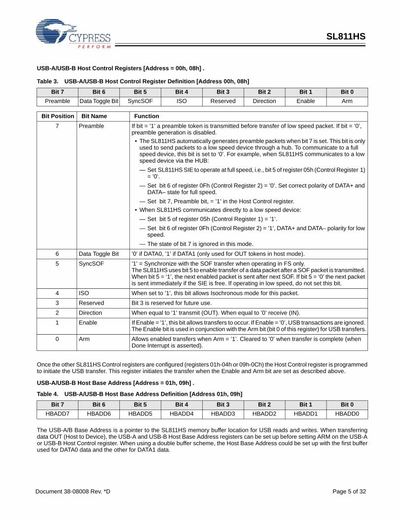
USB-A/USB-B Host Control Registers [Address = 00h, 08h] .
Once the other SL811HS Control registers are configured (registers 01h-04h or 09h-0Ch) the Host Control register is programmedto initiate the USB transfer. This register initiates the transfer when the Enable and Arm bit are set as described above.
USB-A/USB-B Host Base Address [Address = 01h, 09h] .
The USB-A/B Base Address is a pointer to the SL811HS memory buffer location for USB reads and writes. When transferringdata OUT (Host to Device), the USB-A and USB-B Host Base Address registers can be set up before setting ARM on the USB-Aor USB-B Host Control register. When using a double buffer scheme, the Host Base Address could be set up with the first bufferused for DATA0 data and the other for DATA1 data.
Table 3. USB-A/USB-B Host Control Register Definition [Address 00h, 08h]
Bit 7 Bit 6 Bit 5 Bit 4 Bit 3 Bit 2 Bit 1 Bit 0Preamble Data Toggle Bit SyncSOF ISO Reserved Direction Enable Arm
Bit Position Bit Name Function7 Preamble If bit = ’1’ a preamble token is transmitted before transfer of low speed packet. If bit = ’0’,
preamble generation is disabled.• The SL811HS automatically generates preamble packets when bit 7 is set. This bit is only
used to send packets to a low speed device through a hub. To communicate to a full speed device, this bit is set to ‘0’. For example, when SL811HS communicates to a low speed device via the HUB:— Set SL811HS SIE to operate at full speed, i.e., bit 5 of register 05h (Control Register 1)
= ’0’. — Set bit 6 of register 0Fh (Control Register 2) = ’0’. Set correct polarity of DATA+ and
DATA– state for full speed.— Set bit 7, Preamble bit, = ’1’ in the Host Control register.
• When SL811HS communicates directly to a low speed device:— Set bit 5 of register 05h (Control Register 1) = ’1’.— Set bit 6 of register 0Fh (Control Register 2) = ’1’, DATA+ and DATA– polarity for low
speed.— The state of bit 7 is ignored in this mode.
6 Data Toggle Bit ’0’ if DATA0, ’1’ if DATA1 (only used for OUT tokens in host mode).
5 SyncSOF ’1’ = Synchronize with the SOF transfer when operating in FS only.The SL811HS uses bit 5 to enable transfer of a data packet after a SOF packet is transmitted. When bit 5 = ‘1’, the next enabled packet is sent after next SOF. If bit 5 = ‘0’ the next packet is sent immediately if the SIE is free. If operating in low speed, do not set this bit.
4 ISO When set to ’1’, this bit allows Isochronous mode for this packet.
3 Reserved Bit 3 is reserved for future use.
2 Direction When equal to ’1’ transmit (OUT). When equal to ’0’ receive (IN).
1 Enable If Enable = ’1’, this bit allows transfers to occur. If Enable = ’0’, USB transactions are ignored. The Enable bit is used in conjunction with the Arm bit (bit 0 of this register) for USB transfers.
0 Arm Allows enabled transfers when Arm = ’1’. Cleared to ’0’ when transfer is complete (when Done Interrupt is asserted).
Table 4. USB-A/USB-B Host Base Address Definition [Address 01h, 09h]
Bit 7 Bit 6 Bit 5 Bit 4 Bit 3 Bit 2 Bit 1 Bit 0HBADD7 HBADD6 HBADD5 HBADD4 HBADD3 HBADD2 HBADD1 HBADD0
Document 38-08008 Rev. *D Page 5 of 32
SL811HS
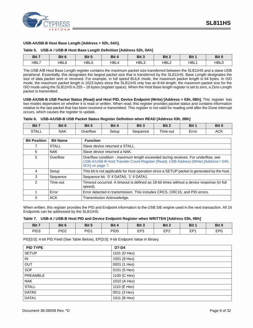
USB-A/USB-B Host Base Length [Address = 02h, 0Ah].
The USB A/B Host Base Length register contains the maximum packet size transferred between the SL811HS and a slave USBperipheral. Essentially, this designates the largest packet size that is transferred by the SL811HS. Base Length designates thesize of data packet sent or received. For example, in full speed BULK mode, the maximum packet length is 64 bytes. In ISOmode, the maximum packet length is 1023 bytes since the SL811HS only has an 8-bit length; the maximum packet size for theISO mode using the SL811HS is 255 – 16 bytes (register space). When the Host Base length register is set to zero, a Zero-Lengthpacket is transmitted.
USB-A/USB-B USB Packet Status (Read) and Host PID, Device Endpoint (Write) [Address = 03h, 0Bh]. This register hastwo modes dependent on whether it is read or written. When read, this register provides packet status and contains informationrelative to the last packet that has been received or transmitted. This register is not valid for reading until after the Done interruptoccurs, which causes the register to update.
When written, this register provides the PID and Endpoint information to the USB SIE engine used in the next transaction. All 16Endpoints can be addressed by the SL811HS.
PID[3:0]: 4-bit PID Field (See Table Below), EP[3:0]: 4-bit Endpoint Value in Binary.
Table 5. USB-A / USB-B Host Base Length Definition [Address 02h, 0Ah]
Bit 7 Bit 6 Bit 5 Bit 4 Bit 3 Bit 2 Bit 1 Bit 0HBL7 HBL6 HBL5 HBL4 HBL3 HBL2 HBL1 HBL0
Table 6. USB-A/USB-B USB Packet Status Register Definition when READ [Address 03h, 0Bh]
Bit 7 Bit 6 Bit 5 Bit 4 Bit 3 Bit 2 Bit 1 Bit 0STALL NAK Overflow Setup Sequence Time-out Error ACK
Bit Position Bit Name Function7 STALL Slave device returned a STALL.6 NAK Slave device returned a NAK.5 Overflow Overflow condition - maximum length exceeded during receives. For underflow, see
USB-A/USB-B Host Transfer Count Register (Read), USB Address (Write) [Address = 04h, 0Ch] on page 7.
4 Setup This bit is not applicable for Host operation since a SETUP packet is generated by the host.3 Sequence Sequence bit. ’0’ if DATA0, ’1’ if DATA1.2 Time-out Timeout occurred. A timeout is defined as 18-bit times without a device response (in full
speed).1 Error Error detected in transmission. This includes CRC5, CRC16, and PID errors. 0 ACK Transmission Acknowledge.
Table 7. USB-A / USB-B Host PID and Device Endpoint Register when WRITTEN [Address 03h, 0Bh]
Bit 7 Bit 6 Bit 5 Bit 4 Bit 3 Bit 2 Bit 1 Bit 0PID3 PID2 PID1 PID0 EP3 EP2 EP1 EP0
PID TYPE D7-D4SETUP 1101 (D Hex)IN 1001 (9 Hex)OUT 0001 (1 Hex)SOF 0101 (5 Hex)PREAMBLE 1100 (C Hex)NAK 1010 (A Hex)STALL 1110 (E Hex)DATA0 0011 (3 Hex)DATA1 1011 (B Hex)
Document 38-08008 Rev. *D Page 6 of 32
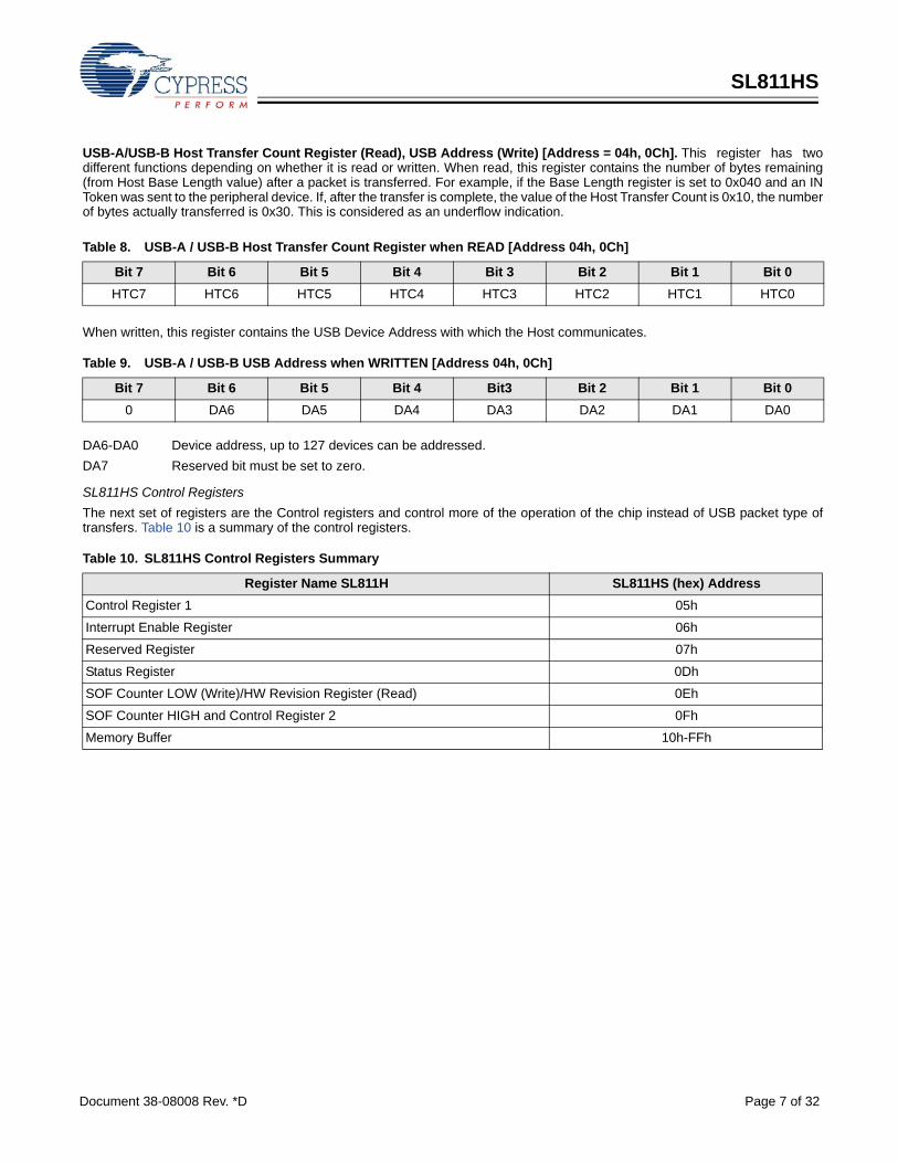
SL811HS
USB-A/USB-B Host Transfer Count Register (Read), USB Address (Write) [Address = 04h, 0Ch]. This register has twodifferent functions depending on whether it is read or written. When read, this register contains the number of bytes remaining(from Host Base Length value) after a packet is transferred. For example, if the Base Length register is set to 0x040 and an INToken was sent to the peripheral device. If, after the transfer is complete, the value of the Host Transfer Count is 0x10, the numberof bytes actually transferred is 0x30. This is considered as an underflow indication.
When written, this register contains the USB Device Address with which the Host communicates.
DA6-DA0 Device address, up to 127 devices can be addressed.DA7 Reserved bit must be set to zero.
SL811HS Control Registers The next set of registers are the Control registers and control more of the operation of the chip instead of USB packet type oftransfers. Table 10 is a summary of the control registers.
Table 8. USB-A / USB-B Host Transfer Count Register when READ [Address 04h, 0Ch]
Bit 7 Bit 6 Bit 5 Bit 4 Bit 3 Bit 2 Bit 1 Bit 0HTC7 HTC6 HTC5 HTC4 HTC3 HTC2 HTC1 HTC0
Table 9. USB-A / USB-B USB Address when WRITTEN [Address 04h, 0Ch]
Bit 7 Bit 6 Bit 5 Bit 4 Bit3 Bit 2 Bit 1 Bit 00 DA6 DA5 DA4 DA3 DA2 DA1 DA0
Table 10. SL811HS Control Registers Summary
Register Name SL811H SL811HS (hex) Address Control Register 1 05h
Interrupt Enable Register 06h
Reserved Register 07h
Status Register 0Dh
SOF Counter LOW (Write)/HW Revision Register (Read) 0Eh
SOF Counter HIGH and Control Register 2 0Fh
Memory Buffer 10h-FFh
Document 38-08008 Rev. *D Page 7 of 32
SL811HS
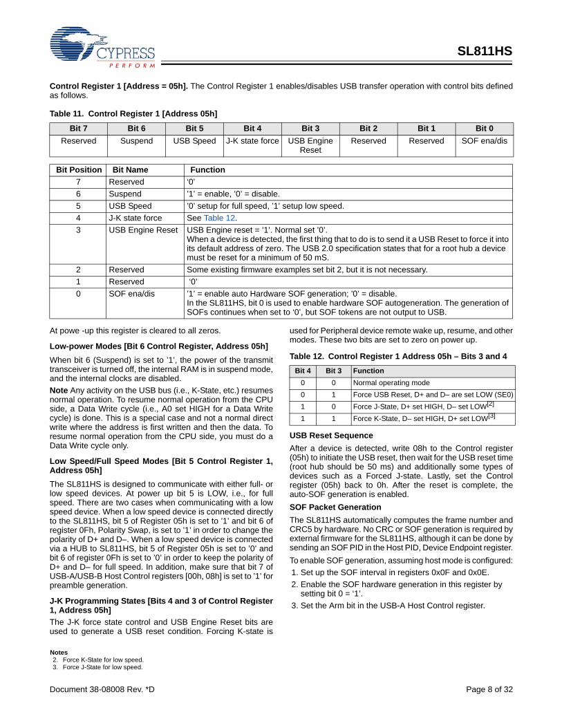
Control Register 1 [Address = 05h]. The Control Register 1 enables/disables USB transfer operation with control bits definedas follows.
At powe -up this register is cleared to all zeros.
Low-power Modes [Bit 6 Control Register, Address 05h]When bit 6 (Suspend) is set to ’1’, the power of the transmittransceiver is turned off, the internal RAM is in suspend mode,and the internal clocks are disabled. Note Any activity on the USB bus (i.e., K-State, etc.) resumesnormal operation. To resume normal operation from the CPUside, a Data Write cycle (i.e., A0 set HIGH for a Data Writecycle) is done. This is a special case and not a normal directwrite where the address is first written and then the data. Toresume normal operation from the CPU side, you must do aData Write cycle only.
Low Speed/Full Speed Modes [Bit 5 Control Register 1,Address 05h]The SL811HS is designed to communicate with either full- orlow speed devices. At power up bit 5 is LOW, i.e., for fullspeed. There are two cases when communicating with a lowspeed device. When a low speed device is connected directlyto the SL811HS, bit 5 of Register 05h is set to ’1’ and bit 6 ofregister 0Fh, Polarity Swap, is set to ’1’ in order to change thepolarity of D+ and D–. When a low speed device is connectedvia a HUB to SL811HS, bit 5 of Register 05h is set to ’0’ andbit 6 of register 0Fh is set to ’0’ in order to keep the polarity ofD+ and D– for full speed. In addition, make sure that bit 7 ofUSB-A/USB-B Host Control registers [00h, 08h] is set to ’1’ forpreamble generation.
J-K Programming States [Bits 4 and 3 of Control Register1, Address 05h]The J-K force state control and USB Engine Reset bits areused to generate a USB reset condition. Forcing K-state is
used for Peripheral device remote wake up, resume, and othermodes. These two bits are set to zero on power up.
USB Reset Sequence After a device is detected, write 08h to the Control register(05h) to initiate the USB reset, then wait for the USB reset time(root hub should be 50 ms) and additionally some types ofdevices such as a Forced J-state. Lastly, set the Controlregister (05h) back to 0h. After the reset is complete, theauto-SOF generation is enabled.SOF Packet GenerationThe SL811HS automatically computes the frame number andCRC5 by hardware. No CRC or SOF generation is required byexternal firmware for the SL811HS, although it can be done bysending an SOF PID in the Host PID, Device Endpoint register.To enable SOF generation, assuming host mode is configured:1. Set up the SOF interval in registers 0x0F and 0x0E.2. Enable the SOF hardware generation in this register by
setting bit 0 = ‘1’.3. Set the Arm bit in the USB-A Host Control register.
Table 11. Control Register 1 [Address 05h]
Bit 7 Bit 6 Bit 5 Bit 4 Bit 3 Bit 2 Bit 1 Bit 0Reserved Suspend USB Speed J-K state force USB Engine
ResetReserved Reserved SOF ena/dis
Bit Position Bit Name Function7 Reserved ‘0’6 Suspend ’1’ = enable, ’0’ = disable.5 USB Speed ’0’ setup for full speed, ’1’ setup low speed.4 J-K state force See Table 12.3 USB Engine Reset USB Engine reset = ’1’. Normal set ’0’.
When a device is detected, the first thing that to do is to send it a USB Reset to force it into its default address of zero. The USB 2.0 specification states that for a root hub a device must be reset for a minimum of 50 mS.
2 Reserved Some existing firmware examples set bit 2, but it is not necessary.1 Reserved ‘0’0 SOF ena/dis ’1’ = enable auto Hardware SOF generation; ’0’ = disable.
In the SL811HS, bit 0 is used to enable hardware SOF autogeneration. The generation of SOFs continues when set to ‘0’, but SOF tokens are not output to USB.
Table 12. Control Register 1 Address 05h – Bits 3 and 4Bit 4 Bit 3 Function
0 0 Normal operating mode0 1 Force USB Reset, D+ and D– are set LOW (SE0)1 0 Force J-State, D+ set HIGH, D– set LOW[2]
1 1 Force K-State, D– set HIGH, D+ set LOW[3]
Notes2. Force K-State for low speed.3. Force J-State for low speed.
Document 38-08008 Rev. *D Page 8 of 32
SL811HS
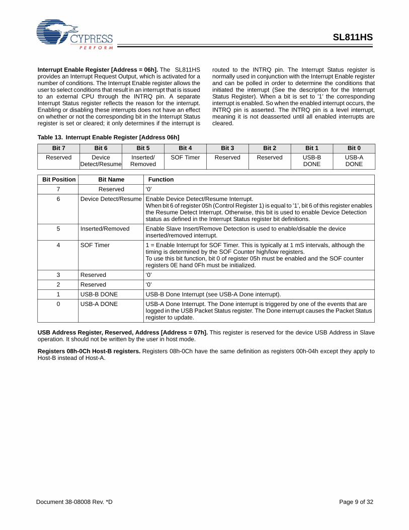
Interrupt Enable Register [Address = 06h]. The SL811HSprovides an Interrupt Request Output, which is activated for anumber of conditions. The Interrupt Enable register allows theuser to select conditions that result in an interrupt that is issuedto an external CPU through the INTRQ pin. A separateInterrupt Status register reflects the reason for the interrupt.Enabling or disabling these interrupts does not have an effecton whether or not the corresponding bit in the Interrupt Statusregister is set or cleared; it only determines if the interrupt is
routed to the INTRQ pin. The Interrupt Status register isnormally used in conjunction with the Interrupt Enable registerand can be polled in order to determine the conditions thatinitiated the interrupt (See the description for the InterruptStatus Register). When a bit is set to ’1’ the correspondinginterrupt is enabled. So when the enabled interrupt occurs, theINTRQ pin is asserted. The INTRQ pin is a level interrupt,meaning it is not deasserted until all enabled interrupts arecleared.
USB Address Register, Reserved, Address [Address = 07h]. This register is reserved for the device USB Address in Slaveoperation. It should not be written by the user in host mode.
Registers 08h-0Ch Host-B registers. Registers 08h-0Ch have the same definition as registers 00h-04h except they apply toHost-B instead of Host-A.
Table 13. Interrupt Enable Register [Address 06h]
Bit 7 Bit 6 Bit 5 Bit 4 Bit 3 Bit 2 Bit 1 Bit 0Reserved Device
Detect/ResumeInserted/Removed
SOF Timer Reserved Reserved USB-BDONE
USB-ADONE
Bit Position Bit Name Function7 Reserved ‘0’6 Device Detect/Resume Enable Device Detect/Resume Interrupt.
When bit 6 of register 05h (Control Register 1) is equal to ’1’, bit 6 of this register enables the Resume Detect Interrupt. Otherwise, this bit is used to enable Device Detection status as defined in the Interrupt Status register bit definitions.
5 Inserted/Removed Enable Slave Insert/Remove Detection is used to enable/disable the device inserted/removed interrupt.
4 SOF Timer 1 = Enable Interrupt for SOF Timer. This is typically at 1 mS intervals, although the timing is determined by the SOF Counter high/low registers.To use this bit function, bit 0 of register 05h must be enabled and the SOF counter registers 0E hand 0Fh must be initialized.
3 Reserved ‘0’2 Reserved ‘0’1 USB-B DONE USB-B Done Interrupt (see USB-A Done interrupt).0 USB-A DONE USB-A Done Interrupt. The Done interrupt is triggered by one of the events that are
logged in the USB Packet Status register. The Done interrupt causes the Packet Status register to update.
Document 38-08008 Rev. *D Page 9 of 32
SL811HS
Interrupt Status Register, Address [Address = 0Dh]. The Interrupt Status register is a READ/WRITE register providinginterrupt status. Interrupts are cleared by writing to this register. To clear a specific interrupt, the register is written with corre-sponding bit set to ’1’.
Current Data Set Register/Hardware Revision/SOF Counter LOW [Address = 0Eh]. This register has two modes. Readfrom this register indicates the current SL811HS silicon revision.
Writing to this register sets up auto generation of SOF to all connected peripherals. This counter is based on the 12 MHz clockand is not dependent on the crystal frequency. To set up a 1 ms timer interval, the software must set up both SOF counter registersto the proper values.
Table 14. Interrupt Status Register [Address 0Dh]
Bit 7 Bit 6 Bit 5 Bit 4 Bit 3 Bit 2 Bit 1 Bit 0D+ Device
Detect/ResumeInsert/Remove SOF timer Reserved Reserved USB-B USB-A
Bit Position Bit Name Function7 D+ Value of the Data+ pin.
Bit 7 provides continuous USB Data+ line status. Once it is determined that a device is inserted (as described below) with bits 5 and 6, bit 7 is used to detect if the inserted device is low speed (0) or full speed (1).
6 Device Detect/Resume Device Detect/Resume Interrupt.Bit 6 is shared between Device Detection status and Resume Detection interrupt. When bit-6 of register 05h is set to one, this bit is the Resume detection Interrupt bit. Otherwise, this bit is used to indicate the presence of a device, ’1’ = device ‘Not present’ and ’0’ = device ‘Present.’ In this mode, check this bit along with bit 5 to determine whether a device has been inserted or removed.
5 Insert/Remove Device Insert/Remove Detection.Bit 5 is provided to support USB cable insertion/removal for the SL811HS in host mode. This bit is set when a transition from SE0 to IDLE (device inserted) or from IDLE to SE0 (device removed) occurs on the bus.
4 SOF timer ‘1’ = Interrupt on SOF Timer.3 Reserved ‘0’2 Reserved ‘0’1 USB-B USB-B Done Interrupt. (See description in Interrupt Enable Register [address 06h].)0 USB-A USB-A Done Interrupt. (See description in Interrupt Enable Register [address 06h].)
Table 15. Hardware Revision when Read [Address 0Eh]
Bit 7 Bit 6 Bit 5 Bit 4 Bit 3 Bit 2 Bit 1 Bit 0Hardware Revision Reserved
Bit Position Bit Name Function7-4 Hardware Revision SL811HS rev1.2 Read = 1H; SL811HS rev1.5 Read = 2.3-2 Reserved Read is zero.1-0 Reserved Reserved for slave.
Document 38-08008 Rev. *D Page 10 of 32
SL811HS
Example: To set up SOF for 1 ms interval, SOF counter register 0Eh should be set to E0h.
SOF Counter High/Control Register 2 [Address = 0Fh]. When read, this register returns the value of the SOF counter dividedby 64. The software must use this register to determine the available bandwidth in the current frame before initiating any USBtransfer. In this way, the user is able to avoid babble conditions on the USB. For example, to determine the available bandwidthleft in a frame do the following.Maximum number of clock ticks in 1 ms time frame is 12000 (1 count per 12 MHz clock period, or approximately 84 ns.) The valueread back in Register 0FH is the (count × 64) × 84 ns = time remaining in current frame. USB bit time = one 12 MHz period. Value of register 0FH Available bit times left are between BBH 12000 bits to 11968 (187 × 64) bits BAH 11968 bits to 11904 (186 × 64) bitsNote: Any write to the 0Fh register clears the internal frame counter. Write register 0Fh at least once after power up. The internalframe counter is incremented after every SOF timer tick. The internal frame counter is an 11-bit counter, which is used to trackthe frame number. The frame number is incremented after each timer tick. Its contents are transmitted to the slave every milli-second in a SOF packet.
When writing to this register the bits definition are defined as follows.
Note Any write to Control register 0Fh enables the SL811HSfull features bit. This is an internal bit of the SL811HS thatenables additional features.The USB-B register set is used when SL811HS full feature bitis enabled. Example. To set up host to generate 1 ms SOF time:The register 0Fh contains the upper 6 bits of the SOF timer.Register 0Eh contains the lower 8 bits of the SOF timer. Thetimer is based on an internal 12 MHz clock and uses a counter,which counts down to zero from an initial value. To set the timerfor 1 ms time, the register 0Eh is loaded with value E0h andregister 0Fh (bits 0–5) is loaded with 2Eh. To start the timer,bit 0 of register 05h (Control Register 1) is set to ’1’, which
enables hardware SOF generation. To load both HIGH andLOW registers with the proper values, the user must follow thissequence:1. Write E0h to register 0Eh. This sets the lower byte of the
SOF counter2. Write AEh to register 0Fh, AEh configures the part for full
speed (no change of polarity) Host with bits 5–0 = 2Eh for upper portion of SOF counter.
3. Enable bit 0 in register 05h. This enables hardware gener-ation of SOF.
4. Set the ARM bit at address 00h. This starts the SOF gener-ation.
Table 16. SOF Counter LOW Address when Written [Address 0Eh]
Bit 7 Bit 6 Bit 5 Bit 4 Bit 3 Bit 2 Bit 1 Bit 0SOF7 SOF6 SOF5 SOF4 SOF3 SOF2 SOF1 SOF0
Table 17. SOF High Counter when Read [Address 0Fh]
Bit 7 Bit 6 Bit 5 Bit 4 Bit 3 Bit 2 Bit 1 Bit 0C13 C12 C11 C10 C9 C8 C7 C6
Table 18. Control Register 2 when Written [Address 0Fh]
Bit 7 Bit 6 Bit 5 Bit 4 Bit 3 Bit 2 Bit 1 Bit 0SL811HS
Master/Slave selection
SL811HS D+/D– Data
Polarity Swap
SOF High Counter Register
Bit Position Bit Name Function7 SL811HS Master/Slave selection Master = 1, Slave = 0.6 SL811HS D+/D– Data Polarity Swap ’1’ = change polarity (low speed)
’0’ = no change of polarity (full speed).5-0 SOF High Counter Register Write a value or read it back to SOF High Counter Register.
Document 38-08008 Rev. *D Page 11 of 32
SL811HS
SL811HS Slave Mode Registers
When in slave mode, the registers in the SL811HS are dividedinto two major groups. The first group contains Endpoint reg-isters that manage USB control transactions and data flow.The second group contains the USB Registers that provide thecontrol and status information for all other operations.
Endpoint RegistersCommunication and data flow on USB is implemented usingendpoints. These uniquely identifiable entities are theterminals of communication flow between a USB host andUSB devices. Each USB device is composed of a collection ofindependently operating endpoints. Each endpoint has aunique identifier, which is the Endpoint Number. For moreinformation, see USB Specification 1.1 section 5.3.1.The SL811HS supports four endpoints numbered 0–3.Endpoint 0 is the default pipe and is used to initialize andgenerically manipulate the device to configure the logicaldevice as the Default Control Pipe. It also provides access tothe device's configuration information, allows USB status andcontrol access, and supports control transfers. Endpoints 1–3 support Bulk, Isochronous, and Interrupttransfers. Endpoint 3 is supported by DMA. Each endpoint hastwo sets of registers—the 'A' set and the 'B' set. This allowsoverlapped operation where one set of parameters is set upand the other is transferring. Upon completion of a transfer toan endpoint, the ‘next data set’ bit indicates whether set 'A' orset 'B' is used next. The ‘armed’ bit of the next data setindicates whether the SL811HS is ready for the next transferwithout interruption.
Endpoints 0–3 Register AddressesEach endpoint set has a group of five registers that aremapped within the SL811HS memory. The register sets haveaddress assignments as shown in the following table.
For each endpoint set (starting at address Index = 0), theregisters are mapped as shown in the following table.
Table 19. SL811HS Slave/Peripheral Mode Register Summary
Register NameEndpoint specific register addresses
EP 0 – A EP 0 - B EP 1 – A EP 1 - B EP 2 - A EP 2 - B EP 3 - A EP 3 - BEP Control Register 00h 08h 10h 18h 20h 28h 30h 0x38EP Base Address Register 01h 09h 11h 19h 21h 29h 31h 0x39EP Base Length Register 02h 0Ah 12h 1Ah 22h 2Ah 0x32 0x3AEP Packet Status Register 03h 0Bh 13h 1Bh 23h 2Bh 0x33 0x3BEP Transfer Count Register 04h 0Ch 14h 1Ch 24h 2Ch 0x34 0x3C
Register Name Miscellaneous register addressesControl Register 1 05h Interrupt Status Register 0DhInterrupt Enable Register 06h Current Data Set Register 0EhUSB Address Register 07h Control Register 2 0FhSOF Low Register (read only) 15h Reserved 1Dh1FhSOF High Register (read only) 16h Reserved 25h-27hReserved 17h Reserved 2Dh-2FhDMA Total Count Low Register 35hDMA Total Count High Register 36hReserved 37hMemory Buffer 40h – FFh
Table 20. Endpoints 0–3 Register AddressesEndpoint Register Set Address (in Hex)
Endpoint 0 – a 00 - 04Endpoint 0 – b 08 - 0CEndpoint 1 – a 10 - 14Endpoint 1 – b 18 - 1CEndpoint 2 – a 20 - 24 Endpoint 2 – b 28 - 2CEndpoint 3 – a 30 - 34Endpoint 3 – b 38 - 3C
Table 21. Register Address MapEndpoint Register Sets
(for Endpoint n starting at register position Index=0)Index Endpoint n Control
Index + 1 Endpoint n Base AddressIndex + 2 Endpoint n Base LengthIndex + 3 Endpoint n Packet StatusIndex + 4 Endpoint n Transfer Count
Document 38-08008 Rev. *D Page 12 of 32
SL811HS
Endpoint Control Registers
Endpoint n Control Register [Address a = (EP# * 10h), b = (EP# * 10h)+8]. Each endpoint set has a Control register definedas follows:
Endpoint Base Address [Address a = (EP# * 10h)+1, b = (EP# * 10h)+9]]. Pointer to memory buffer location for USB readsand writes.
Endpoint Base Length [Address a = (EP# * 10h)+2, b = (EP# * 10h)+A]. The Endpoint Base Length is the maximum packetsize for IN/OUT transfers with the host. Essentially, this designates the largest packet size that is received by the SL811HS withan OUT transfer, or it designates the size of the data packet sent to the host for IN transfers.
Table 22. Endpoint Control Register [Address EP0a/b:00h/08h, EP1a/b:10h/18h, EP2a/b:20h/28h, EP3a/b:30h/38h]
7 6 5 4 3 2 1 0Reserved Sequence Send STALL ISO Next Data Set Direction Enable Arm
Bit Position Bit Name Function7 Reserved
6 Sequence Sequence bit. '0' if DATA0, '1' if DATA1.
5 Send STALL When set to ‘1’, sends Stall in response to next request on this endpoint.
4 ISO When set to '1', allows Isochronous mode for this endpoint.
3 Next Data Set '0' if next data set is ‘A’, '1' if next data set is 'B'.
2 Direction When Direction = '1', transmit to Host (IN). When Direction = '0', receive from Host (OUT).
1 Enable When Enable = '1', allows transfers for this endpoint. When set to ‘0’, USB transactions are ignored. If Enable = '1' and Arm = '0', the endpoint returns NAKs to USB transmissions.
0 Arm Allows enabled transfers when set =’1’. Clears to '0' when transfer is complete.
Table 23. Endpoint Base Address Reg [Address; EP0a/b:01h/09h, EP1a/b:11h/19h, EP2a/b:21h/29h, EP3a/b:31h/39h]
7 6 5 4 3 2 1 0EPxADD7 EPxADD6 EPxADD5 EPxADD4 EPxADD3 EPxADD2 EPxADD1 EPxADD0
Table 24. Endpoint Base Length Reg [Address EP0a/b:02h/0Ah, EP1a/b:12h/1Ah, EP2a/b:22h/2Ah, EP3a/b:32h/3Ah]
7 6 5 4 3 2 1 0EPxLEN7 EPxLEN6 EPxLEN5 EPxLEN4 EPxLEN3 EPxLEN2 EPxLEN1 EPxLEN0
Document 38-08008 Rev. *D Page 13 of 32
SL811HS
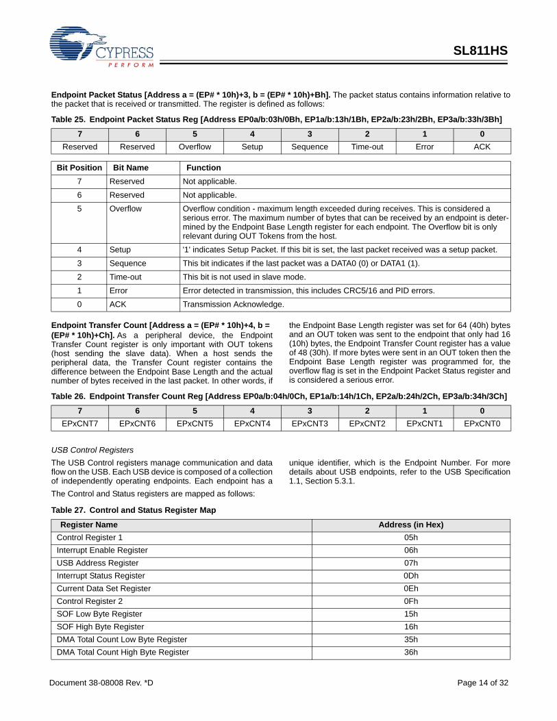
Endpoint Packet Status [Address a = (EP# * 10h)+3, b = (EP# * 10h)+Bh]. The packet status contains information relative tothe packet that is received or transmitted. The register is defined as follows:
Endpoint Transfer Count [Address a = (EP# * 10h)+4, b = (EP# * 10h)+Ch]. As a peripheral device, the EndpointTransfer Count register is only important with OUT tokens(host sending the slave data). When a host sends theperipheral data, the Transfer Count register contains thedifference between the Endpoint Base Length and the actualnumber of bytes received in the last packet. In other words, if
the Endpoint Base Length register was set for 64 (40h) bytesand an OUT token was sent to the endpoint that only had 16(10h) bytes, the Endpoint Transfer Count register has a valueof 48 (30h). If more bytes were sent in an OUT token then theEndpoint Base Length register was programmed for, theoverflow flag is set in the Endpoint Packet Status register andis considered a serious error.
USB Control Registers The USB Control registers manage communication and dataflow on the USB. Each USB device is composed of a collectionof independently operating endpoints. Each endpoint has a
unique identifier, which is the Endpoint Number. For moredetails about USB endpoints, refer to the USB Specification1.1, Section 5.3.1.
The Control and Status registers are mapped as follows:
Table 25. Endpoint Packet Status Reg [Address EP0a/b:03h/0Bh, EP1a/b:13h/1Bh, EP2a/b:23h/2Bh, EP3a/b:33h/3Bh]
7 6 5 4 3 2 1 0Reserved Reserved Overflow Setup Sequence Time-out Error ACK
Bit Position Bit Name Function7 Reserved Not applicable.
6 Reserved Not applicable.
5 Overflow Overflow condition - maximum length exceeded during receives. This is considered a serious error. The maximum number of bytes that can be received by an endpoint is deter-mined by the Endpoint Base Length register for each endpoint. The Overflow bit is only relevant during OUT Tokens from the host.
4 Setup '1' indicates Setup Packet. If this bit is set, the last packet received was a setup packet.
3 Sequence This bit indicates if the last packet was a DATA0 (0) or DATA1 (1).
2 Time-out This bit is not used in slave mode.
1 Error Error detected in transmission, this includes CRC5/16 and PID errors.
0 ACK Transmission Acknowledge.
Table 26. Endpoint Transfer Count Reg [Address EP0a/b:04h/0Ch, EP1a/b:14h/1Ch, EP2a/b:24h/2Ch, EP3a/b:34h/3Ch]
7 6 5 4 3 2 1 0EPxCNT7 EPxCNT6 EPxCNT5 EPxCNT4 EPxCNT3 EPxCNT2 EPxCNT1 EPxCNT0
Table 27. Control and Status Register Map
Register Name Address (in Hex)Control Register 1 05hInterrupt Enable Register 06hUSB Address Register 07hInterrupt Status Register 0DhCurrent Data Set Register 0EhControl Register 2 0FhSOF Low Byte Register 15hSOF High Byte Register 16hDMA Total Count Low Byte Register 35hDMA Total Count High Byte Register 36h
Document 38-08008 Rev. *D Page 14 of 32
SL811HS
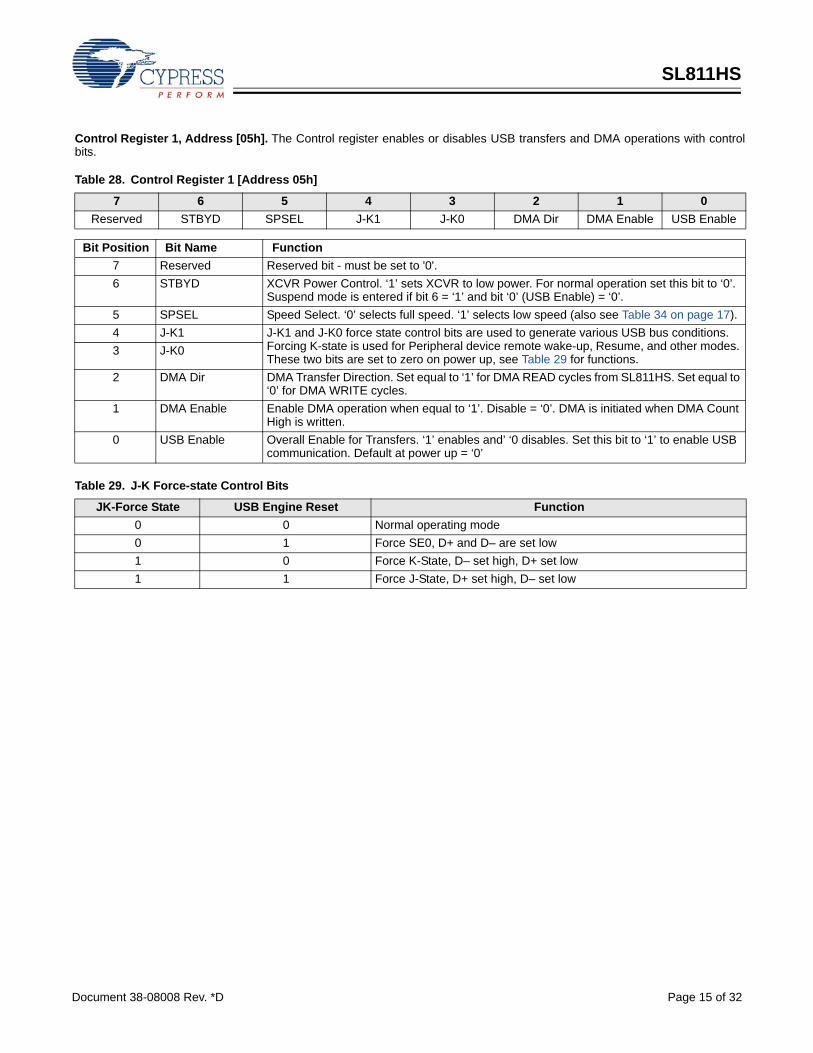
Control Register 1, Address [05h]. The Control register enables or disables USB transfers and DMA operations with controlbits.
Table 28. Control Register 1 [Address 05h]
7 6 5 4 3 2 1 0Reserved STBYD SPSEL J-K1 J-K0 DMA Dir DMA Enable USB Enable
Bit Position Bit Name Function7 Reserved Reserved bit - must be set to '0'.6 STBYD XCVR Power Control. ‘1’ sets XCVR to low power. For normal operation set this bit to ‘0’.
Suspend mode is entered if bit 6 = ‘1’ and bit ‘0’ (USB Enable) = ‘0’. 5 SPSEL Speed Select. ‘0’ selects full speed. ‘1’ selects low speed (also see Table 34 on page 17).4 J-K1 J-K1 and J-K0 force state control bits are used to generate various USB bus conditions.
Forcing K-state is used for Peripheral device remote wake-up, Resume, and other modes. These two bits are set to zero on power up, see Table 29 for functions.
3 J-K0
2 DMA Dir DMA Transfer Direction. Set equal to ‘1’ for DMA READ cycles from SL811HS. Set equal to ‘0’ for DMA WRITE cycles.
1 DMA Enable Enable DMA operation when equal to ‘1’. Disable = ‘0’. DMA is initiated when DMA Count High is written.
0 USB Enable Overall Enable for Transfers. ‘1’ enables and’ ‘0 disables. Set this bit to ‘1’ to enable USB communication. Default at power up = ‘0’
Table 29. J-K Force-state Control Bits
JK-Force State USB Engine Reset Function0 0 Normal operating mode0 1 Force SE0, D+ and D– are set low1 0 Force K-State, D– set high, D+ set low1 1 Force J-State, D+ set high, D– set low
Document 38-08008 Rev. *D Page 15 of 32
SL811HS
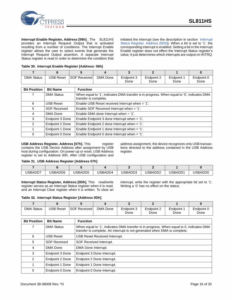
Interrupt Enable Register, Address [06h] . The SL811HSprovides an Interrupt Request Output that is activatedresulting from a number of conditions. The Interrupt Enableregister allows the user to select events that generate theInterrupt Request Output assertion. A separate InterruptStatus register is read in order to determine the condition that
initiated the interrupt (see the description in section InterruptStatus Register, Address [0Dh]). When a bit is set to ‘1’, thecorresponding interrupt is enabled. Setting a bit in the InterruptEnable register does not effect the Interrupt Status register’svalue; it just determines which interrupts are output on INTRQ.
USB Address Register, Address [07h]. This registercontains the USB Device Address after assignment by USBhost during configuration. On power up or reset, USB Addressregister is set to Address 00h. After USB configuration and
address assignment, the device recognizes only USB transac-tions directed to the address contained in the USB Addressregister.
Interrupt Status Register, Address [0Dh]. This read/writeregister serves as an Interrupt Status register when it is read,and an Interrupt Clear register when it is written. To clear an
interrupt, write the register with the appropriate bit set to ‘1’.Writing a ‘0’ has no effect on the status.
Table 30. Interrupt Enable Register [Address: 06h]
7 6 5 4 3 2 1 0DMA Status USB Reset SOF Received DMA Done Endpoint 3
DoneEndpoint 2
DoneEndpoint 1
DoneEndpoint 0
Done
Bit Position Bit Name Function7 DMA Status When equal to ‘1’, indicates DMA transfer is in progress. When equal to ‘0’, indicates DMA
transfer is complete.6 USB Reset Enable USB Reset received interrupt when = ‘1’.5 SOF Received Enable SOF Received Interrupt when = ‘1’.4 DMA Done Enable DMA done Interrupt when = ‘1’.3 Endpoint 3 Done Enable Endpoint 3 done Interrupt when = ‘1’.2 Endpoint 2 Done Enable Endpoint 2 done Interrupt when = ‘1’.1 Endpoint 1 Done Enable Endpoint 1 done Interrupt when = ‘1’.0 Endpoint 0 Done Enable Endpoint 0 done Interrupt when = ‘1’.
Table 31. USB Address Register [Address 07h]
7 6 5 4 3 2 1 0USBADD7 USBADD6 USBADD5 USBADD4 USBADD3 USBADD2 USBADD1 USBADD0
Table 32. Interrupt Status Register [Address 0Dh]
7 6 5 4 3 2 1 0DMA Status USB Reset SOF Received DMA Done Endpoint 3
DoneEndpoint 2
DoneEndpoint 1
DoneEndpoint 0
Done
Bit Position Bit Name Function7 DMA Status When equal to ‘1’, indicates DMA transfer is in progress. When equal to 0, indicates DMA
transfer is complete. An interrupt is not generated when DMA is complete.
6 USB Reset USB Reset Received Interrupt.
5 SOF Received SOF Received Interrupt.
4 DMA Done DMA Done Interrupt.
3 Endpoint 3 Done Endpoint 3 Done Interrupt.
2 Endpoint 2 Done Endpoint 2 Done Interrupt.
1 Endpoint 1 Done Endpoint 1 Done Interrupt.
0 Endpoint 0 Done Endpoint 0 Done Interrupt.
Document 38-08008 Rev. *D Page 16 of 32
SL811HS
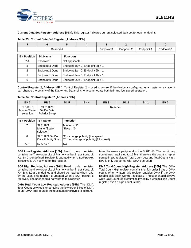
Current Data Set Register, Address [0Eh]. This register indicates current selected data set for each endpoint.
Control Register 2, Address [0Fh]. Control Register 2 is used to control if the device is configured as a master or a slave. Itcan change the polarity of the Data+ and Data- pins to accommodate both full- and low speed operation.
SOF Low Register, Address [15h]. Read only registercontains the 7 low order bits of Frame Number in positions: bit7:1. Bit 0 is undefined. Register is updated when a SOF packetis received. Do not write to this register.
SOF High Register, Address [16h]. Read only registercontains the 4 low order bits of Frame Number in positions: bit7:4. Bits 3:0 are undefined and should be masked when readby the user. This register is updated when a SOF packet isreceived. The user should not write to this register.
DMA Total Count Low Register, Address [35h]. The DMATotal Count Low register contains the low order 8 bits of DMAcount. DMA total count is the total number of bytes to be trans-
ferred between a peripheral to the SL811HS. The count maysometimes require up to 16 bits, therefore the count is repre-sented in two registers: Total Count Low and Total Count High.EP3 is only supported with DMA operation.
DMA Total Count High Register, Address [36h]. The DMATotal Count High register contains the high order 8 bits of DMAcount. When written, this register enables DMA if the DMAEnable bit is set in Control Register 1. The user should alwayswrite Low Count register first, followed by a write to High Countregister, even if high count is 00h.
Table 33. Current Data Set Register [Address 0Eh]
7 6 5 4 3 2 1 0Reserved Endpoint 3 Endpoint 2 Endpoint 1 Endpoint 0
Bit Position Bit Name Function7-4 Reserved Not applicable.
3 Endpoint 3 Done Endpoint 3a = 0, Endpoint 3b = 1.
2 Endpoint 2 Done Endpoint 2a = 0, Endpoint 2b = 1.
1 Endpoint 1 Done Endpoint 1a = 0, Endpoint 1b = 1.
0 Endpoint 0 Done Endpoint 0a = 0, Endpoint 0b = 1.
Table 34. Control Register 2 [Address 0Fh]
Bit 7 Bit 6 Bit 5 Bit 4 Bit 3 Bit 2 Bit 1 Bit 0SL811HS
Master/Slave selection
SL811HS D+/D– Data
Polarity Swap
Reserved
Bit Position Bit Name Function7 SL811HS
Master/Slave selection
Master = ‘1’Slave = ‘0’
6 SL811HS D+/D– Data Polarity Swap
’1’ = change polarity (low speed)’0’ = no change of polarity (full speed)
5-0 Reserved NA
Document 38-08008 Rev. *D Page 17 of 32

SL811HS
Physical ConnectionsThese parts are offered in both a 28-pin PLCC package and a 48-pin TQFP package. The 28-pin PLCC packages are theSL811HS and SL811HS-JCT. The 48-pin TQFP packages is the SL811HST-AXC.
28-Pin PLCC Physical Connections
28-Pin PLCC Pin Layout*See Table 35 on page 21 for Pin and Signal Description for Pins 2 and 3 in Host Mode.
28-Pin PLCC Mechanical Dimensions
12 28
nDACK*
nDRQ*
nRD
nWR
D7
D6
D5
D4
Gnd
D3
D2
D1
D0
Gnd
INTRQ
VDD1
nRST
VDD2
Gnd
nCS
DATA-
DATA+
VDD1
CLK/X1
X2
28 PLCC
A0 M/S
171615141312
11
10
9
8
7
6
5
4 3
25
24
22
21
20
19
18
27
26
23CM
Figure 4. 28-pin PLCC USB Host/Slave Controller — Pin Layout
Document 38-08008 Rev. *D Page 18 of 32

SL811HS
The diagram below illustrates a simple +3.3V voltage source.
Package Markings (28-pin PLCC)
YYWW = Date codeXXXX = Product codeX.X = Silicon revision number
+5V (USB)
GND
R1
+3.3 V (VDD)
Sample VDD Generator
45 Ohms
3.9v, 1N52288CT-Zener
2N2222
Figure 5. Sample VDD Generator
Part Number YYWW-X.X
XXXX
Document 38-08008 Rev. *D Page 19 of 32

SL811HS
48-Pin TQFP Physical Connections
48-Pin TQFP AXC Pin Layout
*See Table 35 on page 21 for Pin and Signal Description for Pins 43 and 44 in Host Mode.
48-Pin TQFP Mechanical Dimensions
Note4. NC. Indicates No Connection. NC Pins must be left unconnected.
48-Pin TQFP
1
12
13
2425
48
37
36
NC
NC NC
NC
NC
NCNC
NCNC NC
Data-
nRD NC
NC NC
NC
NC
nWR
nCS
CM
VDD1 Data+
VDD Clk/X1
X2
nRST
INTRQ GND
D0
D1
D2
D3
GND
D4
D5
D6
D7VDDM/SA0
nDACK* NC nDRQ*
USBGnd NC
NC
NC
NC
Figure 6. 48-Pin TQFP AXC USB Host/Slave Controller Pin Layout
[4]
Document 38-08008 Rev. *D Page 20 of 32
SL811HS
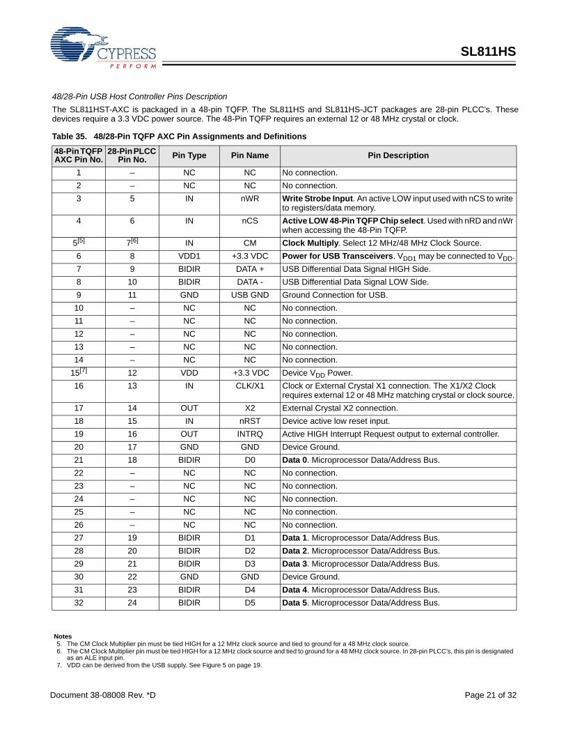
48/28-Pin USB Host Controller Pins DescriptionThe SL811HST-AXC is packaged in a 48-pin TQFP. The SL811HS and SL811HS-JCT packages are 28-pin PLCC’s. Thesedevices require a 3.3 VDC power source. The 48-Pin TQFP requires an external 12 or 48 MHz crystal or clock.
Table 35. 48/28-Pin TQFP AXC Pin Assignments and Definitions
48-Pin TQFP AXC Pin No.
28-Pin PLCC Pin No. Pin Type Pin Name Pin Description
1 – NC NC No connection.2 – NC NC No connection.3 5 IN nWR Write Strobe Input. An active LOW input used with nCS to write
to registers/data memory.4 6 IN nCS Active LOW 48-Pin TQFP Chip select. Used with nRD and nWr
when accessing the 48-Pin TQFP.5[5] 7[6] IN CM Clock Multiply. Select 12 MHz/48 MHz Clock Source.6 8 VDD1 +3.3 VDC Power for USB Transceivers. VDD1 may be connected to VDD.7 9 BIDIR DATA + USB Differential Data Signal HIGH Side.8 10 BIDIR DATA - USB Differential Data Signal LOW Side.9 11 GND USB GND Ground Connection for USB.10 – NC NC No connection.11 – NC NC No connection.12 – NC NC No connection.13 – NC NC No connection.14 – NC NC No connection.
15[7] 12 VDD +3.3 VDC Device VDD Power.16 13 IN CLK/X1 Clock or External Crystal X1 connection. The X1/X2 Clock
requires external 12 or 48 MHz matching crystal or clock source.17 14 OUT X2 External Crystal X2 connection.18 15 IN nRST Device active low reset input.19 16 OUT INTRQ Active HIGH Interrupt Request output to external controller.20 17 GND GND Device Ground.21 18 BIDIR D0 Data 0. Microprocessor Data/Address Bus.22 – NC NC No connection.23 – NC NC No connection.24 – NC NC No connection.25 – NC NC No connection.26 – NC NC No connection.27 19 BIDIR D1 Data 1. Microprocessor Data/Address Bus.28 20 BIDIR D2 Data 2. Microprocessor Data/Address Bus.29 21 BIDIR D3 Data 3. Microprocessor Data/Address Bus.30 22 GND GND Device Ground.31 23 BIDIR D4 Data 4. Microprocessor Data/Address Bus.32 24 BIDIR D5 Data 5. Microprocessor Data/Address Bus.
Notes5. The CM Clock Multiplier pin must be tied HIGH for a 12 MHz clock source and tied to ground for a 48 MHz clock source. 6. The CM Clock Multiplier pin must be tied HIGH for a 12 MHz clock source and tied to ground for a 48 MHz clock source. In 28-pin PLCC’s, this pin is designated
as an ALE input pin.7. VDD can be derived from the USB supply. See Figure 5 on page 19.
Document 38-08008 Rev. *D Page 21 of 32

SL811HS
33 25 BIDIR D6 Data 6. Microprocessor Data/Address Bus.34 – NC NC No connection.35 – NC NC No connection.36 – NC NC No connection.37 – NC NC No connection.38 – NC NC No connection.39 26 BIDIR D7 Data 7. Microprocessor Data/Address Bus. 40 27 IN M/S Master/Slave Mode Select. ’1’ selects Slave. ’0’ = Master.41 28[8] VDD +3.3 VDC Device VDD Power.
42[9] 1[9] IN A0 A0 = ’0’. Selects address pointer. Register A0 = ’1’. Selects data buffer or register.
43 2 IN nDACK DMA Acknowledge. An active LOW input used to interface to an external DMA controller. DMA is enabled only in slave mode. In host mode, the pin should be tied HIGH (logic ’1’).
44 3 OUT nDRQ DMA Request. An active LOW output used with an external DMA controller. nDRQ and nDACK form the handshake for DMA data transfers. In host mode, leave the pin unconnected.
45 4 IN nRD Read Strobe Input. An active LOW input used with nCS to read registers/data memory.
46 – NC NC No connection.47 – NC NC No connection.48 – NC NC No connection.
Table 35. 48/28-Pin TQFP AXC Pin Assignments and Definitions (continued)
48-Pin TQFP AXC Pin No.
28-Pin PLCC Pin No. Pin Type Pin Name Pin Description
Notes8. VDD can be derived from the USB supply. Figure 5 on page 19 shows a simple method to provide 3.3V/30 mA. Another option is to use a Torex Semiconductor,
Ltd. 3.3V SMD regulator (part number XC62HR3302MR).9. The A0 Address bit is used to access address register or data registers in I/O Mapped or Memory Mapped applications.
Document 38-08008 Rev. *D Page 22 of 32

SL811HS
Package Markings (48-Pin TQFP)
YYWW = Date codeXXXX = Product codeX.X = Silicon revision number
Part Number YYWW-X.X
XXXX
Document 38-08008 Rev. *D Page 23 of 32
SL811HS
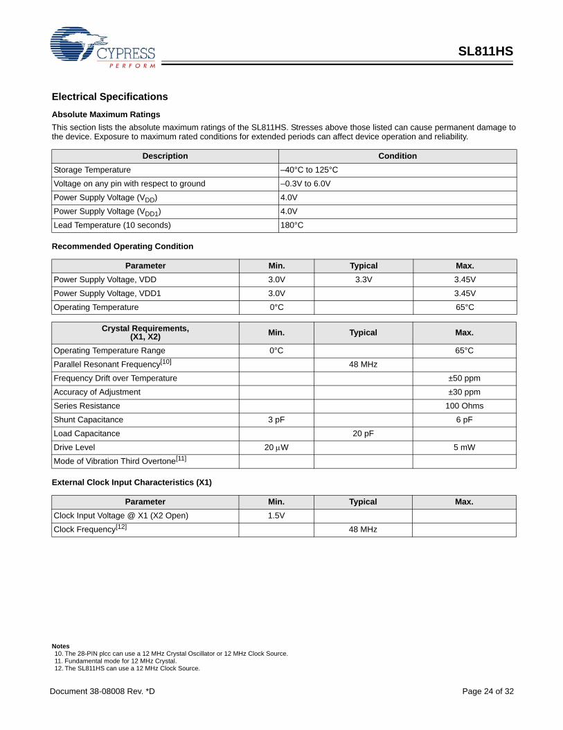
Electrical SpecificationsAbsolute Maximum RatingsThis section lists the absolute maximum ratings of the SL811HS. Stresses above those listed can cause permanent damage tothe device. Exposure to maximum rated conditions for extended periods can affect device operation and reliability.
Recommended Operating Condition
External Clock Input Characteristics (X1)
Description ConditionStorage Temperature –40°C to 125°C
Voltage on any pin with respect to ground –0.3V to 6.0V
Power Supply Voltage (VDD) 4.0V
Power Supply Voltage (VDD1) 4.0V
Lead Temperature (10 seconds) 180°C
Notes10. The 28-PIN plcc can use a 12 MHz Crystal Oscillator or 12 MHz Clock Source.11. Fundamental mode for 12 MHz Crystal.12. The SL811HS can use a 12 MHz Clock Source.
Parameter Min. Typical Max.Power Supply Voltage, VDD 3.0V 3.3V 3.45V
Power Supply Voltage, VDD1 3.0V 3.45V
Operating Temperature 0°C 65°C
Crystal Requirements,(X1, X2) Min. Typical Max.
Operating Temperature Range 0°C 65°C
Parallel Resonant Frequency[10] 48 MHz
Frequency Drift over Temperature ±50 ppm
Accuracy of Adjustment ±30 ppm
Series Resistance 100 Ohms
Shunt Capacitance 3 pF 6 pF
Load Capacitance 20 pF
Drive Level 20 μW 5 mW
Mode of Vibration Third Overtone[11]
Parameter Min. Typical Max.Clock Input Voltage @ X1 (X2 Open) 1.5V
Clock Frequency[12] 48 MHz
Document 38-08008 Rev. *D Page 24 of 32

SL811HS
DC Characteristics
USB Host Transceiver Characteristics
Every VDD pin, including USB VDD, must have a decouplingcapacitor to ensure clean VDD (free of high frequency noise)at the chip input point (pin) itself.The best way to do this is to connect a ceramic capacitor(0.1 μF, 6V) between the pin itself and a good ground. Keepcapacitor leads as short as possible. Use surface mount
capacitors with the shortest traces possible (the use of aground plane is strongly recommended).This product was tested as compliant to the USB-IF specifi-cation under the test identification number (TID) of 40000689and is listed on the USB-IF’s integrators list.
Parameter Description Min. Typ. Max.VIL Input Voltage LOW –0.3V 0.8V
VIH Input Voltage HIGH (5V Tolerant I/O) 2.0V 6.0V
VOL Output Voltage LOW (IOL = 4 mA) 0.4V
VOH Output Voltage HIGH (IOH = –4 mA) 2.4V
IOH Output Current HIGH 4 mA
IOL Output Current LOW 4 mA
ILL Input Leakage ±1 μA
CIN Input Capacitance 10 pF
ICC[13] Supply Current (VDD) inc USB @FS 21 mA 25 mA
ICCsus1[14] Supply Current (VDD) Suspend w/Clk & Pll Enb 4.2 mA 5 mA
ICCsus2[15] Supply Current (VDD) Suspend no Clk & Pll Dis 50 μA 60 μA
IUSB Supply Current (VDD1) 10 mA
IUSBSUS Transceiver Supply Current in Suspend 10 μA
Parameter Description Min. Typ.[16] Max.VIHYS Differential
Input Sensitivity (Data+, Data–)0.2V 200 mV
VUSBIH USB Input Voltage HIGH Driven 2.0V
VUSBIL USB Input Voltage LOW 0.8V
VUSBOH USB Output Voltage HIGH 2.0V
VUSBOL USB Output Voltage LOW 0.0V 0.3V
ZUSBH[17] Output Impedance HIGH STATE 36 Ohms 42 Ohms
ZUSBL[17] Output Impedance LOW STATE 36 Ohms 42 Ohms
IUSB Transceiver Supply p-p Current (3.3V) 10 mA@ FS
Notes13. ICC measurement includes USB Transceiver current (IUSB) operating at full speed. 14. ICCsus1 measured with 12 MHz Clock Input and Internal PLL enabled. Suspend set –(USB transceiver and internal Clocking disabled).15. ICCsus2 measured with external Clock, PLL disabled, and Suspend set. For absolute minimum current consumption, ensure that all inputs to the device are at
static logic level.16. All typical values are VDD = 3.3V and TAMB= 25°C.17. ZUSBX impedance values includes an external resistor of 24 Ohms ± 1% (SL811HS revision 1.2 requires external resistor values of 33 Ohms ±1%).
Document 38-08008 Rev. *D Page 25 of 32
SL811HS
Bus Interface Timing Requirements
I/O Write Cycle
Note nCS an be held LOW for multiple Write cycles provided nWR is cycled. Write Cycle Time for Auto Inc Mode Writes is 170ns minimum.
nWR
A0
D0-D7 DATA
twr
twahld
twdhld
twasu
twdsu twdsu twdhld
I/O Write Cycle to Register or Memory Buffer
Register or MemoryAddress
nCS
twcsu twshld
Tcscs See Note.
twrhigh
Parameter Description Min. Typ. Max.tWR Write pulse width 85 ns
tWCSU Chip select set-up to nWR LOW 0 ns
tWSHLD Chip select hold timeAfter nWR HIGH
0 ns
tWASU A0 address set-up time 85 ns
tWAHLD A0 address hold time 10 ns
tWDSU Data to Write HIGH set-up time 85 ns
tWDHLD Data hold time after Write HIGH 5 ns
tCSCS nCS inactive to nCS* asserted 85 ns
tWRHIGH NWR HIGH 85 ns
Document 38-08008 Rev. *D Page 26 of 32
SL811HS
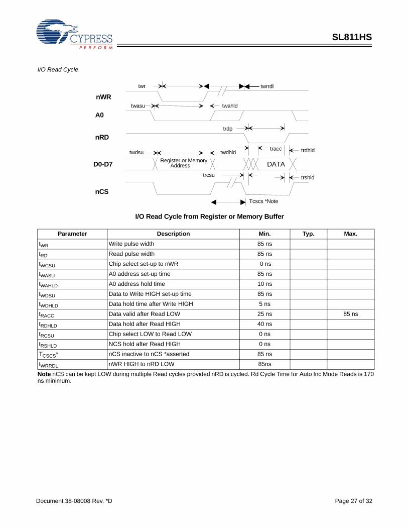
I/O Read Cycle
Note nCS can be kept LOW during multiple Read cycles provided nRD is cycled. Rd Cycle Time for Auto Inc Mode Reads is 170ns minimum.
nRD
A0
D0-D7 DATA
twr
twahld
twdhld
twasu
twdsu trdhld
I/O Read Cycle from Register or Memory Buffer
Register or MemoryAddress
trdp
nWR
trshld trcsu
nCS
tracc
Tcscs *Note
twrrdl
Parameter Description Min. Typ. Max.tWR Write pulse width 85 ns
tRD Read pulse width 85 ns
tWCSU Chip select set-up to nWR 0 ns
tWASU A0 address set-up time 85 ns
tWAHLD A0 address hold time 10 ns
tWDSU Data to Write HIGH set-up time 85 ns
tWDHLD Data hold time after Write HIGH 5 ns
tRACC Data valid after Read LOW 25 ns 85 ns
tRDHLD Data hold after Read HIGH 40 ns
tRCSU Chip select LOW to Read LOW 0 ns
tRSHLD NCS hold after Read HIGH 0 ns
TCSCS* nCS inactive to nCS *asserted 85 ns
tWRRDL nWR HIGH to nRD LOW 85ns
Document 38-08008 Rev. *D Page 27 of 32
SL811HS
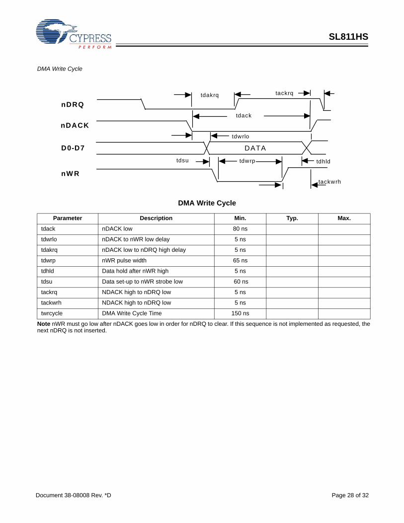
DMA Write Cycle
Note nWR must go low after nDACK goes low in order for nDRQ to clear. If this sequence is not implemented as requested, thenext nDRQ is not inserted.
Parameter Description Min. Typ. Max.
tdack nDACK low 80 ns
tdwrlo nDACK to nWR low delay 5 ns
tdakrq nDACK low to nDRQ high delay 5 ns
tdwrp nWR pulse width 65 ns
tdhld Data hold after nWR high 5 ns
tdsu Data set-up to nWR strobe low 60 ns
tackrq NDACK high to nDRQ low 5 ns
tackwrh NDACK high to nDRQ low 5 ns
twrcycle DMA Write Cycle Time 150 ns
nDRQ
nDACK
D0-D7 DATA
nW R
SL811 DMA W RITE CYCLE TIMING
tdwrp tdsu
tdack
tdhld
tdwrlo
tackwrh
tdakrq tackrq
DMA Write Cycle
Document 38-08008 Rev. *D Page 28 of 32
SL811HS
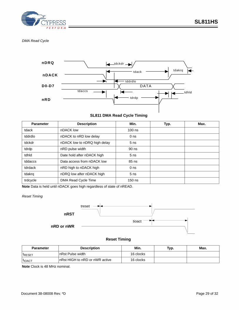
DMA Read Cycle
Note Data is held until nDACK goes high regardless of state of nREAD.
Reset Timing
Note Clock is 48 MHz nominal.
Parameter Description Min. Typ. Max.
tdack nDACK low 100 ns
tddrdlo nDACK to nRD low delay 0 ns
tdckdr nDACK low to nDRQ high delay 5 ns
tdrdp nRD pulse width 90 ns
tdhld Date hold after nDACK high 5 ns
tddaccs Data access from nDACK low 85 ns
tdrdack nRD high to nDACK high 0 ns
tdakrq nDRQ low after nDACK high 5 ns
trdcycle DMA Read Cycle Time 150 ns
nDRQ
nDACK
D0-D7 DATA
nRD
SL811 DMA READ CYCLE TIM ING
tdrdp
tdaccs
tdack
tdhld
tddrdlo
tdckdr
tdakrq
SL811 DMA Read Cycle Timing
nRST
treset
nRD or nWR tioact
Reset Timing
Parameter Description Min. Typ. Max.tRESET nRst Pulse width 16 clocks
tIOACT nRst HIGH to nRD or nWR active 16 clocks
Document 38-08008 Rev. *D Page 29 of 32
SL811HS
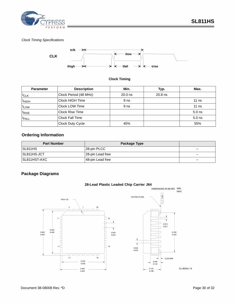
Clock Timing Specifications
Ordering Information
CLK
CLOCK TIMING
trisetfallthigh
tclktlow
Clock Timing
Parameter Description Min. Typ. Max.tCLK Clock Period (48 MHz) 20.0 ns 20.8 ns
tHIGH Clock HIGH Time 9 ns 11 ns
tLOW Clock LOW Time 9 ns 11 ns
tRISE Clock Rise Time 5.0 ns
tFALL Clock Fall Time 5.0 ns
Clock Duty Cycle 45% 55%
Part Number Package TypeSL811HS 28-pin PLCC –SL811HS-JCT 28-pin Lead free –SL811HST-AXC 48-pin Lead free –
Package Diagrams
DIMENSIONS IN INCHES MIN.MAX.
0.0450.055
0.026
0.013
0.032
0.021
0.020 MIN.
0.090
0.165
0.120
0.180
0.4850.495
0.4500.458
0.4580.450
0.4950.485
0.3900.430
4 26
1812
11
5
19
25
0.00
4
SEATING PLANE
1
PIN #1 ID
28-Lead Plastic Leaded Chip Carrier J64
51-85001-*A
Document 38-08008 Rev. *D Page 30 of 32

SL811HS
Intel is a registered trademark of Intel Corporation. Torex is a trademark of Torex Semiconductors, Ltd. SL811HS is a trademarkof Cypress Semiconductor Corporation. All product and company names mentioned in this document may be the trademarks oftheir respective holders.
Package Diagrams (continued)
48-Lead Thin Plastic Quad Flat Pack (7x7x1.4 mm) A48
51-85135-**
Document 38-08008 Rev. *D Page 31 of 32© Cypress Semiconductor Corporation, 2007. The information contained herein is subject to change without notice. Cypress Semiconductor Corporation assumes no responsibility for the useof any circuitry other than circuitry embodied in a Cypress product. Nor does it convey or imply any license under patent or other rights. Cypress products are not warranted nor intended to beused for medical, life support, life saving, critical control or safety applications, unless pursuant to an express written agreement with Cypress. Furthermore, Cypress does not authorize itsproducts for use as critical components in life-support systems where a malfunction or failure may reasonably be expected to result in significant injury to the user. The inclusion of Cypressproducts in life-support systems application implies that the manufacturer assumes all risk of such use and in doing so indemnifies Cypress against all charges.
SL811HS
Document History Page
Document Title: SL811HS Embedded USB Host/Slave ControllerDocument Number: 38-08008
REV. ECN NO. Issue Date Orig. of Change Description of Change
** 110850 12/14/01 BHA Converted to Cypress format from ScanLogic*A 112687 03/22/02 MUL 1) Changed power supply voltage to 4.0V in section 7.1
2) Changed value of twdsu in section 7.6.23) Changed max. power supply voltage to 3.45 V in section 7.24) Changed accuracy of adjustment in section 7.25) Changed bits 0 and 1 to reserved in section 5.3.86) Changed bit 2 to reserved in section 5.3.5 and 5.3.77) Changed bit 2 to reserved in section 5.3.18) Changed definition of bit 6 in section 5.3.5 & 5.3.79) Added section 5.1, Register Values on Power Up and Reset10) Changed bit description notes in section 5.3.711) Changed note about series termination resistors in section 7.512) Changed example in section 5.3.913) Changed J-K Programming States table in section 5.3.214) Added and removed comments for low-power modes in section 5.3.415) Removed sections specific to slave operation and SL11H16) Removed duplicate tables17) General formatting changes to section headings18) Fixed all part number references19) Added comments to section 7.5 and new definitions to section 2.0
*B 381894 See ECN VCS Went from single column to 2-column format. Combined information from SL811HS (38-08008) and SL811S/T (83-08009)
*C 464641 See ECN ARI Added lead free part numbers to new section Ordering Information and corrected references made to these parts. Corrected grammar. Added compliance statement in section USB Host Transceiver Characteristics.
*D 749518 See ECN ARI Implemented the new template. Changed Figure 4. Labels on pins 2 and 3 were swapped; this has been corrected. Combined the 48-pin TQFP AXC Pin Assignment and Definition table with the 28-pin PLCC Pin Assignment and Definition table. Removed all instances of SL811HST-AC. Corrected the variables. Removed references to the obsolete SL11H.
Document 38-08008 Rev. *D Page 32 of 32