sir c r r college of engineering eluru ... of photo diodeand photo transistor. 6. diode as a circuit...
TRANSCRIPT

1
SIR C R R COLLEGE OF ENGINEERING –ELURU
DEPARTMENT OF ELECTRONICS AND INSTRUMENTATION
EIE-217: ELECTRONICS DEVICES AND CIRCUITS
LABORATORY
(AS PER UNIVERSITY SYLLBAUS)
2/4 BE: 1st SEMESTER
LIST OF EXPERIMENTS:
1. STUDY OF CRO AND ITS APPLICATIONCS.
2. CHARATERISTICS OF DIODE: SEMICONDUCTOR PN
JUNCTION DIODE
3. CHARATERISTICS OF DIODE: ZENER DIODE
4. CHARATERISTICS OF LED
5. CHARATERISTICS OF PHOTO DIODEAND PHOTO
TRANSISTOR.
6. DIODE AS A CIRCUIT ELEMENT: HALF WAVE RECTIFIER
WITH RC FILTERS.
7. DIODE AS A CIRCUIT ELEMENT: FULL WAVE RECTIFIER
WITH RC FILTERS.
8. INPUT & OUTPUT CHARACTERISTICS OF BJT: CE
CONFIGURATIONS
9. INPUT & OUTPUT CHARACTERISTICS OF BJT: CB
CONFIGURATIONS
10. MEASUREMENT OF h-PARAMETERS, TRANSISTOR AS AN
AMPLIFIER.
11. EMITTER FOLLOWER CHARACTERISTICS.
12. DRAIN AND TRANSFER CHARATERISTICS OF
JFET/MOSFET.
13. SWITICHING CHARACTERISTICS OF BJT
14. BIAS STABILIZATION AND COMPENTATION.
15. FREQUENCY RESPONSE OF (CC-CE) TWO-STAGE
TRANSISTOR/JFET AMPLIFIER.
******

2
SIR C R R COLLEGE OF ENGINEERING –ELURU
DEPARTMENT OF ELECTRONICS AND INSTRUMENTATION
EIE-217: ELECTRONICS DEVICES AND CIRCUITS
LABORATORY
2/4 BE: 1st SEMESTER
CYCLE 1:
1. STUDY OF CRO AND ITS APPLICATIONCS.
2. CHARATERISTICS OF DIODE: SEMICONDUCTOR PN
JUNCTION DIODE
3. CHARATERISTICS OF DIODE: ZENER DIODE
4. CHARATERISTICS OF LED
5. CHARATERISTICS OF PHOTO DIODEAND PHOTO
TRANSISTOR.
6. DIODE AS A CIRCUIT ELEMENT: HALF WAVE RECTIFIER
WITH RC FILTERS.
CYCLE 2:
7. DIODE AS A CIRCUIT ELEMENT: FULL WAVE RECTIFIER
WITH RC FILTERS.
8. INPUT & OUTPUT CHARACTERISTICS OF BJT: CE
CONFIGURATIONS
9. INPUT & OUTPUT CHARACTERISTICS OF BJT: CB
CONFIGURATIONS
10. MEASUREMENT OF h-PARAMETERS, TRANSISTOR AS AN
AMPLIFIER.
11. EMITTER FOLLOWER CHARACTERISTICS.
12. DRAIN AND TRANSFER CHARATERISTICS OF
JFET/MOSFET.
EXTRA EXPERIMENTS
13. SWITICHING CHARACTERISTICS OF BJT
14.BIAS STABILIZATION AND COMPENSATION.
15.FREQUENCY RESPONSE OF (CC-CE) TWO-STAGE
TRANSISTOR/JFET AMPLIFIER.
******

3
1. STUDY OF CRO AND ITS APPLICATIONS
AIM: To study about CRO and its applications.
APPARATUS: Cathode ray oscilloscope.
PROCEDURE:
Measurement and its applications:
I.) Amplitude measurement:
1. Before any measurement switch the power supply.
2. Apply 20mV and 1KHz signal from the signal generator to any
channel of the CRO with the help of probes.
3. Note the reading (peak to peak) with the help of scale each one unit
is divided in to five sub units and that is multiplied with
volt/division scale.
4. And tabulate the readings (each block is one unit).
II.) Frequency measurement:
1. The above steps in amplitude measurement are similar for the
frequency measurement but we consider time/div scale.
2. Reciprocal of one cycle multiplies with time/div gives the
frequency of the applied signal.
III.) Phase measurement:
1. Apply two signals with different frequencies with the help of
function generator.
2. Keep the CRO in dual mode of operation.
3. By varying time/div unit, observe the different wave forms on the
screen.
4. If we observe the circle on the screen the phase difference is 900
i.e., two signals differs 900 of phase. Etc.

4
Model Graph:
OBSERVATIONS:
1.Amplitude of the applied signal is------V.
2.Frequency of the applied signal is------Hz.
3.Phase difference of the applied signals is -----0.
RESULT: Amplitude, frequency and Phase difference of the applied
signals are observed.
VIVA QUESTIONS:
1. What is the use of CRO?
2. What is the role of volt/div unit?
3. How will be the impendence parameters in CRO?
4. How many horizontal plates are there in a CRO?
5. How many vertical plates in a CRO?
6. How can you adjust the position of waveform in a CRO?
7. What is V-MODE channel?
8. What is meant by single trace operation?
9. What do you mean by sweep blocks?
10. List out the various types of CRO?
11. What is meant by dual beam oscilloscope?
12. What do you mean by dual trace oscilloscope?
13. What is the necessity of CRO in the experiment?
14. List out various measurements using CRO?

5
15. What are the various modes in the CRO?
16. List out difference between dual trace and dual beam oscilloscope?
17. What are variable controls?
18. What is meant by vertical amplifier block?
19. How do you measure various parameters from the CRO?
20. What are the applications of CRO?

6
2. CHARATERSTICS OF DIODES: SEMICONDUCTOR
PN JUNCTION DIODE
AIM:
1. To obtain the forward Bias and Reverse Bias Characteristics of Si
diode
2. To find the Cut-in Voltage & Breakdown Voltage
3. To find Static and Dynamic Resistance for forward and reverse
bias
APPARATUS:
DC Regulated Power supply: (0–30) Volts
Diode :IN 4001
Resistor :1K
D.C Ammeters : 0–20mA, 0–200A
D.C Volt meters :0–2V, 0-30V
Decade Resistance Box
Bread Board, connecting wires
CIRCUIT DIAGRAMS:
Forward Bias Characteristics (Si diode):
7
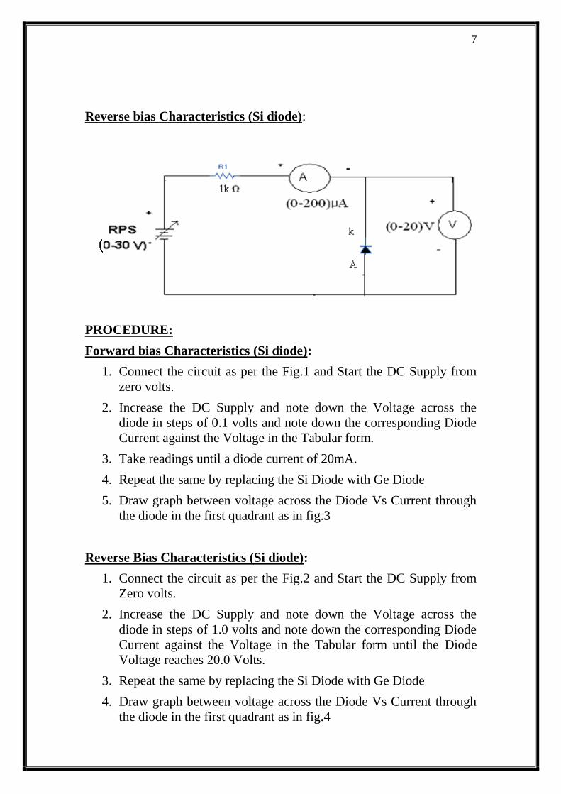
Reverse bias Characteristics (Si diode):
PROCEDURE:
Forward bias Characteristics (Si diode):
1. Connect the circuit as per the Fig.1 and Start the DC Supply from
zero volts.
2. Increase the DC Supply and note down the Voltage across the
diode in steps of 0.1 volts and note down the corresponding Diode
Current against the Voltage in the Tabular form.
3. Take readings until a diode current of 20mA.
4. Repeat the same by replacing the Si Diode with Ge Diode
5. Draw graph between voltage across the Diode Vs Current through
the diode in the first quadrant as in fig.3
Reverse Bias Characteristics (Si diode):
1. Connect the circuit as per the Fig.2 and Start the DC Supply from
Zero volts.
2. Increase the DC Supply and note down the Voltage across the
diode in steps of 1.0 volts and note down the corresponding Diode
Current against the Voltage in the Tabular form until the Diode
Voltage reaches 20.0 Volts.
3. Repeat the same by replacing the Si Diode with Ge Diode
4. Draw graph between voltage across the Diode Vs Current through
the diode in the first quadrant as in fig.4

8
TABULAR FORMS:
Forward Bias (Si diode):
Sl.no Voltmeter Reading Ammeter Reading
Reverse Bias (Si diode):
Sl.no Voltmeter Reading Ammeter Reading

9
MODEL GRAPH:
PRECAUTIONS:
1. Check the wires for continuity before use.
2. Keep the power supply at Zero volts before Start
3. All the contacts must be intact
RESULT:
Specifications Si diode
Cut in voltage
Break down voltage
Static Resistance F.Bias
R.Bias

10
Dynamic
Resistance
F.Bias
R.Bias
VIVA QUESTIONS:
1. Draw ideal Diode Volt Ampere Characteristics?
2. What is meant by cut in Voltage?
3. What are Static and Dynamic Resistances?
4. What is Diffusion Capacitance?
5. What are the specifications of a diode?
6. What is PIV?
7. Why leakage current is more for Ge Diode?
8. What is the current equation of the Diode?
9. What are the applications of PN junction diode?
10. What is the resistance of a diode in reverse bias condition?
11. Which direction does the conventional current in a PN junction
diode flows from?
12. What is other name for Zener diode?
13. Why do we use Zener diode as voltage regulator?
14. What are the difference between silicon and Zener diode?
15. What is meant by transition capacitance?
16. List out the difference between Zener and avalanche break down?
17. List out applications of Zener diode?
18. How does the doping concentration in Zener diode?
19. Does Zener diode have positive or negative temperature coefficient?
20. When does a Zener diode act as a regulator?

11
3. CHARATERSTICS OF DIODE:ZENER DIODE
AIM:
1. To obtain the forward Bias and Reverse Bias Characteristics of
Zener diode
2. To find the Cut-in Voltage & Breakdown Voltage
3. To find Static and Dynamic Resistance for forward and reverse
bias
4. Load Regulation Characteristics of Zener diode.
APPARATUS:
DC Regulated Power supply: (0–30) Volts
Diode : ECZ 5.1
Resistor :1K,560
D.C Ammeters : 0–20mA, 0–200A,0-200mA
D.C Volt meters :0–2V, 0-30V
Decade Resistance Box
Bread Board, connecting wires
CIRCUIT DIAGRAM:
Forward Bias Characteristics (Zener diode):

12
Reverse bias Characteristics (Zener diode):
Voltage Regulation (Zener diode):

13
PROCEDURE:
Forward bias Characteristics (Zener diode):
1. Connect the circuit as per the Fig. and Start the D.C.Supply from
Zero volts.
2. Increase the DC Supply and note down the Voltage across the
diode in steps of 0.1 volts and note down the corresponding Diode
Current against the Voltage in the Tabular form.
3. Draw graph between voltages across the Diode Vs Current through
the diode in the first quadrant as in fig.
Reverse Bias Characteristics (Zener diode):
1. Connect the circuit as per the Fig. and Start the D.C.Supply from
Zero volts.
2. Increase the DC Supply and note down the Voltage across the
diode in steps of 1 volts and note down the corresponding Diode
Current against the Voltage in the Tabular form.
3. Draw graph between voltage across the Diode Vs Current through
the diode in the Third quadrant as in fig.
Load Regulation Characteristics (Zener diode):
1. Connect the ckt as in Fig. and Keep the D.C Supply at a fixed
value (7.0V)
2. By changing the load Resistance take the readings of o/p Voltmeter
(Vo=Vz)
3. Now Keep the I/p Voltage at 10.0 V and 12.0 V and repeat the
above Procedure and Tabulate the observations

14
Zener Breakdown Voltage:
Draw a tangent on the reverse Bias Characteristic of the
Zener Diode starting from the Knee and touching most of the
points of the curve. The point where the tangent intersects the X-
axis is the Zener Breakdown Voltage.
TABLUAR FORM:
Forward Bias (Zener diode):
Sl.no Voltmeter Reading Ammeter Reading
Reverse Bias (Zener diode):

15
Sl.no Voltmeter Reading Ammeter Reading
MODEL GRAPH:
Zener
Diode Characteristics Load Regulation
Characteristics
16
PRECAUTIONS:
4. Check the wires for continuity before use.
5. Keep the power supply at Zero volts before Start
6. All the contacts must be intact
RESULT:
Specifications Zener diode
Cut in voltage
Break down voltage
Static Resistance F.Bias
R.Bias
Dynamic
Resistance
F.Bias
R.Bias
VIVA QUESTIONS:

17
1. Draw ideal Diode Volt Ampere Characteristics?
2. What is meant by cut in Voltage?
3. What are Static and Dynamic Resistances?
4. What is Diffusion Capacitance?
5. What are the specifications of a diode?
6. What is PIV?
7. Why leakage current is more for Ge Diode?
8. What is the current equation of the Diode?
9. What are the applications of PN junction diode?
10. What is the resistance of a diode in reverse bias condition
11. Which direction does the conventional current in a PN junction
diode flows from?
12. What is other name for Zener diode?
13. Why do we use Zener diode as voltage regulator?
14. What are the difference between silicon and Zener diode?
15. What is meant by transition capacitance?
16. List out the difference between Zener and avalanche break down?
17. List out applications of Zener diode?
18. How does the doping concentration in Zener diode?
19. Does Zener diode have positive or negative temperature coefficient?
20. When does a Zener diode act as a regulator?

18
4.. CHARATERSTICS OF LED
AIM:
To obtain the forward Bias and Reverse Bias Characteristics of Light
Emitting diode(LED)
APPARATUS:
DC Regulated Power supply: (0–30) Volts
Diode : LED
Resistor :1K
D.C Ammeters : 0–200A,0-200mA
D.C Volt meters :0–2V, 0-30V
Bread Board, connecting wires
CIRCUIT DIAGRAM:
Forward Bias Characteristics (LED):

19
Reverse bias Characteristics (LED):
PROCEDURE:
Forward bias Characteristics (LED):
1. Connect the circuit as per the Fig. and Start the D.C.Supply from
Zero volts.
2. Increase the DC Supply and note down the Voltage across the
diode in steps of 0.1 volts and note down the corresponding Diode
Current against the Voltage in the Tabular form.
20
3. Draw graph between voltages across the Diode Vs Current through
the diode in the first quadrant as in fig.
Reverse Bias Characteristics (LED):
1. Connect the circuit as per the Fig. and Start the D.C.Supply from
Zero volts.
2. Increase the DC Supply and note down the Voltage across the
diode in steps of 1 volts and note down the corresponding Diode
Current against the Voltage in the Tabular form.
3. Draw graph between voltage across the Diode Vs Current through
the diode in the Third quadrant as in fig.
TABLUAR FORM:
Forward Bias (LED):
Sl.no Voltmeter Reading Ammeter Reading

21
Reverse Bias (LED):
Sl.no Voltmeter Reading Ammeter Reading
MODEL GRAPH:
PRECAUTIONS:
22
1. Check the wires for continuity before use.
2. Keep the power supply at Zero volts before Start
3. All the contacts must be intact
RESULT:
VIVA QUESTIONS:
1. Draw ideal LED Volt Ampere Characteristics?
2. What is meant by cut in Voltage?
3. What are Static and Dynamic Resistances?
4. What are the specifications of LED?
5. What are the applications of LED?
6. What is the resistance of a LED in reverse bias condition?
7. Which direction does the conventional current in LED flows from?
8. What are the difference between silicon,Zener diode and LED?
9. How does the doping concentration in LED?
10. What is meant by Homojunction LED?
11. What is meant by Hetrojunction LED?
12. Differences between homojunction and hetrojunction LED.
13. What is meant by high radiance output?
14. What is meant by fast emission response?
15. what is meant by high quantum efficiency?
16. What is meant by Surface Emitter LED?
17. What is meant by Edge Emitter LED?
18. In LEDs light intensity depends on -----

23
19. Why GaAs used in fabrication of LEDs?
20. What is the type of emitted colour using GaAsP ?
6. DIODE AS A CIRCUIT ELEMENT: RECTIFIERS-HALF
WAVE RECTIFIERWITH RC FILTERS
AIM: To Conduct an experiment on Half Wave Rectifier with and
without capacitor Filter and to find out its Ripple factor and
percentage of Regulation.
APPARATUS:
1. Transformer : 230/9V
2. Diode :IN4001-1No
3. Capacitors :10f, 470f
4. Decade Resistance Box
5. Multimeter
6. Bread Board
CIRCUITDIAGRAM:
With Out Filter (Half wave):
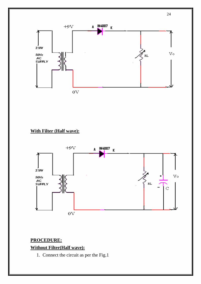
24
With Filter (Half wave):
PROCEDURE:
Without Filter(Half wave):
1. Connect the circuit as per the Fig.1

25
2. Keep the Load Resistance (DRB) at 100 ohms.
3. Apply A.C Signal and take the Vac and Vd.c Readings with the
help of Multimeter.
4. Repeat the above step by varying the load resistance in steps of 100
ohms.
5. Tabulate the readings.
6. Disconnect the DRB and note the Vd.cn (no Load)
7. Calculate ripple factor = Vac / Vd.c
8. Calculate Percentage of Regulation:
((V no load – V load) / Vno load) *100
With Capacitor Filter (Half wave):
1. Connect the circuit diagram as in fig 2 and repeat the method
followed in the earlier case and tabulate the readings.
2. Calculate the Ripple factor and Percentage of Regulation.
3. Calculate ripple factor = Vac / Vd.c
4. Calculate Percentage of Regulation:
((V no load – V load) / Vno load) *100
TABULAR FORM:
Without Filter (Half wave):
S.No
Load
Resistance
in ohms
O/P
Voltage
(Vo)
Vdc
Vac
Ripple
factor
% Of
Regulation
With Capacitor Filter (Half wave):

26
S.No
Load
Resistance
in ohms
O/P
Voltage
(Vo)
Vd.c
Va.c
Ripple
factor
% Of
Regulation
WAVE SHAPES (Half wave):

27
PRECAUTIONS:
1. Check the wires for continuity before use.
2. Keep the power supply at Zero volts before Start
3. All the contacts must be intact.
RESULT:
Without Filter:
Ripple Factor :
Regulation :
With Capacitor Filter:
Ripple Factor :
Regulation :
VIVAQUESTIONS:
1. How diode acts as a rectifier?
2. What is the significance of PIV? What is the condition imposed on
PIV?
3. What is meant by ripple factor? For a good filter whether ripple
factor should be high or low?
4. What is meant by regulation?
5. What happens to the o/p waveform if we increase the capacitor
value?
6. What happens if we increase the capacitor value?

28
7. Theoretical maximum efficiency of half wave rectifier is?
8. List out various parameters of half wave rectifier?
9. What is the use of capacitor in rectifier?
10. Define rectifier efficiency?
11. What is meant by TUF in rectifier?
12. What are the advantages of Bridge Rectifier over the center tapped
Rectifier?
13. What is the main advantage of a bridge rectifier compared to a full
wave rectifier is that?
14. List out various parameters in bridge rectifier?
15. What is formula for rectifier efficiency?
16. Derive efficiency expression for the bridge rectifier?
17. Derive the ripple factor expression for the bridge rectifier?
18. List the various components, which are used in your experiment?
19. Define Vdc, Idc, Vrms, and Irms?
20. What is the significance of the regulator?
7.PERFORMANCE OF FILTERS, FULL WAVE RECTIFIER
AIM: To Conduct Experiment on full wave rectifier center tapped circuit
with and without capacitor Filter and to find out its Ripple factor
and percentage of Regulation
APPARATUS:
1. Transformer : 230/9 V
2. Diodes : IN4001---2no.
3. Capacitors :10f, 470f.
4. Decade Resistance Box
5. Multimeter
6. Bread Board
CIRCIUTDIAGRAM:

29
With Out Filter:
With filter:

30
PROCEDURE:
Without Filter:
1. Connect the circuit as per the Fig.1
2. Keep the Load Resistance (DRB) at 100 ohms.
3. Apply A.C Signal and take the Vac and Vdc Readings with the
help of Millimeter.
4. Repeat the above step by varying the load resistance in steps of100
ohms
5. Tabulate the readings.
6. Disconnect the DRB and note the Vdc (no Load)
7. Calculate ripple factor = Vac / Vdc
8. Calculate Percentage of Regulation ((Vdc no load – Vdc load) /
Vdc no load) *100
With Capacitor Filter:
1. Connect the circuit diagram as in fig 2 and repeat the method
followed in the earlier case and tabulate the readings.
2. Calculate the Ripple factor and Percentage of Regulation.
3. Calculate ripple factor = Va.c / Vd.c
4. Calculate Percentage of Regulation
((Vdcno load – Vdc load) / Vdcno load) *100
TABULAR FORMS:
Without Filter:
S.No
Load
Resistance
in ohms
O/P
Voltage
(Vo)
Vdc
Vac
Ripple
factor
% Of
Regulation

31
With Capacitor Filter:
S.No
Load
Resistance
in ohms
O/P
Voltage
(Vo)
Vdc
Va.c
Ripple
factor
% Of
Regulation
WAVE SHAPES:

32
With Out Filter:
With filter:
PRECAUTIONS:
1. Check the wires for continuity before use.
2. Keep the power supply at Zero volts before Start
3. All the contacts must be intact
RESULT:
Without Filter:
Ripple Factor:
Regulation:
With Capacitor Filter:

33
Ripple Factor:
Regulation:
VIVA QUESTIONS:
1. What is a full wave rectifier?
2. How diode acts as a rectifier?
3. What is the significance of PIV requirement of diode in full wave
rectifier?
4. Compare capacitor filter with an inductor filter?
5. Draw the o/p waveform without filter? Draw the o/p? What is
waveform with filter?
6. What is meant by ripple factor? For a good filter whether ripple
factor should be high or low? What happens to the ripple factor if
we insert the filter?
7. What is meant by regulation? Why regulation is poor in the case of
inductor filter?
8. What is meant by time constant?

34
9. What happens to the o/p waveform if we increase the capacitor
value?
10. What happens if we increase the capacitor value?
11. What is the theoretical maximum value of ripple factor for a full
wave rectifier?
12. Draw the block diagram for power supply?
13. Why do we need filters in a power supply? Under what condition
we shall prefer a capacitor filter?
14. Define rectifier efficiency? What is the maximum theoretical
efficiency of full wave rectifier?
15. Full wave rectifier out put has a ripple factor of--?
16. List out the advantages of full wave rectifier?
17. Which direction the load current flows in full wave rectifier?
18. What is the significance of transformer in rectifier?
19. Compare half wave and full wave rectifiers from the point of view
of rectification efficiency?
20. What is the effect of turn’s ratio on full-wave rectifier output
voltage?
8.CHARATERISTICS OF PHOTODIODE
AIM: To obtain the characteristics of a photo diode and to find the dark
current.
APPARATUS:
1. DC regulated power supply : (0-30) V.
2. Photo diode TIL 84 : 1 no.
3. Resistor : 1K
4. DC ammeter : (0-500)A
5. DC voltmeter : (0-20) V
6. Breadboard :
7. Connecting wires :
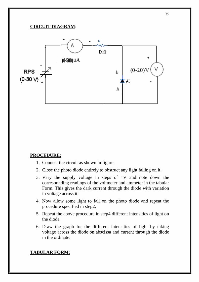
35
CIRCUIT DIAGRAM:
PROCEDURE:
1. Connect the circuit as shown in figure.
2. Close the photo diode entirely to obstruct any light falling on it.
3. Vary the supply voltage in steps of 1V and note down the
corresponding readings of the voltmeter and ammeter in the tabular
Form. This gives the dark current through the diode with variation
in voltage across it.
4. Now allow some light to fall on the photo diode and repeat the
procedure specified in step2.
5. Repeat the above procedure in step4 different intensities of light on
the diode.
6. Draw the graph for the different intensities of light by taking
voltage across the diode on abscissa and current through the diode
in the ordinate.
TABULAR FORM:

36
S.NO Intensity 0 Intensity 1 Intensity 2 Intensity 3
VR
(V)
IR
(mA)
VR
(V)
IR
(mA)
VR
(V)
IR
(mA)
VR
(V)
IR
(mA)
MODEL GRAPH:
PRECAUTIONS:
1. Check the wire for continuity before use.
2. Keep the power supply at zero volts before start.
3. All the connections must be intact.

37
RESULT:
Dark resistance of the photo diode is ----.
VIVA QUESTIONS:
1. Draw the schematic symbol of photo diode?
2. Explain the principle of photoconduction?
3. Define dark current?
4. What are the applications of photo diode?
5. In what sense does the photo diode differs from a rectifier diode?
6. An increase in the amount of light energy produces --------.
7. Photo diode can also be used as variable resistance.(true/false)
support your answer.
8. How much will be the dark current for this particular devise?
9. Photo diode is one of the fastest diode. (True/False).
10. In which region does the photo diode?
11. Draw the basic arrangement of biasing of a photodiode?
12. Why photo diode works in reverse bias condition only?
13. What are the materials used for the fabrication of diode ?
14. What is dark resistance in photo diode?
15. What are the Difference between photo diode and phototransistor?
16. Can we use the photo diode for AM generation?
17. Does photo diode works in forward bias condition?
18. Can we replace photo diode with ordinary diode?
19. Differentiate between Photo diode and LED?
20. What is the principle behind photoemission?

38
9.INPUT & OUTPUT CHARACTERISTICS OF BJT: CE
CONFIGURATIONS
AIM: To plot the input and output Characteristics of a transistor
connected in CE Configuration and to find the h – parameters from
the characteristics.
APPARATUS:
1. Dual Regulated D.C Power supply :(0–30) Volts
2. Transistor :BC107
3. Resistors: 1K, 120K
4. D.C, Ammeters :0-200A
5. Multimeter
CIRCUIT DIAGRAMS (CE configuration):

39
PROCEDURE (CE configuration):
1. Connect the circuit as per the Fig.
2. Keep VBB and VCC in zero volts before giving the supply
To find the input characteristics (CE configuration):
1. Keep VCE = 1 volt by varying VCC.
2. Vary VBB smoothly with fine control such that VBE varies in steps
of 0.1 volt from zero and note down the resulting base current IB
for each step in the tabular form.
3. Repeat the experiment for VCB =3.0 volts and 6.0 volts.
4. Draw a graph between VBE Vs IB against VCE = Constant.
To find the Output Characteristics (CE configuration):
1. Start VBB and VCC from zero Volts
2. Vary VBB such that IB = 50A, vary VCC such that VCE changes in
steps of 1.0 volt from zero up to 10 volts.

40
3. Note Down the resulting collector current IC for each step and
tabulate the readings.
4. Repeat the experiment for IB = 100A and IB = 200A and
IB=300A. Tabulate the readings.
To find the h – parameters (CE configuration):
Calculation of hre:
Draw a horizontal line at some constant IB value on the input
characteristics. Find VCE2,VCE1,VBE2,VBE1
VBE2 - VBE1
hrb = -----------------;
VCB2 - VCB1
Calculation of hie:
Mark two points on the input characteristics for constant VCE .let
the coordinates of these two points be (VBE1, IB1) and (VBE2,IB2).
VBE2 - VBE1
hie = ---------------- ;
IB2 - IB1
Calculation of hfe:
Draw a vertical line on the out put characteristics at some constant
VCE value. Find Ic2, Ic1 and IB2,IB1 .
,
IC2 - IC!
hfe = --------------- ;

41
IB2 - IB1
Calculation of hoe:
On the out put characteristics for a constant value of IB mark two
points with coordinates (VCE2 , IC2) and (VCE1 , IC1) .
IC2 - IC!
hoe = --------------- ;
VCE2 - VCE1
TABULAR FORM (CE configuration):
Input characteristics;
VCE OPEN VCE=1V VCE=2V VCE=3V VCE=6V
VBE
(VOLTS)
IB
(mA)
VBE
(VOLTS)
IB
(mA)
VBE
(VOLTS)
IB
(mA)
VBE
(VOLTS)
IB
(mA)
VBE
(VOLTS)
IB
(mA)
Output characteristics;

42
IB=50A IB=100A IB=200A IB=300A
VCE
(VOLTS)
IC
(mA)
VCE
(VOLTS)
IC
(mA)
VCE
(VOLTS)
IC
(mA)
VCE
(VOLTS)
IC
(mA)
MODEL GRAPHS:
Input characteristics: Output characteristics:
RESULT:
CE configuration: The input and out put characteristics are drawn on the
graphs and the h parameters are calculated.
hie= --------- ohms. hre= -----------
hoe= -------- mhos. hfe = -----------

43
VIVA QUESTIONS:
1. What is the need of characteristics of the transistor?
2. To draw the transistor characteristics, transistor must be kept in
which region of operation?
3. Mention the applications CB amplifier?
4. Mention the drawbacks of CB amplifier?
5. Why CB amplifier is useful in RF region?
6. In regulators what is the role of CB transistor mode of
operation?
7. What is the symbolic representation of the Current gain in CB
mode of operation?
8. Why early effect is much affected in the CB amplifier?
9. How do you maintain the operating point stable in case of a
transistor?
10. What is relation between , and ?
11. How much will be the input dynamic resistance in CE when we
compare with CB configuration?
12. How much will be the output dynamic resistance in CE
amplifier?
13. Out of three configurations which configuration has highest
leakage current?
14. How much will be the power gain in CE amplifier?
15. What is the advantage of cascaded amplifier?
16. For given emitter current collector current will be high if ------.
17. When determining the common emitter current gain by making
small changes in direct currents the collector voltage is held
constant so that the change in collector current is due to--------.
18. Which characteristics does determines the of a transistor?
19. What is the most noticeable effect of a small increase in
temperature in CE transistor configuration?
44
20. What are the disadvantages of cascade amplifier?
10. INPUT & OUTPUT CHARACTERISTICS OF BJT: CB
CONFIGURATIONS
AIM: To plot the input and output Characteristics of a transistor
connected in CB & CE Configuration and to find the h –
parameters from the characteristics.
APPARATUS:
6. Dual Regulated D.C Power supply :(0–30) Volts
7. Transistor :BC107
8. Resistors: 1K, 120K
9. D.C, Ammeters :0-500A---2no
10. Millimeter
CIRCUIT DIAGRAM (CB configuration):
45
PROCEDURE (CB configuration):
1. Connect the circuit as per the Fig.1
2. Keep VEE and VCC in zero volts before giving the supply
To find the input characteristics (CB configuration):
1 Keep VCB = 1 volt by varying VCC.
2 Vary VEE smoothly with fine control such that VEB varies in
steps of 0.1 volt from zero and note down the resulting emitter
current IE for each step in the tabular form.
3 Continue readings up to an emitter current of 450 A.
4 Repeat the experiment for VCB =3.0 volts and 6.0 volts.
5 Draw a graph between VEB Vs IE against VCB = Constant.
To find the Output Characteristics (CB configuration):

46
1 Start VEE and VCC from zero Volts
2 Vary VEE such that IE = 1mA, vary VCC such that VCB changes
in steps of 1.0 volts from zero up to 10 volts.
3 Note Down the resulting collector current IC for each step and
tabulate the readings.
4 Repeat the experiment for IE = 3mA and IE = 5mA and Ie=8mA.
Tabulate the readings.
To find the h – parameters (CB configuration):
Calculation of hrb:
Draw a horizontal line at some constant IE value on the input
characteristics. Find VCB2, VCB1, VEB2, VEB1
VEB2 - VEB1
hrb = -----------------;
VCB2 - VCB1
Calculation of hib:
Mark two points on the input characteristics for constant VCB .let
the coordinates of these two points be (VEB1, IE1) and (VEB2,IE2).
VEB2 - VEB1
hib = ---------------- ;
IE2 - IE1
Calculation of hfb:
Draw a vertical line on the out put characteristics at some constant
VCB value. Find Ic2, Ic1 and IE2, IE1.

47
IC2 - IC!
hfb = --------------- ;
IE2 - IE1
Calculation of hob:
On the out put characteristics for a constant value of IE mark two
points with coordinates (VCB2 , IC2) and (VCB1 , IC1) .
IC2 - IC!
hob = --------------- ;
VCB2 - VCB1
TABULAR FORMS (CB configuration):
Input characteristics;
VCB OPEN VCB=1V VCB=2V VCB=3V VCB=6V
VEB
(VOLTS)
IE
(mA)
VEB
(VOLTS)
IE
(mA)
VEB
(VOLTS)
IE
(mA)
VEB
(VOLTS)
IE
(mA)
VEB
(VOLTS)
IE
(mA)
Output characteristics;
IE=1mA IE=3mA IE=5mA IE=7mA

48
VCB
(VOLTS)
IC
(mA)
VCB
(VOLTS)
IC
(mA)
VCB
(VOLTS)
IC
(mA)
VCB
(VOLTS)
IC
(mA)
MODEL GRAPHS:
Input characteristics: Output characteristics:
CB configuration: The input and out put characteristics are drawn on the
graphs and the h parameters are calculated.
hib= --------- ohms. hrb= -----------
hob= -------- mhos. hfb = -----------
VIVA QUESTIONS:
1. What is the need of characteristics of the transistor?
2. To draw the transistor characteristics, transistor must be kept in
which region of operation?
3. Mention the applications CB amplifier?

49
4. Mention the drawbacks of CB amplifier?
5. Why CB amplifier is useful in RF region?
6. In regulators what is the role of CB transistor mode of
operation?
7. What is the symbolic representation of the Current gain in CB
mode of operation?
8. Why early effect is much affected in the CB amplifier?
9. How do you maintain the operating point stable in case of a
transistor?
10. What is relation between , and ?
11. How much will be the input dynamic resistance in CE when we
compare with CB configuration?
12. How much will be the output dynamic resistance in CE
amplifier?
13. Out of three configurations which configuration has highest
leakage current?
14. How much will be the power gain in CE amplifier?
15. What is the advantage of cascaded amplifier?
16. For given emitter current collector current will be high if ------.
17. When determining the common emitter current gain by making
small changes in direct currents the collector voltage is held
constant so that the change in collector current is due to--------.
18. Which characteristics does determines the of a transistor?
19. What is the most noticeable effect of a small increase in
temperature in CE transistor configuration?
20. What are the disadvantages of cascade amplifier?

50
11. DRAIN & TRANSFER CHARECTERISTICS OF JFET
AIM: To conduct an experiment on a given JFET and obtain
(1) Drain Characteristics,
(2) Transfer Characteristics,
(3) From the characteristics find rd, gm, and .
APPARATUS:
1. Dual Regulated D.C Power supply: (0–30) V
2. JFET : BFW10 or 11
3. D.C Ammeters :0–25mA
4. Millimeter

51
CIRCUIT DIAGRAMS:
PROCEDURE:
Drain Characteristics:
1. Connect the circuit as per the Fig.1 and Start with VGG and VDD
keeping at Zero volts.
2. Keep Vgg such that VGS=0 volts Now Vary VDD such that VDS
Varies in steps of 1 Volt up to 10 Volts. And Note down the
corresponding Drain Current Id. and Tabulate.
3. Repeat the above Experiment with VGS = -1 V and –2V and
tabulate the readings.
4. Draw a graph VDS Vs ID against VGS as parameters on graph.
5. From the above graph calculate rd down the corresponding Diode
Current against the Voltage in the Tabular form.
6. Draw graph between voltage across the Diode Vs Current through
the diode in the first quadrant as in fig

52
Transfer Characteristics:
1. Set VGG and VDD at Zero Volts. Keep VDS = 1 Volt.
2. Vary VGG Such That VGS Varies in steps of 0.5 Volts. Note down
the corresponding Drain Current ID. and Tabulate the readings.
3. Repeat the above experiment for VDS=3.0 V and 5.0 V and tabulate
the readings.
4. Draw graph VGS Vs ID with VDS as parameter.
5. From the Graph Find gm .
6. Now = gm rd.
TABULAR FORMS:
Drain Characteristics:
S.No VDS (Volts) VGS= 0 V VGS= -1 V VGS=-2 V
ID (mA) ID (mA) ID (mA)
Transfer Characteristics:
S.No VGS (Volts) VDS= 1.0 V VDS= 3.0
V
VDS=5.0 V

53
ID (mA) ID (mA) ID (mA)
MODEL GRAPHS:
Drain Characteristics: Transfer Characteristics:
CALCULATIONS:
Calculation of rd:
Construct a Triangle on one of the O/p Characteristic for a
particular VGS in the active region and Find VDS and ID
Now rd = VDS /ID (VGS =Constant)
Calculation of gm:
Construct a Triangle on one of the transfer characteristics for a
particular VDS find VGS and ID
Now gm = ID/ VGS (VDS = Constant)

54
Calculation of :
= gm rd.
PRECAUTIONS:
1. Check the wires for continuity before use.
2. Keep the power supply at Zero volts before Start
3. All the contacts must be intact
4. For a good JFET ID will be 11.0 mA at VGS = 0.0 Volts if not
change the JFET.
RESULTS:
Drain Resistance Now rd. = Ohms.
Tran Conductance gm = mhos
Amplification Factor =
VIVA QUESTIONS:
1. What are the advantages of JFET over BJT?
2. Why input resistance in FET amplifier is more than BJT amplifier
3. What is a Uni polar Device?
4. What is Pinch off Voltage?
5. What are the various FETs?
6. What is Enhancement mode and depletion mode?
7. Draw the equivalent circuit of JFET for Low frequencies
8. Write the mathematical equation for gm in terms of gmo.
9. Write equation of FET ID in terms of VGS and VP.
10. What is the effect of Gate to source voltage on Drain
characteristics?
11. On what carriers do the FET operates?

55
12. If the J-FET is operating above pinch off voltage, what happens to
the drain current?
13. Why JFET is also called square law device?
14. What is the difference between FET and BJT?
15. What is meant by trans conductance?
16. What is meant by Breakdown region?
17. What happens to the drain current in the curve AB region?
18. Transfer characteristics are also called.
19. What is meant by application factor?
20. What are the types of JFET?
12. EMITTER FOLLOWER CHARACTERISTIC & AMPLIFIER
AIM: To find the frequency response of a Emitter follower Transistor
Amplifier and to fine the bandwidth from the response, voltage
gain, input resistance.
APPARATUS:
Dual regulated DC power supply : (0-30) V
Transistor : BC 107
Resistors :100K, 10K, 3.3K, 4.7K,
1K
Capacitors :50f, 10 f-3no
Potentiometer :
CRO :
56
Signal generator : (0-1MHz)
Test board
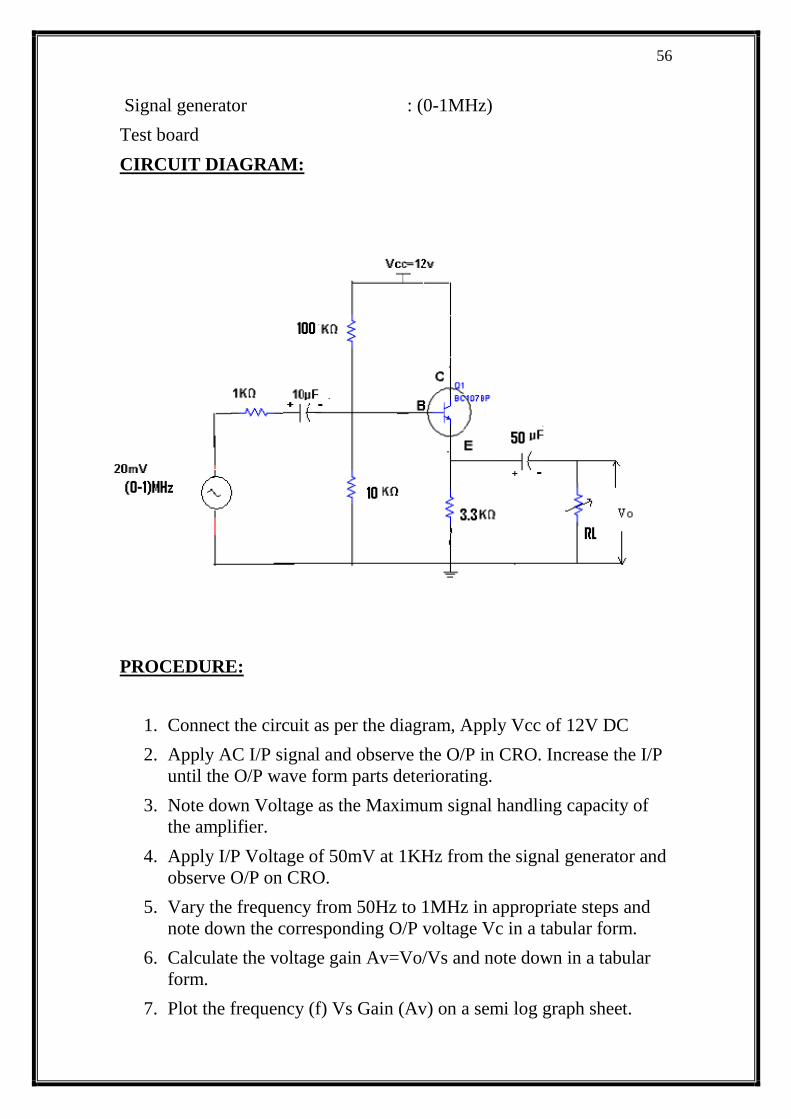
CIRCUIT DIAGRAM:
PROCEDURE:
1. Connect the circuit as per the diagram, Apply Vcc of 12V DC
2. Apply AC I/P signal and observe the O/P in CRO. Increase the I/P
until the O/P wave form parts deteriorating.
3. Note down Voltage as the Maximum signal handling capacity of
the amplifier.
4. Apply I/P Voltage of 50mV at 1KHz from the signal generator and
observe O/P on CRO.
5. Vary the frequency from 50Hz to 1MHz in appropriate steps and
note down the corresponding O/P voltage Vc in a tabular form.
6. Calculate the voltage gain Av=Vo/Vs and note down in a tabular
form.
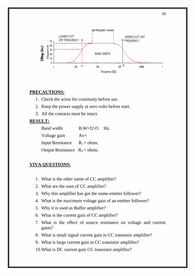
7. Plot the frequency (f) Vs Gain (Av) on a semi log graph sheet.
57
8. Draw a horizontal line at 0.707times Av and note down the cut off
points and the bandwidth is given by B.W=f2-f1.
INPUT RESISTANCE Ri:
1. Apply input voltage of 50mV at 1KHz from the signal generator
and observe the O/P on CRO.
2. With out Disturbing the set up note Vi
3. Find Ii=(Vs-Vi)/Rs and Ri=Vi/Ii.
OUTPUT RESISTANCE Ro:
1. Apply I/P Voltage of 50mV at 1KHz from the signal generator and
observe the O/P on CRO.
2. Connect a Potentiometer across the O/P terminals and without
disturbing Vs, adjust the potentiometer such that O/P falls to Vo/2.
3. The resistance of the potentiometer is equal to R0. .
TABULAR FORMS:
S.NO Frequency
(f)
O/P voltage
(V0)
Voltage gain
Av=V0/Vi
Av in
dB=20log(V0/Vi)
MODEL GRAPH:
58
PRECAUTIONS:
1. Check the wires for continuity before use.
2. Keep the power supply at zero volts before start.
3. All the contacts must be intact.
RESULT:
Band width B.W=f2-f1 Hz.
Voltage gain Av=
Input Resistance Ri = ohms.
Output Resistance R0 = ohms.
VIVA QUESTIONS:
1. What is the other name of CC amplifier?
2. What are the uses of CC amplifier?
3. Why this amplifier has got the name emitter follower?
4. What is the maximum voltage gain of an emitter follower?
5. Why it is used as Buffer amplifier?
6. What is the current gain of CC amplifier?
7. What is the effect of source resistance on voltage and current
gains?
8. What is small signal current gain in CC transistor amplifier?
9. What is large current gain in CC transistor amplifier?
10. What is DC current gain CC transistor amplifier?

59
11. What is the o/p impedance of the CC amplifier?
12. What is the roll of CC amplifier in bootstrap Darlington pair?
Is there any constant current region in the CC amplifier?
13. What is meant by impedance matching?
14. Why CC amplifier is used as a impendence matching device?
15. How bandwidth is affected in CC amplifier (high or low)?
16. What is meant by early effect?
17. What is meant by maximum power dissipation?
18. When does the transistor is said to be in saturation region?
19. What is meant by thermal run away?
20. What is the advantage of CC amplifier?
13. SWITCHING CHARACTERISTICS OF BJT
AIM:
1. To observe the action of a transistor as an electronic switch.
2. To measure the voltage across the transistor when it is ON and
when it is OFF.
APPARATUS:
Regulated power supply :(0-30) V.
Transistor : BC 107.
Resistors : 4.7K--2 no, 2.2K
Multimeter :
LED. :
CIRCUIT DIAGRAM:

60
PROCEDURE:
1. Connect the circuit as shown in figure.
2. Give 0V as input and measure voltage across Collector to
Emitter (VCE), Collector to Base (VCB).
3. Give 5V as input and measure voltage across Collector to
Emitter (VCE), Collector to Base (VCB).
4. Observe the state of LED at steps 2 and 3.
5. Tabulate the readings.
TABULAR FORM:
INPUT
VOLTAGE
VCE VCB VBE Transistor
mode
ON/OFF
MODE
OF LED
61
0 VOLTS
5 VOLTS
RESULT: The action of transistor as an electronic switch is observed
and voltage is measured across the transistor terminal, when
it is ON and when it is OFF.
VIVA QUESTIONS:
1. Define ON/OFF time?
2. In which region transistor acts as an open switch?
3. In which region transistor will be in ON region?
4. What do you mean by saturation region?
5. What do you mean by cut off region?
6. What do you mean by active region?
7. What are the advantages of electronic switch over mechanical
switch?
8. When a transistor is said to be in a quiescent state?
9. One way in which the operation of an NPN transistor differs from
that of a PNP transistor is that?
10. What do you mean by emitter, base and collector of a transistor?
11. What happens, if the both emitter and collectors are reverse biased
in case of a transistor?
12. How a transistor is connected in a circuit?

62
13. How can a transistor be used as a switch?
14. What are the advantages of a BJT?
15. Explain the function of emitter in the operation of a junction
transistor? What do you understand by the collector reverse
saturation current?
16. In which configuration (CB or CE) does it have a greater value?
17. The arrowhead on the transistor symbol always points in the
direction of?
18. What are the different configurations in transistor?
19. Compared to a CB amplifier, the CE amplifier has?
20. The main current crossing the collector junction in a normally
biased NPN is?
14. MEASUREMENT OF h-PARAMETERS, TRANSISTOR AS AN
AMPLIFIER
AIM: To find the frequency response of a Common Emitter Transistor
Amplifier and to find the Bandwidth from the Response, Voltage
gain, Input Resistance, output resistance
APPARATUS:
Dual Regulated D.C Power supply: (0–30) V
Transistor : BC107
Resistors :100k, 10K,1K-2 no.,4.7K.
Capacitors :50f-2no., 10f.
Potentiometer :
CRO :
Signal Generator : (0 – 1MHz)
Bread Board :

63
CIRCUIT DIAGRAM:
PROCEDURE:
1. Connect the circuit as per the Fig.1.Apply Vcc of 12 Volts D.C.
2. Apply I/p Voltage of 20mV at 1KHz from the Signal Generator
and observe the o/p on CRO.
3. Vary the frequency from 50 Hz to 600KHz in appropriate steps and
note down the corresponding o/p Voltage Vo in a tabular Form.
4. Calculate the Voltage Gain Av = Vo/Vs and note down in the
tabular form.
5. Plot the frequency (f) Vs Gain (Av) on a semi log Graph sheet
6. Draw a horizontal line at 0.707 times Av and note down the cut off
points and the Bandwidth is given by B.W = f2 – f1.
Input Resistance Ri:

64
1. Apply I/p Voltage of 20mV at 1KHz from the Signal Generator
and observe the o/p on CRO
2. Without disturbing the setup note Vi
3. Find Ii = (Vs – Vi) / Rs and Ri= Vi / Ii Ohms.
Output Resistance Ro:
1. Apply I/p Voltage of 50mV at 1KHz from the Signal Generator
and observe the o/p on CRO
2. Connect a Potentiometer across the o/p terminals and without
disturbing Vs adjust the potentiometer such that o/p falls to V0/2
3. The Resistance of the potentiometer is equal to Ro.
TABULAR FORMS:
I/p Voltage Vs = 20mV
S.No Frequency
(f)
O/P Voltage
(Vo)
Voltage Gain Av
=Vo/Vi
Av in dB=
20 log (Vo/Vi)
MODEL GRAPH:

65
PRECAUTIONS:
1. Check the wires for continuity before use.
2. Keep the power supply at Zero volts before Start
3. All the contacts must be intact
RESULT:
Bandwidth B.W = f2 – f1 = Hz
Voltage Gain Av =
Input Resistance Ri = ohms
Output Resistance Ro = ohms
VIVA QUESTIONS:
1. What is the need of characteristics of the transistor?
2. What are the characteristics required for drawing the Q-point?
3. To draw the transistor characteristics, transistor must be kept in
which region of operation?
4. By the CE characteristics the impedance parameters are ----.
5. By the CE characteristics gain parameters are -----.
6. Mention the applications CE amplifier?
7. Mention the drawbacks of CE amplifier?
8. What are the typical h-parameter values for CE amplifier?
9. Why CE amplifier is widely used in amplifier circuits?
10. What is the difference between active and passive components?

66
11. What is the significance of drawing the load line??
12. Current gain of the CE amplifier is represented as----.
13. How much will be the voltage gain in CE amplifier?
14. What are the input characteristics of CE transistor?
15. What are the output characteristics of CE transistor?
16. How do you maintain the operating point stable in case of a
transistor?
17. In which region transistor can act as a switch?
18. What is relation between , and ?
19. How a transistor is connected in a circuit?
20. What do you mean by bipolar transistor?
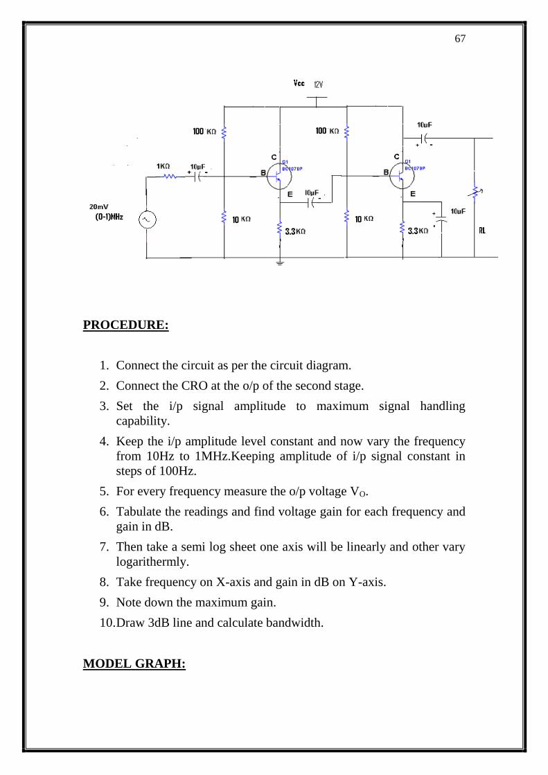
15. FREQUENCY RESPONSE OF (CC-CE) TWO-STAGE
TRANSISTOR AMPLIFIER
AIM: To plot the frequency response of the two stage (CC-CE) amplifier
and find the bandwidth
APPARATUS:
1. Transistor : BC107-2no
2. Resistors : 100K –2no, 3.3K –2no, 10K –2no, 4.7K ,
1K.
3. Capacitors : 10F-4 no
CIRCUIT DIAGRAM:
67
PROCEDURE:
1. Connect the circuit as per the circuit diagram.
2. Connect the CRO at the o/p of the second stage.
3. Set the i/p signal amplitude to maximum signal handling
capability.
4. Keep the i/p amplitude level constant and now vary the frequency
from 10Hz to 1MHz.Keeping amplitude of i/p signal constant in
steps of 100Hz.
5. For every frequency measure the o/p voltage VO.
6. Tabulate the readings and find voltage gain for each frequency and
gain in dB.
7. Then take a semi log sheet one axis will be linearly and other vary
logarithermly.
8. Take frequency on X-axis and gain in dB on Y-axis.
9. Note down the maximum gain.
10. Draw 3dB line and calculate bandwidth.
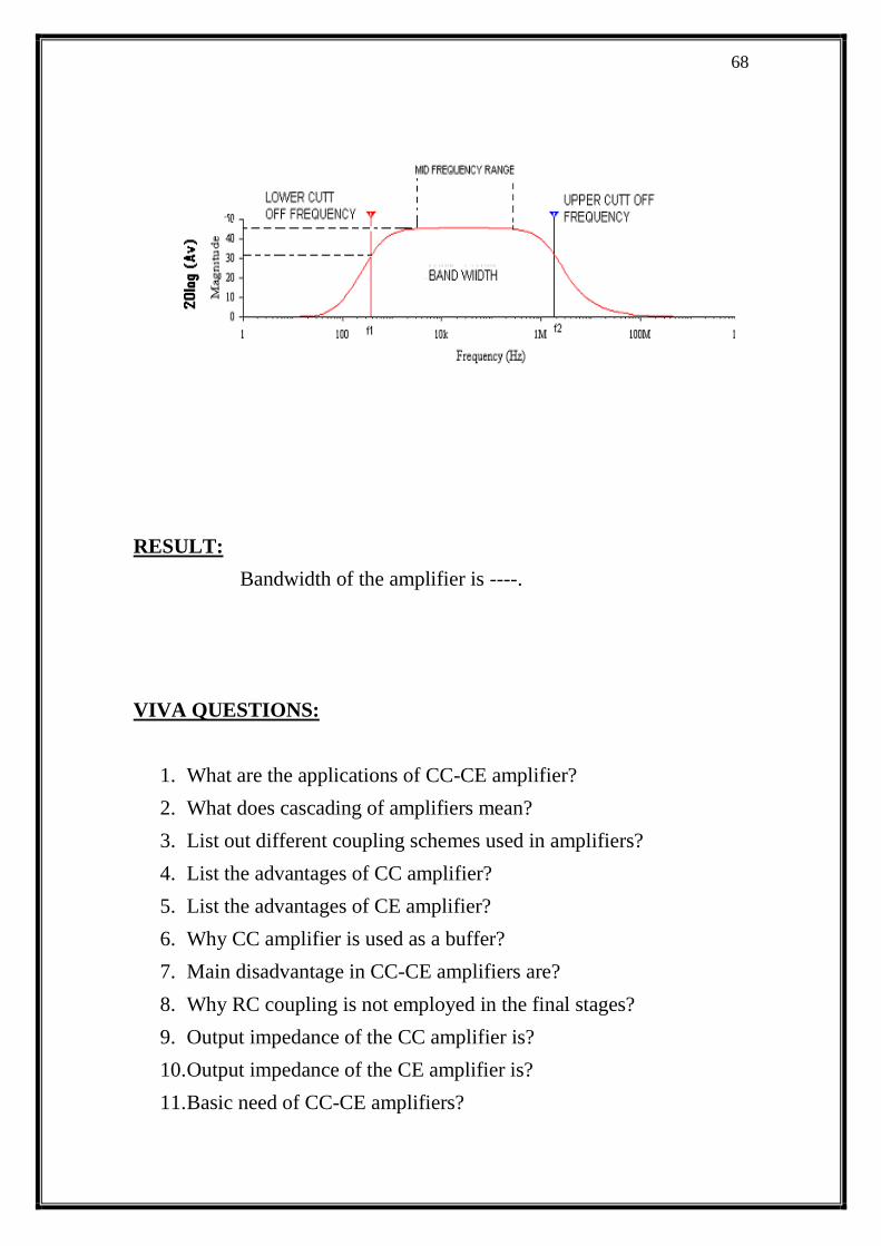
MODEL GRAPH:
68
RESULT:
Bandwidth of the amplifier is ----.
VIVA QUESTIONS:
1. What are the applications of CC-CE amplifier?
2. What does cascading of amplifiers mean?
3. List out different coupling schemes used in amplifiers?
4. List the advantages of CC amplifier?
5. List the advantages of CE amplifier?
6. Why CC amplifier is used as a buffer?
7. Main disadvantage in CC-CE amplifiers are?
8. Why RC coupling is not employed in the final stages?
9. Output impedance of the CC amplifier is?
10. Output impedance of the CE amplifier is?
11. Basic need of CC-CE amplifiers?

69
12. How the gain bandwidth product effects in CC-CE amplifier?
13. List out difference between cascade and cascode amplifiers?
14. List out the advantages of Darlington pair amplifier?
15. Define Bandwidth?
16. What does bootstrap amplifier mean?
17. Two stage of multistage amplifier have a gain of 50 and 20.The dB
voltage gain is?
18. Differential amplifier, cascode amplifier, cascade amplifier, among
these, which is having highest ft?
19. Gain bandwidth product is always constant for any amplifier circuit
says True or False? Explain briefly?
20. What is the approximate current gain in Darlington pair?
16. BIAS STABILISATION
AIM: The addition of the emitter resistor to the DC bias of BJT provides
improved stability.
To calculate the stability factor(s) for both fixed bias and self-bias
APPARATUS:
1. Regulated Power supply:(0–30) V
2. Transistor : BC107
3. Resistors : Rs, Re, R1, R2, and Rc as per Design
4. Capacitors : 50f---2no., 10f ----1 no.
5. CRO
6. Signal Generator : (0 – 1MHz)

70
7. Bread Board
CIRCUIT DIAGRAM:
Selfbias Circuit:
DESIGN PROCEDURE:
Icq = 5mA, Vceq = 6.0 V, Vcc = 12.0 V, Rc = 1K, S = 25,Vbe=0.6 V.
Find hfe of the transistor
S= (1+) / (1+Re / (Re + Rb)
VB = VCCR2 / (R1 +R2)
RB = R1R2 / (R1+R2)
VB = IBRB+ VBE + (1+) IB RE
VCC = ICRC +VCE+(1+) IB RE
Using the above formula find Re, R1, R2.
Stability factor can be calculated as follows:
FIXED BIAS:
IB=VRB/RB mA.
IC=VRC/RC mA.

71
=IC/IB. And S=1+.
VCE = VCC- IC RC
SELF-BIAS:
I1 =VR!/R1 mA.
I2=VR2/R2 mA.
IE=VRE/RE mA.
IB=I1-I2 mA.
IC=-IE+IB mA and. =IC/IB.
S=(1+.)(1+RB/RE)/(1++RB/RE).
Where RB=R1R2/(R1+R2).
EMITTER STABILIZAED BIAS:
IB = (VCC - VBE)/ (RB+(+1) RE)
IC = IB
VCE = VCC- IC (RC+ RE)
PROCEDURE:
1. Connect the circuit as per the figure
2. Apply Vcc of 12 Volts D.C.
3. Using the Multimeter find the voltage drop across RB and RC.
4. Using these voltages find IB and IC.
5. Calculate the value using IB and IC.
6. Calculate the stability factor S using the above formulae.
7. Repeat the same procedure for self-bias, Emitter stabilized bias.
8. Prepare the table for fixed and emitter bias circuits.

72
TABULAR FORM:
IB (A) IC (mA) VCE (V)
PRECAUTIONS:
1. Check the wires for continuity before use.
2. Keep the power supply at Zero volts before Start
3. All the contacts must be intact
RESULT: Stability is improved by adding emitter resistor to the fixed
bias circuit.
The stability factor for fixed bias=----.
The stability factor for self-bias=----.
VIVA QUESTIONS:
1. What is meant by Self Bias and fixed bias circuits, which one is
preferred and why?
2. What is the significance of Emitter Resistance?
3. What is stability factor?
4. What is DC load line and AC load line?
5. What is quiescent point? What are the various parameters of the
transistor that cause drift in q-point?
6. What are different techniques of stabilization?
7. Relate stability factor with the circuit parameters
8. What is the relation between and ?

73
9. If bypass capacitor is removed, what happens to the gain?
10. What is meant by base bias? What is its disadvantage?
11. What is meant by Q-point?
12. What is the need of biasing?
13. What is advantage of fixed bias over self-bias?
14. List out the methods of transistor biasing?
15. What are the different conditions for biasing the transistor?
16. What are the factors that are affecting stability of Q-point?
17. What is the other name for self-bias?
18. What is the other name for fixed bias?
19. What is the need of heat sinkers in the biasing circuits?
20. Explain the concept of thermal run away in the biasing circuits?