single/dual/quad, micropower, single-supply, rail-to-rail ... · pdf fileaccuracy with...
TRANSCRIPT

General DescriptionThe single MAX4091, dual MAX4092, and quadMAX4094 operational amplifiers combine excellent DCaccuracy with Rail-to-Rail® operation at the input andoutput. Since the common-mode voltage extends fromVCC to VEE, the devices can operate from either a sin-gle supply (2.7V to 6V) or split supplies (±1.35V to±3V). Each op amp requires less than 130µA of supplycurrent. Even with this low current, the op amps arecapable of driving a 1kΩ load, and the input-referredvoltage noise is only 12nV/√Hz. In addition, these opamps can drive loads in excess of 2000pF.
The precision performance of the MAX4091/MAX4092/MAX4094 combined with their wide input and outputdynamic range, low-voltage, single-supply operation,and very low supply current, make them an idealchoice for battery-operated equipment, industrial, anddata acquisition and control applications. In addition,the MAX4091 is available in space-saving 5-pin SOT23,8-pin µMAX, and 8-pin SO packages. The MAX4092 isavailable in 8-pin µMAX and SO packages, and theMAX4094 is available in 14-pin TSSOP and 14-pin SOpackages.
________________________ApplicationsPortable Equipment
Battery-Powered Instruments
Data Acquisition and Control
Low-Voltage Signal Conditioning
Features Low-Voltage, Single-Supply Operation (2.7V to 6V)
Beyond-the-Rails™ Inputs
No Phase Reversal for Overdriven Inputs
30µV Offset Voltage
Rail-to-Rail Output Swing with 1kΩ Load
Unity-Gain Stable with 2000pF Load
165µA (max) Quiescent Current Per Op Amp
500kHz Gain-Bandwidth Product
High Voltage Gain (115dB)
High Common-Mode Rejection Ratio (90dB) andPower-Supply Rejection Ratio (100dB)
Temperature Range (-40°C to +125°C)
MA
X4
09
1/M
AX
40
92
/MA
X4
09
4
Single/Dual/Quad, Micropower, Single-Supply,Rail-to-Rail Op Amps
________________________________________________________________ Maxim Integrated Products 1
VCC1OUT 1
2
3
4
8
7
6
5
VCC
OUT2
IN2-
IN2+VEE
IN1+
IN1-
OUT1
µMAX/SO
TOP VIEW
1
2
3
4
8
7
6
5
N.C.
VCC
OUT
N.C.VEE
IN+
IN-
N.C.
µMAX/SO
5
4 IN-3IN+
2VEE
SOT23
14
13
12
11
10
9
8
1
2
3
4
5
6
7
OUT4
IN4-
IN4+
VEEVCC
IN1+
IN1-
OUT1
IN3+
IN3-
OUT3OUT2
IN2-
IN2+
TSSOP/SO
4
MAX4091MAX4091 MAX4092
MAX4094
Pin Configurations/Functional Diagrams
19-2272; Rev 0; 1/02
For pricing, delivery, and ordering information, please contact Maxim/Dallas Direct! at 1-888-629-4642, or visit Maxim’s website at www.maxim-ic.com.
Ordering Information
PART TEMP RANGE PIN-PACKAGE
MAX4091AUK-T -40°C to +125°C 5 SOT23-5
MAX4091ASA -40°C to +125°C 8 SO
MAX4091AUA -40°C to +125°C 8 µMAX
MAX4092ASA -40°C to +125°C 8 SO
MAX4092AUA -40°C to +125°C 8 µMAX
MAX4094AUD -40°C to +125°C 14 TSSOP
MAX4094ASD -40°C to +125°C 14 SO
Rail-to-Rail is a registered trademark of Nippon Motorola, Ltd.Beyond-the-Rails is a trademark of Maxim Integrated Products, Inc.
MA
X4
09
1/M
AX
40
92
/MA
X4
09
4
Single/Dual/Quad, Micropower, Single-Supply,Rail-to-Rail Op Amps
2 _______________________________________________________________________________________
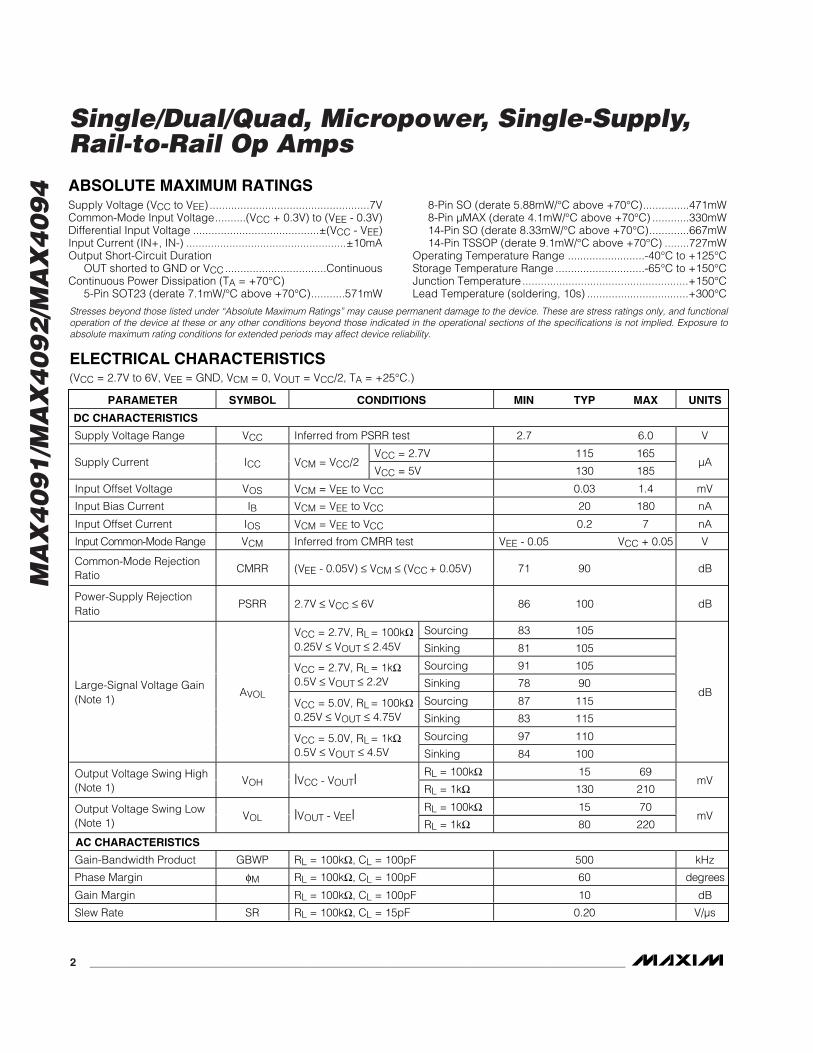
ABSOLUTE MAXIMUM RATINGS
ELECTRICAL CHARACTERISTICS(VCC = 2.7V to 6V, VEE = GND, VCM = 0, VOUT = VCC/2, TA = +25°C.)
Stresses beyond those listed under “Absolute Maximum Ratings” may cause permanent damage to the device. These are stress ratings only, and functionaloperation of the device at these or any other conditions beyond those indicated in the operational sections of the specifications is not implied. Exposure toabsolute maximum rating conditions for extended periods may affect device reliability.
Supply Voltage (VCC to VEE) ....................................................7VCommon-Mode Input Voltage..........(VCC + 0.3V) to (VEE - 0.3V)Differential Input Voltage .........................................±(VCC - VEE)Input Current (IN+, IN-) ....................................................±10mAOutput Short-Circuit Duration
OUT shorted to GND or VCC.................................ContinuousContinuous Power Dissipation (TA = +70°C)
5-Pin SOT23 (derate 7.1mW/°C above +70°C)...........571mW
8-Pin SO (derate 5.88mW/°C above +70°C)...............471mW8-Pin µMAX (derate 4.1mW/°C above +70°C) ............330mW14-Pin SO (derate 8.33mW/°C above +70°C).............667mW14-Pin TSSOP (derate 9.1mW/°C above +70°C) ........727mW
Operating Temperature Range .........................-40°C to +125°CStorage Temperature Range .............................-65°C to +150°CJunction Temperature ......................................................+150°CLead Temperature (soldering, 10s) .................................+300°C
PARAMETER SYMBOL CONDITIONS MIN TYP MAX UNITS
DC CHARACTERISTICS
Supply Voltage Range VCC Inferred from PSRR test 2.7 6.0 V
VCC = 2.7V 115 165Supply Current ICC VCM = VCC/2
VCC = 5V 130 185µA
Input Offset Voltage VOS VCM = VEE to VCC 0.03 1.4 mV
Input Bias Current IB VCM = VEE to VCC 20 180 nA
Input Offset Current IOS VCM = VEE to VCC 0.2 7 nA
Inp ut C om m on- M od e Rang e VCM Inferred from CMRR test VEE - 0.05 VCC + 0.05 V
Common-Mode RejectionRatio
CMRR (VEE - 0.05V) ≤ VCM ≤ (VCC + 0.05V) 71 90 dB
Power-Supply RejectionRatio
PSRR 2.7V ≤ VCC ≤ 6V 86 100 dB
Sourcing 83 105VCC = 2.7V, RL = 100kΩ0.25V ≤ VOUT ≤ 2.45V Sinking 81 105
Sourcing 91 105VCC = 2.7V, RL = 1kΩ0.5V ≤ VOUT ≤ 2.2V Sinking 78 90
Sourcing 87 115VCC = 5.0V, RL = 100kΩ0.25V ≤ VOUT ≤ 4.75V Sinking 83 115
Sourcing 97 110
Large-Signal Voltage Gain(Note 1)
AVOL
VCC = 5.0V, RL = 1kΩ0.5V ≤ VOUT ≤ 4.5V Sinking 84 100
dB
RL = 100kΩ 15 69Output Voltage Swing High(Note 1)
VOH |VCC - VOUT|RL = 1kΩ 130 210
mV
RL = 100kΩ 15 70Output Voltage Swing Low(Note 1)
VOL |VOUT - VEE|RL = 1kΩ 80 220
mV
AC CHARACTERISTICS
Gain-Bandwidth Product GBWP RL = 100kΩ, CL = 100pF 500 kHz
Phase Margin φM RL = 100kΩ, CL = 100pF 60 d eg r ees
Gain Margin RL = 100kΩ, CL = 100pF 10 dB
Slew Rate SR RL = 100kΩ, CL = 15pF 0.20 V/µs

MA
X4
09
1/M
AX
40
92
/MA
X4
09
4
Single/Dual/Quad, Micropower, Single-Supply,Rail-to-Rail Op Amps
_______________________________________________________________________________________ 3
ELECTRICAL CHARACTERISTICS (continued)(VCC = 2.7V to 6V, VEE = GND, VCM = 0, VOUT = VCC/2, TA = +25°C.)
PARAMETER SYMBOL CONDITIONS MIN TYP MAX UNITS
Input-Noise Voltage Density eN f = 10kHz 12 nV/√HzInput-Noise Current Density f = 10kHz 1.5 pA/√Hz
Noise Voltage(0.1Hz to 10Hz)
16 µVRMS
Total Harmonic DistortionPlus Noise
THD + Nf = 1kHz, RL = 10kΩ, CL = 15pF,AV = 1, VOUT = 2VP-P
0.003 %
Capacitive-Load Stability CLOAD AV = 1 2000 pF
Settling Time tS To 0.1%, 2V step 12 µs
Power-On Time tONVCC = 0 to 3V step, VIN = VCC/2,AV = 1
2 µs
Op-Amp Isolation f = 1kHz (MAX4092/MAX4094) 125 dB
ELECTRICAL CHARACTERISTICS(VCC = 2.7V to 6V, VEE = GND, VCM = 0, VOUT = VCC/2, TA = TMIN to TMAX, unless otherwise noted. Typical values specified at TA = +25°C.) (Note 2)
PARAMETER SYMBOL CONDITIONS MIN TYP MAX UNITS
DC CHARACTERISTICS
Supply Voltage Range VCC Inferred from PSRR test 2.7 6.0 V
VCC = 2.7V 200Supply Current ICC VCM = VCC/2
VCC = 5V 225µA
Input Offset Voltage VOS VCM = VEE to VCC ±3.5 mV
Input Offset Voltage Tempco ∆VOS/∆T ±2 µV/°C
Input Bias Current IB VCM = VEE to VCC ±200 nA
Input Offset Current IOS VCM = VEE to VCC ±20 nA
Input Common-Mode Range VCM Inferred from CMRR test V E E - 0.05 V C C + 0.05 V
Common-Mode Rejection Ratio CMRR (VEE - 0.05V) ≤ VCM ≤ (VCC + 0.05V) 62 dB
Power-Supply Rejection Ratio PSRR 2.7V ≤ VCC ≤ 6V 80 dB
Sourcing 82VCC = 2.7V, RL = 100kΩ0.25V ≤ VOUT ≤ 2.45V Sinking 80
Sourcing 90VCC = 2.7V, RL = 1kΩ0.5V ≤ VOUT ≤ 2.2V Sinking 76
Sourcing 86VCC = 5V, RL = 100kΩ0.25V ≤ VOUT ≤ 4.75V Sinking 82
Sourcing 94
Large-Signal Voltage Gain(Note 1)
AVOL
VCC = 5V, RL = 1kΩ0.5V ≤ VOUT ≤ 4.5V Sinking 80
dB
RL = 100kΩ 75Output Voltage Swing High(Note 1)
VOH VCC - VOUTRL = 1kΩ 250
mV
RL = 100kΩ 75Output Voltage Swing Low(Note 1)
VOL VOUT - VEERL = 1kΩ 250
mV
Note 1: RL is connected to VEE for AVOL sourcing and VOH tests. RL is connected to VCC for AVOL sinking and VOL tests.Note 2: All specifications are 100% tested at TA = +25°C. Specification limits over temperature (TA = TMIN to TMAX) are guaranteed
by design, not production tested.

MA
X4
09
1/M
AX
40
92
/MA
X4
09
4
Single/Dual/Quad, Micropower, Single-Supply,Rail-to-Rail Op Amps
4 _______________________________________________________________________________________
60
-400.01 10 10,000
GAIN AND PHASEvs. FREQUENCY
-20
MAX4091 toc01
FREQUENCY (kHz)
GAIN
(dB)
0
20
40
80
0.1 1 100 1000-180
-120
-60
0
60
120
180AV = 1000NO LOAD
PHAS
E (D
EGRE
ES)
PHASE
GAIN
60
-400.01 10 10,000
GAIN AND PHASEvs. FREQUENCY
-20
MAX4091 toc02
FREQUENCY (kHz)
GAIN
(dB)
0
20
40
80
0.1 1 100 1000-180
-120
-60
0
60
120
180CL = 470pFAV = 1000RL = ∞
PHAS
E (D
EGRE
ES)
GAIN
PHASE
140
-200.01 10 1000
POWER-SUPPLY REJECTION RATIOvs. FREQUENCY
20
MAX
4091
toc0
3
FREQUENCY (kHz)
PSRR
(dB)
60
100
120
0
40
80
0.1 1 100
VIN = 2.5V
VEE
VCC
100
00.01 10 10,000
CHANNEL ISOLATIONvs. FREQUENCY
20
MAX
4901
toc0
4
FREQUENCY (kHz)
CHAN
NEL
SEPA
RATI
ON (d
B)
40
60
80
120
0.1 1 100 1000
VIN = 2.5V140 160
0-60 -20 60 140
OFFSET VOLTAGE vs. TEMPERATURE
40
140
MAX
4091
toc0
5
TEMPERATURE (°C)
OFFS
ET V
OLTA
GE (m
V)
20 100
100
80
-40 0 40 80 120
20
60
120
VCM = 0
OFFSET VOLTAGE vs. COMMON-MODE VOLTAGE
MAX
4091
toc0
6
COMMON-MODE VOLTAGE (V)
OFFS
ET V
OLTA
GE (µ
V)
653 41 20
-80
-60
-40
-20
0
20
40
60
80
100
-100-1 7
VCC = 2.7V
VCC = 6V
50-60 -20 60 140
COMMON-MODE REJECTION RATIO vs. TEMPERATURE
70
MAX
4091
toc0
7
TEMPERATURE (°C)
CMRR
(dB)
20 100
100
90
-40 0 40 80 120
60
80
110
VCM = 0 TO 5VVCM = -0.1V TO +5.1V
VCM = -0.2V TO +5.2V
VCM = -0.3V TO +5.3V
VCM = -0.4V TO +5.4V
INPUT BIAS CURRENT vs. COMMON-MODE VOLTAGE
MAX
4091
toc0
8
COMMON-MODE VOLTAGE (V)
INPU
T BI
AS C
URRE
NT (n
A)
54321
-20
-15
-10
-5
0
5
10
15
20
25
-250 6
VCC = 2.7V
VCC = 6V
INPUT BIAS CURRENT vs. TEMPERATURE
MAX
4091
toc0
9
TEMPERATURE (°C)
INPU
T BI
AS C
URRE
NT (n
A)
10075-25 0 25 50
-30
-20
-10
0
10
20
30
40
-40-50 125
VCM = VCC
VCC = 2.7V
VCC = 6V
VCM = 0
VCC = 6V
Typical Operating Characteristics(VCC = 5V, VEE = 0, TA = +25°C, unless otherwise noted.)

MA
X4
09
1/M
AX
40
92
/MA
X4
09
4
Single/Dual/Quad, Micropower, Single-Supply,Rail-to-Rail Op Amps
_______________________________________________________________________________________ 5
Typical Operating Characteristics (continued)(VCC = 5V, VEE = 0, TA = +25°C, unless otherwise noted.)
SUPPLY CURRENT PER AMPLIFIERvs. TEMPERATURE
MAX
4091
toc1
0
TEMPERATURE (°C)
SUPP
LY C
URRE
NT P
ER A
MP
(µA)
1007525 500-25
20
40
60
80
100
120
140
160
180
200
220
0-50 125
VOUT = VCM = VCC/2
VCC = 5V
VCC = 2.7V
SUPPLY CURRENT PER AMPLIFIER vs. SUPPLY VOLTAGE
MAX
4091
toc1
1
SUPPLY VOLTAGE (V)
SUPP
LY C
URRE
NT P
ER A
MP
(µA)
542 3
60
80
100
120
140
160
180
200
401 6
120
GAIN
(dB)
110
MAX
4091
toc1
2
70
200
90
VCC - VOUT (mV)500
100
80
60
500 100 300 400 600
LARGE-SIGNAL GAINvs. OUTPUT VOLTAGE
RL = 1kW
RL = 10kW
RL = 100kW
RL = 1MW
VCC = 6VRL TO VEE
120
GAIN
(dB)
110
MAX
4091
toc1
3
70
200
90
VCC - VOUT (mV)500
100
80
60
500 100 300 400 600
LARGE-SIGNAL GAINvs. OUTPUT VOLTAGE
RL = 1kWRL = 10kW
RL = 100kW
RL = 1MW
VCC = 2.7VRL TO VEE
120
80-60 -20 60 140
LARGE-SIGNAL GAINvs. TEMPERATURE
90
110
MAX
4091
toc1
4
TEMPERATURE (°C)
LARG
E-SI
GNAL
GAI
N (d
B)
20 100
100
-40 0 40 80 120
85
95
105
115
RL TO VCC
RL TO VEE
RL = 1kW, 0.5V < VOUT < (VCC - 0.5V)
VCC = 2.7VVCC = 6V
120
GAIN
(dB
)110
MAX
4091
toc1
5
60
100
80
VOUT (mV)500
LARGE-SIGNAL GAINvs. OUTPUT VOLTAGE
100
90
70
500 200 300 400 600
RL = 1MW
RL = 100kW
RL = 10kWRL = 1kW
VCC = 6VRL TO VCC
120
GAIN
(dB
)
110
MAX
4091
toc1
6
60
100
80
VOUT (mV)500
LARGE-SIGNAL GAINvs. OUTPUT VOLTAGE
100
90
70
500 200 300 400 600
RL = 1MW
RL = 100kW
RL = 10kWRL = 1kW
VCC = 2.7VRL TO VCC
120
80-60 -20 60 140
LARGE-SIGNAL GAINvs. TEMPERATURE
90
110
MAX
4091
toc1
7
TEMPERATURE (°C)
LARG
E-SI
GNAL
GAI
N (d
B)
20 100
100
-40 0 40 80 120
85
95
105
115RL TO VCC
RL TO VEE
RL = 100kW, 0.3V < VOUT < (VCC - 0.3V)
VCC = 2.7V
VCC = 6V
100
0-60 140
MINIMUM OUTPUT VOLTAGEvs. TEMPERATURE
20
80
MAX
4091
toc1
8
TEMPERATURE (°C)0 80
60
40
120
140
160
180
200
220
-40 -20 20 40 60 100 120
RL TO VCC
VCC = 6V, RL = 1kW
VCC = 2.7V, RL = 1kW
VCC = 6V, RL = 100kW
VCC = 2.7V, RL = 100kW
MIN
IMUM
VOU
T (n
V)

MA
X4
09
1/M
AX
40
92
/MA
X4
09
4
Single/Dual/Quad, Micropower, Single-Supply,Rail-to-Rail Op Amps
6 _______________________________________________________________________________________
100
0-60 140
MAXIMUM OUTPUT VOLTAGEvs. TEMPERATURE
20
80
MAX
4091
toc1
9
TEMPERATURE (°C)
(VCC
- V O
UT) (
mV)
0 80
60
40
120
140
160
180
200
-40 -20 20 40 60 100 120
RL TO VEE
VCC = 6V, RL = 1kW
VCC = 2.7V, RL = 1kW
VCC = 6V, RL = 100kWVCC = 2.7V, RL = 100kW
1000
0.01 10 10,000
OUTPUT IMPEDANCEvs. FREQUENCY
0.1
MAX
4091
2 to
c20
FREQUENCY (kHz)
OUTP
UT IM
PEDA
NCE
(W)
1
10
100
0.1 1 100 1,000
VCM = VOUT = 2.5V100
10.01 1
VOLTAGE-NOISE DENSITYvs. FREQUENCY
10
MAX
4091
toc2
1
FREQUENCY (kHz)
VOLT
AGE-
NOIS
E DE
NSIT
Y (n
V/Ö
Hz)
0.1 10
INPUT REFERRED
5.0
00.01 1
CURRENT-NOISE DENSITYvs. FREQUENCY
1.5
MAX
4091
toc2
2
FREQUENCY (kHz)
CURR
ENT-
NOIS
E DE
NSIT
Y (p
A/√H
z)
0.1 10
INPUT REFERRED0.5
1.0
2.0
2.5
3.0
3.5
4.0
4.5
0.1
0.00110 1000
TOTAL HARMONIC DISTORTION PLUSNOISE vs. FREQUENCY
0.01
MAX
4091
toc2
3
FREQUENCY (Hz)
THD
+ N
(%)
100 10,000
NO LOAD
RL = 10kW TO GND
AV = 12VP-P SIGNAL80kHz LOWPASS FILTER
0.1
0.0014.0 4.2 4.7
TOTAL HARMONIC DISTORTION PLUS NOISEvs. PEAK-TO-PEAK SIGNAL AMPLITUDE
0.01
MAX
4091
toc2
4
PEAK-TO-PEAK SIGNAL AMPLITUDE (V)
THD
+ N
(%)
4.3 5.04.1 4.4 4.5 4.6 4.8 4.9
RL = 10kW
RL = 100kW
AV = 11kHz SINE22kHz FILTERRL TO GND RL = 1kW
RL = 2kW
VIN50mV/div
SMALL-SIGNAL TRANSIENT RESPONSE MAX4091 toc25
2µs/div
VCC = 5V, AV = 1, RL = 10kΩ
VOUT50mV/div
VIN50mV/div
SMALL-SIGNAL TRANSIENT RESPONSE MAX4091 toc26
2µs/div
VOUT50mV/div
VCC = 5V, AV = -1, RL = 10kΩ
VIN2V/div
LARGE-SIGNAL TRANSIENT RESPONSE MAX4091 toc27
20µs/div
VOUT2V/div
VCC = 5V, AV = 1, RL = 10kΩ
Typical Operating Characteristics (continued)(VCC = 5V, VEE = 0, TA = +25°C, unless otherwise noted.)

MA
X4
09
1/M
AX
40
92
/MA
X4
09
4
Single/Dual/Quad, Micropower, Single-Supply,Rail-to-Rail Op Amps
_______________________________________________________________________________________ 7
Typical Operating Characteristics (continued)(VCC = 5V, VEE = 0, TA = +25°C, unless otherwise noted.)
Pin Description
VIN2V/div
LARGE-SIGNAL TRANSIENT RESPONSE MAX4091 toc28
20µs/div
VOUT2V/div
VCC = 5V, AV = -1, RL = 10kΩ
SINK CURRENT vs. OUTPUT VOLTAGE
MAX
4091
toc2
9
OUTPUT VOLTAGE (V)
OUTP
UT C
URRE
NT (m
A)
2.52.01.51.00.5
-18
-16
-14
-12
-10
-8
-6
-4
-2
0
-200 3.0
VCC = 2.7V
VCC = 6V
VDIFF = 100mV
SOURCE CURRENT vs. SUPPLY VOLTAGE
MAX
4091
toc3
0
SUPPLY VOLTAGE (V)
OUTP
UT C
URRE
NT (m
A)
5.04.03.02.0
5
10
15
20
25
30
01.0 6.0
VDIFF = 100mV
VCC = 2.7V
VCC = 6V
PIN
MAX4091 MAX4091SOT23 SO/µMAX
MAX4092 MAX4094NAME FUNCTION
1 6 — — OUT Amplifier Output
2 4 4 11 VEE Negative Supply
3 3 — — IN+ Noninverting Input
4 2 — — IN- Inverting Input
5 7 8 4 VCC Positive Supply
— 1, 5, 8 — — N.C. No Connection. Not internally connected.
— — 1 1 OUT1 Amplifier 1 Output
— — 2 2 IN1- Amplifier 1 Inverting Input
— — 3 3 IN1+ Amplifier 1 Noninverting Input
— — 5 5 IN2+ Amplifier 2 Noninverting Input
— — 6 6 IN2- Amplifier 2 Inverting Input
— — 7 7 OUT2 Amplifier 2 Output
— — — 8 OUT3 Amplifier 3 Output
— — — 9 IN3- Amplifier 3 Inverting Input
— — — 10 IN3+ Amplifier 3 Noninverting Input
— — — 12 IN4+ Amplifier 4 Noninverting Input
— — — 13 IN4- Amplifier 4 Inverting Input
— — — 14 OUT4 Amplifier 4 Output

MA
X4
09
1/M
AX
40
92
/MA
X4
09
4
Single/Dual/Quad, Micropower, Single-Supply,Rail-to-Rail Op Amps
8 _______________________________________________________________________________________
Detailed DescriptionThe single MAX4091, dual MAX4092 and quadMAX4094 op amps combine excellent DC accuracywith rail-to-rail operation at both input and output. Withtheir precision performance, wide dynamic range at lowsupply voltages, and very low supply current, these opamps are ideal for battery-operated equipment, indus-trial, and data acquisition and control applications.
Applications InformationRail-to-Rail Inputs and Outputs
The MAX4091/MAX4092/MAX4094’s input common-mode range extends 50mV beyond the positive andnegative supply rails, with excellent common-moderejection. Beyond the specified common-mode range,the outputs are guaranteed not to undergo phasereversal or latchup. Therefore, the MAX4091/MAX4092/MAX4094 can be used in applications with common-mode signals, at or even beyond the supplies, withoutthe problems associated with typical op amps.
The MAX4091/MAX4092/MAX4094’s output voltageswings to within 15mV of the supplies with a 100kΩload. This rail-to-rail swing at the input and the outputsubstantially increases the dynamic range, especiallyin low-supply-voltage applications. Figure 1 shows theinput and output waveforms for the MAX4092, config-ured as a unity-gain noninverting buffer operating froma single 3V supply. The input signal is 3.0VP-P, a 1kHzsinusoid centered at 1.5V. The output amplitude isapproximately 2.98VP-P.
Input Offset VoltageRail-to-rail common-mode swing at the input is obtainedby two complementary input stages in parallel, whichfeed a folded cascaded stage. The PNP stage is activefor input voltages close to the negative rail, and the NPNstage is active for input voltages close to the positive rail.
The offsets of the two pairs are trimmed. However,there is some residual mismatch between them. Thismismatch results in a two-level input offset characteris-tic, with a transition region between the levels occurringat a common-mode voltage of approximately 1.3Vabove VEE. Unlike other rail-to-rail op amps, the transi-tion region has been widened to approximately 600mVin order to minimize the slight degradation in CMRRcaused by this mismatch.
The input bias currents of the MAX4091/MAX4092/MAX4094 are typically less than 20nA. The bias currentflows into the device when the NPN input stage isactive, and it flows out when the PNP input stage isactive. To reduce the offset error caused by input biascurrent flowing through external source resistances,
match the effective resistance seen at each input.Connect resistor R3 between the noninverting input andground when using the op amp in an inverting configu-ration (Figure 2a); connect resistor R3 between thenoninverting input and the input signal when using theop amp in a noninverting configuration (Figure 2b).Select R3 to equal the parallel combination of R1 andR2. High source resistances will degrade noise perfor-mance, due to the the input current noise (which is mul-tiplied by the source resistance).
Input Stage Protection CircuitryThe MAX4091/MAX4092/MAX4094 include internal pro-tection circuitry that prevents damage to the precisioninput stage from large differential input voltages. Thisprotection circuitry consists of back-to-back diodesbetween IN+ and IN- with two 1.7kΩ resistors in series(Figure 3). The diodes limit the differential voltageapplied to the amplifiers’ internal circuitry to no morethan VF, where VF is the diodes’ forward-voltage drop(about 0.7V at +25°C).
Input bias current for the ICs (±20nA) is specified forsmall differential input voltages. For large differentialinput voltages (exceeding VF), this protection circuitryincreases the input current at IN+ and IN-:
Output Loading and StabilityEven with their low quiescent current of less than130µA per op amp, the MAX4091/MAX4092/MAX4094are well suited for driving loads up to 1kΩ while main-taining DC accuracy. Stability while driving heavycapacitive loads is another key advantage over compa-rable CMOS rail-to-rail op amps.
In op amp circuits, driving large capacitive loadsincreases the likelihood of oscillation. This is especiallytrue for circuits with high-loop gains, such as a unity-gain voltage follower. The output impedance and acapacitive load form an RC network that adds a pole tothe loop response and induces phase lag. If the polefrequency is low enough—as when driving a largecapacitive load––the circuit phase margin is degraded,leading to either an under-damped pulse response oroscillation.
The MAX4091/MAX4092/MAX4094 can drive capacitiveloads in excess of 2000pF under certain conditions(Figure 4). When driving capacitive loads, the greatestpotential for instability occurs when the op amp issourcing approximately 200µA. Even in this case, sta-bility is maintained with up to 400pF of output capaci-
INPUTCURRENTV V V
kIN IN F=
− −+ − [( ) ( )]
.2 1 7 Ω

MA
X4
09
1/M
AX
40
92
/MA
X4
09
4
Single/Dual/Quad, Micropower, Single-Supply,Rail-to-Rail Op Amps
_______________________________________________________________________________________ 9
tance. If the output sources either more or less current,stability is increased. These devices perform well with a1000pF pure capacitive load (Figure 5). Figures 6a, 6b,and 6c show the performance with a 500pF load in par-allel with various load resistors.
To increase stability while driving large-capacitiveloads, connect a pullup resistor to VCC at the output todecrease the current the amplifier must source. If theamplifier is made to sink current rather than source,stability is further increased.
Frequency stability can be improved by adding an out-put isolation resistor (RS) to the voltage-follower circuit(Figure 7). This resistor improves the phase margin ofthe circuit by isolating the load capacitor from the opamp’s output. Figure 8a shows the MAX4092 driving5000pF (RL ≥ 100kΩ), while Figure 8b adds a 47Ω iso-lation resistor.
Because the MAX4091/MAX4092/MAX4094 have excel-lent stability, no isolation resistor is required, except inthe most demanding applications. This is beneficialbecause an isolation resistor would degrade the low-frequency performance of the circuit.
Power-Up Settling TimeThe MAX4091/MAX4092/MAX4094 have a typical sup-ply current of 130µA per op amp. Although supply cur-rent is already low, it is sometimes desirable to reduceit further by powering down the op amp and associatedICs for periods of time. For example, when using aMAX4092 to buffer the inputs of a multi-channel analog-to-digital converter (ADC), much of the circuitry couldbe powered down between data samples to increasebattery life. If samples are taken infrequently, the opamps, along with the ADC, may be powered downmost of the time.When power is reapplied to the MAX4091/MAX4092/
MAX4094, it takes some time for the voltages on thesupply pin and the output pin of the op amp to settle.Supply settling time depends on the supply voltage, thevalue of the bypass capacitor, the output impedance ofthe incoming supply, and any lead resistance or induc-tance between components. Op amp settling timedepends primarily on the output voltage and is slew-rate limited. With the noninverting input to a voltage fol-lower held at midsupply (Figure 9), when the supplysteps from 0 to VCC, the output settles in approximately2µs for VCC = 3V (Figure 10a) and 8µs for VCC = 5V(Figure 10b).
Power Supplies and LayoutThe MAX4091/MAX4092/MAX4094 operate from a sin-gle 2.7V to 6V power supply, or from dual supplies of±1.35V to ±3V. For single-supply operation, bypass thepower supply with a 0.1µF capacitor. If operating fromdual supplies, bypass each supply to ground.
Good layout improves performance by decreasing theamount of stray capacitance at the op amp’s inputsand output. To decrease stray capacitance, minimizeboth trace lengths and resistor leads and place exter-nal components close to the op amp’s pins.
Chip InformationMAX4091 TRANSISTOR COUNT: 168
MAX4092 TRANSISTOR COUNT: 336
MAX4094 TRANSISTOR COUNT: 670
PROCESS: Bipolar

MA
X4
09
1/M
AX
40
92
/MA
X4
09
4
Single/Dual/Quad, Micropower, Single-Supply,Rail-to-Rail Op Amps
10 ______________________________________________________________________________________
Test Circuits/Timing Diagrams
VIN1V/div
200µs/div
VOUT1V/div
VCC = 3VVEE = 0
Figure 1. Rail-to-Rail Input and Output Operation
R1
VOUT
R3 = R2 II R1R3
VIN
R2
MAX409_
Figure 2a. Reducing Offset Error Due to Bias Current: InvertingConfiguration
R3
VOUT
R3 = R2 II R1
VIN
R1
R2
MAX409_
Figure 2b. Reducing Offset Error Due to Bias Current:Noninverting Configuration
1.7kΩ
1.7kΩ
TO INTERNALCIRCUITRY
TO INTERNALCIRCUITRY
IN–
IN+
MAX4091MAX4092MAX4094
Figure 3. Input Stage Protection Circuitry

MA
X4
09
1/M
AX
40
92
/MA
X4
09
4
Single/Dual/Quad, Micropower, Single-Supply,Rail-to-Rail Op Amps
______________________________________________________________________________________ 11
Test Circuits/Timing Diagrams (continued)
RESISTIVE LOAD (kΩ)
CAPA
CITI
VE L
OAD
(pF)
10
1000
10,000
1001001
UNSTABLE REGION
VCC = 5VVOUT = VCC/2RL TO VEEAV = 1
Figure 4. Capacitive-Load Stable Region Sourcing Current
VIN50mV/div
10µs/div
VOUT50mV/div
RL = ∞
Figure 5. MAX4092 Voltage Follower with 1000pF Load
VIN50mV/div
10µs/div
VOUT50mV/div
RL = 5kΩ
Figure 6a. MAX4092 Voltage Follower with 500pF Load (RL = 5kΩ)
VIN50mV/div
10µs/div
VOUT50mV/div
RL = 20kΩ
Figure 6b. MAX4092 Voltage Follower with 500pF Load (RL = 20kΩ)

MA
X4
09
1/M
AX
40
92
/MA
X4
09
4
Single/Dual/Quad, Micropower, Single-Supply,Rail-to-Rail Op Amps
12 ______________________________________________________________________________________
VIN50mV/div
10µs/div
VOUT50mV/div
RL = ∞
Figure 6c. MAX4092 Voltage Follower with 500pF Load (RL = ∞)
MAX409_VOUT
VINCL
RS
Figure 7. Capacitive-Load Driving Circuit
Test Circuits/Timing Diagrams (continued)
VIN50mV/div
10µs/div
VOUT50mV/div
Figure 8a. Driving a 5000pF Capacitive Load
VIN50mV/div
10µs/div
VOUT50mV/div
Figure 8b. Driving a 5000pF Capacitive Load with a 47ΩIsolation Resistor

MA
X4
09
1/M
AX
40
92
/MA
X4
09
4
Single/Dual/Quad, Micropower, Single-Supply,Rail-to-Rail Op Amps
______________________________________________________________________________________ 13
Test Circuits/Timing Diagrams (continued)
MAX409_ VOUT
VCC
2
3
1kΩ
1kΩ
5V
7
4
6
Figure 9. Power-Up Test Configuration
VIN1V/div
5µs/div
VOUT500mV/div
Figure 10a. Power-Up Settling Time (VCC = +3V)
VIN2V/div
5µs/div
VOUT1V/div
Figure 10b. Power-Up Settling Time (VCC = +5V)

MA
X4
09
1/M
AX
40
92
/MA
X4
09
4
Single/Dual/Quad, Micropower, Single-Supply,Rail-to-Rail Op Amps
14 ______________________________________________________________________________________
Package Information
SO
T5L.
EP
S8L
UM
AX
D.E
PS

MA
X4
09
1/M
AX
40
92
/MA
X4
09
4
Single/Dual/Quad, Micropower, Single-Supply,Rail-to-Rail Op Amps
______________________________________________________________________________________ 15
Package Information (continued)
SO
ICN
.EP
S

MA
X4
09
1/M
AX
40
92
/MA
X4
09
4
Single/Dual/Quad, Micropower, Single-Supply,Rail-to-Rail Op Amps
Maxim cannot assume responsibility for use of any circuitry other than circuitry entirely embodied in a Maxim product. No circuit patent licenses areimplied. Maxim reserves the right to change the circuitry and specifications without notice at any time.
16 ____________________Maxim Integrated Products, 120 San Gabriel Drive, Sunnyvale, CA 94086 408-737-7600
© 2002 Maxim Integrated Products Printed USA is a registered trademark of Maxim Integrated Products.
Package Information (continued)
TSS
OP
,NO
PA
DS
.EP
S