single-supply, auto-zero sensor amplifier with programmable gain
TRANSCRIPT

PGA308
PGA308
Fault
Monitor
Front-End
Gain Select
VIN1 5
6
3
VREF
VS
VIN2
Auto-Zero
PGA
7-Bit + SignDAC
PGA308
16-BitDAC
Output
Amplifier
NOTE: (1) Ref = V or V selectable.REF S
VEXC VREF
VFB
4 10 1
2
8
7
9VOUT
VSJ
GND
Input
Mux
Scale
Limit
1WDigital Interface
(One-Wire)
OTP
(7 Banks)RAM
Coarse Offset
VREF
VREF
16-BitDAC
Ref(1)
Ref(1)
Fine Offset
Output Gain
Fine Gain
Output
Gain
Select
DOUT
Select
3-BitDAC
Underscale
3-BitDAC
Overscale
D /VOUT CLAMP
BridgeSensor
PGA308
www.ti.com SBOS440B –JULY 2008–REVISED DECEMBER 2010
Single-Supply, Auto-Zero Sensor Amplifierwith Programmable Gain and Offset
Check for Samples: PGA308
1FEATURES DESCRIPTION2• Digital Calibration for Bridge Sensors The PGA308 is a programmable analog sensor signal
conditioner. The analog signal path amplifies the• Offset Select: Coarse and Finesensor signal and provides digital calibration for offset• Gain Select: Coarse and Fineand gain. Calibration is done via the 1W pin, a digital
• Bridge Fault Monitor One-Wire, UART-compatible interface. For• Input Mux for Lead Swap three-terminal sensor modules, 1W may be
connected to VOUT and the assembly programmed• Over/Under Scale Limitsthrough the VOUT pin. Gain and offset calibration
• DOUT/ VOUT Clamp Function parameters are stored onboard in seven banks of• Seven Banks OTP Memory one-time programmable (OTP) memory. The
power-on reset (POR) OTP bank may be• One-Wire Digital UART Interfaceprogrammed a total of four times.
• Operating Voltage: +2.7V to +5.5VThe all-analog signal path contains a 2×2 input• Temperature Range: –40°C to +125°Cmultiplexer (mux) to allow electronic sensor lead
• MSOP-10 and 3mm × 4mm DFN-10 Packages swapping, a coarse offset adjust, an auto-zeroprogrammable gain instrumentation amplifier (PGA),
APPLICATIONS a fine gain adjust, a fine offset adjust, and aprogrammable gain output amplifier. Fault monitor• Bridge Sensorscircuitry detects and signals sensor burnout,• Remote 4-20mA Transmittersoverload, and system fault conditions.• Strain, Load, Weigh ScalesOver/under-scale limits provide additional means for
• Automotive Sensors system level diagnostics. The dual-use DOUT/VCLAMPpin can be used as a programmable digital output or
EVALUATION TOOLS as a VOUT over-voltage clamp.• PGA308EVM (Hardware and Software) For detailed application information, see the PGA308
– Calibration and Configuration User's Guide (SBOU069) available for download at– Sensor Emulation www.ti.com.
1
Please be aware that an important notice concerning availability, standard warranty, and use in critical applications of TexasInstruments semiconductor products and disclaimers thereto appears at the end of this data sheet.
2All trademarks are the property of their respective owners.
PRODUCTION DATA information is current as of publication date. Copyright © 2008–2010, Texas Instruments IncorporatedProducts conform to specifications per the terms of the TexasInstruments standard warranty. Production processing does notnecessarily include testing of all parameters.
PGA308
SBOS440B –JULY 2008–REVISED DECEMBER 2010 www.ti.com
This integrated circuit can be damaged by ESD. Texas Instruments recommends that all integrated circuits be handled withappropriate precautions. Failure to observe proper handling and installation procedures can cause damage.
ESD damage can range from subtle performance degradation to complete device failure. Precision integrated circuits may be moresusceptible to damage because very small parametric changes could cause the device not to meet its published specifications.
PACKAGE/ORDERING INFORMATION (1)
PACKAGE PACKAGEPRODUCT PACKAGE-LEAD DESIGNATOR MARKING
MSOP-10 DGS P30APGA308
3mm × 4mm DFN-10 DRK P30B
(1) For the most current package and ordering information see the Package Option Addendum at the end of this document, or see the TIweb site at www.ti.com.
ABSOLUTE MAXIMUM RATINGS (1)
Over operating free-air temperature range, unless otherwise noted.PARAMETER PGA308 UNIT
Supply Voltage, VS +5.5 V
DOUT/VCLAMP Output Current Limit ±10 mA
Input Current –10 to +10 mA
VIN1, VIN2, VREF, 1W, DOUT/VCLAMP, VSJ(2) GND – 0.3 to VS + 0.3 V
Pin Protection VFB Terminal Voltage –30 to 30 V
VFB Terminal Current –10 to 10 mA
VOUT –160 to 160 mA
Operating Temperature Range –40 to +150 °C
Storage Temperature Range –55 to +150 °C
Junction Temperature +165 °C
ESD Ratings Human Body Model (HBM) 2000 V
(1) Stresses above these ratings may cause permanent damage. Exposure to absolute maximum conditions for extended periods maydegrade device reliability. These are stress ratings only, and functional operation of the device at these or any other conditions beyondthose specified is not implied.
(2) Terminals are diode-clamped to the power-supply rails, VS and GND. Limit current to 10mA or less.
2 Submit Documentation Feedback Copyright © 2008–2010, Texas Instruments Incorporated
Product Folder Link(s): PGA308

PGA308
www.ti.com SBOS440B –JULY 2008–REVISED DECEMBER 2010
ELECTRICAL CHARACTERISTICSBoldface limits apply over the specified temperature range, TA = –40°C to +125°C.At TA = +25°C, VS = +5V, GND = 0V, DOUT/VCLAMP = +5V, and VREF = +5V, unless otherwise noted.
PGA308
PARAMETER CONDITIONS MIN TYP MAX UNIT
VOUT/VIN Differential Signal Gains (1) Front-End PGA gains (GF): 4, 6, 8, 12, 16, 32, 64, 100, 200, 2.67 9600(Front-End PGA + Output Amplifier) 400, 480, 600, 800, 960, 1200, 1600
V/VOutput Amplifier gains: 2, 2.4, 3, 3.6, 4, 4.5, 6
Fine Gain Adjust = 0.33 to 1
VOUT/VIN Slew Rate CMP_SEL [CFG1 register] = 0 0.6V/ms
(Front-End PGA + Output Amplifier)
CMP_SEL [CFG1 register] = 1 0.3 V/ms
VOUT/VIN Settling Time (0.01%FSR) VOUT/VIN differential gain = 8, 13ms
(Front-End PGA + Output Amplifier) VOUT = +0.5V to +4.5V step, comp off, no capacitive load
VOUT/VIN differential gain = 200, 15ms
VOUT = +0.5V to +4.5V step, comp off, no capacitive load
External Sensor Output Sensitivity (2) VS = VREF = VCLAMP = +5V 0.08 296 mV/V
FRONT-END PGA
Auto-Zero Internal Frequency 40 kHz
Offset Voltage (RTI)(3) Coarse Offset Adjust disabled ±5 ±40 mV
vs Temperature Coarse Offset Adjust disabled ±0.2 mV/°C
vs Supply Voltage, VS Coarse Offset Adjust disabled 2 + 150/GF 10 + 1000/GF mV/V
vs Common-Mode Voltage GF = Front-End PGA gain, 1 + 250/GF 10 + 2000/GF mV/VCoarse Offset Adjust disabled
Offset Voltage Programming Range (RTI)(3) Coarse Offset Adjust enabled, –100 100 mVCoarse Offset Adjust controls offset
vs Temperature Coarse Offset Adjust enabled ±0.2 mV/°C
vs Supply Voltage, VS Coarse Offset Adjust enabled 2 + 150/GF mV/V
vs Common-Mode Voltage GF = Front-End PGA gain, 1 + 250/GF mV/VCoarse Offset Adjust enabled
Linear Input Voltage Range (4) 0.2 VS – 1.4 V
Input Bias Current ±0.3 ±1.5 nA
vs Temperature 10 pA/°C
Input Offset Current ±0.1 ±1.5 nA
vs Temperature 10 pA/°C
Input Impedance: Differential 30 ∥ 6 GΩ ∥ pF
Input Impedance: Common-Mode 50 ∥ 20 GΩ ∥ pF
Input Voltage Noise RTI, dc to 10Hz, GF = 100, RS = 0Ω 1.2 mVPP
Input Voltage Noise Density RTI, voltage noise density, f = 1kHz, Coarse Offset Adjust = 50 nV/√Hz0V
RTI, voltage noise density, f = 1kHz, 80 nV/√HzCoarse Offset Adjust = 100mV
Input EMI Filter Frequency f3dB Input EMI filter to GND, VIN1 and VIN2 40 MHz
PGA Gain(5)
Gain Range Steps 4, 6, 8, 12, 16, 32, 64, 100, 200, 400, 480, 600, 800, 960, 4 1600 V/V1200, 1600
Initial Gain Error GF ≤ 16 ±0.03 ±0.25 %
32 ≤ GF ≤ 480 ±0.1 ±0.4 %
600 ≤ GF ≤ 1600 ±0.3 ±1 %
vs Temperature 6 ppm/°C
Output Voltage Range 0.05 VS – 0.05 V
Bandwidth GF = 4 400 kHz
GF = 1600 10 kHz
(1) PGA308 total differential gain from input (VIN1 – VIN2) to output (VOUT): VOUT / (VIN1 – VIN2) = (PGA gain) × (output amplifier gain) × (finegain adjust) with output amplifier internal gains used.
(2) Based on bridge sensor excitation voltage of +5V and PGA308 output voltage span of 4V. Individual applications must consider noise,small-signal bandwidth, and required system error to assess if the PGA308 will work for a given sensor sensitivity.
(3) RTI = Referred-to-input.(4) Linear input range is the allowed min/max voltage on the VIN1 and VIN2 pins for the front-end PGA to continue to operate in a linear
region. The allowed common-mode and differential voltage depends on gain and offset settings. Refer to the PGA308 User's Guide(SBOU069), for more information.
(5) IREF current load is typically 100mA while in Shutdown mode. Although the output amplifier is disabled in Shutdown mode, RFO andRGO (180kΩ typical total) remain connected in series between VFB and GND while in Shutdown mode. See Figure 37, Detailed BlockDiagram, for more information.
Copyright © 2008–2010, Texas Instruments Incorporated Submit Documentation Feedback 3
Product Folder Link(s): PGA308

PGA308
SBOS440B –JULY 2008–REVISED DECEMBER 2010 www.ti.com
ELECTRICAL CHARACTERISTICS (continued)Boldface limits apply over the specified temperature range, TA = –40°C to +125°C.At TA = +25°C, VS = +5V, GND = 0V, DOUT/VCLAMP = +5V, and VREF = +5V, unless otherwise noted.
PGA308
PARAMETER CONDITIONS MIN TYP MAX UNIT
Coarse Offset Adjust(RTI of Front-End PGA) (6)
Range VREF = +5V –100 +100 mV
Resolution 7 bit + sign, VREF = +5V 1 mV
PSRR 2 mV/V
CMRR 1 mV/V
Drift Coarse Offset Adjust = 100mV 1.2 mV/°C
Fine Offset Adjust (Zero DAC)
Programming Range RTO of Front-End PGA –0.5VREF +0.5VREF V
Output Voltage Range 0.1 VS – 0.1 V
Resolution 65,536 steps, 16-bit DAC, VREF = +5V 76 mV
Integral Nonlinearity ±6 LSB
Differential Nonlinearity ±0.5 LSB
Gain Error ±0.5 %
Gain Error Drift ±4 ppm/°C
Offset ±4 mV
Offset Drift ±10 mV/°C
PSRR ±200 mV/V
Output Amplifier
Output Fine Gain Adjust (Gain DAC)
Range 0.33 1 V/V
Resolution 65,536 steps, 16-bit DAC 10 mV/V
Integral Nonlinearity ±6 LSB
Differential Nonlinearity ±0.5 LSB
Gain Error ±0.2 %
Gain Drift 3 ppm/°C
Output Amplifier
Offset Voltage (RTI of Output Amplifier)(6) ±3 mV
vs Temperature ±5 mV/°C
vs Supply Voltage, VS ±100 mV/V
Common-Mode Input Range 0 VS – 1.5 V
Input Bias Current ±100 pA
Amplifier Internal Gain
Gain Range Steps 2, 2.4, 3, 3.6, 4, 4.5, 6 2 6 V/V
Initial Gain Error ±0.05 ±0.25 %
vs Temperature ±1 ppm/°C
Output Voltage Range IOUT = 0.5mA (7) 0.03 VS – 0.06 V
IOUT = 4mA(7) 0.1 VS – 0.1 V
Output Short-Circuit Current ISC Sourcing/sinking 10 mA
Open-Loop Gain at 0.1Hz 106 dB
Gain-Bandwidth Product 2 MHz
Phase Margin Gain = 2, CL = 200pF 45 deg
Output Resistance RO AC small-signal, open-loop, f = 1MHz, IOUT = 0, see 500 ΩFigure 28
(6) RTI = Referred-to-input.(7) Unless limited by the over/under-scale setting, or VCLAMP pin.
4 Submit Documentation Feedback Copyright © 2008–2010, Texas Instruments Incorporated
Product Folder Link(s): PGA308

PGA308
www.ti.com SBOS440B –JULY 2008–REVISED DECEMBER 2010
ELECTRICAL CHARACTERISTICS (continued)Boldface limits apply over the specified temperature range, TA = –40°C to +125°C.At TA = +25°C, VS = +5V, GND = 0V, DOUT/VCLAMP = +5V, and VREF = +5V, unless otherwise noted.
PGA308
PARAMETER CONDITIONS MIN TYP MAX UNIT
Over- and Under-Scale Limits
Over-Scale Thresholds VLIM = 4V, register-selectable ratio of VLIM
OS0 HL[2:0] (CFG1 register D[5:3]) = 000 0.97 0.9805 0.99 V/V
OS1 HL[2:0] (CFG1 register D[5:3]) = 001 0.9588 0.9688 0.9788 V/V
OS2 HL[2:0] (CFG1 register D[5:3]) = 010 0.9509 0.9609 0.9709 V/V
OS3 HL[2:0] (CFG1 register D[5:3]) = 011 0.9392 0.9492 0.9492 V/V
OS4 HL[2:0] (CFG1 register D[5:3]) = 100 0.8416 0.8516 0.8616 V/V
OS5 HL[2:0] (CFG1 register D[5:3]) = 101 0.7673 0.7773 0.7873 V/V
OS6 HL[2:0] (CFG1 register D[5:3]) = 110 0.6189 0.6289 0.6389 V/V
OS7 HL[2:0] (CFG1 register D[5:3]) = 111 0.5603 0.5703 0.5803 V/V
Over-Scale Threshold Tempco ±3 ppm/°C
Over-Scale Amplifier Offset ±9 mV
Over-Scale Amplifier Offset Drift ±10 mV/°C
Under-Scale Thresholds VLIM = 5V, register-selectable ratio of VLIM
US7 LL[2:0] (CFG1 register D[2:0]) = 111 0.0487 0.0547 0.0607 V/V
US6 LL[2:0] (CFG1 register D[2:0]) = 110 0.04478 0.05078 0.05678 V/V
US5 LL[2:0] (CFG1 register D[2:0]) = 101 0.04088 0.04688 0.05288 V/V
US4 LL[2:0] (CFG1 register D[2:0]) = 100 0.03306 0.03906 0.04506 V/V
US3 LL[2:0] (CFG1 register D[2:0]) = 011 0.02916 0.03516 0.04116 V/V
US2 LL[2:0] (CFG1 register D[2:0]) = 010 0.02525 0.03125 0.03725 V/V
US1 LL[2:0] (CFG1 register D[2:0]) = 001 0.01743 0.02343 0.02943 V/V
US0 LL[2:0] (CFG1 register D[2:0]) = 000 0.01353 0.01953 0.02553 V/V
Under-Scale Threshold Tempco ±3 ppm/°C
Under-Scale Amplifier Offset ±9 mV
Under-Scale Amplifier Offset Drift ±10 mV/°C
Output Voltage Clamp
Input Voltage Range VCLAMP ≤ VS, VS = +5V 1.25 4.95 V
Input Bias Current ±60 nA
VOUT Clamp Point VCLAMP – 0.05 VCLAMP VCLAMP + 0.05 V
Fault Monitor Circuit(External Comparators)
INP_HI Comparator Threshold Fault Detect Mode Select = 0 (bridge fault); see CFG1 Smaller of (VS – 1.2) or (0.65VFLT) VINN_HI Comparator Threshold register
INP_LO Comparator Threshold Fault Detect Mode Select = 0 (bridge fault); see CFG1 Larger of (0.1V) or (0.35VFLT) VINN_LO Comparator Threshold register
Fault Monitor Reference VFLT Fault Monitor Reference; see CFG1 register, FLT REF bit VS or VREF Vsets VFLT
INP_HI Comparator Threshold Fault Detect Mode Select = 1 (common-mode fault); see VS – 1.2 VINN_HI Comparator Threshold CFG1 register
INP_LO Comparator Threshold Fault Detect Mode Select = 1 (common-mode fault); see 70 100 130 mVINN_LO Comparator Threshold CFG1 register
Comparator Hysteresis 7 mV
Comparator Input Offset Voltage ±10 mV
Fault Monitor Circuit(Internal Comparators)
A1SAT_LO Comparator Threshold Threshold is amplifier negative saturation voltage 100 mVA2SAT_LO Comparator Threshold
A1SAT_HI Comparator Threshold Threshold is amplifier positive saturation voltage VS – 0.12 VA2SAT_HI Comparator Threshold
A3SAT_LO Comparator Threshold Threshold is amplifier negative saturation voltage 50 mV
VIN1, VIN2 Pull-up Current Sources
Pull-Up Current Source IPU Register-selectable 15 30 45 nA
Current Source Matching ±1.5 ±7 nA
Current Source Tempco ±5 pA/°C
Copyright © 2008–2010, Texas Instruments Incorporated Submit Documentation Feedback 5
Product Folder Link(s): PGA308

PGA308
SBOS440B –JULY 2008–REVISED DECEMBER 2010 www.ti.com
ELECTRICAL CHARACTERISTICS (continued)Boldface limits apply over the specified temperature range, TA = –40°C to +125°C.At TA = +25°C, VS = +5V, GND = 0V, DOUT/VCLAMP = +5V, and VREF = +5V, unless otherwise noted.
PGA308
PARAMETER CONDITIONS MIN TYP MAX UNIT
VREF
Input Range 1.8 VS V
Input Resistance 43 kΩ
Digital Interface
One-Wire Serial speed baud rate 4.8k 114k bits/s
Logic Levels
Logic Levels (1W pin) Low 0.8 V
High 2.0 V
Hysteresis 100 mV
Output Low Level (1W pin) Open drain, ISINK = 4mA 0.4 V
Output Levels (DOUT/VCLAMP) Low, DOUT mode selected, ISINK = 4mA and VS = +4.5V, or 0.4 VISINK = 2mA and VS = +2.7V
High, DOUT mode selected, ISOURCE = 4mA and VS = +4.5V, VS – 0.4 Vor
ISOURCE = 2mA and VS = +2.7V
POWER SUPPLY
Supply Voltage VS 2.7 5.5 V
OTP Program Voltage VS-PGM 4.5 5.5 V
Quiescent Current IQ VS = +5V, does not include IREF 1.3 1.6 mA
Shutdown Supply Current ISHDN VS = +5V, does not include IREF(8) 260 mA
POWER-ON RESET (POR)
Power-Up Threshold VS rising 2.1 V
Power-Down Threshold VS falling 1.7 V
TEMPERATURE RANGE
Specified Performance Range –40 +125 °C
Operational-Degraded Performance Range –40 +150 °C
Thermal Resistance
MSOP-10, Junction-to-Ambient qJA 150 °C/W
(8) IREF current load is typically 100mA while in Shutdown mode. Although the output amplifier is disabled in Shutdown mode, RFO andRGO (180kΩ typical total) remain connected in series between VFB and GND while in Shutdown mode. See Figure 37, Detailed BlockDiagram, for more information.
6 Submit Documentation Feedback Copyright © 2008–2010, Texas Instruments Incorporated
Product Folder Link(s): PGA308

PGA308
PGA308EVM
RISO
100W
Power Supply Easy-To-Use
Calibration
USB
1W
VOUT
VIN2
VCC
One-Wire
GND
+5V
+ -
Sensor
Out
Ground
CF
47pF
CF
10nF RPU
VIN1
VFB
VSJ
+5V
D /OUT
VCLAMP VS
GND
Bridge
Sensor
VREF
PC
ADC
VCC
PGA308
www.ti.com SBOS440B –JULY 2008–REVISED DECEMBER 2010
TYPICAL THREE-WIRE APPLICATION CIRCUIT
Copyright © 2008–2010, Texas Instruments Incorporated Submit Documentation Feedback 7
Product Folder Link(s): PGA308

1
2
3
4
5
10
9
8
7
6
VREF
VOUT
VFB
VSJ
VIN2
D /VOUT CLAMP
1W
GND
VS
VIN1
PGA308
1
2
3
4
5
10
9
8
7
6
VREF
VOUT
VFB
VSJ
VIN2
D /VOUT CLAMP
1W
GND
VS
VIN1
PGA308
PGA308
SBOS440B –JULY 2008–REVISED DECEMBER 2010 www.ti.com
PIN CONFIGURATIONS
DGS PACKAGE DRK PACKAGEMSOP-10 3x4 DFN-10
(TOP VIEW) (TOP VIEW)
PIN DESCRIPTIONSPIN # NAME DESCRIPTION
Dual-use pin: Output voltage clamp limit for VOUT or programmable digital output. The output voltageclamp function is for use in multiple supply systems where the PGA308 may be at VS = +5V and thesystem analog-to-digital converter (ADC) is powered at +3V. Setting VCLAMP to +3.2V prevents
1 DOUT/VCLAMP over-voltage and latch-up on the system ADC input. VCLAMP may be set through a resistor divider fromVS. If configured for digital output, the DOUT function allows for configuration plus calibration of a sensormodule either through the One-Wire interface (1W pin) or as a permanently configured module throughthe power-on reset (POR) OTP memory setting.
One-Wire interface program pin. UART interface for digital calibration of the PGA308 over a single2 1W wire. Can be connected to VOUT for a three terminal (VS, GND, VOUT) programmable sensor assembly.
3 GND Ground.
4 VS +Voltage supply.
Signal input voltage 1. Connect to + or – output of the sensor bridge. Internal multiplexer can change5 VIN1 connection internally to front-end PGA.
Signal input voltage 2. Connect to + or – output of the sensor bridge. Internal multiplexer can change6 VIN2 connection internally to front-end PGA.
Output amplifier summing junction. Use for output amplifier compensation when driving large capacitive7 VSJ loads (> 200pF) and/or for using external gain setting resistors for the output amplifier.
VOUT feedback pin. Voltage feedback sense point for over-/under-scale limit circuitry. If internal gain setresistors for the output amplifier are used, this pin is also the voltage feedback sense point for the
8 VFB output amplifier. VFB in combination with VSJ allows for use of external filter and protection circuitswithout degrading the PGA308 VOUT accuracy. VFB must always be connected to either VOUT or thepoint of feedback for VOUT if external filtering is used.
9 VOUT Analog output voltage of conditioned sensor.
Reference voltage input pin. VREF is used for coarse offset adjust and Zero DAC. VREF or VS may be10 VREF individually selected for over-/under-scale threshold reference and fault monitor comparator reference.
8 Submit Documentation Feedback Copyright © 2008–2010, Texas Instruments Incorporated
Product Folder Link(s): PGA308

Temperature ( C)°
-50 15010075 1250-25 5025
40
35
30
25
20
15
10
5
0Inp
ut
Bia
s C
urr
en
t, P
ull-
Up
En
ab
led
(n
A)
Temperature ( C)°
-50 15010075 1250-25 5025
900
800
700
600
500
400
300
200
100
0
Inp
ut
Bia
s C
urr
en
t (p
A)
Temperature ( C)°
-50 15010075 125-25 50250
0.6
0.5
0.4
0.3
0.2
0.1
0
Err
or
fro
m I
de
al V
alu
e (
%)
+11mV Offset Adjust
-10mV Offset Adjust
+51mV to +99mV Offset Adjust
- -100mV Offset Adjust50mV to
Temperature (°C)
-50 15010075 1250
3s
3s
-25 5025
50
40
30
20
10
0
-10
-20
-30
-40
Ou
tpu
t V
olta
ge
(V
)m
Three Typical Units Shown
Unit 1
Unit 2
Unit 3
VO
UT
(50
0m
V/d
iv)
0V
0V
Time (2s/div)
Coarse Offset = 0V
Coarse Offset = 2.5mV
Frequency (Hz)
100 1k 10k 100k
1
0.1
0.01
RT
F F
ron
t-E
nd
No
ise
(V
/)
mÖH
z
Offset = 100mV, G = 4x1x1
Offset = 40mV, G = 100x1x1
Offset = 100mV, G = 32x1x1
Offset = 0V, G = 4x1x1
Offset = 0V, G = 1600x1x1
Offset = 0V, G = 100x1x1
Offset = 0V, G = 32x1x1
Clock
Feed-
through
PGA308
www.ti.com SBOS440B –JULY 2008–REVISED DECEMBER 2010
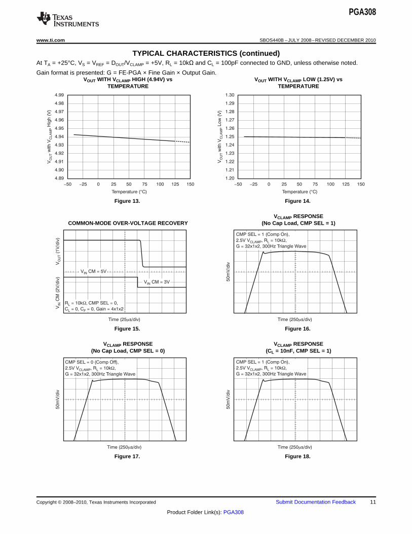
TYPICAL CHARACTERISTICSAt TA = +25°C, VS = VREF = DOUT/VCLAMP = +5V, RL = 10kΩ and CL = 100pF connected to GND, unless otherwise noted.
Gain format is presented: G = FE-PGA × Fine Gain × Output Gain.
FRONT-END PGA INPUT BIAS CURRENT FRONT-END PGA INPUT BIAS CURRENTWITH IPU ENABLED vs TEMPERATURE WITH IPU DISABLED vs TEMPERATURE
Figure 1. Figure 2.
COARSE OFFSET ADJUST ERROR vs FRONT-END PGA OFFSET VOLTAGE vsTEMPERATURE TEMPERATURE
Figure 3. Figure 4.
0.1Hz TO 10Hz OUTPUT NOISE INPUT-REFERRED FRONT-END NOISE vs(G = 1600) FREQUENCY
Figure 5. Figure 6.
Copyright © 2008–2010, Texas Instruments Incorporated Submit Documentation Feedback 9
Product Folder Link(s): PGA308

Temperature ( C)°
-50 15010075 1250-25 5025
0
-1
-2
-3
-4
-5
-6
-7
-8
-9
-10
Ove
r-S
ca
le T
ota
l E
rro
r (m
V)
Eight Programming Levels Shown
OS6 OS7 OS5
OS2
OS0 OS1 OS3, OS4
Temperature ( C)°
-50 15010075 1250-25 5025
14
12
10
8
6
4
2
0
Un
de
r-S
ca
le T
ota
l E
rro
r (m
V)
Eight Programming Levels Shown
US0
US6US5
US7
US1
US2 US3 US4
Temperature (°C)
-50 15010075 125-25 500 25
0.2
0
-0.2
-0.4
-0.6
-0.8
-1.0
-1.2
-1.4
-1.6
-1.8
-2.0
Off
se
t E
rro
r fr
om
Id
ea
l V
alu
e (
mV
)
156mV
2.344V
4.844V
Frequency (Hz)
10 10k1k100
120
110
100
90
80
70
60
50
CM
R (
dB
)
G = 4x1x2
G = 32x1x2
G = 100x1x2
G = 600x1x2
Frequency (Hz)
10 10k1k100
120
110
100
90
80
70
60
50
PS
RR
(d
B)
G = 100x1x2G = 600x1x2
G = 32x1x2
G = 4x1x2
Frequency (Hz)
1k 10M100k 1M10k
10000
1000
100
10
1
0.1
Ga
in
G = 800x1x2
G = 400x1x2
G = 32x1x3
G = 4x1x2
G = 1600x1x6
PGA308
SBOS440B –JULY 2008–REVISED DECEMBER 2010 www.ti.com
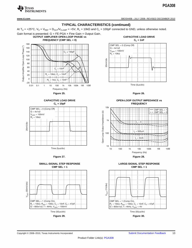
TYPICAL CHARACTERISTICS (continued)At TA = +25°C, VS = VREF = DOUT/VCLAMP = +5V, RL = 10kΩ and CL = 100pF connected to GND, unless otherwise noted.
Gain format is presented: G = FE-PGA × Fine Gain × Output Gain.OVER-SCALE TOTAL ERROR vs TEMPERATURE UNDER-SCALE TOTAL ERROR vs TEMPERATURE
(5V Ref) (4V Ref)
Figure 7. Figure 8.
ZERO DAC OFFSET ERROR vs COMMON-MODE REJECTION (RTI) vsTEMPERATURE FREQUENCY
Figure 9. Figure 10.
POWER-SUPPLY REJECTION RATIO (RTI) vs GAIN vsFREQUENCY FREQUENCY
Figure 11. Figure 12.
10 Submit Documentation Feedback Copyright © 2008–2010, Texas Instruments Incorporated
Product Folder Link(s): PGA308
Temperature (°C)
-50 15010075 1250-25 5025
4.99
4.98
4.97
4.96
4.95
4.94
4.93
4.92
4.91
4.90
4.89
Vw
ith
VH
igh
(V
)O
UT
CL
AM
P
Temperature ( C)°
-50 15010075 1250-25 5025
1.30
1.29
1.28
1.27
1.26
1.25
1.24
1.23
1.22
1.21
1.20
Vw
ith
VL
ow
(V
)O
UT
CL
AM
P
V(1
V/d
iv)
OU
TV
CM
(2
V/d
iv)
IN
Time (25 s/div)m
R = 10k CMP SEL = 0,W,L
C = 0, C = 0,L F Gain = 4x1x2
V CM = 5VIN
V CM = 3VIN
50
mV
/div
Time (250 s/div)m
CMP SEL = 1 (Comp On),
2.5V V , RCLAMP L = 10k ,W
G = 32x1x2, 300Hz Triangle Wave
50
mV
/div
Time (250 s/div)m
CMP SEL = 0 (Comp Off),
2.5V V , RCLAMP L = 10k ,W
G = 32x1x2, 300Hz Triangle Wave
50
mV
/div
Time (250 s/div)m
CMP SEL = 1 (Comp On),
2.5V V , RCLAMP L = 10kW,
G = 32x1x2, 300Hz Triangle Wave
PGA308
www.ti.com SBOS440B –JULY 2008–REVISED DECEMBER 2010
TYPICAL CHARACTERISTICS (continued)At TA = +25°C, VS = VREF = DOUT/VCLAMP = +5V, RL = 10kΩ and CL = 100pF connected to GND, unless otherwise noted.
Gain format is presented: G = FE-PGA × Fine Gain × Output Gain.VOUT WITH VCLAMP HIGH (4.94V) vs VOUT WITH VCLAMP LOW (1.25V) vs
TEMPERATURE TEMPERATURE
Figure 13. Figure 14.
VCLAMP RESPONSECOMMON-MODE OVER-VOLTAGE RECOVERY (No Cap Load, CMP SEL = 1)
Figure 15. Figure 16.
VCLAMP RESPONSE VCLAMP RESPONSE(No Cap Load, CMP SEL = 0) (CL = 10nF, CMP SEL = 1)
Figure 17. Figure 18.
Copyright © 2008–2010, Texas Instruments Incorporated Submit Documentation Feedback 11
Product Folder Link(s): PGA308

50
mV
/div
Time (250 s/div)m
CMP SEL = 0 (Comp Off),
2.5V V , RCLAMP L = 10k ,W
G = 32x1x2, 300Hz Triangle Wave
VS
V 0.1-S
V 0.2-S
V 0.3-S
V 0.4-S
GND + 0.4
GND + 0.3
GND + 0.2
GND + 0.1
GND
0 3 6 9 12 15
| Output Current | (mA)
Outp
ut V
olta
ge (
V)
V = 2.7VS V = 5.5VSV = 3VS V = 5VS
Temperature ( C)°
-50 15010075 1250-25 5025
1.6
1.4
1.2
1.0
0.8
0.6
0.4
0.2
0
I(m
A)
Q
Frequency (Hz)
0.01 10M1M100k10k1k1001010.1
120
100
80
60
40
20
0
-20
Ou
tpu
t A
mp
lifie
r O
pe
n-L
oo
p G
ain
(d
B)
C = 10nFL
RL L= 10kW, C = 10nF
RL L= 1kW, C = 10nF
CL £ 100pF
Frequency (Hz)
0.01 10M1M100k10k1k1001010.1
120
100
80
60
40
20
0
-20
Ou
tpu
t A
mp
lifie
r O
pe
n-L
oo
p G
ain
(d
B)
C = 10nFL
R = 10k , CWL L = 10nF
R = 1k , CWL L = 10nF
C 100pFL £
Frequency (Hz)
0.01 10M1M100k10k1k1001010.1
180
160
140
120
100
80
60
40
20
0
-20
Ou
tpu
t A
mp
lifie
r O
pe
n-L
oo
p P
ha
se
()
°
C = 10nFL
R = 10k , CWL L = 10nF
R = 1k , CWL L = 10nF
C 100pF£L
PGA308
SBOS440B –JULY 2008–REVISED DECEMBER 2010 www.ti.com
TYPICAL CHARACTERISTICS (continued)At TA = +25°C, VS = VREF = DOUT/VCLAMP = +5V, RL = 10kΩ and CL = 100pF connected to GND, unless otherwise noted.
Gain format is presented: G = FE-PGA × Fine Gain × Output Gain.VCLAMP RESPONSE OUTPUT VOLTAGE vs
(CL = 10nF, CMP SEL = 0) OUTPUT CURRENT
Figure 19. Figure 20.
QUIESCENT CURRENT vs OUTPUT AMPLIFIER OPEN-LOOP GAIN vsTEMPERATURE FREQUENCY (CMP SEL = 1)
Figure 21. Figure 22.
OUTPUT AMPLIFIER OPEN-LOOP GAIN vs OUTPUT AMPLIFIER OPEN-LOOP PHASE vsFREQUENCY (CMP SEL = 0) FREQUENCY (CMP SEL = 1)
Figure 23. Figure 24.
12 Submit Documentation Feedback Copyright © 2008–2010, Texas Instruments Incorporated
Product Folder Link(s): PGA308
20
mV
/div
Time (5 s/div)m
CMP SEL = 0 (Comp Off)
G = 4x1x2
V = 100mVOPP
RL = 10kW
Frequency (Hz)
0.01 10M1M100k10k1k1001010.1
180
160
140
120
100
80
60
40
20
0
-20
Ou
tpu
t A
mp
lifie
r O
pe
n-L
oo
p P
ha
se
()
°
C = 10nFL
RL L= 10kW, C = 10nF
RL L= 1kW, C = 10nF
CL £ 100pF
20
mV
/div
Time (5 s/div)m
CMP SEL = 0 (Comp Off)
G = 4x1x2
V = 100mVOPP
RL = 10kW
Frequency (Hz)
10 100 1k 10k 100k 1M 10M
10k
1k
100
10
Open-L
oop O
utp
ut Im
pedance (
)W
I = 0L
IL = 500mA
I = 5mAL
CMP SEL = 1CMP SEL = 0
V(5
0m
V/d
iv)
OU
T
Time (50 s/div)m
CMP SEL = 1 (Comp On),
R = 10k R = 100 ,L ISOW, W C = 10nF, CL F = 47pF,
G = 600x1x2, f = 4kHz, V = 100mVOPP
V(1
V/d
iv)
OU
T
Time (50 s/div)m
CMP SEL = 1 (Comp On),
R = 10k R = 100 ,L ISOW, W C = 10nF, CL F = 47pF,
G = 600x1x2, f = 4kHz, V = 4VOPP
PGA308
www.ti.com SBOS440B –JULY 2008–REVISED DECEMBER 2010
TYPICAL CHARACTERISTICS (continued)At TA = +25°C, VS = VREF = DOUT/VCLAMP = +5V, RL = 10kΩ and CL = 100pF connected to GND, unless otherwise noted.
Gain format is presented: G = FE-PGA × Fine Gain × Output Gain.OUTPUT AMPLIFIER OPEN-LOOP PHASE vs CAPACITIVE LOAD DRIVE
FREQUENCY (CMP SEL = 0) CL = 1nF
Figure 25. Figure 26.
CAPACITIVE LOAD DRIVE OPEN-LOOP OUTPUT IMPEDANCE vsCL = 10pF FREQUENCY
Figure 27. Figure 28.
SMALL-SIGNAL STEP RESPONSE LARGE-SIGNAL STEP RESPONSECMP SEL = 1 CMP SEL = 1
Figure 29. Figure 30.
Copyright © 2008–2010, Texas Instruments Incorporated Submit Documentation Feedback 13
Product Folder Link(s): PGA308

V(5
0m
V/d
iv)
OU
T
Time (50 s/div)m
CMP SEL = 1 (Comp On),
R = 10k R = 100 ,L ISOW, W C = 10nF, CL F = 47pF,
G = 4x1x2, f = 4kHz, V = 100mVOPP
V(1
V/d
iv)
OU
T
Time (50 s/div)m
CMP SEL = 1 (Comp On),
R = 10k R = 100 ,L ISOW, W C = 10nF, CL F = 47pF,
G = 4x1x2, f = 4kHz, V = 4VOPP
VO
UT
(50
mV
/div
)
Time (50ms/div)
CMP SEL = 0 (Comp Off),
R = 10kL LW, C = 0, C = 0,F
G = 600x1x2, f = 4kHz, VOPP = 100mV
V(1
V/d
iv)
OU
T
Time (50 s/div)m
CMP SEL = 0 (Comp Off),
R = 10kL W, C = 0, CL F = 0,
G = 600x1x2, f = 4kHz, V = 4VOPP
V(5
0m
V/d
iv)
OU
T
Time (50 s/div)m
CMP SEL = 0 (Comp Off),
R = 10kL W, C = 0, C = 0,L F
G = 4x1x2, f = 4kHz, V = 100mVOPP
V(1
V/d
iv)
OU
T
Time (50 s/div)m
CMP SEL = 0 (Comp Off),
R = 10kL W, C = 0, C = 0,L F
G = 4x1x2, f = 4kHz, V = 4VOPP
PGA308
SBOS440B –JULY 2008–REVISED DECEMBER 2010 www.ti.com
TYPICAL CHARACTERISTICS (continued)At TA = +25°C, VS = VREF = DOUT/VCLAMP = +5V, RL = 10kΩ and CL = 100pF connected to GND, unless otherwise noted.
Gain format is presented: G = FE-PGA × Fine Gain × Output Gain.SMALL-SIGNAL STEP RESPONSE LARGE-SIGNAL STEP RESPONSE
CMP SEL = 1 CMP SEL = 1
Figure 31. Figure 32.
SMALL-SIGNAL STEP RESPONSE LARGE-SIGNAL STEP RESPONSECMP SEL = 0 CMP SEL = 0
Figure 33. Figure 34.
SMALL-SIGNAL STEP RESPONSE LARGE-SIGNAL STEP RESPONSECMP SEL = 0 CMP SEL = 0
Figure 35. Figure 36.
14 Submit Documentation Feedback Copyright © 2008–2010, Texas Instruments Incorporated
Product Folder Link(s): PGA308
PGA308
www.ti.com SBOS440B –JULY 2008–REVISED DECEMBER 2010
FUNCTIONAL DESCRIPTION
OVERVIEW VOLTAGE REFERENCE
The PGA308 is an ideal building block for resistive The PGA308 VREF pin provides input from abridge sensor conditioning and general data reference voltage. The reference voltage is used byacquisition. Digitally-programmable coarse offset, fine the Coarse Offset Adjust and Zero DACs. The faultoffset, and gain may be controlled in real time or monitor circuitry trip points, as well as the over- andpermanently programmed into the PGA308. under-scale limits, can be selected to be referenced
to either VS or VREF. This flexibility accommodatesabsolute or ratiometric mode designs.SENSOR ERROR ADJUSTMENT RANGE
The PGA308 is designed to readily accommodate the FAULT MONITOR CIRCUIT SENSOR FAULTfollowing sensors: DETECTION
Span25°C: 0.08mV/V to 296mV/VTo detect sensor burnout and/or short, a set of fourInitial Offset: 20mV/Vcomparators (external fault comparators) are
Span and offset are based on a bridge sensor connected to the inputs of the front-end PGA. Thereexcitation voltage of +5V, a PGA308 output voltage are two fault-detect modes of operation for thesespan of 4V (+0.5V to +4.5V), VREF of +5V, and a comparators.VOUT/VIN gain up to 9600. For proper PGA308 setup,consider noise, small-signal bandwidth, VOUT/VIN Common-Mode Faultgain, and required system error.
If either of the inputs are taken outside of thecommon-mode range of the amplifier [greater thanAMPLIFICATION SIGNAL PATH (VS – 1.2V), or less than 100mV], then thecorresponding comparator sets a sensor fault flagThe core of the PGA308 is a precision, low drift, andthat can be programmed to drive the PGA308 VOUT tolow noise front-end programmable gain amplifierwithin 100mV (IOUT < 4mA) of either VS (or VCLAMP if(PGA). This front-end PGA has gain capabilities fromVCLAMP is used) or ground. This level is well abovex4 to x1600. The output amplifier has a gain rangethe set over-scale limit level or well below the setfrom ×2 to ×6. A fine gain adjust in front of the outputunder-scale limit level. The state of the fault conditionamplifier offers a selectable ×0.33 to ×1.0 attenuationcan be read in digital form in the ALRM register. If thefactor. This architecture yields a VOUT/VIN gain rangeover-scale/under-scale limiting is disabled, thefor the PGA309 of ×2.67 to ×9600. Many applicationsPGA308 output voltage is also driven within 100mVuse overall gains of ×1600 or less. The selection of(IOUT < 4mA) of either VS (or VCLAMP if VCLAMP is used)gains in the front-end PGA and output amplifier,or ground, depending on the selected fault polarityalthough capable of up to ×9600 overall gain, are(high or low).intended to allow for gain distribution throughout the
PGA308; this design enables optimum span andBridge Faultoffset scaling from input to output. The polarity of the
inputs can be switched through the input mux to To assist in identifying mis-wiring, or open- oraccommodate sensors with unknown polarity output. short-circuit conditions, the PGA308 provides bridgeHigher gains reduce bandwidth and require more fault monitoring. For bridge fault detection, either VSanalog filtering and/or system analog-to-digital or VREF (whichever is used for bridge excitation) canconverter (ADC) averaging to reject noise. be chosen as VFLT. If either of the inputs are taken to
less than the larger of either 100mV or 0.35VFLT, thenCOARSE AND FINE OFFSET ADJUSTMENT a fault is signaled. Also, if either of the inputs is taken
to greater than the smaller of (VS – 1.2V) or 0.65VFLT,The sensor offset adjustment is done in two stages.then a fault is signaled. This fault detection allows forThe input-referred Coarse Offset Adjust DAC has aoperation with bridge differential voltages of up to±100mV offset adjustment range for a selected VREF30% of the bridge excitation voltage. Theof +5V. Any residual input sensor offset is correctedcorresponding comparator sets a sensor fault flagand any desired VOUT offset pedestal for zero-appliedthat can be programmed to drive the PGA308 VOUT tosensor strain input is set by a Fine Offset Adjustwithin 100mV (IOUT < 4mA) of either VS (or VCLAMP ifthrough the 16-bit Zero DAC that adds to the signalVCLAMP is used) or ground. This level is well abovefrom the output of the front-end PGA.the set over-scale limit level or well below the set
Copyright © 2008–2010, Texas Instruments Incorporated Submit Documentation Feedback 15
Product Folder Link(s): PGA308

PGA308
SBOS440B –JULY 2008–REVISED DECEMBER 2010 www.ti.com
under-scale limit level. If over-scale/under-scale DIGITAL INTERFACE: ONE-WIRE PROGRAMlimiting is disabled, the PGA308 output voltage is PROTOCOLdriven within 100mV (IOUT < 4mA) of either VS or
The PGA308 can be configured through a single-wire,ground, depending on the selected fault polarity (highUART-compatible interface (1W pin). It is possible toor low).connect this single-wire communication pin to theVOUT pin in true three-terminal modules (VS, ground,Additional Fault Detectionand sensor out) and continue to allow for calibration
There are five additional fault detect comparators and configuration programming.(internal fault comparators) that help detect subtle
All communication transactions start with anPGA308 front-end violations that could result in linearinitialization byte transmitted by the controller. Thisvoltages at VOUT and be interpreted as valid states.byte (55h) sets the baud rate used for theThese comparators are especially useful duringcommunication transaction. The baud rate is sensedfactory calibration and setup.during the initialization byte of every transaction, andis used throughout the entire transaction. EachAlarm Registertransaction may use a different baud rate, if desired.
Each of nine fault conditions sets a corresponding bit Baud rates of 4.8k to 114k bits/second are supported.in the Alarm register. The state of the fault condition
Each communication consists of several bytes ofcan be read digitally from the Alarm register.data. Each byte consists of 10-bit periods. The first bitis the start bit and is always '0'. When idle, the 1WOVER-SCALE AND UNDER-SCALE LIMITS pin should always be high. The second through ninthbits are the eight data bits for the byte and areThe over-scale and under-scale limit circuitrytransferred LSB first. The 10th bit is the stop bit andprovides a programmable upper and lower clip limitis always '1'.for the PGA308 output voltage. When combined with
the fault monitor circuitry, system diagnostics can be The second byte is a command/address byte. Theperformed to determine if a conditioned sensor is last bit in this byte indicates either a read or write atdefective, or if the process being monitored by the the address selected by the address pointer portionsensor is out of range. The selected PGA308 VLIM is of the byte. Additional data transfer occurs after thedivided down by a precision resistor string to form the command/address byte. The number of bytes andover- and under-scale trip points. These resistor direction of data transfer depend on the commandratios are extremely accurate and produce no byte. For a read sequence, the PGA308 waits for asignificant initial or temperature errors. An over-scale 2-bit delay (unless programmed otherwise) after theamplifier driven by the over-scale threshold limits completion of the command/address byte before(clips) the maximum PGA308 output, VOUT. Similarly, beginning to transmit. This wait allows time for thean under-scale amplifier driven by the under-scale controller to ensure that the PGA308 is able to controlthreshold limits (clips) the minimum PGA308 output, the One-Wire interface. The first byte transmitted byVOUT. The reference for the trip points, VLIM, is the PGA308 is the least significant byte of the registerregister-selectable for either VREF or VS. and the second byte will be the most significant byte
of the register.DOUT/VCLAMP PIN
The recommended circuit implementation is to use aThe dual-use DOUT/VCLAMP pin functions either as a pull-up resistor and/or current source with an openVOUT clamp or as a digital push-pull output. The drain (or open collector) output connected to the 1Wvoltage clamp function provides an output voltage pin, which is also an open drain output. The singleclamp, which is external-resistor programmable. In wire can be driven high by the controller duringmixed-voltage systems, where the PGA308 may run transmit from the controller, but some form of pull-upfrom +5V with its output scaled for 0.1V to 2.9V, is required to allow the signal to go high duringVCLAMP can be set to 3.0V to prevent an over-voltage receive because the PGA308 1W pin can only pulllock-up/latch-up condition on a 3V system ADC or the output low.microcontroller input. When programmed as a digitaloutput this pin can be used for sensor moduleconfiguration. The value may be pre-programmed inthe one-time programmable (OTP) banks, orcontrolled through the One-Wire interface (1W pin).
16 Submit Documentation Feedback Copyright © 2008–2010, Texas Instruments Incorporated
Product Folder Link(s): PGA308

PGA308
www.ti.com SBOS440B –JULY 2008–REVISED DECEMBER 2010
Timeout on the One-Wire Interface ONE-WIRE OPERATION WITH 1WCONNECTED TO VOUTThe PGA308 includes a timeout mechanism. If
synchronization between the controller and the In some sensor applications, it is desired to providePGA308 is lost for any reason, the timeout the end user of the sensor module with three pins:mechanism allows the One-Wire interface to reset VS, GND, and Sensor Out. It is also desired in thesecommunication. The timeout period is set to applications to digitally calibrate the sensor moduleapproximately 28ms (typical). If the timeout period after its final assembly of sensor and electronics. Theexpires between the initialization byte and the PGA308 has a mode that allows the One-Wirecommand byte, between the command byte and any interface pin (1W) to be tied directly to the PGA308data byte, or between any data bytes, the PGA308 output pin (VOUT).resets the One-Wire interface circuitry so that it
To calibrate the PGA308 in Three-Wire configuration,expects an initialization byte. Every time that a byte isprogram the internal registers and measure thetransmitted on the single wire interface, this timeoutresulting VOUT. To do this while VOUT is connected toperiod restarts.1W requires the ability to enable and disable VOUT.Thus, the 1W/VOUT line operates in a multiplexedPOWER-ON SEQUENCEmode where 1W is used as a bidirectional digital
The PGA308 provides circuitry to detect when the interface while VOUT is disabled, and VOUT drives thepower supply is applied to the PGA308 and resets line as a conditioned sensor output voltage when it isthe internal registers to a known power-on reset enabled.(POR) state. This reset also occurs whenever the
The PGA308 also provides a mode in which thesupply is invalid so that the PGA308 is set to a knownoutput amplifier can be enabled for a set time periodstate when the supply becomes valid again. Theand then disabled again to allow sharing of the 1Wthreshold for this circuit is approximately 1.7V topin with the VOUT connection. This action is2.1V. After the power supply becomes valid, theaccomplished by writing a value to bits OEN[7:0] inPGA308 waits for approximately 25ms, during whichthe One-Wire Enable Control register (OENC). AnyVOUT is disabled, and then attempts to read the datanon-zero value enables the output. This non-zerofrom the last valid OTP memory bank. If the memoryvalue is decremented every 10ms until it becomesbank has the proper checksum, then the PGA308zero. When this value becomes zero, VOUT isRAM is loaded with the OTP data and VOUT enabled.disabled and a 1s timeout begins waiting for busIf the checksum is invalid, VOUT is set to disabled.activity on the digital interface (1W pin). As long asUnless disabled by the OWD bit in Configurationthere is activity on the 1W pin, the 1s timeout isRegister 2 (CFG2), the One-Wire interface cancontinually reset. After 1s of no bus activity, thealways communicate to the PGA308 and override thePGA308 checks for a correct checksum. If thecontents of the current RAM in use by setting thechecksum is correct, the PGA308 runs with theappropriate SWL[2:0] bits in the Software Controlvalues that currently exist in RAM. If the checksum isRegister (SFTC). For applications that requirenot valid, the PGA308 checks for written bank selectinstant-on for VOUT, the NOW bit in the CFG2 registerregisters in OTP in the order of BANK SEL4, BANKcan be set to '1', which eliminates the 25ms disableSEL3, BANK SEL2 then BANK SEL1. The highestof VOUT on power-up.bank select register containing valid programmed
space data is read. The value read from this register pointsto one of the seven OTP banks, which is then loaded
space into RAM.space spacespace spacespace spacespace
space
Copyright © 2008–2010, Texas Instruments Incorporated Submit Documentation Feedback 17
Product Folder Link(s): PGA308

V = mux_sign V + V GI + V GD GOOUT IN Coarse_Offset Zero_DAC[ ]? ? ? ?( (
PGA308
SBOS440B –JULY 2008–REVISED DECEMBER 2010 www.ti.com
OTP MEMORY BANKS PGA308 TRANSFER FUNCTION
There are four one-time programmable (OTP) bank Equation 1 shows the mathematical expression that isselection registers: BANK SEL1, BANK SEL2, BANK used to compute the output voltage, VOUT. ThisSEL3, and BANK SEL4. Bank selection may be set equation can also be rearranged algebraically tofour times by programming the BANK SELx registers solve for different terms. For example, duringin order (1, 2, 3, 4). The default OTP bank used on calibration, this equation is rearranged to solve forPOR is the location stored in the last programmed VIN.BANK SELx register. Therefore, if programmed,BANK SEL4 always has priority over lower-numbered
(1)bank select registers.Where:The PGA308 contains seven OTP user memory
mux_sign: This term changes the polarity of thebanks. All seven of these banks may beinput signal; value is ±1independently programmed. However, the default
bank at POR can be set only four times. The seven VIN: The input signal for the PGA308; VIN1 = VINP,possible OTP user memory banks allow an end VIN2 = VINNproduct with a microcontroller interface between the VCoarse_Offset: The coarse offset DAC outputend-user and the PGA308 to select from up to seven voltagefactory pre-programmed configurations. It also
GI: Input stage gainprovides total user flexibility for any otherVZero_DAC: Zero DAC output voltageconfiguration through software communication over
the One-Wire interface (1W pin). This flexibility allows GD: Gain DACno-scrap recovery from miscalibration situations. GO: Output stage gain
18 Submit Documentation Feedback Copyright © 2008–2010, Texas Instruments Incorporated
Product Folder Link(s): PGA308

Control Registers
RAM
Alarm Register
RF
RF
RG
R
R
8R
VREF
4R
4R
8R
3
Auto
Zero
Auto
Zero
Auto
Zero
Output
Amplifier
Input Mux
VINN
VINP
A2
A1
A3Front-End
PGA Gain
PGA
Diff Amp
NOTES: (1) User-adjustable feature.
(2) Optional connection; see the section for more information.One-Wire Operation with 1W Connected to VOUT
(3) Optional connection; see the PGA308 User's Guide for more information.
RGO
VOUT FILT
CF CL
VREF
VREF
VS
VREF
16-Bit DAC
0 < V < VZDAC REFInput Mux Control(1)
7-Bit + SignDAC
Coarse Offset Range(1)
Coarse Offset Adjust(1)
Fault MonitorCircuit
RefSelect
BridgeSensor
Zero DAC
Gain DACVIN1
VOS
VREF VS
VIN2
Fine Offset Adjust(1)
(16-Bit)
PGA Gain Select (1 of 16)(1)
Range of 4 to 1600
(w/PGA Diff Amp Gain = 4)
Front-End PGA Out
Gain = x4 to x1600
Offset Due to Zero DAC
-0.5V < Offset < +0.5VREF REF
Alarm Register Inputs
Output Gain Select (1-of-7)(1)
Range of 2 to 5
INT/EXT FB Select(1)
Fault RefSelect(1)
Fault Detect Mode(1)
Fine Gain Adjust (16-Bit)(1)
OS/US Ref Select(1)
DO
UT/V
CL
AM
P(1
)
DigitalControls
RFO
RISOVOUT
1
1
2
RCL1
RCL2
D /VOUT CLAMPVCLAMP
Mode
Only
1W
VFB
VSJ
Scale
Limit
Interface
and
Control
Circuitry
OTP
(7 Banks)
Clamp
VLIM
3-Bit DAC
Under-Scale Limit(1)
VLIM
VS
3-Bit DAC
Over-Scale Limit(1)
(2)
(3)
POR
VS
VS
Ref
Select
Dig
ital O
ut
VS
VREF
VLIM
VREF
GND
PGA308
PGA308
www.ti.com SBOS440B –JULY 2008–REVISED DECEMBER 2010
Figure 37. Detailed Block Diagram
Copyright © 2008–2010, Texas Instruments Incorporated Submit Documentation Feedback 19
Product Folder Link(s): PGA308

PGA308
SBOS440B –JULY 2008–REVISED DECEMBER 2010 www.ti.com
REVISION HISTORY
NOTE: Page numbers for previous revisions may differ from page numbers in the current version.
Changes from Revision A (April, 2009) to Revision B Page
• Updated front page format to current standards ................................................................................................................... 1
• Added PGA Transfer Function section ............................................................................................................................... 18
20 Submit Documentation Feedback Copyright © 2008–2010, Texas Instruments Incorporated
Product Folder Link(s): PGA308
PACKAGE OPTION ADDENDUM
www.ti.com 8-Jul-2016
Addendum-Page 1
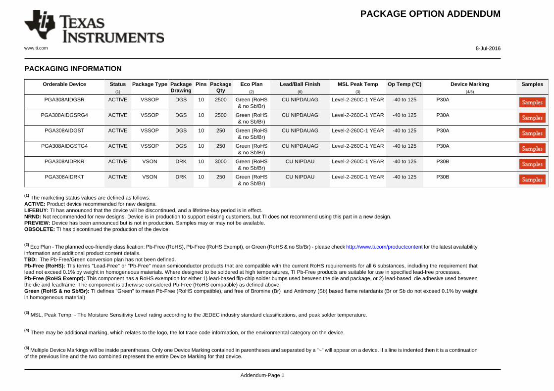
PACKAGING INFORMATION
Orderable Device Status(1)
Package Type PackageDrawing
Pins PackageQty
Eco Plan(2)
Lead/Ball Finish(6)
MSL Peak Temp(3)
Op Temp (°C) Device Marking(4/5)
Samples
PGA308AIDGSR ACTIVE VSSOP DGS 10 2500 Green (RoHS& no Sb/Br)
CU NIPDAUAG Level-2-260C-1 YEAR -40 to 125 P30A
PGA308AIDGSRG4 ACTIVE VSSOP DGS 10 2500 Green (RoHS& no Sb/Br)
CU NIPDAUAG Level-2-260C-1 YEAR -40 to 125 P30A
PGA308AIDGST ACTIVE VSSOP DGS 10 250 Green (RoHS& no Sb/Br)
CU NIPDAUAG Level-2-260C-1 YEAR -40 to 125 P30A
PGA308AIDGSTG4 ACTIVE VSSOP DGS 10 250 Green (RoHS& no Sb/Br)
CU NIPDAUAG Level-2-260C-1 YEAR -40 to 125 P30A
PGA308AIDRKR ACTIVE VSON DRK 10 3000 Green (RoHS& no Sb/Br)
CU NIPDAU Level-2-260C-1 YEAR -40 to 125 P30B
PGA308AIDRKT ACTIVE VSON DRK 10 250 Green (RoHS& no Sb/Br)
CU NIPDAU Level-2-260C-1 YEAR -40 to 125 P30B
(1) The marketing status values are defined as follows:ACTIVE: Product device recommended for new designs.LIFEBUY: TI has announced that the device will be discontinued, and a lifetime-buy period is in effect.NRND: Not recommended for new designs. Device is in production to support existing customers, but TI does not recommend using this part in a new design.PREVIEW: Device has been announced but is not in production. Samples may or may not be available.OBSOLETE: TI has discontinued the production of the device.
(2) Eco Plan - The planned eco-friendly classification: Pb-Free (RoHS), Pb-Free (RoHS Exempt), or Green (RoHS & no Sb/Br) - please check http://www.ti.com/productcontent for the latest availabilityinformation and additional product content details.TBD: The Pb-Free/Green conversion plan has not been defined.Pb-Free (RoHS): TI's terms "Lead-Free" or "Pb-Free" mean semiconductor products that are compatible with the current RoHS requirements for all 6 substances, including the requirement thatlead not exceed 0.1% by weight in homogeneous materials. Where designed to be soldered at high temperatures, TI Pb-Free products are suitable for use in specified lead-free processes.Pb-Free (RoHS Exempt): This component has a RoHS exemption for either 1) lead-based flip-chip solder bumps used between the die and package, or 2) lead-based die adhesive used betweenthe die and leadframe. The component is otherwise considered Pb-Free (RoHS compatible) as defined above.Green (RoHS & no Sb/Br): TI defines "Green" to mean Pb-Free (RoHS compatible), and free of Bromine (Br) and Antimony (Sb) based flame retardants (Br or Sb do not exceed 0.1% by weightin homogeneous material)
(3) MSL, Peak Temp. - The Moisture Sensitivity Level rating according to the JEDEC industry standard classifications, and peak solder temperature.
(4) There may be additional marking, which relates to the logo, the lot trace code information, or the environmental category on the device.
(5) Multiple Device Markings will be inside parentheses. Only one Device Marking contained in parentheses and separated by a "~" will appear on a device. If a line is indented then it is a continuationof the previous line and the two combined represent the entire Device Marking for that device.

PACKAGE OPTION ADDENDUM
www.ti.com 8-Jul-2016
Addendum-Page 2
(6) Lead/Ball Finish - Orderable Devices may have multiple material finish options. Finish options are separated by a vertical ruled line. Lead/Ball Finish values may wrap to two lines if the finishvalue exceeds the maximum column width.
Important Information and Disclaimer:The information provided on this page represents TI's knowledge and belief as of the date that it is provided. TI bases its knowledge and belief on informationprovided by third parties, and makes no representation or warranty as to the accuracy of such information. Efforts are underway to better integrate information from third parties. TI has taken andcontinues to take reasonable steps to provide representative and accurate information but may not have conducted destructive testing or chemical analysis on incoming materials and chemicals.TI and TI suppliers consider certain information to be proprietary, and thus CAS numbers and other limited information may not be available for release.
In no event shall TI's liability arising out of such information exceed the total purchase price of the TI part(s) at issue in this document sold by TI to Customer on an annual basis.
OTHER QUALIFIED VERSIONS OF PGA308 :
• Automotive: PGA308-Q1
NOTE: Qualified Version Definitions:
• Automotive - Q100 devices qualified for high-reliability automotive applications targeting zero defects
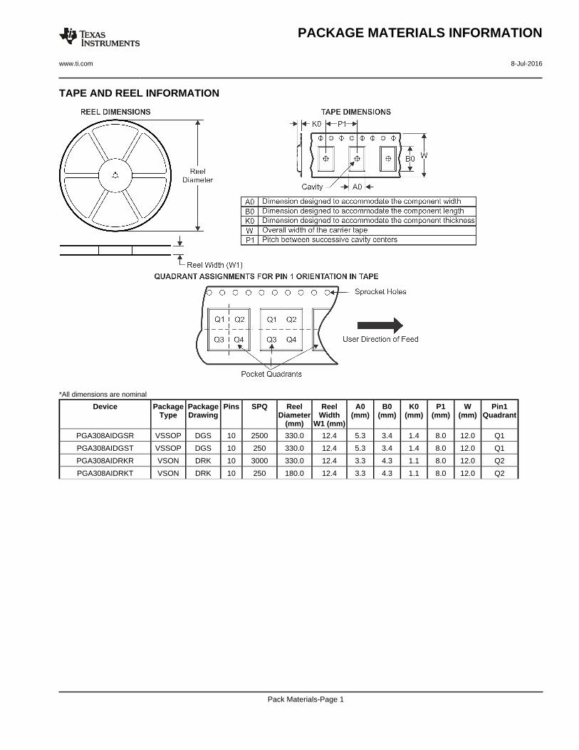
TAPE AND REEL INFORMATION
*All dimensions are nominal
Device PackageType
PackageDrawing
Pins SPQ ReelDiameter
(mm)
ReelWidth
W1 (mm)
A0(mm)
B0(mm)
K0(mm)
P1(mm)
W(mm)
Pin1Quadrant
PGA308AIDGSR VSSOP DGS 10 2500 330.0 12.4 5.3 3.4 1.4 8.0 12.0 Q1
PGA308AIDGST VSSOP DGS 10 250 330.0 12.4 5.3 3.4 1.4 8.0 12.0 Q1
PGA308AIDRKR VSON DRK 10 3000 330.0 12.4 3.3 4.3 1.1 8.0 12.0 Q2
PGA308AIDRKT VSON DRK 10 250 180.0 12.4 3.3 4.3 1.1 8.0 12.0 Q2
PACKAGE MATERIALS INFORMATION
www.ti.com 8-Jul-2016
Pack Materials-Page 1

*All dimensions are nominal
Device Package Type Package Drawing Pins SPQ Length (mm) Width (mm) Height (mm)
PGA308AIDGSR VSSOP DGS 10 2500 366.0 364.0 50.0
PGA308AIDGST VSSOP DGS 10 250 366.0 364.0 50.0
PGA308AIDRKR VSON DRK 10 3000 367.0 367.0 35.0
PGA308AIDRKT VSON DRK 10 250 210.0 185.0 35.0
PACKAGE MATERIALS INFORMATION
www.ti.com 8-Jul-2016
Pack Materials-Page 2


IMPORTANT NOTICE
Texas Instruments Incorporated and its subsidiaries (TI) reserve the right to make corrections, enhancements, improvements and otherchanges to its semiconductor products and services per JESD46, latest issue, and to discontinue any product or service per JESD48, latestissue. Buyers should obtain the latest relevant information before placing orders and should verify that such information is current andcomplete. All semiconductor products (also referred to herein as “components”) are sold subject to TI’s terms and conditions of salesupplied at the time of order acknowledgment.TI warrants performance of its components to the specifications applicable at the time of sale, in accordance with the warranty in TI’s termsand conditions of sale of semiconductor products. Testing and other quality control techniques are used to the extent TI deems necessaryto support this warranty. Except where mandated by applicable law, testing of all parameters of each component is not necessarilyperformed.TI assumes no liability for applications assistance or the design of Buyers’ products. Buyers are responsible for their products andapplications using TI components. To minimize the risks associated with Buyers’ products and applications, Buyers should provideadequate design and operating safeguards.TI does not warrant or represent that any license, either express or implied, is granted under any patent right, copyright, mask work right, orother intellectual property right relating to any combination, machine, or process in which TI components or services are used. Informationpublished by TI regarding third-party products or services does not constitute a license to use such products or services or a warranty orendorsement thereof. Use of such information may require a license from a third party under the patents or other intellectual property of thethird party, or a license from TI under the patents or other intellectual property of TI.Reproduction of significant portions of TI information in TI data books or data sheets is permissible only if reproduction is without alterationand is accompanied by all associated warranties, conditions, limitations, and notices. TI is not responsible or liable for such altereddocumentation. Information of third parties may be subject to additional restrictions.Resale of TI components or services with statements different from or beyond the parameters stated by TI for that component or servicevoids all express and any implied warranties for the associated TI component or service and is an unfair and deceptive business practice.TI is not responsible or liable for any such statements.Buyer acknowledges and agrees that it is solely responsible for compliance with all legal, regulatory and safety-related requirementsconcerning its products, and any use of TI components in its applications, notwithstanding any applications-related information or supportthat may be provided by TI. Buyer represents and agrees that it has all the necessary expertise to create and implement safeguards whichanticipate dangerous consequences of failures, monitor failures and their consequences, lessen the likelihood of failures that might causeharm and take appropriate remedial actions. Buyer will fully indemnify TI and its representatives against any damages arising out of the useof any TI components in safety-critical applications.In some cases, TI components may be promoted specifically to facilitate safety-related applications. With such components, TI’s goal is tohelp enable customers to design and create their own end-product solutions that meet applicable functional safety standards andrequirements. Nonetheless, such components are subject to these terms.No TI components are authorized for use in FDA Class III (or similar life-critical medical equipment) unless authorized officers of the partieshave executed a special agreement specifically governing such use.Only those TI components which TI has specifically designated as military grade or “enhanced plastic” are designed and intended for use inmilitary/aerospace applications or environments. Buyer acknowledges and agrees that any military or aerospace use of TI componentswhich have not been so designated is solely at the Buyer's risk, and that Buyer is solely responsible for compliance with all legal andregulatory requirements in connection with such use.TI has specifically designated certain components as meeting ISO/TS16949 requirements, mainly for automotive use. In any case of use ofnon-designated products, TI will not be responsible for any failure to meet ISO/TS16949.
Products ApplicationsAudio www.ti.com/audio Automotive and Transportation www.ti.com/automotiveAmplifiers amplifier.ti.com Communications and Telecom www.ti.com/communicationsData Converters dataconverter.ti.com Computers and Peripherals www.ti.com/computersDLP® Products www.dlp.com Consumer Electronics www.ti.com/consumer-appsDSP dsp.ti.com Energy and Lighting www.ti.com/energyClocks and Timers www.ti.com/clocks Industrial www.ti.com/industrialInterface interface.ti.com Medical www.ti.com/medicalLogic logic.ti.com Security www.ti.com/securityPower Mgmt power.ti.com Space, Avionics and Defense www.ti.com/space-avionics-defenseMicrocontrollers microcontroller.ti.com Video and Imaging www.ti.com/videoRFID www.ti-rfid.comOMAP Applications Processors www.ti.com/omap TI E2E Community e2e.ti.comWireless Connectivity www.ti.com/wirelessconnectivity
Mailing Address: Texas Instruments, Post Office Box 655303, Dallas, Texas 75265Copyright © 2016, Texas Instruments Incorporated