single photon emission from silicon-vacancy colour centres in
TRANSCRIPT

OPEN ACCESS
Single photon emission from silicon-vacancycolour centres in chemical vapour depositionnano-diamonds on iridiumTo cite this article: Elke Neu et al 2011 New J. Phys. 13 025012
View the article online for updates and enhancements.
Related contentLow-temperature investigations of singlesilicon vacancy colour centres in diamondElke Neu, Christian Hepp, MichaelHauschild et al.
-
Diamond-based single-photon emittersI Aharonovich, S Castelletto, D A Simpsonet al.
-
Single photon emission from SiV centresin diamond produced by ion implantationChunlang Wang, Christian Kurtsiefer,Harald Weinfurter et al.
-
Recent citationsThe heat is on: towards the realization ofnon-cryogenic photonic quantumtechnologiesMark J Holmes and Yasuhiko Arakawa
-
Spectroscopic investigations of negativelycharged tin-vacancy centres in diamondJohannes Görlitz et al
-
Intrinsic exciton transitions of isotopicallypurified 13C studied by photoluminescenceand transmission spectroscopyRyota Ishii et al
-
This content was downloaded from IP address 36.234.221.135 on 06/10/2021 at 04:39

T h e o p e n – a c c e s s j o u r n a l f o r p h y s i c s
New Journal of Physics
Single photon emission from silicon-vacancy colourcentres in chemical vapour depositionnano-diamonds on iridium
Elke Neu1, David Steinmetz1, Janine Riedrich-Möller1,Stefan Gsell2, Martin Fischer2, Matthias Schreck2
and Christoph Becher1,3
1 Universität des Saarlandes, Fachrichtung 7.2 (Experimentalphysik),Campus E2.6, 66123 Saarbrücken, Germany2 Universität Augsburg, Lehrstuhl für Experimentalphysik IV,Universitätsstrasse 1 (Gebäude Nord), 86135 Augsburg, GermanyE-mail: [email protected]
New Journal of Physics 13 (2011) 025012 (21pp)Received 27 August 2010Published 21 February 2011Online at http://www.njp.org/doi:10.1088/1367-2630/13/2/025012
Abstract. We introduce a process for the fabrication of high-quality, spatiallyisolated nano-diamonds on iridium via microwave-plasma-assisted chemicalvapour deposition (CVD) growth. We perform spectroscopy of single silicon-vacancy (SiV) centres produced during the growth of the nano-diamonds. Thecolour centres exhibit extraordinary narrow zero-phonon-lines down to 0.7 nm atroom temperature. Single photon count rates up to 4.8 Mcps at saturation makethese SiV centres the brightest diamond-based single photon sources to date. Wemeasure for the first time the fine structure of a single SiV centre, thus confirmingthe atomic composition of the investigated colour centres.
3 Author to whom any correspondence should be addressed.
New Journal of Physics 13 (2011) 0250121367-2630/11/025012+21$33.00 © IOP Publishing Ltd and Deutsche Physikalische Gesellschaft

2
Contents
1. Introduction 22. Experimental 4
2.1. Sample preparation . . . . . . . . . . . . . . . . . . . . . . . . . . . . . . . . 42.2. Experimental setup . . . . . . . . . . . . . . . . . . . . . . . . . . . . . . . . 5
3. Results 63.1. Single emitter spectroscopy at room temperature . . . . . . . . . . . . . . . . 63.2. Single emitter spectroscopy at cryogenic temperatures . . . . . . . . . . . . . . 18
4. Conclusion 19Acknowledgments 20References 20
1. Introduction
Single photon sources are of great interest for various applications in quantum information,in particular quantum cryptography (e.g. [1]). In recent years, colour centres in diamond havebeen proven to have the potential to fulfil the requirements for practical single photon sources,such as room temperature operation, photostability and high brightness. Nitrogen-vacancy(NV) centres [2]–[4], nickel-based NE8 centres [5]–[8], nickel–silicon complexes [9, 10],chromium-related colour centres [11, 12] as well as silicon-vacancy (SiV) centres [13] havebeen employed as single photon sources. The majority of the experiments have been performedon NV centres as they are easily available in single crystal diamonds [2] and in nano-diamonds [3], either produced during the growth process or by ion implantation. In addition, dueto the extraordinarily long spin coherence times, key experiments towards quantum informationprocessing have been realized with NV centres, e.g. two-qubit quantum gates [14] or quantumregisters based on NV spins [15]. However, NV centres possess the detrimental property of aroom temperature emission width of about 100 nm due to strong phonon coupling.
SiV centres were suggested as an alternative to NV centres due to their narrow zero-phonon-line (ZPL) width of 5 nm at room temperature, their low phonon coupling [13], aswell as their feasible creation by ion implantation or during chemical vapour deposition(CVD) growth [18]. A further advantage is their emission in the near infrared at 738 nm ina spectral region where the background fluorescence of the surrounding diamond material isweak. First single emitter experiments on SiV centres created by ion implantation in naturaldiamonds [13], however, revealed unfavourable low single photon emission rates of the orderof only 1000 counts s−1, despite a short lifetime of 1.2 ns. Radiative quantum yields of only0.05 were found for SiV centres in CVD films [19] and were explained by temperature-dependent non-radiative transitions, indicated by a strong increase in luminescence intensityfor temperatures below 100 K [20]. Furthermore, the luminescence of SiV centres is quenchedby the presence of graphite [16], thus defining the need for high-purity diamonds.
The structure of the SiV centre has been intensively investigated: it most probably consistsof a silicon atom and a lattice vacancy arranged in a so-called ‘split-vacancy configuration’,where a substitutional silicon atom relaxes its position towards a neighbouring vacancy [21],as illustrated in figure 1. Photoluminescence excitation measurements suggest a position of theground state of the centre 2.05 eV below the conduction band edge [16]. Spectroscopy of a
New Journal of Physics 13 (2011) 025012 (http://www.njp.org/)

3
48 GHz
242 GHz
Conduction Band
2.05 eV
ZPL1.68 eV
Si
C
(a) (b)
Figure 1. (a) Proposed structure of the SiV centre with a silicon atom in a split-vacancy site. (b) Level scheme of the SiV centre according to [16, 17]. Theoptical transitions are not drawn to scale.
high-quality single crystalline diamond at cryogenic temperatures reveals a fine structure of theensemble ZPL consisting of four lines [17, 22]. A level scheme including a split excited statewith components separated by 242 GHz and a split ground state with components separatedby 48 GHz with four allowed optical transitions (see figure 1) was proposed to account for theobserved fine structure [17]. This fine structure has never been observed for single SiV centresso far.
In this study, we present an advanced material system for single emitter spectroscopy ofSiV centres: we employ a microwave-plasma-assisted CVD growth on nano-diamond-seedediridium substrates to yield high-quality nano-diamonds. Single SiV centres are produced in situduring the CVD growth due to the presence of silicon impurities. Nano-diamonds exhibitsuperior properties as hosts for single photon sources as the fluorescence can be efficientlycollected due to the lack of total internal reflection at the diamond–air interface [4]. Wenote that efficient collection of photons can also be achieved using nano-structures in singlecrystal diamond, e.g. diamond nano-wires [23]. A further advantage of nano-diamonds is alow fluorescence background due to the small diamond volume in the excitation laser focus.The iridium substrate provides optimized properties for our application: first of all, the metalsubstrate exhibits an extremely low fluorescence background. Secondly, spectroscopy ondiamond films grown on iridium substrates did not reveal any substrate-specific luminescencein our experiments; thus, we conclude that growth on iridium does not lead to substrate-relatedcolour centres. As a consequence, mostly luminescence-free nano-diamonds are produced. Fur-thermore, incorporation of the heavy element iridium into the dense crystal lattice of diamondis expected to be disfavoured as compared to many lighter elements (such as B, N and Si) due toits high atomic radius, enabling the growth of high-purity nano-diamonds. Finally, the iridiumlayer has the potential to alter significantly the radiative properties of the colour centres: in thepresence of a metal layer, the electromagnetic field of an emitting dipole interacts both with themetal via near-field coupling and with the dipole itself via radiation back-action [24, 25]. Theresulting effects include reduction of excited-state lifetimes, enhanced excitation probabilities,as well as enhanced collection efficiency due to radiation pattern modification, and dependcritically on the distance of the emitter to the metal layer. Such effects have been investigated indetail for various single emitters, e.g. single molecules [24] or single CdSe quantum dots [26].
New Journal of Physics 13 (2011) 025012 (http://www.njp.org/)

4
2. Experimental
2.1. Sample preparation
Nano-diamonds were grown on substrates consisting of a 150 nm thick iridium layer depositedonto a 40 nm thick buffer layer of yttria-stabilized zirconia on silicon [27]. For the growthprocess, 10 × 10 mm2 substrates were used. Prior to the seeding procedure, the substrateswere cleaned in permonosulfuric acid and rinsed in purified distilled water to remove possiblecontamination. The seeding procedure employed an aqueous solution of fully de-agglomeratedsynthetic nano-diamonds (Microdiamant Liquid Diamond MSY) with sizes up to 30 nm, whichwas spin coated onto the substrates. The size distribution of the seed nano-diamonds asmeasured by the manufacturer is displayed in figure 3(a): the maximum of the distributionis approximately 17 nm, with a full-width at half-maximum of about 12 nm. By diluting thesolution, we are able to conveniently tune the seed density attained by the spin coating. For theinvestigated samples, the solution was diluted to contain approximately 0.6 mg of diamond perlitre of solution. The seed density estimated from scanning electron microscope (SEM) imagesis roughly 2.5 seeds per µm2.
The seeded substrates were subjected to a microwave-plasma-assisted CVD process for25 min. A hydrogen–methane plasma containing 1% methane at a gas pressure of 30 mbar anda microwave power of 2000 W was employed. SiV centres are created during CVD growthdue to the presence of silicon impurities originating from the plasma exposure of the siliconsubstrates at the cut edges of the samples. Regarding the origin of silicon impurities, it cannotbe excluded that the plasma in contact with the quartz wall of the reactor etches and transferssome additional silicon to the gas phase. However, etching of reactor walls and incorporation ofsilicon can be controlled to a large extent by the size of the plasma ball or the compositionof the gas phase [28]. On the other hand, if silicon is used as a substrate, we observe theformation of ensembles of SiV centres in isolated nano-diamonds, similar to the findings of [29],but never single SiV centres. In this case, the efficient creation of SiV centres is attributedto the plasma etching of the exposed substrate [29, 30]. Thus, we assume that the siliconsubstrate is a major source of silicon impurities for growth on the iridium layer system aswell.
Morphological characterization of the nano-diamonds was performed using a high-resolution SEM (Jeol JSM-7000 F). Figure 2(a) displays an overview of an 8 × 6 µm2 areaof the sample, confirming the growth of isolated nano-diamonds with a density of 1.7–2.2CVD nano-crystals per µm2, slightly lower than the estimated seed density. Detailed images(figure 2(b)) reveal well-faceted nano-diamonds. The nano-diamonds show various crystalorientations, reproducing the different orientations of the seed crystals [29]. In principle,however, the iridium layers provide an additional option due to their unique properties asheteroepitaxy substrate for diamond(001) [27] and diamond(111) films [31]: synthesis ofepitaxial diamond nano-crystals on iridium would yield SiV centres residing in a well-aligneddiamond matrix, giving rise to a reproducible and well-defined orientation of the colour centredipole.
By analysing the SEM images, we obtain the size distribution of the nano-diamondsdisplayed in figure 3(b). We identify a mean size of the crystals of 130 nm with a standarddeviation of 40 nm. The distribution is slightly asymmetric, decaying more slowly towards smallcrystal sizes, thus qualitatively resembling the size distribution of the seed diamonds.
New Journal of Physics 13 (2011) 025012 (http://www.njp.org/)

5
100 nm
100 nm
(a) (b)
Figure 2. SEM images of CVD nano-diamonds. (a) Overview image area8 × 6 µm2; (b) detailed images of typical well-faceted nano-diamonds.
(a) (b)
Figure 3. (a) Size distribution of the nano-diamonds used for the seeding process,as measured by the manufacturer. (b) Histogram of nano-diamond sizes after25 min of growth. An overall number of 355 nano-diamonds were evaluated.The overall sample area under investigation was 240 µm2. The sizes are averagedvalues, neglecting the different orientations of the diamonds.
The measurements described in the following were performed without any post-growthtreatment of the nano-diamonds. With the given density of nano-crystals, roughly one brightSiV centre is observed in 50 × 50 µm2, thus enabling feasible single emitter characterization.
2.2. Experimental setup
To analyse the nano-diamond fluorescence, we use a confocal microscope setup. As theexcitation source, a 671 nm frequency-doubled DPSS laser focused through a microscope
New Journal of Physics 13 (2011) 025012 (http://www.njp.org/)

6
Figure 4. Histogram of the observed ZPL wavelengths of 22 colour centres. Forthe histogram, also nano-diamonds with multiple colour centres were taken intoaccount.
objective with NA = 0.8 is employed. By using a dichroic beamsplitter and dielectric filters,the fluorescence in the spectral range of 730–750 nm is separated from reflected laser light andcoupled into a multimode fibre simultaneously serving as a pinhole for the confocal setup. Thefluorescence is directed to a Hanbury–Brown–Twiss setup (HBT) employing two avalanchephotodiodes (APDs) (Perkin Elmer SPCM-AQRH-14) to measure the intensity autocorrelationg2 of the emitted photons.
For spectral characterization, the fluorescence is analysed by a grating spectrometer(Horiba Jobin Yvon, iHR 550). For room temperature (cryogenic temperature) spectroscopy,we employ a grating with 600 (1800) grooves mm−1, yielding a resolution of approximately0.18 (0.06) nm, respectively. Taking into account the quantum efficiency of the APDs (typically70%), the solid angle fraction corresponding to the NA of the objective and the transmission ofthe optical components, we estimate an overall detection efficiency of η = 5.5%. To facilitatesingle emitter characterization at cryogenic temperatures, a flow cryostat (Janis Research, ST-500LN) operated with liquid helium is used.
3. Results
3.1. Single emitter spectroscopy at room temperature
3.1.1. Emission spectra. Confocal scans of the samples reveal nano-diamonds with brightluminescence in the spectral range 730–750 nm. A histogram of the observed lines is shownin figure 4. For the histogram, crystals containing single and multiple colour centres were takeninto account. The measured line positions spread from 732 to 748 nm, although the majorityof the observed colour centres show a ZPL between 736 and 740 nm. From investigationsof poly-crystalline diamond films, ensembles of SiV centres are known to exhibit a roomtemperature line width of 6 nm with a temperature-independent inhomogeneous line width ofup to 4.4 nm [32], depending on film quality. Thus, the inhomogeneous broadening of the SiVcentre emission explains most of the observed spread of the line positions.
New Journal of Physics 13 (2011) 025012 (http://www.njp.org/)

7
(a) (b)
Figure 5. Room temperature spectra of the five colour centres underinvestigation. (a) ZPLs of the colour centres. The spectra have been normalizedand displaced for clarity. (b) Sideband structure of the emitters. Spectra havebeen scaled and displaced to give a clear impression of the sideband structure.
Table 1. Overview of the luminescence parameters for the five different colourcentres presented in this paper labelled emitters (1)–(5). λPeak is the peakwavelength of the ZPL and 1λ its width. Psat gives the saturation power fromfitting equation (1) and Isat the respective saturation intensity. I∞ denotes thesingle photon count rate at saturation. Finally, the Debye–Waller factor (DW)and the Huang–Rhys factor (S) are listed.
Emitter λPeak (nm) 1λ (nm) Psat (µW) Isat (kW cm−2) I∞ (kcps) DW S
(1) 740.7 1.6 14.3 1.2 263 0.76 0.28(2) 737.6 1.2 43.0 3.7 512 0.84 0.18
738.7 2.0740.8 4.9
(3) 739.9 0.7 40.9 3.5 395 0.79 0.24(4) 738.2 2.2 306.7 26.1 4828 0.75 0.29(5) 740.9 1.0 73.4 6.2 2395 0.88 0.13
In the following, we present a detailed characterization of five different single colourcentres in individual nano-diamonds. Figure 5(a) displays spectra of the ZPLs of these centres.The peak positions range from 737.6 to 740.9 nm. Emitter (2) exhibits an asymmetric line shape,which is fitted best by introducing three lines at the positions listed in table 1. Remarkably,all colour centres display a room temperature ZPL line width of less than 2.2 nm. Emitter (3)shows a line width of only 0.7 nm, which is to our knowledge the narrowest room temperatureline width measured for a diamond colour centre up to now. Thus, the line widths obtained arecomparable to NE8 centres (1.2 nm [6] and 1.5 nm [8]) delivering the narrowest line widthsso far and superior to the line widths observed for single SiV centres in previous studies(5–7 nm [13, 33]). The observed narrowing of the ZPLs compared to previous studies might be
New Journal of Physics 13 (2011) 025012 (http://www.njp.org/)

8
Table 2. Overview of sideband features observed for the different emitters. Forcomparison, sidebands observed in previous works are listed. All energies aregiven in meV.
Emitter Sobs SLit Sobs SLit Sobs SLit Sobs SLit Sobs SLit
(1) 18.3 – 33.7 38.0 [36] – – – – – –(2) – – – – – – – – 79.2 83.0 [36](3) 22.6 – – – – – 69.6 65.8 [32] 84.1 85.0 [22](4) – – 32.8 38.0 [36] 43.9 42.3 [32] – – 88.0 85.0 [22](5) – – 36.9 38.0 [36] 46.8 42.3 [32] – – 88.4 85.0 [22]
related to the broadening mechanisms involved: as described e.g. in [34], the width of the ZPL atroom temperature is determined by homogeneous broadening due to electron–phonon scatteringinduced by a quadratic electron–phonon interaction. This broadening relates to the phonondensity of states, which critically depends on local lattice distortions. Such local variations arevisible e.g. in varying phonon sideband spectra, as discussed below. Thus, we assume that thehigh crystal quality of our nano-diamonds and a low impurity content might be responsible forthe narrow ZPLs observed.
Another important issue for the use of colour centres as single photon sources is that thestrength of the electron–phonon coupling determines both the fraction of the emission intothe ZPL and the overall emission bandwidth including the phonon sidebands. The phononcoupling is measured by either the (Debye–Waller) DW factor or the Huang–Rhys factor (S).The DW factor is defined as the integrated luminescence intensity of the ZPL Izpl divided bythe integrated luminescence intensity of the colour centre Itot [6]. The Huang–Rhys factor Sis defined by Izpl
Itot= exp(−S) [35]. As listed in table 1, emitters (1), (3) and (4) show DW
factors of 0.75–0.79 corresponding to Huang–Rhys factors of 0.29–0.24, thus correspondingvery well to S = 0.24 determined for ensembles of SiV centres [18]. Emitters (2) and (5) exhibitfurther reduced phonon coupling, resulting in DW factors of 0.84 and 0.88, respectively. Thestructure of the vibronic sidebands of the emitters is depicted in figure 5(b). Table 2 summarizesthe energies of the observed features with respect to the ZPLs. The sidebands measured hereresemble sidebands previously observed for SiV ensembles, especially at about 38–42, 65 and83–85 meV, as indicated in table 2.
Despite these similarities, the vibronic sideband spectra of individual crystals differsignificantly. A related effect has been reported by Gorokhovsky et al [32] for SiV ensemblesin poly-crystalline CVD films: only by resonant excitation selecting a narrow sub-ensemble, aclear sideband structure was observed, while it was washed out for off-resonant excitation due toinhomogeneous effects in the different crystals. Similar considerations are relevant for isolatednano-diamonds taking into account size effects and stress in individual nano-diamonds.
3.1.2. Single photon count rates. As an important figure of merit for a single photon source,we investigate the photon count rate obtained at saturation. Figure 6 displays the saturationcurves for the five emitters under investigation. The count rate I in dependence of the excitationpower P has been fitted with the function
I = I∞
P
P + Psat. (1)
New Journal of Physics 13 (2011) 025012 (http://www.njp.org/)

9
(a) (b)
Figure 6. Single photon count rates of the five colour centres under investigation,recorded as a function of excitation power. (a) Count rates of emitters (1)–(3);(b) count rate of emitters (4) and (5). The lines display the fitted functionsaccording to equation (1). The parameters obtained from the fitted functionsare summarized in table 1. In (a), the typical background level recorded on thesubstrate is displayed (filled stars).
Fitting parameters are the saturation power Psat and the maximum obtainable count rate I∞. Thevalues determined from the fitted curves are summarized in table 1. By taking into account thetransmission of the laser light through the microscope objective and the spot size of the focus(1/e2 radius) of approximately 0.51 µm, we estimate the intensity impinging on the emitters.The results are also presented in table 1.
Emitter (2) exhibits a remarkably low saturation power of only 14.3 µW, indicating avery efficient excitation path. In previous studies [13], a saturation power of 6.9 mW for anexcitation wavelength of 685 nm was determined. The very efficient excitation observed herewith saturation powers below 310 µW for all emitters allows for a significant reduction of thebackground fluorescence. In figure 6(a), the typical background level on the substrate 2 µmaway from a luminescent nano-diamond is displayed. Even for the highest excitation powers, abackground of only 1.5 kcps is observed. Thus, the background fluorescence from the substrateis at least 175 times lower than typical fluorescence rates observed, demonstrating a majorbenefit of the iridium substrate. Note that this does not give reliable information about thesignal-to-background ratio obtained for the emitters: the background due to fluorescence ofthe nano-crystal cannot be directly measured as it cannot be separated from the colour centreluminescence. Nevertheless, the properties of the measured g2 functions confirm very highsignal-to-background ratios as discussed in section 3.1.4.
The observed photon count rates show large variation: emitters (1)–(3) displaymaximum count rates between 263 and 512 kcps, whereas emitters (5) and (4) feature maximumcount rates of 2.4 and 4.8 Mcps. The latter rate, to our knowledge, is the highest photoncount rate observed for a single colour centre in diamond until to now, surpassing recentlyinvestigated single photon sources based on chromium colour centres delivering a maximum of3.2 Mcps [11]. Furthermore, the count rate observed here is more than three orders of magnitudehigher than the count rates obtained in previous studies on SiV centres in single crystal
New Journal of Physics 13 (2011) 025012 (http://www.njp.org/)

10
diamond (approximately 1000 cps, [13]). The enhancement compared to the count rates for SiVcentres in bulk diamond is not exclusively explained by the enhanced fluorescence extractionefficiency from the nano-crystals compared to bulk diamond, which has been measured toenhance the fluorescence rate by a factor of 11 [33]. Moreover, the good crystalline qualityof the nano-diamonds as observed in SEM investigations might lead to enhanced fluorescenceproperties if non-radiative processes are suppressed. Additionally, the presence of the iridiumlayer influences the fluorescence properties by narrowing the emission cone of the colourcentres, thus enhancing the collection efficiency [24, 26]. The iridium layer might also leadto a weak enhancement of the radiative decay rates of the colour centres as well as a significantenhancement of the non-radiative decay rates due to near-field coupling and absorption (seesection 3.1.4). As these effects depend critically on the distance of the emitting dipole fromthe metal layer, they vary with the unknown position of different emitting colour centres insideour nano-diamonds of about 130 nm size, thus contributing to the spread in count rates. Inaddition, the undefined dipole orientation of the colour centres gives rise to changes in collectionefficiency: for the microscope objective employed (NA = 0.8), the collection efficiency variesby a factor of 2.4 for dipoles oriented perpendicular and parallel to the optical axis of themicroscope objective [37]. Finally, as discussed in section 3.1.4, the observed colour centresalso exhibit different population dynamics, including the participation of shelving states leadingto different brightnesses.
The investigated emitters did not show blinking; nevertheless, emitter (4) was permanentlyphotobleached after approximately one and half hours of observation when applying highexcitation power to carry out the saturation measurement. If a change in the charge state wasresponsible for the bleaching, enhanced stability might be gained by controlling the surfacetermination of the nano-diamonds, as shown for NV centres [38]. Another route might be byenlarging the nano-diamond size to reduce surface effects. These approaches are currently underinvestigation.
3.1.3. Polarization measurements. The polarization properties of the colour centres playa crucial role in their use as single photon sources: if the colour centre preferentiallyabsorbs linearly polarized light, one can optimize the excitation by choosing the fittinglinear polarization, thus gaining signal-to-background ratio. Linearly polarized emission isadvantageous for applications of single photon sources, e.g. in quantum cryptography (BB84protocol), which require photons of a defined polarization. To measure the polarizationproperties of the colour centres in absorption, a half-wave plate is used to rotate the polarizationangle of the excitation laser light. To determine the polarization properties of the emittedphotons, we use a linear polarization analyser in the detection path. Figure 7 displays the curvesmeasured for selected emitters. The intensity I as a function of the polarizer angle is fitted usinga sine-square function. To describe the contrast obtained we calculate the visibility V ,
V =Imax − Imin
Imax + Imin. (2)
Table 3 summarizes the visibilities obtained from the measurements. If the colour centrecan be described as a single dipole in absorption, we expect a visibility of close to 100% [39]with a change from maximum to minimum intensity corresponding to a change in polarizationangle of 90◦. This behaviour is basically observed for emitters (1), (2) and (4), although thecontrast does not reach 100%. The deviation is mainly due to polarization changes induced
New Journal of Physics 13 (2011) 025012 (http://www.njp.org/)

11
(a) (b)
Figure 7. Polarization-dependent count rates of selected emitters (a) as afunction of excitation polarization, and (b) for a fixed excitation polarizationbut dependent on the analyser angle. Note that the position of the minima andmaxima shifts for different emitters due to the varying orientation of the colourcentres in the nano-crystals.
Table 3. The visibility of the polarization-dependent intensity. Vexc denotesthe visibility obtained by rotating the excitation polarization. Vpl denotes thevisibility obtained by rotating a linear polarization analyser in the detection pathwhile keeping the excitation polarization fixed. For emitter (4), the polarizationof the luminescence has not been measured.
Emitter Vexc (%) Vpl (%)
1 88.9 87.62 83.0 77.73 78.0 91.04 84.9 –5 70.0 84.3
by the dichroic beam splitter: for s- and p-polarization, the dichroic mirror does not changethe polarization of the laser light, whereas for light polarized at 45◦, we observe a loss oflinear polarization degree of 10%. Thus, the depolarization due to the beam splitter might givean explanation for the reduced visibility for emitters (1), (2) and (4), yielding evidence forsingle dipole behaviour in excitation. However, as the visibility amounts to only 70 and 78% foremitters (3) and (5), the contribution of a second dipole to the excitation as e.g. observed for theNV centre [40] cannot be excluded.
For the emitted fluorescence, similar experimental considerations hold: when passing thedichroic mirror, polarization angle-dependent rotation and loss of linear polarization occur.These effects have been qualitatively observed for reflected laser light. Further investigationshave to show whether the loss in linear polarization degree is due to an elliptical polarization,as stated in [7]. Thus, due to depolarizing effects, we do not expect to observe 100% visibilityeven for fully linear polarized emission. Furthermore, as a consequence of the angle-dependent
New Journal of Physics 13 (2011) 025012 (http://www.njp.org/)
12
1
2
3
k23
k31
k21k12
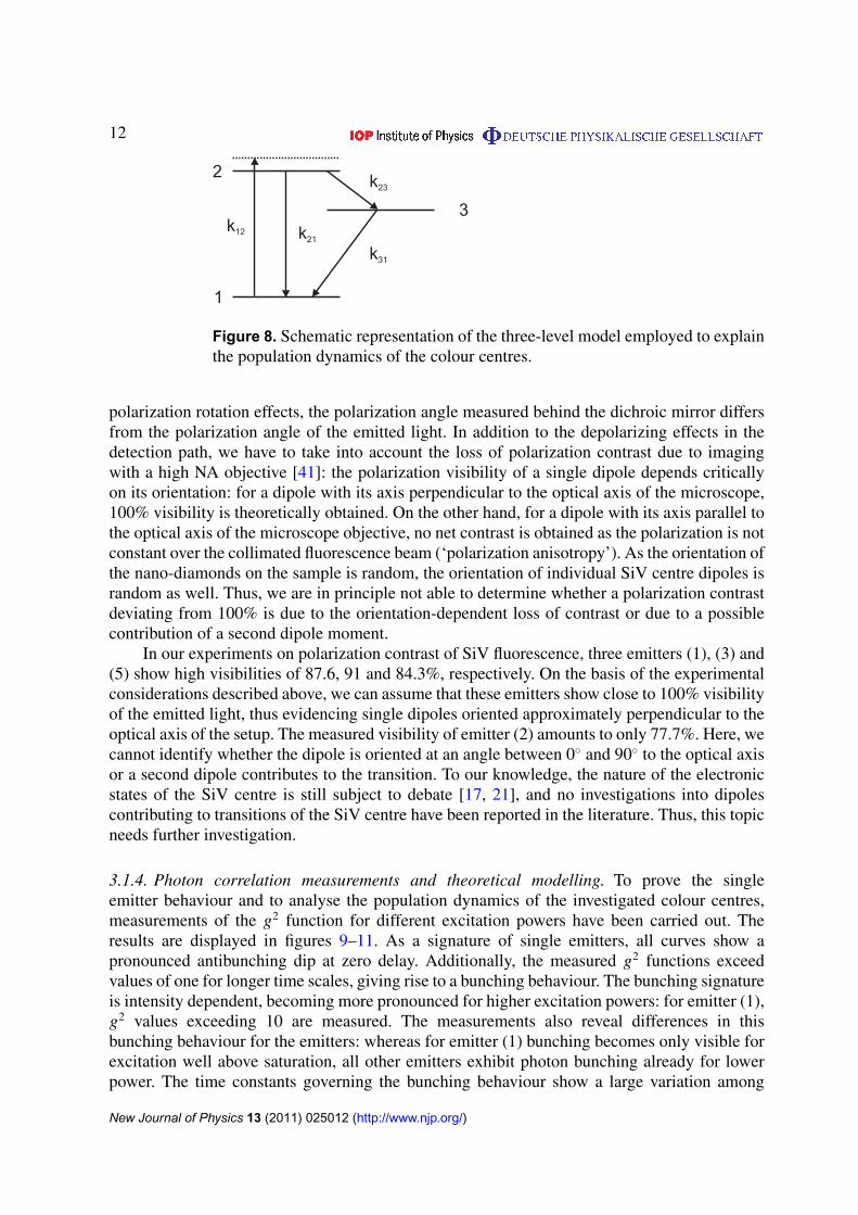
Figure 8. Schematic representation of the three-level model employed to explainthe population dynamics of the colour centres.
polarization rotation effects, the polarization angle measured behind the dichroic mirror differsfrom the polarization angle of the emitted light. In addition to the depolarizing effects in thedetection path, we have to take into account the loss of polarization contrast due to imagingwith a high NA objective [41]: the polarization visibility of a single dipole depends criticallyon its orientation: for a dipole with its axis perpendicular to the optical axis of the microscope,100% visibility is theoretically obtained. On the other hand, for a dipole with its axis parallel tothe optical axis of the microscope objective, no net contrast is obtained as the polarization is notconstant over the collimated fluorescence beam (‘polarization anisotropy’). As the orientation ofthe nano-diamonds on the sample is random, the orientation of individual SiV centre dipoles israndom as well. Thus, we are in principle not able to determine whether a polarization contrastdeviating from 100% is due to the orientation-dependent loss of contrast or due to a possiblecontribution of a second dipole moment.
In our experiments on polarization contrast of SiV fluorescence, three emitters (1), (3) and(5) show high visibilities of 87.6, 91 and 84.3%, respectively. On the basis of the experimentalconsiderations described above, we can assume that these emitters show close to 100% visibilityof the emitted light, thus evidencing single dipoles oriented approximately perpendicular to theoptical axis of the setup. The measured visibility of emitter (2) amounts to only 77.7%. Here, wecannot identify whether the dipole is oriented at an angle between 0◦ and 90◦ to the optical axisor a second dipole contributes to the transition. To our knowledge, the nature of the electronicstates of the SiV centre is still subject to debate [17, 21], and no investigations into dipolescontributing to transitions of the SiV centre have been reported in the literature. Thus, this topicneeds further investigation.
3.1.4. Photon correlation measurements and theoretical modelling. To prove the singleemitter behaviour and to analyse the population dynamics of the investigated colour centres,measurements of the g2 function for different excitation powers have been carried out. Theresults are displayed in figures 9–11. As a signature of single emitters, all curves show apronounced antibunching dip at zero delay. Additionally, the measured g2 functions exceedvalues of one for longer time scales, giving rise to a bunching behaviour. The bunching signatureis intensity dependent, becoming more pronounced for higher excitation powers: for emitter (1),g2 values exceeding 10 are measured. The measurements also reveal differences in thisbunching behaviour for the emitters: whereas for emitter (1) bunching becomes only visible forexcitation well above saturation, all other emitters exhibit photon bunching already for lowerpower. The time constants governing the bunching behaviour show a large variation among
New Journal of Physics 13 (2011) 025012 (http://www.njp.org/)

13
(a) (b)
Figure 9. Population dynamics of emitter (1). (a) The g2 functions for differentexcitation powers, given in units of the saturation power Psat = 14.3 µW. Forlower excitation power, the region of short delays is plotted (lower graph), whilefor higher powers, a larger region of delays is plotted, to permit observation ofthe bunching behaviour. Note that for low power, consecutive g2 functions havebeen displaced by 0.5 for clarity. Fits confirm that the residual g2(0) values aredue to the timing jitter only, unambiguously proving single emitter behaviour.(b) Constants τ1, τ2 and a obtained from the g2 functions. The constants τ2 forP < 125 µW are not given as they could not be reliably determined due to thevery low value of a.
the emitters: the g2 function of emitter (4) decays to a value of one for time delays of less than50 ns even at low power, whereas for emitters (1)–(3), time constants of more than 1 µs areobserved for low power, decreasing to below 100 ns for high excitation power.
To explain this behaviour, a three-level system including a ‘shelving state’ has to beconsidered. As the nature of the participating states is unknown, we use in a first approachthe simplified model depicted in figure 8: we assume that the excitation rate of level 2 dependslinearly on the excitation power P: k12 = σ P . Levels 1 and 2 are coupled via a fast radiativetransition with the rate coefficient k21, whereas level 3 acts as a ‘shelving state’ populated viathe rate coefficient k23 with the possibility of relaxation into the ground state via k31. As longas the emitter resides in state 3, no photons on the radiative transition 2 → 1 are detected. Thissimple model has been successfully employed to describe the dynamics of molecules involving
New Journal of Physics 13 (2011) 025012 (http://www.njp.org/)

14
(a) (b)
Figure 10. Population dynamics of emitter (3). (a) g2 functions for differentexcitation powers, given in units of the saturation power Psat = 40.9 µW. Forlower excitation power, the region of short delays is plotted (lower graph), whilefor higher powers a larger region of delays is plotted, to permit observation ofthe bunching behaviour. Note that for low power, consecutive g2 functions havebeen displaced by 0.5 for clarity. Fits confirm that the residual g2(0) values aredue to the timing jitter only, unambiguously proving single emitter behaviour.(b) Constants τ1, τ2 and a obtained from the g2 functions. Solid blue lines:intensity dependence obtained from the simple three-level model; dashed redlines: intensity dependence obtained from the extended model, including anintensity-dependent de-shelving.
shelving states [42]. Due to the very pronounced bunching behaviour at high powers, we excludeefficient power-dependent de-shelving processes, as described in [7, 11], and thus assume, in afirst approach, constant shelving and de-shelving rates k23 and k31, respectively. The g2 functiondescribes the dynamics and is defined by n2(τ )
n2(τ→∞), resulting in
g(2)(τ ) = 1 − (1 + a) e−|τ |/τ1 + a e−|τ |/τ2 . (3)
The parameters a, τ1 and τ2 are given by [33]
τ1,2 = 2/(A ±
√A2 − 4B), (4)
A = k12 + k21 + k23 + k31, (5)
New Journal of Physics 13 (2011) 025012 (http://www.njp.org/)

15
(a) (b)
Figure 11. g2 functions for emitters (2) and (4). (a) Power-dependent g2
functions for emitter (2). The inset displays the antibunching dip at 0.1Psat indetail. The fit confirms that the residual g2(0) is due to the timing jitter andthe short τ1 = 0.45 ns constant only, confirming single emitter behaviour. (b) g2
function of emitter (4) at P = 0.15Psat. The inset shows the antibunching dip indetail; again, the residual g2 is governed by the jitter only, confirming singleemitter behaviour with τ1 = 0.21 ns.
B = k12k23 + k12k31 + k21k31 + k23k31, (6)
a =1 − τ2k31
k31(τ2 − τ1). (7)
To describe the experimental results correctly, we have to account for the timing jitter ofthe APDs used. To this end, we convolute equation (3) with the measured Gaussian responsefunction of our setup (1/
√e width 354 ps). Figures 9–11 display the measured curves, including
the fits of equation (3) convoluted with the response function. The deviation from the expectedvalue g2(0) = 0 for a single emitter is fully explained by the timing jitter of the setup for lowexcitation power, thus unambiguously proving single emitter behaviour for the observed colourcentres. Note that no correction for background luminescence was necessary to obtain theseresults, confirming negligible background contributions. We note that this also holds for higherexcitation powers: for excitation powers of about Psat (emitters (1)–(3)), the deviation of thefitted g2(0) from the measured value is still only about 0.1. The results of the photon correlationmeasurements are thus consistent with values of g2(0)6 0.1.
The τ1 parameters at low excitation powers, indicating the lifetime of the excited stateunder the assumption k21 � k23 + k31, which is valid in our case, as shown later, show a largevariation from 2 ns for emitter (3) down to 0.2 ns for emitter (4). The variation of the observedexcited state lifetimes might be due to several reasons. Firstly, the SiV centre is assumed topossess a strong non-radiative decay channel [19]. This non-radiative decay channel varies withlocal strain in different nano-diamonds [20]. Secondly, the excited state lifetime is modified bythe presence of the metal layer. To estimate this influence, we perform three-dimensional finite-difference time domain calculations (FDTD Solutions, Lumerical). To simplify the problem,we assume an emitting dipole in a semi-infinite diamond slab (refractive index n = 2.4) above a
New Journal of Physics 13 (2011) 025012 (http://www.njp.org/)

16
Figure 12. Decay rates of an emitting dipole in diamond parallel to an iridiumlayer for different distances from the layer. The decay rates have been normalizedto the rates of the dipole embedded in diamond without the presence of theiridium layer.
semi-infinite iridium layer (ε = −18 + i · 25 at 740 nm [43]). As the orientation of the emittingdipole is unknown, we simulate a dipole parallel to the iridium layer as a first estimate. Theinfluence of the metal layer can be divided into two regimes: at distances & λ
2 (≈155 nm indiamond for the investigated colour centres), the lifetime usually shows an oscillatory behaviourdue to far-field interaction of the dipole with its mirror image [24]–[26]. We disregard thisregime as the diamond nano-crystals have a mean size of 130 nm and the emitter–metal distancethus is.130 nm. In figure 12, we present the results for the radiative and non-radiative as well asthe total decay rates for a dipole parallel to the iridium layer at distances between 10 and 70 nmfrom the iridium surface. Note that the rates are normalized with respect to the decay rates of anequivalent dipole in bulk diamond. At these distances, there is a strong influence of the metalas the dipole near-field components efficiently couple to evanescent waves in the metal. Themodification of the decay rates is especially pronounced for distances of less than 20 nm: dueto the near-field coupling to the absorbing metal, the non-radiative decay rate is enhanced bya factor of eight, while the radiative decay is simultaneously lowered by more than a factor oftwo. For a distance of 60 nm, the decay rates roughly match the rates for the dipole without thepresence of the iridium layer. Thus, the presence of the metal layer might account for a spreadof approximately a factor of eight in the measured lifetimes due to the varying positions of thecolour centres in the nano-diamonds. However, we note that the lifetime reduction does not leadto an enhanced radiative decay due to the quenching by the metal, in agreement with previousobservations [24].
The rate coefficients k12, k21, k23 and k31 governing the population dynamics of the colourcentres are derived from the limiting values of the fitted parameters a, τ1 and τ2,
k31 =1
(1 + a∞)τ∞
2
, (8)
k23 = k31a∞, (9)
k21 =1
τ 01
− k23 for k21 + k23 > k31, (10)
New Journal of Physics 13 (2011) 025012 (http://www.njp.org/)

17
where the superscript ∞ denotes the limit for high excitation power and 0 denotes the limit forvanishing excitation power. The values of a, τ1 and τ2 for emitters (1) and (3) are displayedin figures 9(b) and 10(b). The data indicate the limiting values of a, τ1 and τ2 despite the factthat some oscillatory behaviour is observed. This might be due to experimental reasons: abovesaturation, spatial drifts changing the intensity impinging on the emitter do no longer lead tomeasurable photon count rate changes, thus making the detection of drifts and ensuring constantexcitation intensity very challenging. Nevertheless, a rough estimate of the rate coefficients ispossible for emitters (1) and (3): we obtain k21 = 564 MHz, k23 = 1.4 MHz, k31 = 0.14 MHz foremitter (1) and k21 = 469 MHz, k23 = 6.7 MHz, k31 = 5.0 MHz for emitter (3). With these ratecoefficients and the measured saturation power Isat, we obtain the power dependence of a, τ1 andτ2 shown as solid lines in figures 9(b) and 10(b). The curves qualitatively resemble the observedbehaviour with deviations especially for τ2 and a at low powers.
In the following, we propose an extension of the simple three-level model in figure 8,allowing one to account for these deviations. For the discussion, we exemplarily use the dataobtained from emitter (3). As an alternative to the limiting values used in equation (8), we nowemploy the limiting value of τ2 for zero excitation,
k31 =1
τ 02
. (11)
By using equation (11) instead of (8) together with equations (9) and (10), we obtain an‘alternative’ set of rate parameters: k21 = 465 MHz, k23 = 11.3 MHz, k31 = 0.49 MHz. Thus, thevalue of k31 seems to be inconsistent for high and low excitation powers, indicating an intensity-dependent de-shelving process. As mentioned before, we exclude a de-shelving process linearlydependent on excitation power [7, 11, 44], as this model would lead to
τ∞
2 = 0, a∞= 0, (12)
which is not consistent with our observations. We therefore tentatively modify the intensitydependence of the rate k31 to follow a saturation law, including an intensity-independentrate k0
31,
k31 =d · P
P + c+ k0
31. (13)
The introduction of a saturating de-shelving process is further motivated by the possibleexplanation of this process as an excitation from the shelving state to higher-lying states, ase.g. found for molecules in [44]. This excitation process might intrinsically exhibit a saturationbehaviour. For the new model, we calculate k23, k21, k0
31 and d under the assumption k21 + k23 >
k031,
k031 =
1
τ 02
, (14)
d =1/τ∞
2 − (1 + a∞)/τ 02
a∞ + 1, (15)
k23 =1
τ∞
2
− k031 − d, (16)
k21 =1
τ 01
− k23. (17)
New Journal of Physics 13 (2011) 025012 (http://www.njp.org/)

18
For emitter (3), we obtain the following with equations (14)–(17) and a∞, τ 01 , τ 0
2 and τ∞
2derived from the measurements: k0
31 = 0.50 MHz, k23 = 6.72 MHz, k21 = 469.48 MHz and d =
4.55 MHz. Now the parameter c as well as the proportionality constant σ for the excitation ratek12 = σ P can be determined by fitting the intensity-dependent data for a with equation (7) (σ isno longer accessible from the saturation measurement in this model). The results are shown infigure 10(b); we obtain c = 98.1 µW and σ = 5.72 MHz µW−1. With these values of c and σ ,the intensity dependence of τ1 and τ2 is also well described. We thus conclude that a complexpower dependence of the de-shelving rate has to be accounted for to properly model the SiVcentre dynamics. To prove the general validity of this model, it has to be tested on a largernumber of emitters.
The rate coefficients determine the maximum obtainable photon count rate I∞ forcw excitation and the maximum steady-state population of the excited state n∞
2 = n2(τ →
∞, k12 → ∞),
I∞ = ηcoll ηqe k21 n∞
2 = ηcoll ηqek21
1 + (k23/(k031 + d))
. (18)
For the simple three-level model, k031 + d has to be replaced by the intensity-independent rate
k31. As the orientation of the emitting dipole inside the nano-crystal is unknown, the actualcollection efficiency ηcoll includes an uncertainty of a factor of 2.4, as discussed in section 3.1.2.In addition, the rate coefficients have to be considered as a rough estimate; thus, determiningthe quantum efficiency ηqe from the measured photon rate is not reliable. Nevertheless, by usingthe rate coefficients, we illustrate the influence of the shelving state on the maximum photoncount rate for cw excitation: for an off-resonantly pumped two-level system with decay rate k21,we expect a maximum photon rate,
I∞ = ηcoll ηqe k21n∞
2 = ηcoll ηqe k21. (19)
Thus, we deduce that for emitter (3) the presence of the shelving state changes the maximumphoton rate only by about a factor of two as n∞
2 = 0.43 compared to n∞
2 = 1 for an off-resonantlypumped two-level system. In contrast, for emitter (1), the presence of the shelving state leadsto n∞
2 = 0.09, thus potentially lowering the maximum photon rate by a factor of more than10. As the nature of the shelving state and the relaxation process is unknown, the reason forthe differences in bunching behaviour remains unclear. We emphasize that the large spread inexcited state lifetimes in combination with large differences in shelving state dynamics sufficesto explain large variations in photon emission rates of SiV centres.
3.2. Single emitter spectroscopy at cryogenic temperatures
Spectroscopy of colour centres at cryogenic temperatures is an important issue for theirapplication in quantum optics: underlying fine structures of ZPLs can only be observed atcryogenic temperatures reducing phonon broadening; additionally the determination of low-temperature line widths is crucial for applications involving coherent processes. We characterizeemitter (5) at room temperature and at 30 K. Figure 13 displays the measured spectra. Note thatg2 measurements prove single emitter behaviour for both temperatures. Emitter (5) has a roomtemperature line width of 1 nm. Upon cooling to 30 K, a fine structure evolves consisting offour components at 740.42 nm, 740.11 nm, 739.19 nm and 738.91 nm. The line width of theindividual components reduces to 0.17 nm. This four-line fine structure is characteristic of SiVcentres and has so far been observed only for ensembles of SiV centres in single crystals of high
New Journal of Physics 13 (2011) 025012 (http://www.njp.org/)

19
Figure 13. Temperature-dependent spectra of emitter (5). The spectra have beenmeasured at 290 K (red triangles) and 30 K (blue squares). The inset displays theg2 function of emitter (5) measured at 1.3 µW. The fit confirms that the residualg2(0) value is fully explained by the timing jitter of the setup, thus proving theexistence of a single emitter.
quality [17, 22], thus providing significant evidence for the identification of the observed colourcentres as SiV centres. The spacing of the outer components is 1.5 nm. For SiV centres in singlecrystals this spacing increases from 0.7 nm (no stress) to 2.4 nm by applying a stress of 0.5 GPaalong the (001) direction [22]. Thus, the observed spacing can be explained by stress insidethe nano-crystal. The spectrum shifts by 1.5 nm to shorter wavelengths when cooling to 30 K(highest fine structure peak compared to room temperature ZPL). This shift is also characteristicof SiV centres in poly-crystalline CVD diamonds: Ghorokovsky et al [32] as well as Feng andSchwartz [20] observed a blue shift of 1.4 and 1.2 nm, respectively, when cooling to 100 K andno further shift for lower temperatures. For the observed single SiV centre, the line shifting alsostops around 110 K, thus resembling the observations for ensembles.
4. Conclusion
We have identified an advanced material system for single photon sources in diamondemploying high-quality CVD nano-diamonds on iridium produced via spin coating seedingand microwave CVD growth. Due to impurities in the growth process, single SiV centresare formed. The iridium substrates together with the small-volume nano-diamonds provide amajor advantage, namely single photon emission with negligible contributions of backgroundfluorescence. Furthermore, the SiV colour centres observed here are much better than theirreputation and exhibit very promising behaviour as single photon sources: line widths aslow as 0.7 nm could be detected with a fraction of up to 88% of photons emitted into theZPL. In addition, the observed colour centres feature count rates up to 4.8 Mcps, thus beingthe brightest diamond-based single photon sources to date. By performing spectroscopy atcryogenic temperatures, we verify the identification of these colour centres as SiV centres,measuring for the first time the fine structure splitting of a single SiV centre.
New Journal of Physics 13 (2011) 025012 (http://www.njp.org/)

20
Acknowledgments
SEM analysis of the samples was performed by J Schmauch (Universität des Saarlandes,Saarbrücken, Germany) and M Fischer (Universität Augsburg, Germany). We thank L Marquantfor help with the spin-coating procedure and R Albrecht (Universität des Saarlandes,Saarbrücken, Germany) for valuable help. The SiV structure in figure 1(a) was drawn by C Hepp(Universität des Saarlandes, Saarbrücken, Germany); B Weigand (Universität des Saarlandes,Saarbrücken, Germany) assisted with the g2 fitting procedure. This work was financiallysupported by the Deutsche Forschungsgemeinschaft and the Bundesministerium für Bildungund Forschung (the network EphQuaM, contract no. 01BL0903).
References
[1] Gisin N, Ribordy G, Tittel W and Zbinden H 2002 Rev. Mod. Phys. 74 145[2] Kurtsiefer C, Mayer S, Zarda P and Weinfurter H 2000 Phys. Rev. Lett. 85 290[3] Rabeau J, Stacey A, Rabeau A, Prawer S, Jelezko F, Mirza I and Wrachtrup J 2007 Nano Lett. 7 3433[4] Beveratos A, Brouri R, Gacoin T, Poizat J and Grangier P 2001 Phys. Rev. A 64 61802[5] Wu E, Rabeau J R, Roger G, Treussart F, Zeng H, Grangier P, Prawer S and Roch J F 2007 New J. Phys.
9 434[6] Gaebel T, Popa I, Gruber A, Domham M, Jelezko F and Wachtrup J 2004 New J. Phys. 6 98[7] Wu E, Jacques V, Zeng H, Grangier P, Treussart F and Roch J R 2006 Opt. Express 14 1296[8] Rabeau J, Chin Y, Prawer S, Jelezko F, Gaebel T and Wrachtrup J 2005 Appl. Phys. Lett. 86 131926[9] Steinmetz D, Neu E, Hepp C, Albrecht R, Bolse W, Meijer J, Rogalla D and Becher C 2010 Proc. SPIE
7727 77270P[10] Aharonovich I, Zhou C, Stacey A, Orwa J, Castelletto S, Simpson D, Greentree A, Treussart F, Roch J F and
Prawer S 2009 Phys. Rev. B 79 235316[11] Aharonovich I, Castelletto S, Simpson D A, Greentree A D and Prawer S 2010 Phys. Rev. A 81 043813[12] Aharonovich I, Castelletto S, Johnson B C, McCallum J C, Simpson D A, Greentree A D and Prawer S 2010
Phys. Rev. B 81 121201[13] Wang C, Kurtsiefer C, Weinfurter H and Burchard B 2006 J. Phys. B: At. Mol. Opt. 39 37[14] Jelezko F, Gaebel T, Popa I, Gruber A and Wrachtrup J 2004 Phys. Rev. Lett. 93 130501[15] Neumann P et al 2010 Nat. Phys. 6 249[16] Iakoubovskii K and Adriaenssens G 2000 Diam. Relat. Mater. 9 1349[17] Clark C D, Kanda H, Kiflawi I and Sittas G 1995 Phys. Rev. B 51 16681[18] Zaitsev A 2001 Optical Properties of Diamond: A Data Handbook (Berlin: Springer)[19] Turukhin A V, Liu C H, Gorokhovsky A A, Alfano R R and Phillips W 1996 Phys. Rev. B 54 16448[20] Feng T and Schwartz B 1993 J. Appl. Phys. 73 1415[21] Goss J P, Jones R, Breuer S J, Briddon P R and Öberg S 1996 Phys. Rev. Lett. 77 3041[22] Sternschulte H, Thonke K, Sauer R, Münzinger P C and Michler P 1994 Phys. Rev. B 50 14554[23] Babinec T et al 2010 Nat. Nanotechnol. 5 195[24] Buchler B, Kalkbrenner T, Hettich C and Sandoghdar V 2005 Phys. Rev. Lett. 95 063003[25] Lukosz W and Kunz R 1977 J. Opt. Soc. Am. 67 1607[26] Vion C, Spinicelli P, Coolen L, Schwob C, Frigerio J M, Hermier J P and Maitre A 2010 Opt. Express
18 7440[27] Gsell S, Bauer T, Goldfuß J, Schreck M and Stritzker B 2004 Appl. Phys. Lett. 84 4541[28] Ruan J, Choyke W and Kobashi K 1993 Appl. Phys. Lett. 62 1379[29] Stacey A, Aharonovich I, Prawer S and Butler J 2009 Diam. Relat. Mater. 18 51[30] Bergman L, Stoner B, Turner K, Glass J and Nemanich R 1993 J. Appl. Phys. 73 3951
New Journal of Physics 13 (2011) 025012 (http://www.njp.org/)

21
[31] Fischer M, Brescia R, Gsell S, Schreck M, Brugger T, Greber T, Osterwalder J and Stritzker B 2008 J. Appl.Phys. 104 123531
[32] Gorokhovsky A, Turukhin A, Alfano R and Phillips W 1995 Appl. Phys. Lett. 66 43[33] Wang C 2007 A solid-state single photon source based on color centers in diamond PhD Thesis Technische
Universität, München[34] Davies G 1981 Rep. Prog. Phys. 44 787[35] Walker J 1979 Rep. Prog. Phys. 42 1605[36] Sittas G, Kiflawi I, Kanda H and Spear P 1996 Diam. Relat. Mater. 5 866[37] Plakhotnik T, Moerner W, Palm V and Wild U 1995 Opt. Commun. 114 83[38] Fu K M C, Santori C, Barclay P E and Beausoleil R G 2010 Appl. Phys. Lett. 96 121907[39] Ha T, Laurence T, Chemla D and Weiss S 1999 J. Phys. Chem. B 103 6839[40] Alegre T P M, Santori C, Medeiros-Ribeiro G and Beausoleil R G 2007 Phys. Rev. B 76 165205[41] Fourkas J 2001 Opt. Lett. 26 211[42] Kitson S, Jonsson P, Rarity J and Tapster P 1998 Phys. Rev. A 58 620[43] Weaver J H, Olson C G and Lynch D W 1977 Phys. Rev. B 15 4115[44] Fleury L, Segura J, Zumofen G, Hecht B and Wild U 2000 Phys. Rev. Lett. 84 1148
New Journal of Physics 13 (2011) 025012 (http://www.njp.org/)