single palladium nanowires that resist fracture...
TRANSCRIPT
Subscriber access provided by - Access paid by the | UC Irvine Libraries
Nano Letters is published by the American Chemical Society. 1155 SixteenthStreet N.W., Washington, DC 20036
Letter
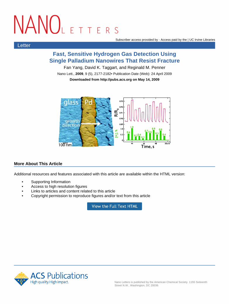
Fast, Sensitive Hydrogen Gas Detection UsingSingle Palladium Nanowires That Resist Fracture
Fan Yang, David K. Taggart, and Reginald M. PennerNano Lett., 2009, 9 (5), 2177-2182• Publication Date (Web): 24 April 2009
Downloaded from http://pubs.acs.org on May 14, 2009
More About This Article
Additional resources and features associated with this article are available within the HTML version:
• Supporting Information• Access to high resolution figures• Links to articles and content related to this article• Copyright permission to reproduce figures and/or text from this article
Fast, Sensitive Hydrogen Gas DetectionUsing Single Palladium Nanowires ThatResist FractureFan Yang, David K. Taggart, and Reginald M. Penner*
Department of Chemistry, UniVersity of California, IrVine, California 92697-2025
Received March 16, 2009; Revised Manuscript Received April 13, 2009
ABSTRACT
Two types of pure palladium (Pd) nanowires, differentiated by microstructure, were electrodeposited: (1) nanocrystalline Pd nanowires (graindiameter ≈ 5 nm, henceforth nc5-Pd) and (2) nanocrystalline Pd nanowires with a grain diameter of 15 nm (nc15-Pd). These nanowires wereevaluated for the detection of hydrogen gas (H2). Despite their fundamental similarities, the behavior of these nanowires upon exposure to H2
was dramatically and reproducibly different: nc5-Pd nanowires spontaneously fractured upon exposure to H2 above 1-2%. Fractured nanowirescontinued to function as sensors for H2 concentrations above 2%, actuated by the volume change associated with the r to phase transitionof PdHx. nc15-Pd nanowires, in contrast, withstood repeated exposures to H2 up to 10% without fracturing. nc15-Pd nanowires showed a rapid(2 s at 10%) increase in resistance in the presence of H2 and a response that scaled smoothly with [H2] spanning 5 orders of magnitude downto 2 ppm.
Hydrogen (H2) gas sensors that are sensitive, rapid-respond-ing, stable, compact, and inexpensive are needed to optimizethe performance and ensure the safety of devices like fuelcells that are powered by H2. Palladium (Pd) nanowires areattractive candidates for H2 sensors because they are able toequilibrate rapidly with H2, leading to a rapid response time.Palladium absorbs hydrogen to form a hydride (PdHx) withx saturating at 0.67,1,2 and since 1869 it has been knownthat the electrical resistivity of this hydride increases linearlywith x by a factor of 1.8-1.9 over the range from x ) 0 to0.67.1 This property of PdHx was first exploited for hydrogensensing by Hughes and Schubert 1992.3 As hydrogen gassensors, Pd resistors are elegant in their simplicity but theyhave several deficiencies: (1) Hydrogen atom diffusion inpalladium is slow at room temperature (DH ) 3.8 × 10⁻⁷
cm2/s at 298 K).1,2 This means that the Pd resistor must beheated to 70 °C or higher to activate diffusion degradingthe power efficiency of the device. (2) The R to phasetransition of PdHx, occurring over the range from 1 to 2%H2 (in this paper we refer exclusively to the volumetricpercentage, v/v %), mechanically stresses the resistor causingdeformation and delamination while simultaneously retardingthe sensor response time. (3) hydrogen sulfide, ammonia,water, and hydrocarbons interfere with H2 detection at Pdbecause they dissociatively chemisorb, often irreversibly, toproduce adsorbed hydrogen atoms and block the adsorptionof dihydrogen.
By reducing the distance over which hydrogen mustdiffuse within the palladium sensing element, the retarding
effect of slow proton diffusion on the response time of theresistor is minimized. This was the rational for exploringthe use of palladium nanowires in hydrogen sensors in 2001.4
These early sensors4,5 consisted of ensembles of hundredsof Pd nanowires, 150-300 nm in diameter. Exposure of thesenanowires to H2 at concentrations above 2% caused eachnanowire to fracture approximately every 2 µm along its axisresulting in a loss of electrical continuity. Subsequentexposures to H2 above the 1-2% threshold for the R to phase transition swelled the nanowire and closed thesefractures, restoring electrical continuity. These sensors hada rapid response time of <1 s, but the limit-of-detection(LODH2
) was in the 2% range necessary to induce the R to phase transition. This LODH2
is too high even for H2 leakdetection since the lower explosion limit for H2 of 4% isjust incrementally higher.
Since 2002, palladium nanostructures have been used ina variety of innovative ways as resistor-based hydrogensensors. These sensors can be categorized according to themechanism by which they transduce hydrogen: Sensors thatderive their signal from the volume change associated withthe R to phase transition generally show decreasedresistance in the presence of hydrogen (i.e., ∆RH2
(-)) whilethose that measure the increased resistance of the PdHx
relative to Pd show an increased resistance upon H2 exposure(i.e., ∆RH2
(+)). Two-dimensional palladium nanoparticulatefilms6-11 fall into the first category. An attribute of thesesystems is that they often have rapid response times (<1s)that mimic the early palladium nanowire arrays,4,5 and they
NANOLETTERS
2009Vol. 9, No. 52177-2182
10.1021/nl9008474 CCC: $40.75 2009 American Chemical SocietyPublished on Web 04/24/2009
are much easier to fabricate. Yun and co-workers12 elec-trodeposited single palladium nanowires and showed thatthese function as H2 sensors in this ∆RH2
(-) mode. A∆RH2
(-) sensor was also produced by using a focused ionbeam to cut a nanotrench with width 100-400 nm into apalladium microwire.13 With a few exceptions,8,14 ∆RH2
(-)sensors show a LODH2
in the 1-2% range coinciding withthe threshold for the R to phase transition. A lower LODH2
can be obtained for systems capable of functioning in the∆RH2
(+) regime because the increased resistance of PdHx
can be detected well below the 1-2% threshold for the R to phase transition, often at the expense of slower sensorresponse and recovery times. Myung and co-workers15
recently showed that a sensitive ∆RH2(+) hydrogen sensor
is obtained when carbon nanotubes arrayed between twoelectrical contacts are electrochemically decorated withpalladium nanoparticles. These sensors showed a LODH2
of100 ppm with response times in the 5-10 min range. Wedemonstrate below that by controlling the grain structure ofa palladium nanowire, nanowires operating in either the∆RH2
(+) or the ∆RH2(-) modes can be obtained. But
superior H2 sensing performance, including response timesin the 1-5 s range at high H2 concentrations and a LODH2
of 2 ppm, are demonstrated for single Pd nanowire sensorsoperating in the ∆RH2
(+) mode that did not break uponexposure to H2.
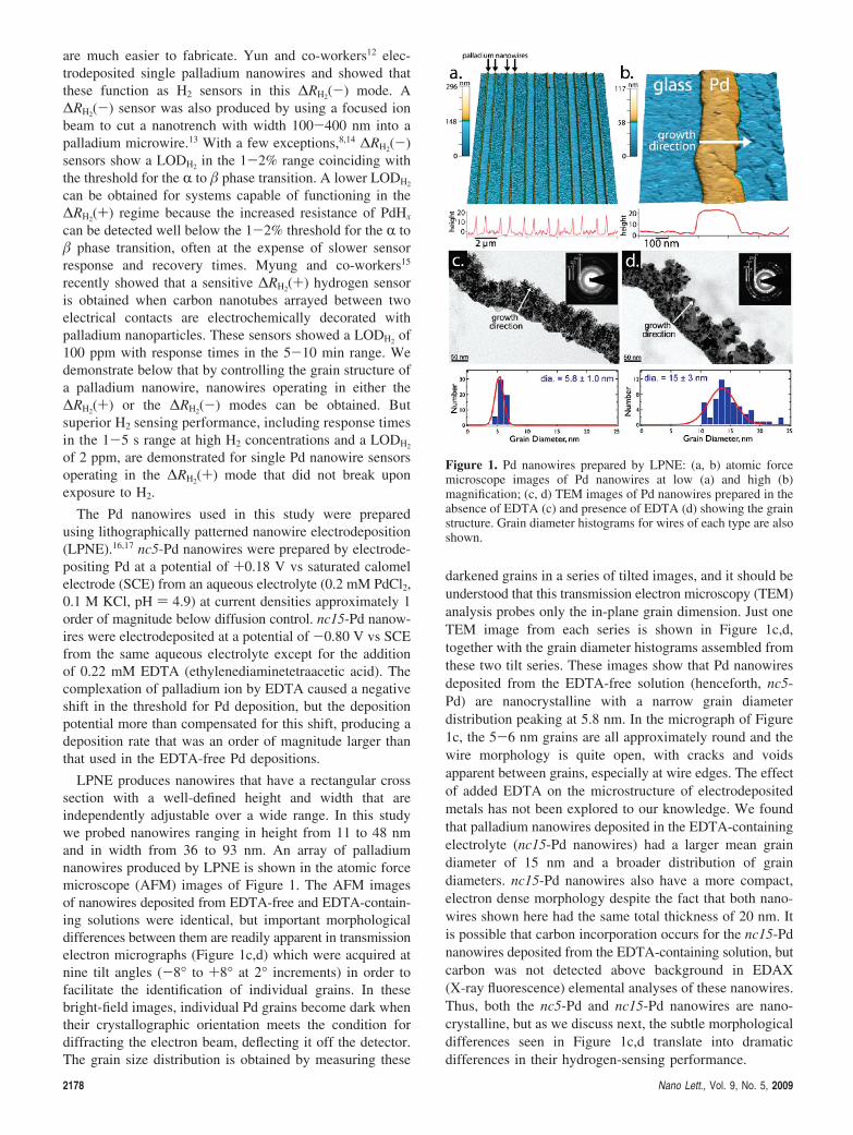
The Pd nanowires used in this study were preparedusing lithographically patterned nanowire electrodeposition(LPNE).16,17 nc5-Pd nanowires were prepared by electrode-positing Pd at a potential of +0.18 V vs saturated calomelelectrode (SCE) from an aqueous electrolyte (0.2 mM PdCl2,0.1 M KCl, pH ) 4.9) at current densities approximately 1order of magnitude below diffusion control. nc15-Pd nanow-ires were electrodeposited at a potential of -0.80 V vs SCEfrom the same aqueous electrolyte except for the additionof 0.22 mM EDTA (ethylenediaminetetraacetic acid). Thecomplexation of palladium ion by EDTA caused a negativeshift in the threshold for Pd deposition, but the depositionpotential more than compensated for this shift, producing adeposition rate that was an order of magnitude larger thanthat used in the EDTA-free Pd depositions.
LPNE produces nanowires that have a rectangular crosssection with a well-defined height and width that areindependently adjustable over a wide range. In this studywe probed nanowires ranging in height from 11 to 48 nmand in width from 36 to 93 nm. An array of palladiumnanowires produced by LPNE is shown in the atomic forcemicroscope (AFM) images of Figure 1. The AFM imagesof nanowires deposited from EDTA-free and EDTA-contain-ing solutions were identical, but important morphologicaldifferences between them are readily apparent in transmissionelectron micrographs (Figure 1c,d) which were acquired atnine tilt angles (-8° to +8° at 2° increments) in order tofacilitate the identification of individual grains. In thesebright-field images, individual Pd grains become dark whentheir crystallographic orientation meets the condition fordiffracting the electron beam, deflecting it off the detector.The grain size distribution is obtained by measuring these
darkened grains in a series of tilted images, and it should beunderstood that this transmission electron microscopy (TEM)analysis probes only the in-plane grain dimension. Just oneTEM image from each series is shown in Figure 1c,d,together with the grain diameter histograms assembled fromthese two tilt series. These images show that Pd nanowiresdeposited from the EDTA-free solution (henceforth, nc5-Pd) are nanocrystalline with a narrow grain diameterdistribution peaking at 5.8 nm. In the micrograph of Figure1c, the 5-6 nm grains are all approximately round and thewire morphology is quite open, with cracks and voidsapparent between grains, especially at wire edges. The effectof added EDTA on the microstructure of electrodepositedmetals has not been explored to our knowledge. We foundthat palladium nanowires deposited in the EDTA-containingelectrolyte (nc15-Pd nanowires) had a larger mean graindiameter of 15 nm and a broader distribution of graindiameters. nc15-Pd nanowires also have a more compact,electron dense morphology despite the fact that both nano-wires shown here had the same total thickness of 20 nm. Itis possible that carbon incorporation occurs for the nc15-Pdnanowires deposited from the EDTA-containing solution, butcarbon was not detected above background in EDAX(X-ray fluorescence) elemental analyses of these nanowires.Thus, both the nc5-Pd and nc15-Pd nanowires are nano-crystalline, but as we discuss next, the subtle morphologicaldifferences seen in Figure 1c,d translate into dramaticdifferences in their hydrogen-sensing performance.
Figure 1. Pd nanowires prepared by LPNE: (a, b) atomic forcemicroscope images of Pd nanowires at low (a) and high (b)magnification; (c, d) TEM images of Pd nanowires prepared in theabsence of EDTA (c) and presence of EDTA (d) showing the grainstructure. Grain diameter histograms for wires of each type are alsoshown.
2178 Nano Lett., Vol. 9, No. 5, 2009

From a purely electrical standpoint, nc15-Pd nanowiresand nc5-Pd nanowires were similar: nc15-Pd nanowireselectrodeposited from EDTA-containing solutions had elec-trical resistivities that were ≈30% lower than those obtained
for nc5-Pd nanowires of closely matched height andwidthsqualitatively as expected and as reported previouslyfor other metals, such as copper.18,19 These resistance valuesare 20-50 times higher than those for bulk palladium.17
Hydrogen sensors were fabricated from single Pd nano-wires supported on glass by evaporating gold electricalcontacts (Figure 2a) and attaching copper wires to thesecontacts using silver paint. These evaporated contacts isolateda 100 µm length of each nanowire (Figure 2b) and theelectrical resistance of this wire section was measured usingfour electrical contacts as a function of time during theexposure of the sensor to pulses of hydrogen of predeter-mined concentrationsdetermined by mixing of H2 and N2
flowstreamsatflowratesdeterminedbymassflowcontrollerssin a flowing stream of pure nitrogen gas.
A plot of resistance versus time for the exposure of a singlenc5-Pd nanowire to a series of hydrogen pulses near 1% isshown in Figure 3a. An increase in the wire resistance (∆R/R0 ≈ 15%) is seen during each hydrogen exposure for thefirst five of these pulses and then, during the sixth pulse, theresistance increases to more than 10 MΩ. This rapid increasein resistance signals the formation of fractures in the Pdnanowire. After fracturing, the nc5-Pd nanowire shows nodetectible response to H2 exposure below 1%, but for higherconcentrations, the nanowire resistance rapidly and reversiblydecreases and the amplitude of this resistance change, plottedas an increased conductance in Figure 3c, correlates with
Figure 2. Pd nanowire-based H2 sensors. (a-c) Scanning electron microscope images at progressively higher magnification of a H2 sensorconsisting of a single Pd nanowire with evaporated four-contact electrodes.
Figure 3. Fracture of nc5-Pd nanowire upon H2 exposure. (a) Plotsof resistance versus time during the exposure of a single 40 × 430nm Pd nanowire to pulses of 1.2%-2.0% hydrogen as indicatedby the program at bottom. Fracture of the nanowire on the sixthexposure is signaled by an increase in the resistance to >10 M Ω.(b) Calibration plot for the response of a fractured nc5-Pd nanowireto H2. Error bars indicate (1 standard deviation of the mean formultiple trials. (c) Conductance versus time for the exposure of afractured nc5-Pd nanowire to pulses of hydrogen ranging inconcentration from 0.5% to 7% (d-f) Scanning electron microscopeimages at low magnification (d) and higher magnification (e, f)showing fractures produced by H2 exposure.
Figure 4. Initial exposures of a 20 × 42 nm nc15-Pd nanowire toH2. (a) R/R0 versus time for the exposure to 77 pulses of H2 rangingin concentration from 0.2% to 1.0%. (b) R/R0 versus time for thefinal sequence of 11 H2 exposures comparing the applied concentra-tion program (bottom) with the observed nanowire response (top).
Nano Lett., Vol. 9, No. 5, 2009 2179
the [H2] over a narrow concentration range from 1 to 5%.For [H2] above 5%, no change in conductance is seen overthat measured at 5%. Over this 1-5% range, the reproduc-ibility of the conductance change is 10-20% (Figure 3b).These response characteristics are, in all respects, similar tothose reported for other ∆RH2
(-) sensors that transduce H2
using the R to phase transition of PdHx.4-11,13
That fracturing of the nc5-Pd nanowires has occurred isconfirmed by SEM examination of nc5-Pd nanowire afterexposure to H2 (Figure 3d). These nanowires are fracturedperiodically, every 10 µm, along the nanowire length witheach fracture defined by a 200-400 nm gap. The integratedgap length along each fractured nanowire corresponds to
3-4%, approaching the expected 3.5% linear expansioninduced by the R to phase transition of PdHx.1 Previously,4,5
we studied the properties of ensembles of 200 nm diameterPd nanowires for sensing hydrogen and we observed exactlythe same fracturing behavior in response to hydrogenexposure for these much larger nanowires. In 13 trialsinvolving the exposure of nc5-Pd nanowires to hydrogen inthe concentration range near 1%, all 13 nanowire fracturedin the manner depicted in Figure 3. We conclude that thesensing mechanism for fractured nc5-Pd nanowires involvesthe mechanical closing of these fractures upon exposure toH2 above 1% caused by the R to phase transition of PdHx
and the simultaneous swelling by 3.5% of the PdHx wire’s
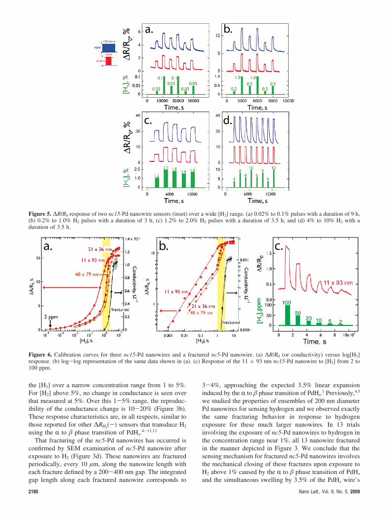
Figure 5. ∆R/R0 response of two nc15-Pd nanowire sensors (inset) over a wide [H2] range. (a) 0.02% to 0.1% pulses with a duration of 9 h,(b) 0.2% to 1.0% H2 pulses with a duration of 3 h, (c) 1.2% to 2.0% H2 pulses with a duration of 3.5 h, and (d) 4% to 10% H2 with aduration of 3.5 h.
Figure 6. Calibration curves for three nc15-Pd nanowires and a fractured nc5-Pd nanowire. (a) ∆R/R0 (or conductivity) versus log[H2]response. (b) log-log representation of the same data shown in (a). (c) Response of the 11 × 93 nm nc15-Pd nanowire to [H2] from 2 to100 ppm.
2180 Nano Lett., Vol. 9, No. 5, 2009
linear dimensions relative to Pd. A suspended wire in tensionshould fracture once, not multiple times, so the existence ofmultiple fractures (also as seen previously)4,5 requiresmultiple strong points of attachment between the wire andthe glass surfacesa minimum of one per fracturesarrayedalong each nanowire.
nc15-Pd nanowires did not fracture upon exposure tohydrogen at any concentration, and this fact permits thesenanowires to operate in the ∆RH2
(+) mode, enabling farsuperior H2 sensing performance as compared with nc5-Pdnanowires. The resistance of a freshly prepared nc15-Pdnanowire is shown in Figure 4a as it is repeatedly exposedto a sequence of H2 pulses ranging in concentration from0.2 to 1.0% over 14 h. Significant drift of the baselineresistance is seen in these data, but the drift decreasesprogressively over the 14 h experiment until at its conclusion,
it is reduced to ∆R/R0 ≈ 0.09%/hour. We preconditionedeach nc15-Pd nanowire employed for sensing to stabilizeits baseline resistance using this procedure.
Raw sensing data for two different nc15-Pd nanowires(Figure 5) show rapid, reversible increases in resistance for[H2] ranging from 0.02% to 10%. But the signal-to-noiseseen in Figure 5a at the lower end of this range supports thedetection of much lower H2, down to 2 ppm (Figure 6c).Calibration plots for nanowires of different widths andheights (Figure 6a,b) show very clearly the extendedconcentration range over which the nc15-Pd nanowires areable to operate relative to the nc5-Pd nanowires (labeled“fractured”). Less obvious, but of equal importance, is atremendous improvement in the reproducibility of the ∆R/R0 seen at each concentration which is reflected by the errorbars in each data set. These calibration plots also reveal that∆R/R0 is insensitive to the cross-sectional wire dimensions,and its initial resistance, to first order. For example, theelectrical resistance of the smaller nanowire (21 × 36 nm)was 305 kΩ and that of the larger nanowire (48 × 79 nm)was 40.8 kΩ, but these two nanowires produced the same∆R/R0, to within 5% over the entire concentration range from[H2] ) 0.02 to 10%.
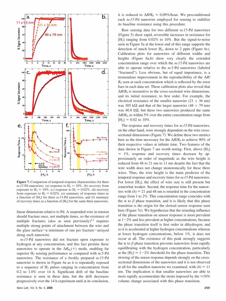
The response and recovery times for nc15-Pd nanowires,on the other hand, were strongly dependent on the wire cross-sectional dimensions (Figure 7). We define these two metricshere as the time necessary for the ∆R/R0 to achieve 90% oftheir respective values at infinite time. Two features of thedata shown in Figure 7 are worth noting: First, above [H2]) 1%, response and recovery times decrease by ap-proximately an order of magnitude as the wire height isreduced from 48 to 21 nm to 11 nm despite the fact that thewire width does not change monotonically for these threewires. Thus, the wire height is the main predictor of thetemporal response and recovery times for nc15-Pd nanowires.For lower [H2], the effect of wire size is still present butsomewhat weaker. Second, the response time for the nanow-ires with (h) ) 21 and 48 nm is retarded in the concentrationrange from 1 to 2%. This concentration range coincides withthe R to phase transition, and it is likely that this phasetransition is the origin for the slowed sensor response seenhere (Figure 7e). We hypothesize that the retarding influenceof the phase transition on sensor response is most prevalentat 1-2% and less prevalent at higher concentrations, becausethe phase transition itself is first order in dihydrogen, andso it is accelerated at higher hydrogen concentrations whereasat lower hydrogen concentrations, below 1%, it does notoccur at all. The existence of this peak strongly suggeststhe R to phase transition prevents nanowires from rapidlyequilibrating with the hydrogen concentration, particularlyat the [H2] ) 1-2% threshold for the phase transition. Thisslowing of the sensor response depends strongly on the cross-sectional dimensions of the nanowires and it is not observedat all for the smallest nanowire we examined, with (h) ) 11nm. The implication is that smaller nanowires are able tomore rapidly accommodate the strain imposed by the ≈10%volume change associated with this phase transition.
Figure 7. Comparison of temporal response characteristics for threenc15-Pd nanowires: (a) response to H2 ) 10%, (b) recovery fromexposure to H2 ) 10%, (c) response to H2 ) 0.02%, (d) recoveryfrom exposure to H2 ) 0.02%, (e) summary of response times asa function of [H2] for three nc15-Pd nanowires, and (f) summaryof recovery times as a function of [H2] for the same three nanowires.
Nano Lett., Vol. 9, No. 5, 2009 2181
The origin of the disparate mechanical behavior of the nc5-Pd nanowires and the nc15-Pd nanowires we have examinedhere is not addressed by our data. The canonical behaviorfor polycrystalline metals is increasing yield-strength, σy, witha reduction in the grain diameter, d, according to theHall-Petch equation20,21
σy ) σ0 +ky
√d(1)
where σ0 is a materials constant for the starting stress fordislocation movement and ky is the strengthening coefficient.In the sub-100-nm grain size regime that applies in this study,inVerse Hall-Petch behavior characterized by weakeningyield strength with reduction of the grain size has also beenreported.22 To date there have been no investigations of thetensile stress-strain behavior of polycrystalline nanowiresto our knowledge, but these data highlight the importanceof these investigations, and we are working to carry themout in our laboratory.
In summary, the effect of grain structure on the functionalproperties of polycrystalline nanowires has not been exam-ined in any context, to our knowledge. Here we havedemonstrated that for nanowires of pure palladium a subtledifference in grain structure is associated with disparate wirebehavior upon exposure to hydrogen gas leading to radicallyaltered functionality in the application of these nanowiresas hydrogen sensors. Specifically, single nc15-Pd nanowiresprepared from EDTA-containing plating solution are notsubject to fracturing when exposed to hydrogen and, for thisreason, they are able to rapidly and reversibly detecthydrogen as a resistance increase down to 2 ppm withexcellent reproducibility and baseline stability at roomtemperature.
Acknowledgment. This work was supported by NationalScience Foundation Grant CHE-0641169, the Petroleum
Research Fund of the American Chemical Society 46815-AC 10, and the UCI School of Physical Sciences Center forSolar Energy.
References(1) Lewis, F. A. The palladium hydrogen system; Academic Press: London,
1967.(2) Flanagan, T. B.; Oates, W. A. The palladium-hydrogen system; Annual
Reviews, Inc.: Palo Alto, CA1991; Vol. 21, pp 269-304.(3) Hughes, R. C.; Schubert, W. K. J. Appl. Phys. 1992, 71, 542–544.(4) Favier, F.; Walter, E.; Zach, M.; Benter, T.; Penner, R. Science 2001,
293, 2227–2231.(5) Walter, E.; Favier, F.; Penner, R. Anal. Chem. 2002, 74, 1546–1553.(6) Dankert, O.; Pundt, A. Appl. Phys. Lett. 2002, 81, 1618–1620.(7) Kaltenpoth, G.; Schnabel, P.; Menke, E.; Walter, E.; Grunze, M.;
Penner, R. Anal. Chem. 2003, 75, 4756–4765.(8) Xu, T.; Zach, M.; Xiao, Z.; Rosenmann, D.; Welp, U.; Kwok, W.;
Crabtree, G. Appl. Phys. Lett. 2005, 86, 203104.(9) Luongo, K.; Sine, A.; Bhansali, S. Sens. Actuators, B 2005, 111, 125–
129.(10) Khanuja, M.; Varandani, D.; Mehta, B. R. Appl. Phys. Lett. 2007, 91,
253121.(11) Ibanez, F. J.; Zamborini, F. P. J. Am. Chem. Soc. 2008, 130, 622–
633.(12) Im, Y.; Lee, C.; Vasquez, R.; Bangar, M.; Myung, N.; Menke, E.;
Penner, R.; Yun, M. Small 2006, 2, 356–358.(13) Kiefer, T.; Favier, F.; Vazquez-Mena, O.; Villanueva, G.; Brugger, J.
Nanotechnology 2008, 19, 125502.(14) Kim, K.; Sim, S.; Cho, S. IEEE Sens. J. 2006, 6, 509–513.(15) Mubeen, S.; Zhang, T.; Yoo, B.; Deshusses, M. A.; Myung, N. V. J.
Phys. Chem. C 2007, 111, 6321–6327.(16) Menke, E. J.; Thompson, M. A.; Xiang, C.; Yang, L. C.; Penner, R. M.
Nat. Mater. 2006, 5, 914–919.(17) Xiang, C.; Kung, S. C.; Taggart, D.; Yang, F.; Thompson, M. A.;
Guell, A. G.; Yang, Y.; Penner, R. M. ACS Nano 2008, 2, 1939–1949.
(18) Steinhogl, W.; Schindler, G.; Steinlesberger, G.; Engelhardt, M. Phys.ReV. B 2002, 66, 075414.
(19) Steinhogl, W.; Schindler, G.; Steinlesberger, G.; Traving, M.; Engel-hardt, M. J. Appl. Phys. 2005, 97, 023706.
(20) Petch, N. J. Iron Steel Inst., London 1953, 25–28.(21) Hall, E. Phys. Soc., Ser. B 1951, 64, 747–753.(22) Carlton, C. E.; Ferreira, P. J. Acta Mater. 2007, 55, 3749–3756.
NL9008474
2182 Nano Lett., Vol. 9, No. 5, 2009