singing arc
TRANSCRIPT

-1-
Singing Arc
A Senior Project
presented to
the Faculty of the Electrical Engineering Department,
California Polytechnic State University, San Luis Obispo
In Partial Fulfillment
of the Requirements for the Degree
Bachelor of Science
by
Justin Kis
March, 2014
© 2014 Kis

-2-
Table of Contents Acknowledgements 4 Abstract 5 Introduction 6 Background 9 Requirements 10 Design 11 Test Plans 12 Development and Construction 14 Integration and Test Results 15 Conclusion 18 Bibliography 19 Appendices 21 A - Senior Project Analysis 21 B - Specifications and requirements 26 C - Parts List and Costs 27 D - Schedule - Time Estimates 28 E - Hardware Configuration/Layout 29
-3-
Lists of Tables and Figures Figure 1: High-Level Black Box diagram of Singing Arc 11 Figure 2: MOSFET in Common Emitter configuration 12 Figure 3: Functional Block Diagram of TL494 PWM chip 12 Figure 4: TL494 Test Circuit 13 Figure 5: Planned schematic of circuit 14 Figure 6: Project Gantt chart 22 Figure 7: Project Gantt Chart 28 Figure 8: Final circuit layout, with LT6992 in place of TL494 29 Table 1: Estimated costs 23 Table 2: Actual costs 23 Table 3: Singing Arc Requirements and Specifications 26 Table 3: Estimated costs 27 Table 4: Actual costs 27

-4-
Acknowledgements I would like to express my appreciation to Dr Vladimir Prodanov for his invaluable advice and insight in designing this project. Numerous factors that traditionally do not need to be taken into account proved to be major obstacles that unquestionably would have taken a great deal of time to overcome without his help. I would also like to thank Dr Taufik for his input concerning preliminary characterization of the flyback transformer used in this project.
-5-
Abstract This project aims to develop a singing arc. A singing arc is commonly, though mistakenly, referred to as a plasma speaker. Whereas a traditional speaker uses a pulse width modulated (PWM) signal to move an electromagnet, which in turn moves a cone, which generates sound waves, the singing arc sends a PWM signal through a standing spark, which vibrates, which generates sound waves. Several plans for the singing arc are readily available online. This project will analyze the similarities between a selection of them, try to eliminate any faults in design, and improve the function of the circuit. The final end goal will be to present a functional device. Since the components necessary to build a singing arc are readily available and affordable, but a similar product is not currently mass produced for consumption, there must be legal and environmental issues concerning a device of this nature, other than the obvious risk of electrocution. These issues will be researched and addressed as well, and included with the final project report.
-6-
Introduction The impetus behind the Singing Arc is a simple one: to combine something as easily available as music with something exotic, and more than a little bit dangerous: a stable electric spark. There already is a market for flashing lights to accompany music. A quick internet search will reveal numerous speakers adorned with colorful LEDs that may or may not flash to the beat of the music. From Pink Floyd concerts in the 70s to the Electronic Dance Music (EDM) of today, live audiences demand a light show to accompany the music. The Singing Arc allows the user to experience this on a smaller scale, and made all the more special by its rarity. Several plans for do-it-yourself (DIY) Singing Arcs are available online, though they are commonly referred to as a 'Plasma Speaker'. While the spark produced by the Singing Arc is indeed plasma, produced by the electrical breakdown of the air in between the output electrodes, the original plasma speaker, the Ionovac, was introduced in the late 1950s by the DuKane corporation [10]. The Singing Arc output sparks across 'air', composed of about 18% Oxygen and about 80% Nitrogen. While conducting, so much energy is passed through the air in the spark region, that O2 breaks apart into its constitutive Oxygen atoms. Once the spark stops, the Oxygen atoms can, and some do, recombine into O3, Ozone [15], which is mildly hazardous to your health [16]. Due to the same behaviors, Nitrous Oxide (NO2), not as dangerous as O3, but still not healthy, is also produced. A later version of the plasma speaker was introduced in the late 1970s by Plasmatronics (now a subsidiary of Phillips Labratory), which injected Helium into the spark zone, which, when heated to extreme temperatures, does not recombine into harmful chemicals. While the Singing Arc does produce chemicals harmful to your health, if used for reasonable amounts of time in spaces with adequate ventilation, health issues are hoped, and expected, to be avoided. After collecting several of these DIY plans, analysis began. In all samples, audio processing was done with either a 555 timer or pulse width modulation (PWM) [13]. The more stable and reliable devices seemed to be driven by the PWM chip, so that model was the basis of the design. In all samples, a high voltage transformer is required to produce a high enough voltage capable of creating a reliable spark across air. Again, in all samples, a flyback transformer was utilized [6] [13]. Whether this is because it was the most efficient or most easily and affordably available is not known (as people upgrade their televisions from cathode-ray-tube (CRT) models to LCD/LED, they discard their CRT tvs, all of which contain a flyback transformer). A notable flaw in most samples is the overheating of the FET that controls the discharge of the output coil of the flyback transformer. Since this FET should only be conducting a during a portion of each cycle, and carrying low current, overheating should not be a problem. This is likely due to poor circuit design. A major goal of this project is to correct this flaw. A craigslist search found people seeking to dispose of their old CRT tvs. I picked them up, harvested the transformers from them, and delivered the remains of the tvs to a recycling group, and selected presumably the highest quality transformer. I have received free samples of PWM chips from Linear Technology. A FET capable of conducting high voltages still needs to be selected, as well as suitable electrodes. Research indicates that Tungsten electrodes are the best affordable solution, as Tungsten is a abundant element, and has high resistances to plasma erosion (melting away due to the heat generated by the spark plasma). So far, the only available 'tungsten electrodes' have been welding rods. On the positive front, gas tungsten arc welding (GTAW), uses tungsten electrodes that are not designed to be consumable, as opposed to consumable electrode welding methods. For this reason, a tungsten electrode may well prove to be a viable solution.
-7-
In this preliminary test stage, the majority of work being done in an analyzing the flyback transformer. In order to produce a Spice model of the circuit, including flyback transformer, its performance specifications must be measured, since the manufacturer declares it to be both proprietary technology (and therefore refuses to divulge its design) and dangerous to work it. Applying a 10 VPP square wave input to every possible combination of external pins allowed for the identification of the primary, feedback, and high voltage (HV) output coils. After identifying the coils, the same 10 VPP square wave input was applied to the primary coil, while the HV output coil was monitored. The highest output, 712 VPP, was found as an input frequency of 95 kHz. Since the multimeter available to me to measure the transformer has a maximum rating of 1 kV, and the transformer is expected to output up to between 40 - 50 kV (a 1 cm spark requires approximately 30 kV per cm at sea level, with 'average' humidity), further tests were postponed until a method could be found to avoid damaging test equipment. It has been decided to design and implement a capacitive divider to measure maximum output voltage without risking damage to the multimeter. Using high voltage capacitors, .1% of the output voltage could be measured without damaging the test equipment, and then rescaling the recorded values would reveal the actual output voltage. At this time, the divider design calls for a capacitor of 100 pF and a capacitor of 1 μF. Since high voltage capacitors able to withstand tens of kilovolts are prohibitively expensive in the context of an undergraduate student project, scraps of FR4 are being cut to size to provide the required capacitance values, according to the definitive equation for capacitance:
where ε0 = the electric constant (8.854·10-12), εR = the relative static permittivity of the material (4.8), A = the area of the parallel plates of the capacitor in m2, and d = the distance between the parallel plates of the capacitor in m. The thickness of the FR4 was found to be 1.5·10-3 m. Simple algebra found the required area of the capacitor to be 0.0041 m2, or about 2"x2.25". When measured, the capacitance was revealed to be about 230 pF, indicating either a flaw in the algebra, a flaw in measuring thickness, or an incorrect relative permittivity. In any case, incrementally decreasing the physical size of the capacitor will decrease its capacitive value. This process is ongoing. Once the step up value of the transformer is determined, with inductance measurements, an accurate model of the transformer will be calculable. Analysis of a flyback transformer is not nearly as simple as a standard transformer. A standard transformer is composed of two windings and a ferrite core. The flyback transformer contains several internal subcircuits, making analysis extremely difficult without physically disassembling the device. Needless to say, disassembling the device is not an option, since irreparable damage would be caused. Whether or not to continue in depth analysis of the flyback transformer is uncertain at this point. Once the output capacity of the flyback transformer is established, actual spark testing may begin. This will be done to ensure actual operation is possible, and to determine maximum spark gap. After this has been confirmed, after analyzing the circuit schematic and correcting for FET overheating concerns, it should be a simple process to connect the components and begin actual testing. At this time, what circuit (or component) to insert at the device input to protect the external audio-supply-device from unexpected voltage surges is not known, but may likely be nothing more than a diode with a very high reverse breakdown voltage rating. Once testing has been completed, the only remaining concern (excepting health concerns) is the packaging. At this time, it seems reasonable to design a simple box design to house the circuit and a 'mast' to support the electrodes, each of which may be partially encased in some plastic polymer material. Once a design has been settled upon, contracting with a 3D printing fabricator online should

-8-
be the most easy and cost effective solution in producing product packaging. Later revisions may include the addition of a fan to the device to provide circulation of harmful gases away from the user, as well as a modified package to accommodate the fan.
-9-
Background Music is and always has been an important component of human society. Across every culture, music has played a part in expression, celebration, and sadness. Today, the delivery of that music can now be achieved by electronically re-creating recorded performances. Traditionally, the processed and amplified audio signal is delivered to a magnet-and-cone speaker. The AC signal is transmitted through a coil wrapped around a permanent magnet, which causes the magnet to oscillate in time with the audio signal. The magnet is bonded to a paper cone, so that as the magnet moves, so does the paper cone. The vibration of the cone produces pressure differentials in the air, which the ear interprets as sound. The Singing Arc is a pulsed DC voltage driven across two electrodes whose ends are in close proximity to each other. When that DC voltage potential is presented to the electrodes, the potential is so high that the air electrically breaks down and current flows through it. This causes a great amount of heat to be generated in that air, expanding it. Since the DC voltage driven across the spark gap is pulsed, the spark will terminate at some point, allowing the air to cool, and contract. This DC pulse is timed by the instantaneous frequency of the input audio signal, causing the air in the spark gap to expand and contract in such a manner as to produce audible signals. Given that the typical lowest frequency humans can perceive is around 20Hz, but the human eye can perceive about 10 to 12 frames per second (10 to 12 Hz), the spark appears to be constant instead of pulsing.
-10-
Requirements Obviously, the circuit must be able to produce a spark across as wide a gap as possible, but there are other concerns as well:
The speaker should be able to output a reasonable volume, 50dB SPL (Sound Pressure Level; 50dB SPL is the level of a quiet conversation)
The electrodes should be as resistant as possible, to maximize their lifespan, and require replacing as infrequently as possible.
The circuit should implement a filter to eliminate (or at least reduce) 60Hz noise that may be present from a wall-socket.
The spark current should be minimized, both to increase circuit efficiency, and also to reduce the amount of heat generated by the circuit, which may damage components of the circuit.
-11-
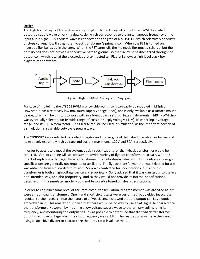
Design The high-level design of the system is very simple. The audio signal is input to a PWM chip, which outputs a square wave of varying duty cycle, which corresponds to the instantaneous frequency of the input audio signal. This square wave is connected to the gate of a MOSTFET, which selectively conducts or stops current flow through the flyback transformer's primary coil. When the FET is turned on, magnetic flux builds up in the core. When the FET turns off, the magnetic flux must discharge, but the primary coil does not provide a conductive path to ground, so the flux must be discharged through the output coil, which is what the electrodes are connected to. Figure 1 shows a high-level black box diagram of the system.
Figure 1: High-Level Black Box diagram of Singing Arc.
For ease of modeling, the LT6992 PWM was considered, since it can easily be modeled in LTSpice. However, it has a relatively low maximum supply voltage (5.5V), and is only available as a surface mount device, which will be difficult to work with in a breadboard setting. Texas Instruments' TL494 PWM chip was eventually selected, for its wide range of possible supply voltages (41V), its wider input voltage range, and its DIP16 form factor. The LT6992 can still be used in simulation, as the important portion of a simulation is a variable duty cycle square wave. The STP80NF12 was selected to control charging and discharging of the flyback transformer because of its relatively extremely high voltage and current maximums, 120V and 80A, respectively. In order to accurately model the system, design specifications for the flyback transformer would be required. Vendors online will sell consumers a wide variety of flyback transformers, usually with the intent of replacing a damaged flyback transformer in a cathode-ray television. In this situation, design specifications are generally not required or available. The flyback transformer that was selected for use was obtained from a discarded television. Sony was contacted for specifications, but since the transformer is both a high-voltage device and proprietary, Sony advised that it was dangerous to use in a non-intended way, and also proprietary, and so they would not provide its internal specifications. Because of this, a simulated model would not be possible based on ideal specifications. In order to construct some level of accurate computer simulation, the transformer was analyzed as if it were a traditional transformer. Open- and short-circuit tests were performed, but yielded inaccurate results. Further research into the nature of a flyback circuit showed that the output coil has a diode embedded in it. This realization showed that there would be no way to use an AC signal to characterize the transformer. However, by inputting a low-voltage square wave to the primary coil, varying its frequency, and monitoring the output coil, it was possible to determine that the flyback transformer output maximum voltage when the input frequency was 95kHz. This realization also made the idea of using a capacitive divider to characterize the turns-ratio invalid as well.
-12-
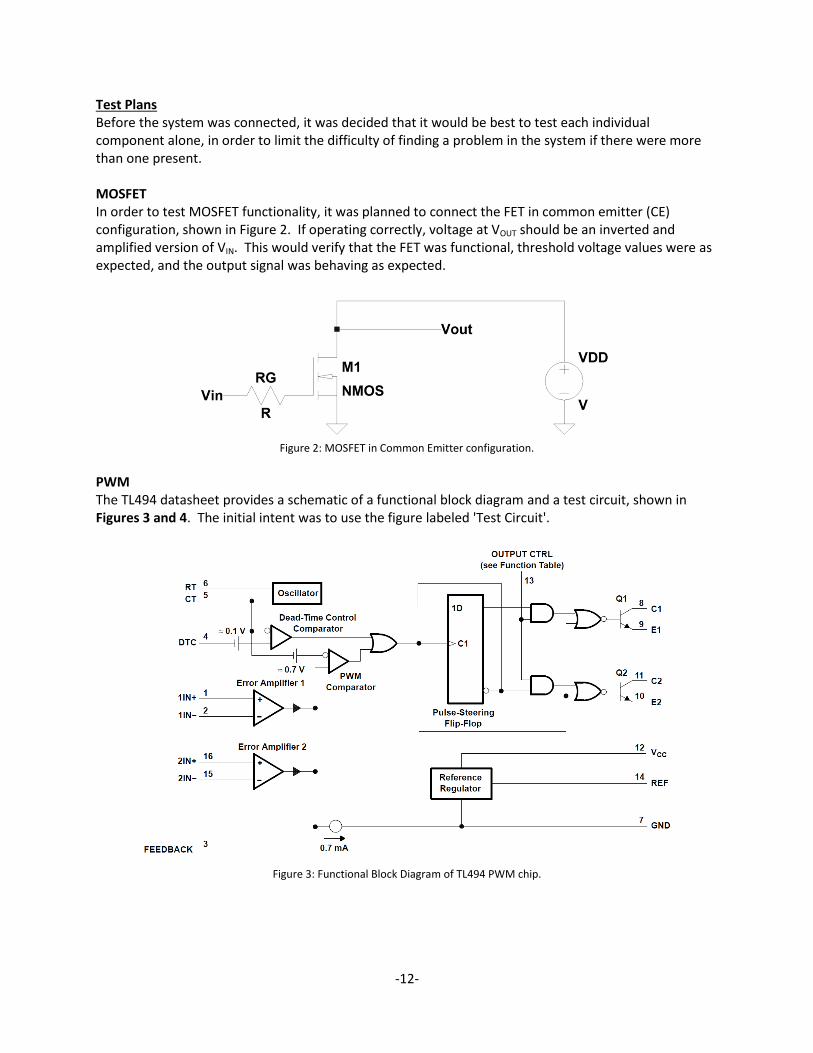
Test Plans Before the system was connected, it was decided that it would be best to test each individual component alone, in order to limit the difficulty of finding a problem in the system if there were more than one present. MOSFET In order to test MOSFET functionality, it was planned to connect the FET in common emitter (CE) configuration, shown in Figure 2. If operating correctly, voltage at VOUT should be an inverted and amplified version of VIN. This would verify that the FET was functional, threshold voltage values were as expected, and the output signal was behaving as expected.
Figure 2: MOSFET in Common Emitter configuration.
PWM The TL494 datasheet provides a schematic of a functional block diagram and a test circuit, shown in Figures 3 and 4. The initial intent was to use the figure labeled 'Test Circuit'.
Figure 3: Functional Block Diagram of TL494 PWM chip.

-13-
Figure 4: TL494 Test Circuit.
Input Protection Since the system will be conducting high voltages an currents, the possibility of a errant voltage or current spike propagating backwards through the system is a remote possibility. For this reason, a unity gain buffer is planned to be inserted between the input audio signal and the PWM, in the hopes that should such a spike occur, the buffer will protect the input device. Additionally, should the input audio signal be of low enough magnitude, the unity gain buffer can be replaced with an op-amp based amplifier to levels that the PWM can accurately utilize.
-14-
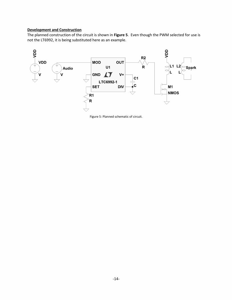
Development and Construction The planned construction of the circuit is shown in Figure 5. Even though the PWM selected for use is not the LT6992, it is being substituted here as an example.
Figure 5: Planned schematic of circuit.
-15-
Integration and Test Results MOSFET Testing of the FET did not go as expected. While the FET and resistor were connected and biased properly, the FET did not perform as expected. While the input signal was a square wave, the output signal showed significant oscillation, as well as the lack of a sufficiently fast turn-on and turn-off curve. It was at this time the capacitances were considered. The initial resistor, 5kΩ, was forming a low-pass filter with the gate-source capacitance, CGS (4300pF), with a cutoff frequency of 7.4kHz, far too low if the system was expected to pass up to a 20kHz signal (the assumed maximum frequency detectable by the human ear). Once this was realized, the gate-biasing resistor was changed to 100Ω, which resulted in a cutoff frequency of 370kHz, providing plenty of bandwidth, but allowing much more current to conduct through the FET. This additional current would cause more heat in the FET, so a heatsink would be applied to keep the FET from damaging itself. PWM Testing of the PWM did not go as expected. The Test Circuit given in the datasheet was the first configuration tested. Unfortunately, as shown in Figure 4, although pins 3 and 4 are clearly labeled as test inputs, the datasheet was vague on how to use these test inputs, especially given the fact that pins 1, 2, 15, and 16 are labeled as input pins. Several different variations of this test circuit was used, but a functional configuration could not be found. The next plan would simply be to use the pins labeled as 1in- and 1in+ as input pins, and tie unused pins either to ground or supply as seemed appropriate. Again, several configurations were tested, but none were found to be functional. The functional block diagram (Figure 3) was then studied to construct an appropriate configuration. Again, no functional configuration could be found. However, analysis of the functional block diagram did provide enough insight into the PWM's logical functionality, that it was possible to modify the test circuit shown in Figure 4 in such a way as to yield a functional configuration, namely, to ground pin 4, dead-time control, and pin 13, output control. A DC voltage was supplied to pin 3, feedback, and pin 8, output 1, produced the variable duty cycle square wave required. The minimum duty cycle was found to be 15%, and began to rise when the DC voltage applied reached approximately .7V. It reached 100% duty cycle at approximately 2.2V. FET Driving the Transformer The initial configuration to test the FET driving the transformer had the positive terminal of the transformer's primary coil connected to a power supply, the negative terminal of the primary coil connected to the drain of the FET, the source terminal of the FET connected to ground, and the gate of the FET connected to a function generator, which would output a square wave of 6VPP, with a 3V offset, and variable frequency. The positive and negative terminals of the output coil of the transformer were each connected to an electrode (gas welding rod). This configuration worked intermittently, successfully generating a spark approximately 1cm long. It was not clear what caused the intermittent nature of the successful spark. However, the power supply was switching back and forth between current-controlled and voltage-controlled modes rapidly and
-16-
violently, therefore, in order to avoid the possibility of damaging it, it was decided to power the circuit afterward with a car battery. Upon the successful, though intermittent, test, the PWM output was connected to gate of the FET, which continued to intermittently drive a spark across the electrodes. Power Supplies Further testing began to fail, and it was unclear why. Eventually, since the test configuration was not working, testing resumed using a standard power supply. Testing of individual components isolated from other components continued to fail. Varied testing across various labs and lab equipment eventually revealed that, out of several models, only a single model of power supply available was capable of outputting enough power to drive either the FET or the PWM, as they were both drawing approximately 1.5A and 12V (18W), and it appeared that most of the power supplies available were only capable of outputting up to 5W. Once this was discovered, it became apparent that the car battery must be used to supply power to any test configurations. FET Capacitances Further testing, using the car battery to power tests, continued to perform in an intermittent fashion, and then failed altogether. It was decided to drive the transformer directly from the PWM. While this approach did burn out two PWM chips, it did function in a reliable manner, which indicated that there was something wrong with the FET which caused the intermittent successful operation. Deeper analysis of the FET datasheet showed relatively very high capacitance ratings. To test if it indeed was the FET's capacitances that were preventing the transformer from discharging enough voltage to cause a spark, the PWM used to drive the transformer, which produced a spark, and then capacitors in the amount of the FET's capacitance were added in parallel with the PWM's output, and the transformer failed to produce a spark. The capacitance in the FET must have caused some sort of L-C resonance with the inductance of the transformer, and prevented successful discharge of the transformer. New FET Since the chosen FET possessed far too high capacitances to drive the transformer, and new FET had to be chosen. The STP22NF03L was chosen. It's maximum voltage and current ratings are 30V and 22A, not as high as the STP80NF12, but still higher than would likely be required. It also displays far lower capacitances, a CGS of 330pF, and CDS of 90pF. Additionally, a 3.5mF bypass capacitor was connected between the positive and negative terminals to eliminate any noise present in the supply voltage. Testing Resumed Testing the new FET in CS mode produced expected results. However, inserting it into the complete circuit did not yield a spark at the output. After much trial and error, the individual test leads were tested, and several were found to present unexpected resistance. Additionally, the test leads being used were very small gauge, and it was assumed that they were not capable of carrying enough current to sufficiently drive the transformer. Larger gauge test leads were acquired, and testing resumed. Since the new FET had such drastically lower CGS, it was decided to implement a larger gate resistor to reduce the amount of current being drawn by the FET. As a control experiment, the complete circuit was connected and powered on. Almost immediately, the FET exploded. Apparently, the test leads used earlier were not capable of conducting enough current, whereas the larger gauge leads could. The damaged FET was replaced, and the gate resistor was increased from 100Ω to 10kΩ. Coupled with the FET's CGS of 330pF, the pair would create a low-pass filter with a cutoff frequency of 48.2kHz, high
-17-
enough to provide no interference from an audio signal that will not pass 20kHz. Upon powering the system up again, the FET again almost immediately exploded. Since the car battery was only providing 12V, the system must have been drawing far too much current. Current Limiting FET Since the system was drawing damaging amounts of current, a way to limit that current needed to be implemented. It was decided to connect another FET in series with the current FET. This secondary FET would be driven with a 95kHz square wave, which would keep the transformer working at its optimal frequency, and prevent too much current from flowing when the duty cycle became too short during a low-frequency audio input. The new configuration had the positive terminal of the primary transformer coil connected to the positive terminal of the battery, the negative terminal of the primary transformer coil connected to the drain of the current-limiting FET, source of the current-limiting FET connected to the drain of the audio input FET, and the source of the audio input FET connected to ground. The 3.5mF bypass capacitor is connected between the battery terminals, the current-limiting FET is driven by a 95kHz square wave of sufficiently high voltage to overcome its threshold voltage, and the audio input FET is driven by the PWM output. For testing, the PWM input is supplied with a DC voltage such that it outputs a 50% duty cycle output. This configuration successfully produced a stable 1cm standing arc between the electrodes, with a minimum of heat evidenced in the FET heatsinks. Audio Input Since the audio output capability of the cell phone used to source an audio signal is only a maximum of 600mV, and the PWM operates with input voltages ranging from .5V to 2.2V, the signal would be passed through a voltage divider to offset it high enough to activate the PWM comparison. When the audio signal was applied, it provided enough voltage to activate the PWM and produce a stable spark, but did not produce audible results. Time Limit Reached A great deal of time was wasted before discovering that the original FET capacitances were to blame for the non-functionality of the system. After the discovery, significant strides in development were made at a consistent rate. Future Plan of Action The inclusion of the current-limiting FET solved the problem of drawing too much current. However, its inclusion requires the inclusion of an external input signal, the 95kHz square wave. This requirement can be resolved by including a crystal oscillator coupled with an appropriately configured voltage comparator and an op-amp based amplifier to provide the control signal. Since the audio signal by itself is not of high enough amplitude to activate the PWM's comparators, it will need to be conditioned. A simple op-amp based amplifier can increase the amplitude of the signal that it is high enough to swing between the PWM's minimum and maximum comparator values, as well as provide input protection for the audio signal source device. Since the audio signal is an AC value, the negative portions of the signal will not be considered by the PWM. For this reason, the audio signal should be passed through a full wave rectifier. If the gain in the amplifier is high enough, the signal will be still be of sufficient magnitude after the voltage drop incurred by the rectifier's diodes. Lastly, since the PWM's minimum compare value is not zero, the rectified audio signal must be offset. This can easily be accomplished by the use of a voltage divider.

-18-
Conclusion While the project was not able to be completed in the allotted time, it was still an excellent learning opportunity. Thus far in my coursework, many variables need not have been considered. FET capacitance ratings have been discussed in lecture, but the impact of those capacitances have never been evidenced. This experience will ensure I will never overlook formerly irrelevant details. It had also been assumed that test leads should provide adequate conductance for any range of voltage and current. Once again, a formerly irrelevant detail. Lastly, assuming that all power supplies are created equal wasted valuable time. Whenever possible, initial power dissipation calculations should be done and compared to the supply capabilities.

-19-
Bibliography [1] R. Ford and C. Coulston, Design for Electrical and Computer Engineers, McGraw-Hill, 2007. [2] IEEE Std 1233, 1998 Edition, p. 4 (10/36), DOI: 10.1109/IEEESTD.1998.88826 [3] E. Kuffel and W.S. Zaengl, High Voltage Engineering Fundamentals. Pergamon Press, 1984. [4] Mohammad Khalifa, High Voltage Engineering: Theory and Practice. Cairo University, Giza, Egypt, 1990. [5] T. J. Gallagher, Department of Electrical Engineering, University College, Dublin. A. J. Pearmain, Department of Electrical and Electronic Engineering, Queen Mary College, University of London. High Voltage: Measurement, Testing and Design. 1983, John Wiley and Sons, LTD. [6] Naito, Kenji and Takiguchi, Hisashi, of Murata Manufacturing Co., Flyback Transformer. US Patent # 6,850,143, February 1, 2005. [7] Bondar, Henri B., Process and device for converting a periodic LF electric voltage into sound waves. US Patent #4,460,809. July 17, 1984. [8] Siegfried, Klein, Electrical Transducer. US Patent #2,768,246. October 23, 1956. [9] Torn, William R. of Dukane Corporation, Inertialess Transducer. US Patent #3,105,124. September 24, 1963. [10] Daniel Schoo. (10.20.2013). DuKane Ionovac: The History of a Brilliant Failure. Available: http://www.ionovac.com/dshistory1.htm [11] Plasmana. (10.20.2013). The Plasma Speaker. Available: http://www.instructables.com/id/Build-A-Plasma-Speaker/ [12] Dr Scott M. Baker. (10.20.2013) Plasma Speaker. Available: http://www.smbaker.com/plasma-speaker [13] Author Unknown. (10.20.2013) LTC6992-1/LTC6992-2/LTC6992-3/LTC6992-4 Voltage-Controlled Pulse Width Modulator (PWM), Linear Technology. Available: http://www.linear.com/docs/29337 [14] Chung, S. K. Transient characteristics of high-voltage flyback transformer operating in discontinuous conduction mode. Electric Power Applications, IEE Proceedings - (Volume:151 , Issue: 5 ), September 9, 2004. [15] Author Unknown. (12.6.2013) Environmental Impact of Arc Suppression, Arc Suppression Technologies. Available: http://arcsuppressiontechnologies.com/images/4_LN106rvA.pdf [16] Author Unknown. (12.6.2013) Health Aspects of Air Pollution with Particulate Matter, Ozone and Nitrogen Dioxide, World Health Organization. Available: http://www.euro.who.int/__data/assets/pdf_file/0005/112199/E79097.pdf

-20-
[17] Szente, Munz, Drouet. Electrode erosion in plasma torches, Plasma Chemistry and Plasma Processing, Vol 12, No 3, 1992. Available: http://link.springer.com/article/10.1007%2FBF01447029 [18] Cushing, Tracy A. (12.6.2013) Electrical injuries in emergency medicine, Medspace.com. Available: http://emedicine.medscape.com/article/770179-overview#aw2aab6b2b2
-21-
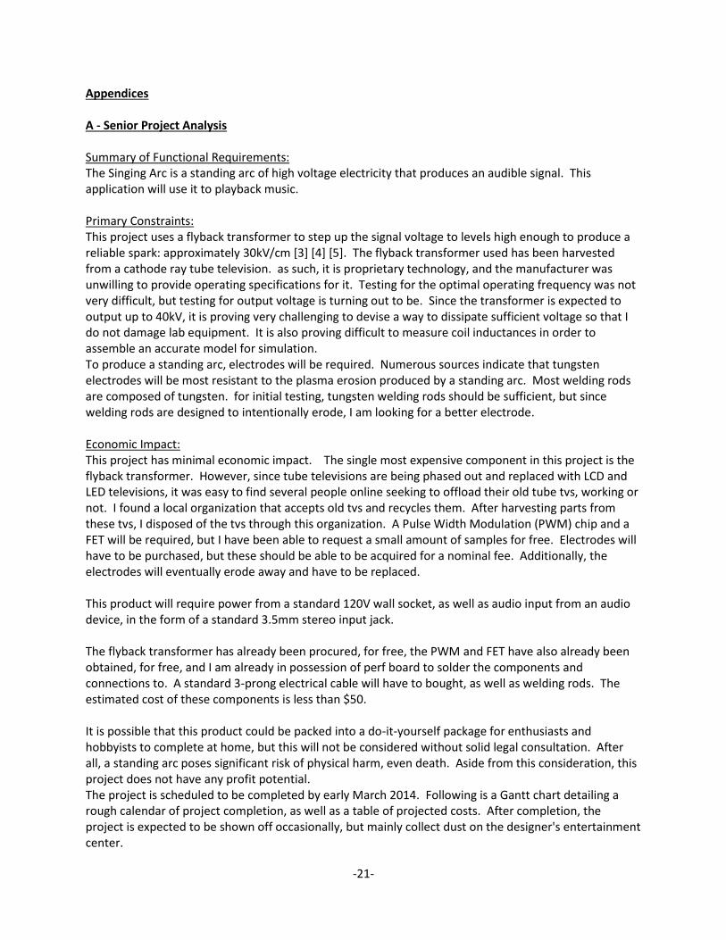
Appendices A - Senior Project Analysis Summary of Functional Requirements: The Singing Arc is a standing arc of high voltage electricity that produces an audible signal. This application will use it to playback music. Primary Constraints: This project uses a flyback transformer to step up the signal voltage to levels high enough to produce a reliable spark: approximately 30kV/cm [3] [4] [5]. The flyback transformer used has been harvested from a cathode ray tube television. as such, it is proprietary technology, and the manufacturer was unwilling to provide operating specifications for it. Testing for the optimal operating frequency was not very difficult, but testing for output voltage is turning out to be. Since the transformer is expected to output up to 40kV, it is proving very challenging to devise a way to dissipate sufficient voltage so that I do not damage lab equipment. It is also proving difficult to measure coil inductances in order to assemble an accurate model for simulation. To produce a standing arc, electrodes will be required. Numerous sources indicate that tungsten electrodes will be most resistant to the plasma erosion produced by a standing arc. Most welding rods are composed of tungsten. for initial testing, tungsten welding rods should be sufficient, but since welding rods are designed to intentionally erode, I am looking for a better electrode. Economic Impact: This project has minimal economic impact. The single most expensive component in this project is the flyback transformer. However, since tube televisions are being phased out and replaced with LCD and LED televisions, it was easy to find several people online seeking to offload their old tube tvs, working or not. I found a local organization that accepts old tvs and recycles them. After harvesting parts from these tvs, I disposed of the tvs through this organization. A Pulse Width Modulation (PWM) chip and a FET will be required, but I have been able to request a small amount of samples for free. Electrodes will have to be purchased, but these should be able to be acquired for a nominal fee. Additionally, the electrodes will eventually erode away and have to be replaced. This product will require power from a standard 120V wall socket, as well as audio input from an audio device, in the form of a standard 3.5mm stereo input jack. The flyback transformer has already been procured, for free, the PWM and FET have also already been obtained, for free, and I am already in possession of perf board to solder the components and connections to. A standard 3-prong electrical cable will have to bought, as well as welding rods. The estimated cost of these components is less than $50. It is possible that this product could be packed into a do-it-yourself package for enthusiasts and hobbyists to complete at home, but this will not be considered without solid legal consultation. After all, a standing arc poses significant risk of physical harm, even death. Aside from this consideration, this project does not have any profit potential. The project is scheduled to be completed by early March 2014. Following is a Gantt chart detailing a rough calendar of project completion, as well as a table of projected costs. After completion, the project is expected to be shown off occasionally, but mainly collect dust on the designer's entertainment center.
-22-
Figure 6: Project Gantt chart.
-23-
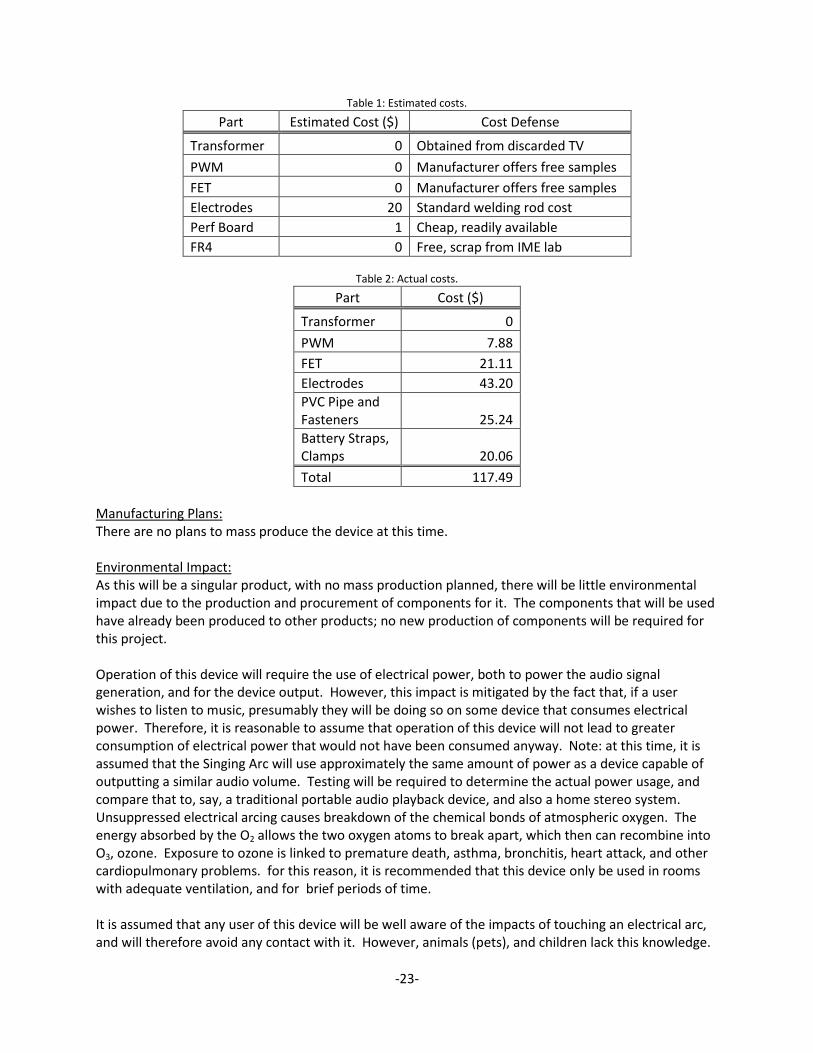
Table 1: Estimated costs.
Part Estimated Cost ($) Cost Defense
Transformer 0 Obtained from discarded TV
PWM 0 Manufacturer offers free samples
FET 0 Manufacturer offers free samples
Electrodes 20 Standard welding rod cost
Perf Board 1 Cheap, readily available
FR4 0 Free, scrap from IME lab
Table 2: Actual costs.
Part Cost ($)
Transformer 0
PWM 7.88
FET 21.11
Electrodes 43.20
PVC Pipe and Fasteners 25.24
Battery Straps, Clamps 20.06
Total 117.49
Manufacturing Plans: There are no plans to mass produce the device at this time. Environmental Impact: As this will be a singular product, with no mass production planned, there will be little environmental impact due to the production and procurement of components for it. The components that will be used have already been produced to other products; no new production of components will be required for this project. Operation of this device will require the use of electrical power, both to power the audio signal generation, and for the device output. However, this impact is mitigated by the fact that, if a user wishes to listen to music, presumably they will be doing so on some device that consumes electrical power. Therefore, it is reasonable to assume that operation of this device will not lead to greater consumption of electrical power that would not have been consumed anyway. Note: at this time, it is assumed that the Singing Arc will use approximately the same amount of power as a device capable of outputting a similar audio volume. Testing will be required to determine the actual power usage, and compare that to, say, a traditional portable audio playback device, and also a home stereo system. Unsuppressed electrical arcing causes breakdown of the chemical bonds of atmospheric oxygen. The energy absorbed by the O2 allows the two oxygen atoms to break apart, which then can recombine into O3, ozone. Exposure to ozone is linked to premature death, asthma, bronchitis, heart attack, and other cardiopulmonary problems. for this reason, it is recommended that this device only be used in rooms with adequate ventilation, and for brief periods of time. It is assumed that any user of this device will be well aware of the impacts of touching an electrical arc, and will therefore avoid any contact with it. However, animals (pets), and children lack this knowledge.
-24-
Therefore it is recommended that those with pets or children should not activate this device while those pets or children are present. Manufacturability: The Singing Arc does not contain many components, and none of the components are exotic or difficult to procure. Therefore, once a supplier of flyback transformers can be contracted with, manufacturability viable possibility. However, due to the risks of producing a standing arc, both physical and environmental, the legal issues surrounding the mass distribution and use make mass production of the Singing Arc not warranted. Sustainability: Exposure to plasma, and the high temperatures that come with it, cause the electrodes producing that plasma to melt away [17]. Lower power arcs will decrease that heat, but not to the point where the electrodes will not 'wear out.' It will be necessary to occasionally replace the electrodes. Fortunately, this should only be a matter of unscrewing the old one from its mount, and screwing in a new one. Use of any electronic device will consume electrical power. Since this desired output of this device, an audible signal, can already be obtained from numerous devices, the Singing Arc will not create a market for a new experience (listening to music), only deliver it in a unique manner. that is to say, if a person wishes to listen to music, they already can, and presumably would. Therefore, the aforementioned music lover would already be consuming electric power. To provide a higher audio volume required greater power transmitted through the arc. Transmitting greater power through the arc will cause increased degradation of the electrodes. Therefore, if an electrode capable of withstanding greater heat for longer periods of time can be found or designed, the Singing Arc would last longer, and produce a louder playback. Ethical Impact: From the first point in the IEEE's Code of Ethics [2]:
"to accept responsibility in making decisions consistent with the safety, health, and welfare of the public, and to disclose promptly factors that might endanger the public or the environment"
The introduction of a device into a household that has the very real possibility of harming or killing the user, the user's children, or the user's pets would be a very unethical thing to seriously consider. Furthermore, it certainly has serious potential legal ramifications. For these reasons, this project is largely a proof-of-concept project and will not be considered for mass production. As the designer, I am fully aware of the risks involved of using the device and do not hold any person or entity responsible for any injuries that may occur from its use. Health and Safety: At this time, it is unknown the precise amount of current that will be conducted through the arc. It is known that between 30kV and 40kV is expected. Neglecting the amount of current, coming into physical contact with that much voltage is sure to cause injury [18]. Even if the device is powered down, the electrodes will still be extremely hot, and able to cause burns.

-25-
Even if a cage of some sort where implemented around the arc, it would still produce ozone in some amount. Eventually, that ozone buildup will cause respiratory complications. in short, the operation of this device poses numerous risks to the health and safety of the user. Social and Political Impact: The Singing Arc has little, if any, negative social or political impact. being exposed to a miniature lightning bolt that plays music will most likely be described as a positive experience. Social and political responsibility are of greater importance. The knowledge of how to create a dangerous electrical arc should be restricted to individuals that can exercise good judgment in how to use it, and not abuse it. If the ethical and legal consequences of distributing the Singing Arc were to be resolved, I believe there would be two specific groups that it may be marketed to: hobbyist do-it-yourselfers, and high end clients with a taste for exotic or eccentric products. on a manual-scale production level, a device can reasonably be expected to produced for between $50 and $100. The scarcity of competitive products can justify a sale price of up to $300. If adequate cooling systems can be integrated into the system, and more durable electrodes can be implemented, a significantly larger spark can be produced, and provide a higher audio volume. The high-end client, presumably having higher discretionary capital, might not flinch at a price approaching $1,000. on such a small scale production run, the designer might net a few thousand dollars a year, but likely not earn enough to turn production into a full-time job. Development: Testing the flyback transformer to determine its turn ratio, primary, secondary, and mutual inductances is proving to be much more difficult than had been expected. Given that the producer of the transformer is unwilling to provide technical details, the testing is important, so that an accurate simulation model is possible. Determining the turn ratio is a relatively simple process: put an ac voltage on the primary side, observe the secondary side. The trouble here is that the multimeters I have access to can only measure up to 1kVAVERAGE. Inputting 10VPP to the primary side produces more than 700VPP on the secondary side. upon completion, I will be applying 120VRMS to the input. Using this method will be impossible without introducing some new variable. First, a high voltage resistive divider appeared to be a viable possibility. However, it was decided that the price for a pair of resistors was too high (up to $100). Currently, I am investigating the possibility of using a capacitive divider. Since the 10V input trial identified that maximum output at a relatively high frequency, 95kHz, only small capacitor values will be required. More information regarding this method will be available at a later date. Measuring the transformer's inductances is also proving to be more difficult than was first expected. Due either to high use and/or abuse, or some unknown property of the transformer, I have been unable to get accurate, repeatable readings of inductances from the impedance bridges available to me. I have
been pursuing a procedure based on the voltage drop across an inductor,
, which uses a
function generator and an oscilloscope to measure voltage levels and phase variances to determine the inductance. at this time, a few messy procedures have been identified, and I am attempting to develop a more formalized, easy to follow procedure. More information will be available at a later date.
-26-
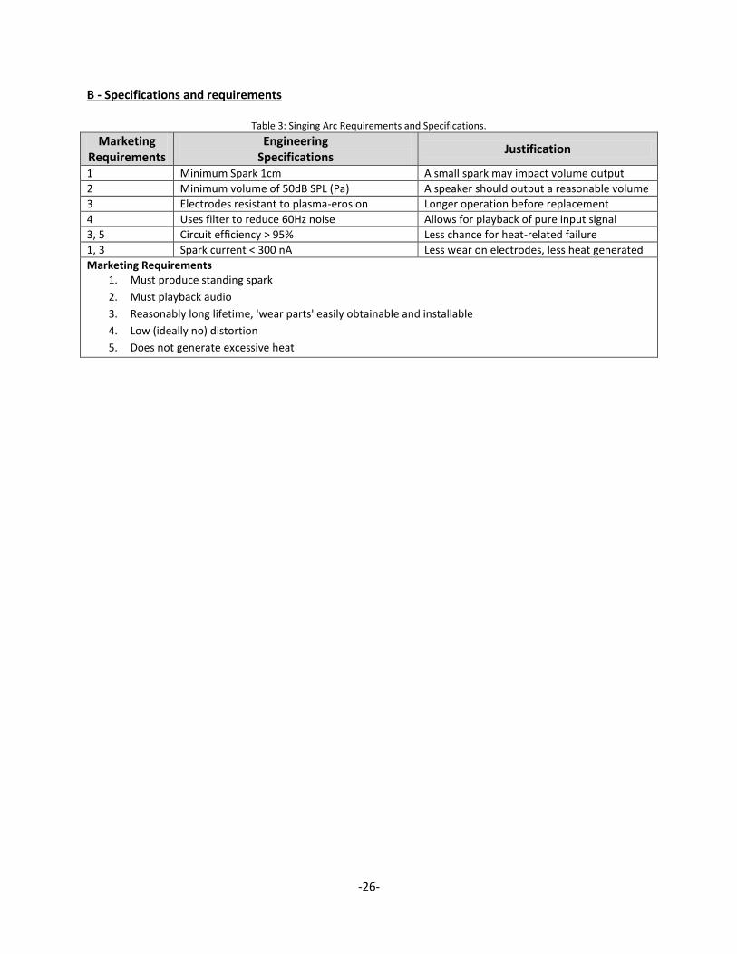
B - Specifications and requirements
Table 3: Singing Arc Requirements and Specifications.
Marketing Requirements
Engineering Specifications
Justification
1 Minimum Spark 1cm A small spark may impact volume output
2 Minimum volume of 50dB SPL (Pa) A speaker should output a reasonable volume
3 Electrodes resistant to plasma-erosion Longer operation before replacement
4 Uses filter to reduce 60Hz noise Allows for playback of pure input signal
3, 5 Circuit efficiency > 95% Less chance for heat-related failure
1, 3 Spark current < 300 nA Less wear on electrodes, less heat generated
Marketing Requirements 1. Must produce standing spark
2. Must playback audio
3. Reasonably long lifetime, 'wear parts' easily obtainable and installable
4. Low (ideally no) distortion
5. Does not generate excessive heat

-27-
C - Parts List and Costs
Table 3: Estimated costs.
Part Estimated Cost ($) Cost Defense
Transformer 0 Obtained from discarded TV
PWM 0 Manufacturer offers free samples
FET 0 Manufacturer offers free samples
Electrodes 20 Standard welding rod cost
Perf Board 1 Cheap, readily available
FR4 0 Free, scrap from IME lab
Table 4: Actual costs.
Part Cost ($)
Transformer 0
PWM 7.88
FET 21.11
Electrodes 43.20
PVC Pipe and Fasteners 25.24
Battery Straps, Clamps 20.06
Total 117.49

-28-
D - Schedule - Time Estimates
Figure 7: Project Gantt Chart.
-29-
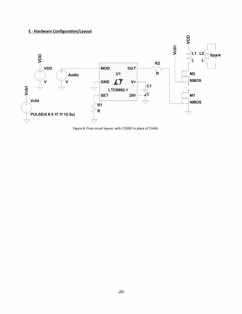
E - Hardware Configuration/Layout
Figure 8: Final circuit layout, with LT6992 in place of TL494.