simulation of geometry and shadow effects...
TRANSCRIPT

SIMULATION OF GEOMETRY AND SHADOW EFFECTS IN 3D
ORGANIC POLYMER SOLAR CELLS
_______________
A Thesis
Presented to the
Faculty of
San Diego State University
_______________
In Partial Fulfillment
of the Requirements for the Degree
Master of Science
in
Mechanical Engineering
_______________
by
Mihir Prakashbhai Parikh
Spring 2013


iii
Copyright © 2013
by
Mihir Prakashbhai Parikh
All Rights Reserved

iv
DEDICATION
I would like to dedicate this thesis to my biggest support my family in India.

v
Whatever you do will be insignificant, but it is very important that you do it.
-Mahatma Gandhi

vi
ABSTRACT OF THE THESIS
Simulation of Geometry and Shadow Effects in 3D Organic Polymer Solar Cells
by Mihir Prakashbhai Parikh
Master of Science in Mechanical Engineering San Diego State University, 2013
Rising inventory levels of Solar panels and new production capacity is driving solar PV prices lower and thereby, bringing solar energy closer to grid price parity. Major studies have been made in improving solar cell efficiency. A novel approach based on three-dimensional (3D) architecture for polymeric photovoltaic cells made up of an array of sub-micron and nano-pillars which not only increase the area of the light absorbing surface, but also improve the carrier collection efficiency of bulk-heterojunction organic solar cells. This study concentrates on modeling the effect of shading on 3D solar cell by varying arrangements of pillars/electrodes on a 3D organic photovoltaic cell surface. We have developed mathematical model in MATLAB which simulate the shadow effect and characterize the cell geometrically by varying aspect ratio, spacing, size, shape. A Model has been built for several shading profiles to optimize the exposed area on solar cell for different position of sun.

vii
TABLE OF CONTENTS
PAGE
ABSTRACT ............................................................................................................................. vi
LIST OF TABLES ................................................................................................................... ix
LIST OF FIGURES ...................................................................................................................x
ACKNOWLEDGEMENTS .................................................................................................... xii
CHAPTER
1 INTRODUCTION .........................................................................................................1
1.1 Solar Cell ...........................................................................................................2
1.2 Novel Approach For Improve Photovoltaic Efficiency of Solar Cell ................3
1.3 Motivation for Research ....................................................................................3
1.4 Focus of Current Research .................................................................................5
2 LITERATURE SURVEY ..............................................................................................7
2.1 Organic Solar Cell ..............................................................................................7
2.2 Organic Solar cell Device Architecture .............................................................8
2.2.1 Single Layer Organic Solar Device ..........................................................8
2.2.2 Bilayer Device(Heterojunction) Solar Device ..........................................9
2.2.3 Bulk Heterojunction Organic Solar Device ............................................10
2.3 Steps Involved in Generaing Electricity from Organic Solar Cell ..................11
2.4 Work Function of Polymer Material ................................................................12
2.5 Geometric Characterization of 3D Solar cell ...................................................13
2.6 Benefits of Geometrical Characterization of 3D Solar Cell ............................13
3 THEORY OF 3D ORGANIC PHOTOVOLTAIC CELL ...........................................15
3.1 3D Organic Solar Device .................................................................................17
3.2 Organic Materials Used in 3D Organic Solar Cell ..........................................19
3.2.1 SU-8 (Negative Photoresist) ...................................................................19
3.2.2 PEDOT:PSS [Poly(3,4-ethylenedioxythiophene) poly(styrenesulfonate)] ....................................................................................20
3.2.3 P3HT:PCBM ...........................................................................................20

viii
4 MICROFABRICATION PROCESS ...........................................................................22
4.1 3D Solar Cell Fabrication ................................................................................22
4.2 Lithography Process.........................................................................................23
4.2.1 Step-1 Substrate Pretreatment .................................................................24
4.2.2 Step-2 Spin Coating ................................................................................24
4.2.3 Step-3 Softbake .......................................................................................24
4.2.4 Step-4 Exposure ......................................................................................25
4.2.5 Step-5 Post Exposure Bake (PEB): .........................................................26
4.2.6 Step-6 Development................................................................................27
4.2.7 Step-7 Hard Baking.................................................................................28
4.3 Spin Coating of PEDOT: PSS & Heat Treatment ...........................................29
4.4 Spin Coating of P3HT:PCBM & Heat Treatment ...........................................30
4.5 Aluminum Deposition ......................................................................................30
5 GEOMETRICAL CHARACTERIZATION OF 3D ARCHITECTURE ....................31
5.1 Terminologies for Characterization .................................................................32
5.2 Description of 3D Solar Cell Geometry ...........................................................33
5.3 Generation-I Solar Cell ....................................................................................34
5.3.1 Experimental Setup .................................................................................34
5.3.2 Control Parameters and Results ..............................................................34
5.3.3 Results & Discussion ..............................................................................34
5.4 Generation II Solar Cell ...................................................................................36
5.4.1 Model for Simulation of Generation-II Solar Cell ..................................36
5.4.2 Mathematical Model for Generation II ...................................................37
5.4.3 Calculate the Shadow for Horizontal Surface .........................................37
5.5.4 Calculate the Shadowed Vertical Surface ...............................................39
5.4.5 Simulation Results and Discussion of 3D Solar Cell..............................40
6 CONCLUSION ............................................................................................................45
REFERENCES ........................................................................................................................48
APPENDIX
PROGRAM CHHAYA ......................................................................................................52

ix
LIST OF TABLES
PAGE
Table 1.1. Characteristics Comparison of 2-D OPV with 3D OPV ...........................................5
Table 2.1. Organic Solar Cell Material ......................................................................................8
Table 4.1. Soft Baking Parameters of SU-8 .............................................................................24
Table 5.1. Results from Quasi-Regular Design .......................................................................41
Table 5.2. Result from Staggered Design ................................................................................43
x
LIST OF FIGURES
PAGE
Figure 1.1. Renewable energy outlooks. ....................................................................................1
Figure 1.2. Solar installed capacity. ...........................................................................................2
Figure 1.3. Architecture of 3D OPV (Organic Photovoltaic’s). ................................................3
Figure 1.4. Concept of reflection on 3D solar cells. ..................................................................4
Figure 1.5. Research roadmap, MEMS research group, SDSU. ................................................6
Figure 2.1. Structure of 2D organic solar cell. ...........................................................................7
Figure 2.2. Charge generation process in a single layered OPV device. ...................................9
Figure 2.3. Charge generation process in a bulk heterojuntion device. ...................................10
Figure 2.4. Organic solar cell architecture. ..............................................................................11
Figure 2.5. Work function of polymer material. ......................................................................12
Figure 3.1. 3D representations of ‘AllPolyPV” solar cell architecture with 3D pyrolysed carbon electrodes and a photoactive matrix. ...............................................15
Figure 3.2. Fermi energy level diagrams and light harvesting relative to vacuum level for the AllPoly3DPV system in flat band conditions. ..................................................17
Figure 3.3. Device structure of 3D organic polymer solar cell. ...............................................18
Figure 3.4. Chemical structure SU-8 (negative photoresist). ...................................................19
Figure 3.5. Chemical structure of (1) PEDOT & (2) PSS, Hiroshima University, Applied Chemistry Department. ..................................................................................20
Figure 3.6. Chemical Structure of P3HT: PCBM. ...................................................................21
Figure 4.1. Layers of 3D phtovoltaic cell. ...............................................................................22
Figure 4.2. Lithography process. .............................................................................................23
Figure 4.3. Steps for photolithography. ...................................................................................23
Figure 4.4. Soft baking of SU-8 on a hot-plate. .......................................................................25
Figure 4.5. UV light. ................................................................................................................26
Figure 4.6. SEM image of high aspect ratio SU-8. ..................................................................27
Figure 4.7. Post exposure bake effect with proper bake condition (a) and (b) aggressive bake condition. ...........................................................................................27
Figure 4.8. SEM image of SU-8 pillar after development. ......................................................28

xi
Figure 4.9. SEM image of pillar after hard baking. .................................................................29
Figure 4.10. Spin coating of PEDOT:PSS & Heat treatment. .................................................29
Figure 4.11. Spin coating of P3HT: PCBM & heat treatment. ................................................30
Figure 4.12. Solar cell after aluminum deposition. ..................................................................30
Figure 5.1. Various SUN angle. ...............................................................................................33
Figure 5.2. (A) Schematic diagram of generation-I (1cm*1cm). ............................................33
Figure 5.3. (A) Signatone probe station & light source. ..........................................................35
Figure 5.4. Microscopic image of solar cell at different horizontal angles. ............................35
Figure 5.5. Results of optical imaging generation- I. ..............................................................36
Figure 5.6. (1) Quasi- regular array design. (2) Staggered array design. ................................37
Figure 5.7. Trigonometric formulas for horizontal surfaces on 3D solar chip. .......................38
Figure 5.8. Calculate side PC & PB of triangle OPC. .............................................................38
Figure 5.9. Trigonometric formula for vertical surfaces on 3D solar chip. .............................40
Figure 6.1. (1) Experimental result (image analysis). (2) PRO-E model. ...............................45
Figure 6.2. (A) PRO-E Model. (B) Mathematical model quasi-regular design. (C) Staggered design. .........................................................................................................47

xii
ACKNOWLEDGEMENTS
I would like to thank my thesis advisor, Dr. Samuel Kassegne, for providing me the
insight for this technology, guiding me through the steps to reach a goal, and assisting me
personally and professionally during this journey.
I would like to thank Mr. Nikit Shah, who taught me C Programming Language. I
also would like to thank my committee members, Professor Meharabadi and Professor Engin
for their valuable time and serving in my thesis committee.
I also would like to thank Dr. Steve Barlow for providing invaluable full access to the
Electron Microscope Facility, for always providing comprehensive assistance, and sharing
his enthusiasm for the research.
In addition, I would like to thank to my lab members at the MEMS Research Lab, for
their shared interest in the research and continual support. I also want to thank my
roommates.

1
CHAPTER 1
INTRODUCTION
In recent years, there has been a significant increase in interest in various forms of
renewable energy sources, which are seen as the key to long-term weaning from strict
reliance on fossil fuels such as oil, coal and natural gas [1].
Solar Photovoltaic [PV] energy is the most popular among the DER (Distributed
Energy resources) as you can (see Figure 1.1 [1]). This is mainly because solar energy is
sustainable and widely available everywhere. Solar energy uses a resource that is far larger
than required to provide all of the world’s energy. A simple calculation shows that the
amount of energy received in one hour by the earth from the sun is equivalent to world
energy consumption in one year. Unlike oil and gas, solar energy is available almost
everywhere. Unlike fossil fuels, solar energy has minimal environmental impacts. Solar is the
most democratic energy technology. No Increases in the cost of fuel, routine maintenance is
far less than conventional plants, and the fuel (sun energy) does not have to be transported [1,
2]. It produces no carbon footprint at all and requires very little energy to produce. There are
even government subsidiaries making solar panels commercially available.
Figure 1.1. Renewable energy outlooks. Source: U. S. Energy Information Administration. “International Energy Outlook 2011.” Last modified September 19, 2011. http://www.eia.gov/forecasts/ieo/pdf/0484(2011).pdf.

2
Solar electric energy demand has grown by an average 30% per annum over the past
20 years against a backdrop of rapidly declining costs and prices. This decline in cost has
been driven by economies of manufacturing scale, manufacturing technology improvements,
and the increasing efficiency of solar cells. Annual growth slowed down during the period
from 2007-2012, to 18.7%—down from 37.9% for the period from 2000-2007 (see Figure
1.2 [2]). This indicates that the industry is maturing and also indication of slower growth.
This is due to the volume of solar module being installed [2].
Figure 1.2. Solar installed capacity. Source: Hodge, Nick. “The Potential in Solar Stocks: Tends & Market Outlook.” Last modified August 29, 2008. http://www.energyandcapital.com/articles/the-potential-in-solar-stocks-trends-market-outlook/750.
1.1 SOLAR CELL
The search for low value cost photovoltaics has led investigator to organic materials
as possible candidates. The discovery of organic materials which have both conducting and
semiconductor properties has led to new and exciting possibilities. The main advantage of
organic materials is the ability to produce photovoltaic devices with different techniques,
such as ink jet printing or various roll to roll techniques, which could lead to very cheap, high
throughput manufacturing.

3
1.2 NOVEL APPROACH FOR IMPROVE PHOTOVOLTAIC
EFFICIENCY OF SOLAR CELL
The reduction of output power in solar cell can be attributed different factors but the
most important factor maximum power point (MPP) mismatch and shadows. If a solar cell is
partially shaded, some area will work as reverse bias working as resistance rather than power
generator. When reverse bias (or shaded area) exceeds the breakdown voltage of the solar
cell, the cell is damaged.
Unique approach 3D solar cells that capture nearly all the lights strike them to boost
the efficiency of photovoltaic cell. The new 3D solar cell capture photons from sunlight
using the pillar structure that resembles high rise building in a city efficiency improvements
by coating those materials with different photovoltaic materials. 3-D Organic Solar Cell is a
construction formed by a large array of high-aspect ratio SU-8 electrodes of 50-65 microns
diameter surrounded by a matrix of hetero-junction photoactive material. The depth of the
photo-active cell is around 110-130 microns. These 3-D electrodes are patterned with the
help of lithography process of SU-8 negative photo-resist [3-6] . The material on SU-8
pattern is deposited in three layers (see Figure 1.3). The new PV Cell consists of a polymer
precursor (SU-8) for the 3-D electrodes which are coated with layers of OrgaconTM as
anode, a photoactive polymer which is a blend of P3HT (poly (3-hexylthiophene) and PCBM
(phenyl-C61-butyric acid methyl ester) and aluminum as cathode [7].
Figure 1.3. Architecture of 3D OPV (Organic Photovoltaic’s).
1.3 MOTIVATION FOR RESEARCH
Major breakthrough made in solar cell efficiency, including increasing absorbance
efficiency of a cell by etching or texturing. In order to increase the absorbance efficiency of
solar cells, we have developed a three-dimensional solar cell structure by growing SU-8
4
pillar and depositing thin film overtop of SU-8 towers. These towers act as both scaffolding
and an electrical Interconnect. Multiple photon interactions as they reflect between these
towers increase absorption efficiency.
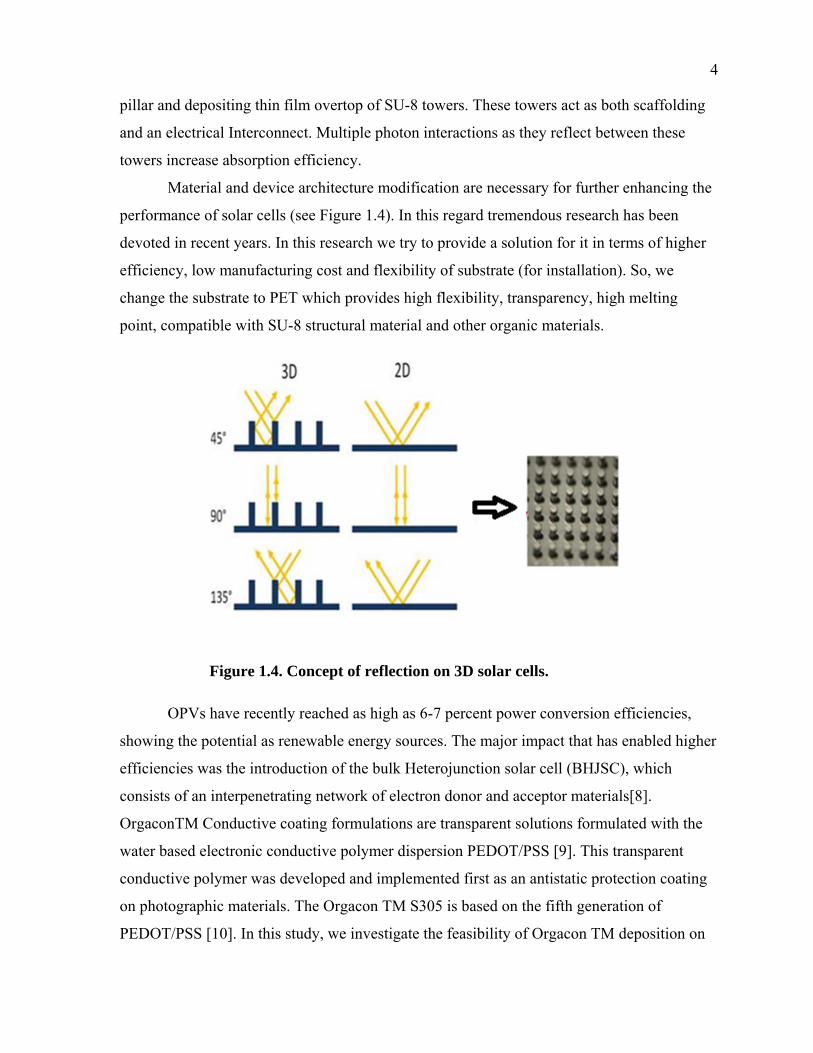
Material and device architecture modification are necessary for further enhancing the
performance of solar cells (see Figure 1.4). In this regard tremendous research has been
devoted in recent years. In this research we try to provide a solution for it in terms of higher
efficiency, low manufacturing cost and flexibility of substrate (for installation). So, we
change the substrate to PET which provides high flexibility, transparency, high melting
point, compatible with SU-8 structural material and other organic materials.
Figure 1.4. Concept of reflection on 3D solar cells.
OPVs have recently reached as high as 6-7 percent power conversion efficiencies,
showing the potential as renewable energy sources. The major impact that has enabled higher
efficiencies was the introduction of the bulk Heterojunction solar cell (BHJSC), which
consists of an interpenetrating network of electron donor and acceptor materials[8].
OrgaconTM Conductive coating formulations are transparent solutions formulated with the
water based electronic conductive polymer dispersion PEDOT/PSS [9]. This transparent
conductive polymer was developed and implemented first as an antistatic protection coating
on photographic materials. The Orgacon TM S305 is based on the fifth generation of
PEDOT/PSS [10]. In this study, we investigate the feasibility of Orgacon TM deposition on

5
negative photo resist SU-8 as a conductive polymer for 3-D OPV architecture. So here, the
research supports the use of 3-D material in comparison with 2-D with the help of a
comparison table (see Table 1.1). The primary purpose of the research is maintaining
flexibility and keeping the product ITO-free. So here we have used OrgaconTM as a
substitute of PEDOT: PSS and ITO. OrgaconTM tries to maintain the efficiency of solar cells
equivalent to that of the cells with ITO and PEDOT: PSS. The 3-D geometry of the
electrodes facilitates more absorption of light energy and increased charge collecting
efficiency [11].
Table 1.1. Characteristics Comparison of 2-D OPV with 3D OPV
Characteristics 2-D 3-D
Surface Area* 1 2.5 or more
No. of Reflections 0°<θ<45°→ 3 or more
0°<θ<90° → 1 45°<θ<90°→ 1 or 2
θ=90°→ 1
Angle Efficiency θ ≈ 90° 0°<θ<45° and 135°<θ<180°
Transparency Required Not Required
Electron Flow Vertical Horizontal
*Surface area calculated as real surface area of the photoactive film divided by projected surface area.
Organic Solar Cell project forms a significant component of the research done at Dr.
Samuel Kassegne’s MEMS Research Lab at SDSU. Figure 1.5 summarizes the roadmap for
the complete research going on in the MEMS Research Lab, SDSU for the all polymer PV
cells. The focus of this study is in the characterization and testing of the 3-D Organic
Photovoltaic Solar Cell.
The focus of the study is in geometrical modeling of shadow effects and it falls under
the modeling/simulation component (see Figure 1.5).
1.4 FOCUS OF CURRENT RESEARCH
The Thesis is arranged in the following sequence: Chapter 1 Presents introduction;
Chapter 2 Presents literature survey; Chapter 3 Covers Theory of 3D OPV, Chapter 4 Covers

6
Figure 1.5. Research roadmap, MEMS research group, SDSU.
the Micro fabrication; Chapter 5 Covers Geometrical characterization of 3D solar cell and
Conclusion.

7
CHAPTER 2
LITERATURE SURVEY
2.1 ORGANIC SOLAR CELL
Commonly materials used for solar cells are inorganic materials but the potential of
offering cheap and ease in processing turns industries interest in organic solar materials. The
basic phenomenon of the organic solar cell is to absorb the photons , knock out electrons,
drive the electrons between the polymer material of different work function; layers of
polymer material helps to improve the conductivity of the charge carriers, generate electricity
(see Figure 2.1).
Figure 2.1. Structure of 2D organic solar cell.
Organic based photovoltaic devices have several benefits like Ease in Manufacturing
and Low cost synthesis, as we can print the ink of organic photovoltaic material evaporate
without having a facility of high vacuum and temperature. Organic material has high
absorption coefficient, exceeding 10 5 cm-1Another major difference in crystalline inorganic
material and organic solar cell has small diffusion length of primary photo-excitation in this
material which is important for solar energy conversion process and usually high electric
field require to dissociate them into free charge carriers, due to this exciton binding energies
usually exceeding (see Table 2.1) [12].

8
Table 2.1. Organic Solar Cell Material
Layers Materials Characteristics
Bottom Layer Glass Transparent Base
1st Layer ITO Anode
2nd Layer PEDOT:PSS Conjugated Polymer
3rd Layer Active Layer Bulk Heterojunction Polymer
Top Layer Aluminum Cathode (Metal)
2.2 ORGANIC SOLAR CELL DEVICE ARCHITECTURE
Organic solar cell device architecture changed throughout the years from single layer
organic device and currently bulk heterojunction(BHJ) solar devices, which has more
fficiency compare to other organic device architecture.
2.2.1 Single Layer Organic Solar Device
In the first generation of conjugated polymer PV cells, a single layer of pure
conjugated polymer, e.g., poly(p-phenylene vinylene) (PPV), was sandwiched between
electrodes with different work functions, such as ITO and Al. Single layer is the simplest
Oragnic Photovoltaic device. The structures consist of only one semiconductor material and
are often referred as Schottky diodes [13]. The device consists of metal-insulator-metal
tunneling diode with asymmetrical work functions of metal electrodes. Due to forward bias,
holes from the high work function metal and electrons from the low work function metal are
directed into the thin film of a single layer component polymer semiconductor. Due to the
work function asymmetry of the cathode and anode, forward bias currents for a single carrier
type material are orders of magnitude larger than reverse bias currents at low voltages [14].
Under OPV short circuit conditions, the potential difference available in the single layered
device is generated by the difference between the work functions of the polymer electrodes,
in our case, PEDOT:PSS (Conjugated polymer) and Al [15, 16] (see Figure 2.2 [16]).
ɸ: Work Function - the energy needed to move an electron from the Fermi energy level into vacuum.
Eg: Bandgap - the amount of energy required to free an outer shell electron from its orbit around the nucleus to become a mobile charge carrier, able to move freely within the solid material.

9
Figure 2.2. Charge generation process in a single layered OPV device. Source: Brabec, C. J., N. Serdar Sariciftci, and Jan C. Hummelen. “Plastic Solar Cells.” Advanced Functional Materials 11, no.1 (2001): 15-26.
P+, P- : Positive and Negative Polarons - a slow moving electron.
CB: Conduction Band - the energy range that is higher than that of the valence band, sufficient to free an electron from binding with its atom.
VB: Valance Band - the energy range within which an electron is bonded to its atom.
2.2.2 Bilayer Device(Heterojunction) Solar Device
In a bilayer device, a donor and an acceptor material are stacked together with a
common interface. The charge separation occurs which is mediated by a large potential drop
between donor and acceptor. The bilayer is sandwiched between two electrodes matching the
donor HOMO and the acceptor LUMO, for efficient extraction of the corresponding charge
carriers. Neglecting all kinds of possible band bending due to energy level alignments [16,
17, 18]. Though the formation of a classical p/n-junction requires doped semiconductors with
free charge carriers to form the electric field in the depleted region, the charge transfer in
bilayer Heterojunction between undoped donor and acceptor materials is due to the
differences in the ionization potential and electron affinity of the adjacent materials. Upon
photon absorption in the donor D, the electron is excited from the HOMO to the LUMO [19].
If now an acceptor molecule A is in close proximity, the electron may be transferred to the
LUMO of A. A huge advantage over the single layer device is the monomolecular charge

10
transport, excitons dissociated at the material interface, the electrons travel within n-type
acceptor, and the holes travel within the p-type donor material. Hence holes and electrons are
transporting phases to contacts, mean donor and acceptor has to form continuous and
interpenetrating network [19, 20].
2.2.3 Bulk Heterojunction Organic Solar Device
Bulk Heterojunction is interpenetrating network of donor and acceptor junctions in a
bulk volume so that each donor-acceptor interface is within a distance less than the exciton
diffusion length and absorbing (Figure 2.3 [16]).
Figure 2.3. Charge generation process in a bulk heterojuntion device. Source: Brabec, C. J., N. Serdar Sariciftci, and Jan C. Hummelen. “Plastic Solar Cells.” Advanced Functional Materials 11, no.1 (2001): 15-26.
Bulk Heterojunction device is similar to the bilayer device, but it exhibits mainly
increased interfacial area where charge separation occurs. Due to interface being separated
through the volume no loss due to small Exciton diffusion length is expected, because all the
Excitons will be dissociated within their time period. In generating electricity from solar cell
concept (see Figure 2.4), the charges are also separated within the different phases: hence
recombination is reduced to a large extent often the photo-current follows the light intensity
linearly [17].

11
Figure 2.4. Organic solar cell architecture.
2.3 STEPS INVOLVED IN GENERAING ELECTRICITY FROM
ORGANIC SOLAR CELL
Absorption of Photons: Organic devices a small portion of the incident light is 1.absorbed. For example, a band gap of 1.1 eV is required to cover 75% of the AM1.5 solar photon flux; whereas most solution is processable semiconducting polymers (PPVs, poly (3-hexylthiophene) (P3HT)) have band gaps larger than 1.9 eV, which covers only 30% of the AM1.5 solar. Typically low charge carrier and Exciton mobility require layer thickness in the order of 100nm. Fortunately the absorption efficiency of organic materials is generally much higher so that only about 100nm are necessary to absorb between 60 and 90% if a reflective back contact is used [21].
Exciton Diffusion: Ideally, all photoexcited Excitons should reach a dissociation site. 2.Since such a site may be at the other end of the semiconductor. Their diffusion length should be at least equal the required layer thickness (for sufficient absorption) - otherwise they recombine and photons were wasted. Exciton diffusion ranges in polymers and pigments are typically around 10nm [17, 22]. However, some pigments like perylenes are believed to have Exciton diffusion lengths of several 100nm [21].
Charge separation: It is known to occur at organic semiconductor/metal interfaces, 3.impurities (e.g. oxygen) or between materials with sufficiently different electron affinities (EA) and ionization potentials (IA). In the latter one material can than act as electron acceptor (A) while the other keeps the positive charge and is referred to as electron donor (D) - since it did actually donate the electron to A. If the difference in IA and EA is not sufficient, the Exciton may just hop onto the material with the lower bandgap without splitting up its charges. Eventually it will recombine without contributing charges to the photocurrent [17, 21, 23].
Charge Transport: The transport of charges is affected by recombination during the 4.journey to the electrodes - particularly if the same material serves as a transport medium for both electrons and holes. Also, interaction with atoms or other charges

12
may slow down the travel speed and thereby limit the current - see also space charge limited current.
Charge Collection: In order to enter an electrode material with a relatively low work 5.function the charges often have to overcome the potential barrier of a thin oxide layer. In addition, the metal may have formed a blocking contact with the semiconductor so that they cannot immediately reach the metal.
2.4 WORK FUNCTION OF POLYMER MATERIAL
In Figure 2.5 the Fermi level energy diagram for polymer organic tandem structure is
been shown.
Figure 2.5. Work function of polymer material.
In an organic solar cell, only a small region of the solar spectrum is covered. For 1.example, a bandgap of 1.1 required to cover 77% of the AM1.5 (air mass) solar photon flux, whereas most solution processable semiconducting polymers (PPVs, poly(3-hexylthiophene) (P3HT)) have bandgap larger than 1.9 eV, which covers only 30% of the AM1.5. In addition, because of the low charge-carrier mobilities of most polymers, the thickness of the active layer is limited to 100 nm, which, in turn, results in absorption of only 60% of the incident light at the absorption maximum [24].
A Monte Carlo simulation study has been conducted to model bimolecular charge 2.recombination, treated as a random walk of a pair of charges in an energetically roughened landscape, with superimposed long-range coulomb interactions . This analysis has demonstrated that the effective recombination cross-section of a charge carrier decreases sharply as EB decreases [25].
Under the condition EB≤ kT, the probability for recombination of a pair of charge 3.carriers is almost two orders of magnitude less than the recombination required to explain the performance of polymer based light-emitting diodes (LEDs). On the other hand EB> 0.2 eV granted a sufficient recombination cross section [23, 26].
The excitons binding energy has been experimentally derived from studies of the 4.photovoltaic response of PPV based diodes, leading to an excitons binding energy of approximately 0.4 eV [27].

13
2.5 GEOMETRIC CHARACTERIZATION OF 3D SOLAR
CELL
Harvesting the energy from solar is important way to address global energy demands
using renewable resources. Polymer or organic solar cell are promising alternative for
producing clean energy , this solution is cheap to fabricate on to large areas also lightewight
and flexible. Oragnic solar cell has low power conversion efficiency. Major strides must be
made to increase the solar cell power conversion efficiency. In order to increase the solar
power and absorbance efficiency in coming years. One of the approach is by creating 3-
Dimensional structure on top of flat or 2 dimensional solar cell. 3D structure helps in
increasing the surface area as well as helps in multiple photon intercation due to reflection
which in terms increases absorption efficiency. To increase Photon reflection inturn improve
efficiency geometrical characterization is performed to optimize aspect ratio, distance
between the pillar and arrangement of pillar. Due to reflection off the towers faces photon
absorption on other cells/electrodes show high current density and increased power
production at off normal angles . Although 3D cells of this type have been shown to increase
the power produced at off-normal angles, it is not quantitatively known how the geometrical
aspects of the array of towers will affect the power produced and what geometrical
parameters are needed in order to maximize the produced power [28].
2.6 BENEFITS OF GEOMETRICAL CHARACTERIZATION
OF 3D SOLAR CELL
Increased optical thickness. The 3D geometry of the electrodes enables increased 1.optical thickness (hence access to more light energy) and decreased diffusion length for migrating charges. Further, the 3D architecture introduced here supports multiple photoactive layers of different types to absorb different peaks of spectrums within visible light. This, in turn, provides enhanced absorption of photonic energy and hence increased efficiency.
Reduced optical reflection and enhanced absorption. Numerical studies on the optical 2.properties of disordered nano-pillar arrays by diffuse scattering and ordered vertical arrays by specular reflection have demonstrated that nano-pillar arrays have distinct absorption spectra compared to their thin-film counterparts. The ordering of the arrays may be used as light trapping schemes analogous to random surface texturization or periodic grating couplers in thin films . The array material, diameter, length and pitch can all be optimized to tailor the absorption spectrum of the nano-pillar PV cell. Additional parameters such as tapering of the pillars or pillars of different diameters may further improve upon the anti-reflective and enhanced absorption properties.

14
Enhanced carrier collection efficiency. Photovoltaic cell architectures offer the 3.advantage of orthogonalizing these two processes, thereby relieving the competition between them and opening the design space for further optimization . In short, device thickness can be designed to account for the absorption length of the material, while the nano-pillar radial junctions can be optimized for minority diffusion lengths in the surrounding medium [29].

15
CHAPTER 3
THEORY OF 3D ORGANIC PHOTOVOLTAIC
CELL
The 3-D Organic Solar Cell is a construction formed by a large array of high-aspect
ratio carbon electrodes of few microns diameter surrounded by a matrix of hetero-junction
photoactive material. The depth of the photo-active cell is around several microns. The thin
film electrodes such as aluminum and ITO which require expensive vacuum deposition are
here replaced by these carbon electrodes. These 3-D carbon electrodes are patterned with the
help of lithography process and pyrolysis of SU-8 negative photo-resist [30]. This patterning
forms two layers, one layer connects the series of anodes and cathodes through wire traces
and the other layer accommodates the electrodes. The photoactive material is coated as a
photo-active layer on the microarray of electrodes. The new PV Cell consists of a polymer
precursor (SU-8) for the 3-D carbon electrodes and a photoactive polymer which is a blend
of P3HT (poly (3-hexylthiophene)) and PCBM (phenyl-C61-butyric acid methyl ester) (see
Figure 3.1) [31].
Figure 3.1. 3D representations of ‘AllPolyPV” solar cell architecture with 3D pyrolysed carbon electrodes and a photoactive matrix.

16
In this research, a numerical model has been solved for the 3-D architecture of
organic PV cells. Model depicts the Electrostatic, convection and diffusion profiles of the
organic PV cell. This new architecture consists of organic photoactive material and 3-D
carbon-based charge collectors with decreased diffusion length and increased light absorption
area enabled by large electrode surface area. The fundamental physics and electrochemistry
of exciton transport, charge transfer mechanism, and charge recombination in all-polymer
Photovoltaic technology have been simulated [32, 33]. For better and controlled charge
transfer mechanism that could translate to energy conversion efficiencies of 10% and more
optimized organic-organic interface are being used. The large 3-D carbon electrode surface
area due to array of post-shaped electrodes exponentially helps in charge collection which in
turn helps in increased efficiency for producing more current.
In order to provide positive affinity to the anode a fine layer of conducting polymer
(PEDOT: PSS – poly (3, 4-ethylenedioxythiophene) poly (styrenesulfonate)) with work
function of 5.2 eV is coated on it [34, 35]. It enables the hole transport whereas the cathodes
are made of pyrolysis polymer precursor (SU-8) with work function of 4.4 eV for the
electron transport [36]. Figure 1.2 shows the cross-sectional view of the organic solar cell.
Different portion of the sunlight varying according to the incident frequency can be
supported by the cell by deploying multiple photoactive layers to cover the complete
spectrum of light. This helps in increasing the efficiency of the solar cell to a very large
extent. The semiconductor bandgap for the device is pretty high, limiting its efficiency by
only absorbing a narrow spectrum of light. The main reason of less efficiency for the
polymer solar cells is the bandgap. This bandgap measures around 2.0 eV for polymer cells
limiting the efficiency to 30% as compared to 77% efficiency when the bandgap is 1.1 eV.
The organic layer being very thin is compensated by the fact that they have a high absorption
coefficient. The Fermi energy level diagrams for this PV cell (see Figure 3.2). The thickness
of the active layer is helpful for the electron and hole mobility [37].
The reflection losses are not accounted for this model because a detailed study have
not been carried out yet for this phenomenon and moreover it is assumed that it’s only a
fraction of the total losses. Ideally, all excitons should be able to reach the hetero-junction.
But the location of this hetero-junction is not defined. Hence the diffusion length of exciton
should be enough so that they can travel through the complete thickness of the active layer to

17
Figure 3.2. Fermi energy level diagrams and light harvesting relative to vacuum level for the AllPoly3DPV system in flat band conditions. During light energy exposure, an electron is promoted to the LUMO (lowest unoccupied molecular orbital) leaving a hole behind.
avoid recombination hence reducing the efficiency. Exciton dissociation takes place when a
hetero-junction is encountered. This blend of different materials having different electron
affinities (EA) and ionization potentials (IA). At this stage the roles of acceptor and donor are
assigned. There should be sufficient difference between the electron affinities and ionization
potential. If there is not much difference in IA and EA, the exciton can jump to the material
with the lower bandgap without dissociating. Recombination would take place and the
exciton will not contribute to the current generation and would be accounted to losses [38,
39].
Recombination effects the transport of charges during their path to the electrodes, if a
blend is not used it will be a concern as their interaction to opposite charges on the way to the
electrodes result in recombination. The collisions of charge carriers with atoms and other
charges may result in less production of current. The charges are collected at the electrodes
with the charge carrier going to the electrode with lower work-function [40].
3.1 3D ORGANIC SOLAR DEVICE
In the 3D polymer system the choice of the material is particularly important for cells
structures. Beside the need for an optimal band gap, the solar cell architecture requires the

18
carrier loss to be dominated by bulk recombination processes as opposed to surface
recombination. If surface recombination dominates, then the pillar structure is detrimental to
the overall device performance (see Figure 3.3). For efficient implementation of pillar
structure appropriate material selection and processes is needed to minimize the effect of
surface interface recombination. The major impact that has enabled higher efficiencies was
the introduction of the bulk Heterojunction solar cell (BHJSC), which consists of an
interpenetrating network of electron donor and acceptor materials [15]. OrgaconTM
Conductive coating formulations are transparent solutions formulated with the water based
electronic conductive polymer dispersion PEDOT/PSS. OrgaconTM tries to maintain the
efficiency of solar cells equivalent to that of the cells with ITO and PEDOT: PSS. The 3-D
geometry of the electrodes facilitates more absorption of light energy and increased charge
collecting efficiency. P3HT: PCBM has unique quality of broader DA interface as many bulk
Heterojunction materials have in them. Charge generation mechanism has been studied and it
showed that in the presence of P3HT, the PCBM excitons split effectively and produced
P3HT+ and PCBM-. Experiments show that when P3HT: PCBM blends adopt an organized
morphology, the cells performance is improved. It is found that the absorption spectra is
widened, ISC increases, while Voc slightly decreases. Moreover, surface resistivity
decreases.
Figure 3.3. Device structure of 3D organic polymer solar cell.

19
3.2 ORGANIC MATERIALS USED IN 3D ORGANIC SOLAR
CELL
SU-8 (Negative Photoresist) 1.
PEDOT:PSS (Conjugated Polymer) 2.
P3HT:PCBM (Bulk- Heterojuncion Material) 3.
3.2.1 SU-8 (Negative Photoresist)
SU-8 is a high contrast, epoxy based Photoresist designed for micromachining and
other microelectronic applications, where a thick chemically and thermally stable image is
desired. The exposed and subsequently cross-linked portions of the film are rendered
insoluble to liquid developers (see Figure 3.4). SU-8 has very high optical transparency
above 360nm, which makes it ideally suited for imaging near vertical sidewalls in very thick
films [41, 42].
Figure 3.4. Chemical structure SU-8 (negative photoresist).
SU-8 is most commonly processed with conventional near UV (350-400nm)
radiation, although it may be imaged with e-beam or x-ray. I-line (365nm) is recommended.
Upon exposure, cross-linking proceeds in-two-steps (1) formation of a strong acid during the
exposure process, followed by (2) acid-initiated, thermally driven epoxy cross-linking during
the post exposure bake (PEB) step. A normal process is: spin coat, soft bake, expose, post
expose bake (PEB) and develop. A controlled hard bake is recommended to further cross-link
the imaged SU-8 structures when they it will remain as part of the device [42].

20
3.2.2 PEDOT:PSS [Poly(3,4-ethylenedioxythiophene) poly(styrenesulfonate)]
PEDOT is relatively new member of conducting polymer family. Its electrical
properties are better than other polythiophenes including thermal stability and
electrochemical property.
PEDOT is built from ethylenedioxythiophene (EDOT) monomers (see Figure 3.5)
[43]. It is insoluble and unsolvent in many solvents in neutral state, it oxidizes quickly in air.
To boost its processesability polyeletrolyte solution (PSS) is added. In this aqueous
dispersion, where PEDOT is in its oxidized state. Each phenyl ring of the PSS monomer has
one acidic SO3H (sulfonate) group. As we know the aqueous dispersion of PSS in PEDOT is
industrially synthesized from the EDOT monomer, and PSS template polymer using sodium
peroxodisulfate as the oxidizing agent. This keeps PEDOT in its highly conducting, cation
form. The degree of polymerization of PEDOT is a collection of oligomers with length up to
~20 units (repeating) [44-46]. The role of PSS, which has a much higher molecular weight, is
to act as the counter ion and to keep the PEDOT chain segments dispersed in the aqueous
medium. The PEDOT: PSS posse’s high processing characteristic for thin film, transparent,
conducting films.
Figure 3.5. Chemical structure of (1) PEDOT & (2) PSS, Hiroshima University, Applied Chemistry Department.
3.2.3 P3HT:PCBM
The poly (3-hexylthiophene) (P3HT) and [6, 6]-phenyl C61-butyric acid methylester
(PCBM) blend is one of the promising organic solar cell materials. It is the most efficient
fullerene derivate based donor-acceptor copolymer.
P3HT: PCBM has reported absorbance efficiency is as high as 95% [41], which is
unusual in the organic cell material. Their structures are as shown in Figure 3.6. PCBM is a
fullerene derivative. Because of high hole mobility, it plays the role of electron acceptor in

21
Figure 3.6. Chemical Structure of P3HT: PCBM.
many organic cells. P3HT is among the Polythiophene family, 2 which is a kind of
conducting polymer. It is the excitation of the π-orbit electron in P3HT that gives the
photovoltaic effect in the blend.
Organic polymer has wider gap then semiconductor and has efficient absorption after
optimization to near UV levels. The bandgap is approximately 1.8-2 eV so the absorption
wavelength is around 700nm. [42, 47].
Band gap can altered without changing the chemical constituencies. Changing the
ratio of P3HT: PCBM blend can also change the gap. P3HT: PCBM has unique quality of
broader DA interface as many bulk Heterojunction materials have in them. Charge
generation mechanism has been studied and it showed that in the presence of P3HT, the
PCBM excitons split effectively and produced P3HT+ and PCBM- [46, 48].

22
CHAPTER 4
MICROFABRICATION PROCESS
This chapter focuses on 3D electrode architecture for Organic solar cells adding
dimensions to the traditional planar (2D) organic photovoltaic, which are 2.5D and 3D PV
architecture. Following device fabrication, sections will include fabrication methods of
traditional planar OPV and the new 2.5D and 3D concepts.
4.1 3D SOLAR CELL FABRICATION
For 2D OPV device fabrication, we use the following materials: ITO coated glass,
PEDOT: PSS, P3HT, PCBM and aluminum from daily use aluminum foils. The construction
of 2D organic solar cell is shown in Figure 4.1.
Figure 4.1. Layers of 3D phtovoltaic cell.
Before the fabrication is started, a D/A blend is made with a 1:1 weight ratio of P3HT
with PCBM. This blend is agitated in a shaker for 15 hours mixed with dichlorobenzene
solution with two percent weight. After this process, ITO glass with dimension 25mm by
25mm is cleansed with IPA. Filtering of PEDOT:PSS is the next process with a pore size
0.2µm. The ITO glass is covered with tape providing an area for anode contact. PEDOT:PSS

23
is applied on the surface from the filter, enough to make a film on the whole surface. The
thickness for PEDOT:PSS is kept around 40nm.
4.2 LITHOGRAPHY PROCESS
The lithography of consists of the usual steps (with slight variations for the various
grades for the negative-tone photoresist; see Figure 4.2 and Figure 4.3).
Figure 4.2. Lithography process.
Figure 4.3. Steps for photolithography.

24
4.2.1 Step-1 Substrate Pretreatment
To obtain process reliability, substrate should be clean and dry prior to applying SU-8
resist. Start with solvent HCL followed by Isopropyl alcohol and rinse by DI water. To
dehydrate the surface, bake at 200 degree C for 5 min on hot plate.
4.2.2 Step-2 Spin Coating
For coating use negative photoresist SU-8 to produce low defects, spin coat SU-8.
The film thickness depends upon the spin speed given in Table 4.1.
Table 4.1. Soft Baking Parameters of SU-8
Product Name Viscosity Thickness (µms) Spin Speed (rpm)
40 3000
SU-8 50 12250 50 2000
100 1000
100 3000
SU-8 100 51500 150 2000
250 1000
4.2.3 Step-3 Softbake
Softbaking of SU-8 film depends upon the film thickness and viscosity of SU-8.It
ranges between 65o C to 95 o C steps of 5 o C per 2 min on hotplate/oven. Bake time should
be optimized for proximity and convection oven bake processes since solvent operation rate
is influenced by the rate of heat transfer and ventilation.
Soft baking is required for evaporating any added solvent or existing solvent in the
SU-8 resin. Depending on the solvent used, soft baking parameters might change. Low
baking temperatures might result in sticking problems between the mask and substrate. In
addition, later on in the process, exposed parts end up developing. High temperatures,
especially higher than 100°C are not desirable. Over 100°C will make SU-8 start to lose its
composition. This results in negative effects on crosslinking during the UV exposure,
drastically affecting the resolution of the final product. During the soft baking process,
temperatures are increased and decreased by low rates in order to prevent the formation of
waves and wrinkles on the surface. This step of the Microfabrication process is very crucial

25
for adhesive properties. Oftentimes, temperature values are measured by external
thermocouple in order to get accurate temperature readings, as shown in Figure 4.4. After the
soft baking is done, the substrate is left to cool down to room temperature for five to seven
minutes.
Figure 4.4. Soft baking of SU-8 on a hot-plate.
4.2.4 Step-4 Exposure
SU-8 is optimized for near UV (350 nm -400nm) exposure. SU-8 is virtually
transparent and insensitive above 400nm.Excessive dose below 350nm results in over
exposure of the top portion of the resist film, resulting in exaggerated negative sidewall
profiles or T-topping. The exposure recommendation is in the table.
The UV light source used for this study is OAI, model 30LS (see Figure 4.5). UV
exposure time and intensity selection play a significant role in the appropriate lithography.
Diffraction, reflection, and absorption are the concepts that affect the photoresist
polymerization. Diffraction of UV light results in distorted features and low resolution.
Exposure intensity and time are key factors in reducing this disadvantage. Long exposure
times (more than 100 seconds) might result in a larger diffraction effect. Reflection has both
positive and negative effects. As an advantage, deeper polymerization enabled due to the
reflectance. On the other hand, reflected light also causes the masked region to polymerize,
which reduces the resolution.
Considering the effects mentioned above, the thickness of the film should be selected
wisely. The UV exposure times are reduced compared to a pure SU-8 procedure (75
seconds). Nevertheless, it is possible to reach longer exposure times by repeating the short

26
Figure 4.5. UV light.
exposure time with more than one break. The experimental data demonstrated that 70
seconds of exposure under 15 mW/cm2 intensity gave better results than longer exposure or
higher intensity.
4.2.5 Step-5 Post Exposure Bake (PEB):
Post exposure baking must be performed to selectively cross link the exposed
portions of the film for SU-8 50, thickness of layer 50 µm post exposure bake @65oc for 1
min and @95oc for 5 mins. The acid released at the UV exposure initiates the crosslinking
during the post exposure bake. For this reason, it is very important to know about how long
and at what temperature the post exposure bake will take place (see Figure 4.6).
Due to the thermal expansion it is preferred to use lower temperatures than used with
pure SU-8, which has longer baking times. To minimize thermal expansion difference
effects, the baking temperatures start at room temperature and are ramped up to 65°C at a
slow rate. After getting stabilized at 65°C for the required time, the temperature is increased
to 90°C, again at a slow rate. Cooling down is also performed at a slow rate. Figure 4.7
demonstrates the visible difference between lower temperature baking and aggressive post
exposure baking. This can be caused by either higher temperatures or very long baking times,
which allow unexposed sections to partially crosslink, as well.

27
Figure 4.6. SEM image of high aspect ratio SU-8.
Figure 4.7. Post exposure bake effect with proper bake condition (a) and (b) aggressive bake condition.
4.2.6 Step-6 Development
SU-8 resist needs strong agitation is recommended for high aspect ratio and/or thick
film structures. Development is the final parameter for the photolithography process that
influences the resolution and feature detail (see Figure 4.8). During the development process,
unexposed sections of the negative photoresist SU-8 dissolve in the solution, leaving behind
the cross-linked, sturdy SU-8 structure. For this study, a developer called PM Acetate
(PGMEA) is provided by MicroChem Corp.

28
Figure 4.8. SEM image of SU-8 pillar after development.
Throughout this research, different development methods have been tried. Traditional
methods of developing pure SU-8 consists of immersing the substrate in the developer
solvent either through agitation or by resting the sample for a longer period in the solution.
Pure SU-8 adhesion properties are fairly poor. For this reason, the progress of the
development is checked every 15 second to avoid any unwanted development of cross-linked
SU-8. While developing, a mild agitation is performed without disturbing the formed
features. Development times range from three to 10 minutes for a film thickness less than
100µm and 15 to 30 minutes for more than 100µm. After development, the substrate is rinsed
with IPA to clean and also validate the development. If any uncrosslinked SU-8 is left on the
substrate, this will produce a creamy white color during the IPA rinse. Under this condition,
additional development would be necessary. After the IPA rinse, the substrate is gently
blown dry by an air-duster.
4.2.7 Step-7 Hard Baking
Hard baking of SU-8 composite is optional, depending on the desired mechanical
properties and the electrical conductivity. It enhances both factors, to some extent. Major
effects of hard baking on the SU-8 composite include further crosslinking of SU-8, which
enhances the adhesion of the composite by giving it a sturdy architecture on the substrate.
Hard baking temperatures are between 150°C and 200°C for a period of two hours.
Hard baking attempts are made with temperatures ranging from 250 to 280°C for two
hours. Assessing the situation, further hard baking procedures are performed with
temperatures ranging from 200 to 220°C to avoid sample deformation due to shrinkage. At

29
these temperature values, the hard baking process is sure to get the benefit of further
crosslinking of SU-8 for mechanical properties (see Figure 4.9).
Figure 4.9. SEM image of pillar after hard baking.
4.3 SPIN COATING OF PEDOT: PSS & HEAT
TREATMENT
After thick layer of SU-8, spin coat layer of filtered Orgacon (PEDOT:PSS) through
0.2µm pore size filter and heat treatment at 130 o C for 3 min (see Figure 4.10).
Figure 4.10. Spin coating of PEDOT:PSS & Heat treatment.

30
4.4 SPIN COATING OF P3HT:PCBM & HEAT
TREATMENT
The photovoltaic layer been deposited by spin coating a mixture of 1:1:1 mixture of
P3HT: PCBM and Dichlorobenzene at 2500 rpm for 30 sec, resulting in film thickness of
approximately 150nm. Then the film was dried in vacuum heater for 8 hours at 1000°C (see
Figure 4.11).
Figure 4.11. Spin coating of P3HT: PCBM & heat treatment.
4.5 ALUMINUM DEPOSITION
The films were dried and then annealed for 10min @ 100oc in nitrogen (see Figure
4.12).
Figure 4.12. Solar cell after aluminum deposition.

31
CHAPTER 5
GEOMETRICAL CHARACTERIZATION OF 3D
ARCHITECTURE
Portion of solar energy converters (Solar arrays) are shaded by structural elements
such as high rise buildings, antennas. Such shadow are usually time varying and of
complicated geometry , so when we talk about 3D structure as a part of solar cell itself then
accurate knowledge of the output losses caused by these shadows is required for a precise
determination of the shaded array and power output as well.
As we know that power losses of solar cell is proportional to the shaded (partial
illumination) region or projected shaded areas due to the structure itself. There are two
mechanism induce these power losses: shadowed cells in series with illuminated cells which
blocks the current flow and shadow cells in parallel with illuminated cells.
If we further analyze the problem a single point light source illuminating an object
placed before a surface will produce two different types of shadows: Eigen shadow (shelf
shadow) on itself, which naturally not illuminated and a cast shadow on the surface which
caused by the object.
Here we are considering the first type of shadow which is self-shadow which have
partial illumination intensity and hard to predict the exact illumination in that area. Here the
model which presented is a geometrical model of partial illumination of the solar cell due to
eigenshadow. Actual shadow patterns are beyond the scope of this thesis so determine the
pattern geometrical model been built in MATLAB averaged the partial illumination pattern
to determine the Eigen shadow effect on the solar cell.
Illumination on an array of 3D pillars tends to cast shadow on other subsequent pillars
and cell surface. All shadows are considered to be in transition between illuminated and
shadows area, which is assumed to be abrupt. The models presented here, however can
directly be treated as penumbra type shadows. Descriptive geometry and computer graphics
technique can be used to determine them. Varying shadow pattern have average intensity
with respect to time.
32
For analysis photovoltaic analysis incident radiation on cell is important, because
partial shading causes different results. Effectiveness of solar cell depends on intensity and
amount of incident sunlight.
5.1 TERMINOLOGIES FOR CHARACTERIZATION
Air-Mass: Volume of air that has horizontally uniform properties in terms of temperature, and to a lesser extent humidity.
Peak sun hours: The equivalent number of hours per day when solar irradiance averages 1 kW/m2. For example, six peak sun hours means that the energy received during total daylight hours equals the energy that would have been received had the irradiance for six hours been 1 kW/m2.
Light Trapping: The trapping of light inside a semiconductor material by refracting and reflecting the light at critical angles; trapped light will travel further in the material, greatly increasing the probability of absorption and hence of producing charge carriers
Blocking Diode: A semiconductor connected in series with a solar cell or cells and storage battery to keep the battery from discharging through the cell when there is no output, or low output, from the solar cell. It can be thought of as a one‐way valve that allows electrons to flow forwards, but not backwards.
Solar Resource: The amount of solar insolation a site receives, usually measured in kWh/m2/day, which is equivalent to the number of peak sun hours.
Solar Spectrum: The total distribution of electromagnetic radiation emanating from the sun.
The different regions of the solar spectrum are described by their wavelength range.
The visible region extends from about 390 to 780 nanometers (a nanometer is one billionth of
one meter).
Zenith Angle: The angle between the direction of interest (the sun, for example) and the zenith.
Azimuth Angle: The angle between true south and the point on the horizon directly below the sun (see Figure 5.1).
Tilt Angle: The angle at which a photovoltaic array is set to face the sun relative to a horizontal position. The tilt angle can be set or adjusted to maximize seasonal or annual energy collection.
Solar Irradiance: Total solar irradiance is defined as the amount of radiant energy emitted by the Sun over all wavelengths that fall each second on 1 m2 outside Earth's atmosphere.
Penumbra: The shadow volume behind an object lit by an area light source doesn’t have sharp boundaries. This is caused by the fact that each point in the boundary area

33
Figure 5.1. Various SUN angle. (1) Horizontal/azimuth angle (H) = azimuth angle measured clockwise from north (2) Elevation angle (A) = measured up from horizon.
is only partially shadowed. The area (volume) in full shadow is the umbra, the boundary area the penumbra.
5.2 DESCRIPTION OF 3D SOLAR CELL GEOMETRY
In this study we took different design of solar cell to which we name it as Generation-
I &II for Geometrical characterization. We manufacture both types of solar cell in our lab.
They are different in terms of number of pillars/electrodes on cell, distance between
electrodes, and arrangement of electrodes (see Figure 5.2).
Figure 5.2. (A) Schematic diagram of generation-I (1cm*1cm). (B) Generation-I chip. (C) Generation-II.
Generation-I solar cell has 25 to 1000 electrodes in 1cm x 1cm solar chip with bump
pads to collect the electrons. Generation-II solar cell has 100,000 electrodes on1cm x 1cm
chip.

34
5.3 GENERATION-I SOLAR CELL
Effect of shadowing on photovoltaic module performance is mainly tested by
electrical behavior of solar cell. The model simulate the effect is one diode model or two
diode model, derived from physical characteristics of solar cells. We approached in different
way to test the behavior of partially shaded solar cell. To develop a mathematical model for
shadow detection on solar cell with different illumination condition. We first performed
experiment on generation-I solar cell to test the theory.
5.3.1 Experimental Setup
We can see the setup in Figure 5.3. Signatone probe station with microscope mounted
on top, we put an in house manufactured organic 3D solar cell 1cm × 1cm under the
microscope. Single source halogen GE 72W 1490 lumens was set-up, at 45o angle and 5 feet
distance from the probe station setup. A camera of Filmetrics Model -230-0243 was fixed on
top of microscope to observe the change in shadowing area and it is also use to records and
observe the changes (see Figure 5.4).
5.3.2 Control Parameters and Results
Parameters:
No change in vertical direction of platform where solar cell is placed. 1.
Light source position remains same throughout the experiment. 2.
Solar cell is been rotated horizontally 360o on the probe station platform. 3.
Above are the pictures taken from the camera of Filmetrics Model -230-0243 fixed on
top of microscope to observe the change in shaded area. This initial observation shows the
change in area as expected but was challenge is to calculate the area for 360o rotation of
solar cell with change in angle of sun.
5.3.3 Results & Discussion
Results above show the change in exposed area respect to change in vertical angle
and horizontal angle (see Figure 5.5). As we can see from the graph above that there is
sudden drop down of exposed area starting from angle 15o. We found during the experiment
that partial illumination can be optimized by varying the distance between the electrodes and

35
Figure 5.3. (A) Signatone probe station & light source. (B) Microscope & display. (C) 3D solar chip.
Figure 5.4. Microscopic image of solar cell at different horizontal angles. (a) No light (b) V=45, H = 0 (c) V=45, H = 15 d) V=45, H = 30. (d) V=45, H = 45 (e) V=45, H = 60 (f) V=45, H = 90.

36
Figure 5.5. Results of optical imaging generation- I.
aspect ratio of electrodes. We address the same in Generation-II cell through mathematical
modeling.
5.4 GENERATION II SOLAR CELL
Simulation study of partial illumination is being performed by means of more
complex geometrical model of Generation-II solar cell. It is possible to achieve reduction in
shadow by variation in layout of array of pillars/electrodes arranged on top of solar cell. This
approach resulted in approximation in computational results. Here we try to determine the
actual shadow pattern due to array of electrodes/pillars as shown in Figure 5.5, it is beyond
the scope of the paper but our approach is descriptive geometry and mathematical model.
Instantaneously changing or varying shadow pattern which are time based are used to
calculate area of solar cell.
5.4.1 Model for Simulation of Generation-II Solar Cell
The model proposed is based on Gaussian shadow detection algorithm used in
practical image analysis system. The model is characterized with several features including
0
10000
20000
30000
40000
50000
60000
0 15 30 45 60 75 90
Exposed Area
Horizontal Angle
Generation‐I Solar Cell
25‐30
30‐35
35‐40
45

37
orientation, mean intensity and center position. Here we have taken orientation of sun angle
with respect to solar cell into consideration. The sun angle is split into horizontal and vertical
angle, same ways shadow casted on the chip has two different surfaces Horizontal surfaces &
Vertical surfaces (see Figure 5.6). First consider Horizontal surface. From Figure to calculate
horizontal surfaces take top view of 3D chip into consideration. We are investigating above
two designs of arrangements of pillars/electrodes on solar cell.
Figure 5.6. (1) Quasi- regular array design. (2) Staggered array design.
5.4.2 Mathematical Model for Generation II
Our approach is generic mathematical formulation of the shadowing effect. To
calculate the number of photons impinge the solar cell is calculated by sidewall and floor
impingements which is a function of the total insolation, the area fraction of space not
occupied by towers, and the apparent area of the open spaces.
This new generic approach helps us to investigate the shading effect of vertical
pillar/electrode for different sun angle. A pillar/electrode of height H in z-y plane, the
shadow casted by the left pillar/electrode is θ and the angle on right pillar is t. The distance
between the two pillars/electrodes is L. Radius of the pillar is R.
5.4.3 Calculate the Shadow for Horizontal Surface
The top view of the shadow for the electrode/pillar is shown in Figure 5.7 and Figure
5.8.. The shadow of pillar A is shown in figure. The pillar shadow on the solar cell is OL and
the distance between pillar A and B is OP. Coordinates are determined by considering OPC
and calculating OL.

38
Figure 5.7. Trigonometric formulas for horizontal surfaces on 3D solar chip.
Figure 5.8. Calculate side PC & PB of triangle OPC.
Consider triangle ABL from Figure 5.7,
sin ,
∗ sin
cos

39
∗ cos (5.1)
Consider triangle ABC from Figure 5.7,
tan
, ∗ sin
∗ sin ∗ tan (5.2)
(5.3)
Now to Find side PC of triangle OPC,
–
From Equation 5.1, 5.2 & 5.3,
1 tan ∗ sin (5.4)
From equation 5.1 & 5.3,
1 (5.5)
Relation between the angle of pillar A and angle of pillar B.
tan 2 ∗ sin 2 (5.6)
From Equations 5. 4 & 5.6,
tan ∗
∗ (5.7)
5.5.4 Calculate the Shadowed Vertical Surface
To calculate the vertical surface area covered due to shadow (see Figure 5.9),
R = Radius of the Pillar
H = Height of the pillar
φ = Vertical Angle from pillar A to pillar B
Shadowed Vertical Surface,VS =[ H -{(L-2R)*Sin(Φ)}] (5.8)
Total shaded area = Shadowed vertical surfaces + shadowed horizontal surfaces
To find the total Exposed area,
Total Exposed area = Total area - Total shaded area

40
Figure 5.9. Trigonometric formula for vertical surfaces on 3D solar chip.
5.4.5 Simulation Results and Discussion of 3D Solar Cell
A mathematical model based on the above equation has been developed to calculate
the over shadowed area on solar cell. Model is general can be use to analyze and investigate
the shadow effect on large power system. Simulation has been performed on two different
designs (1) quasi regular and (2) staggered design. We have considered 100 rows and
columns. The input parameters are discussed in above equations. In performing the
calculations, solar angle is used starting at H=0o ending at 180o degree with interval of 1o
deg and 5o.
These results show the variation of shadow at different azimuth and elevation angle
of sun (see Appendix). Table 5.1 shows the variation of shadow at different azimuth and
elevation angle of sun- quasi –regular design. Table 5.2 shows the variation of shadow at
different azimuth and elevation angle of sun- staggered design.

41
Table 5.1. Results from Quasi-Regular Design
1 Radius of electrode = 50 micro-m
Height of electrode = 40 micro-m
Centre to Centre Distance electrode = 50 micro-m
Rise of graph from
vertical angle (30-35)
to reach exposed area
to reach highest
point.
Base width variation
of graph is less due to
diameter of pillar is
(50 µm)
2 Radius of electrode = 50 micro-m
Height of electrode = 40 micro-m
Centre to Centre Distance electrode = 75 micro-m
Rise of graph from
vertical angle (35-39)
to reach exposed area
to reach highest point.
Base width variation
of graph is less due to
diameter of pillar is
(100 µm)
(Table continues)

42
Table 5.1. Continued
3 Radius of electrode = 50 micro-m
Height of electrode = 40 micro-m
Centre to Centre Distance electrode = 100 micro-m
Rise of graph from
vertical angle (25-30)
to reach exposed
area to reach highest
point.
Base width variation
of graph is less due to
diameter of pillar is
(75 µm)
4 Radius of electrode = 50 micro-m
Height of electrode = 40 micro-m
Centre to Centre Distance electrode =150 micro-m
Rise of graph from
vertical angle (25-30)
to reach exposed area
to reach highest point.
Base width variation
of graph is less due to
diameter of pillar is
(150 µm)

43
Table 5.2. Result from Staggered Design
1 Radius of electrode = 50 micro-m
Height of electrode = 40 micro-m
Centre to Centre Distance electrode = 50 micro-m
Rise of graph from
vertical angle (10) to
reach exposed area
to reach highest
point.
Base width variation
of graph is less due
to diameter of pillar
is (50 µm)
2 Radius of electrode = 50 micro-m
Height of electrode = 40 micro-m
Centre to Centre Distance electrode = 75 micro-m
Rise of graph from
vertical angle (15) to
reach exposed area to
reach highest point.
Base width variation
of graph is less due to
diameter of pillar is
(50 µm)
(Table continues)

44
Table 5.2. Continued
3 Radius of electrode = 50 micro-m
Height of electrode = 40 micro-m
Centre to Centre Distance electrode = 100 micro-m
Rise of graph from
vertical angle (20) to
reach exposed area
to reach highest
point.
Base width variation
of graph is less due
to diameter of pillar
is (50 µm)
4 Radius of electrode = 50 micro-m
Height of electrode = 40 micro-m
Centre to Centre Distance electrode =150 micro-m
Rise of graph from
vertical angle (25) to
reach exposed area to
reach highest point.
Base width variation
of graph is less due to
diameter of pillar is
(50 µm)

45
CHAPTER 6
CONCLUSION
Vertical Pillar arrangement in 3D Organic solar cell allows for light trapping by
multiple reflection would appear to be an open box. However, the answer is not so
straightforward, as light reflection, incident angle, position with respect to the sun, pillar
arrangement, and other factors define a complicated optimization problem.
In this thesis, optimal 3D PV shapes are explored systematically using a combination
of a genetic algorithm and a code we developed to compute the total exposed area in a day by
an circular shaped 3D pillar for solar cell and quantitative details observed in experiment and
PRO-E model. The solar power-collecting structures are defined as configurations of
cylinders normal to the rectangular shaped surface in Cartesian space. The cylinders are
arranged in two different arrangements to produce an optimized 3D structure.(1) Quasi-
regular (2) Staggered.
By comparing image analysis, Mathematical modeling & PRO-E results try to
confirm the experimental results which defined complicated optimization problem. It also
confirms the following predictions of the PRO-E model: incident angle, position of solar cell
with respect to the sun, pillar arrangement, aspect ratio of pillar (see Figure 6.1).
Figure 6.1. (1) Experimental result (image analysis). (2) PRO-E model.

46
Maximization of the energy is the single objective of 3D Photovoltaic cell. This can
be achieved by recombination pair’s .3D structures is the array of cylinders and acts as
photon collecting structures, causing the photons to reflect and absorb. The reflection of the
photons depends upon the incidence of incoming light here we are searching more efficient
coordinate and dimension for 3DPV (see Figure 6.2).
The spectral averaged power reflectance was given as function of incident angle. As
we compare the two different designs quasi regular and staggered array designs it is clear that
staggered design has more exposed area throughout the change in horizontal angle. And also
there is early rise in graph at vertical angle for highest area, which is indicated by red color.
In the results of PRO-E modeling shadow length, interaction of shadow with different pillars
are not taken into consideration.
Algorithm calculates for all zenith and azimuth position of sun at successive time
steps from sun rise to sunset at each step the simulation computed the total exposed area for
power conversion efficiency. The spectral averaged power reflectance was given as function
of incident angle. As we compare the two different design quasi regular and staggered array
designs it is clear that staggered design has more exposed area throughout the change in
horizontal angle. And also there is early rise in graph at vertical angle for highest area, which
is indicated by red color.
Dimensions for the arrangements of pillars are: (Staggered Design)
Radius of electrode = 100 micro-m
Height of electrode = 150 micro-m
Centre to Centre Distance electrode =400 micro-m

47
Figure 6.2. (A) PRO-E Model. (B) Mathematical model quasi-regular design. (C) Staggered design.

48
REFERENCES
[1] U. S. Energy Information Administration. “International Energy Outlook 2011.” Last modified September 19, 2011. http://www.eia.gov/forecasts/ieo/pdf/0484(2011).pdf.
[2] Hodge, Nick. “The Potential in Solar Stocks: Tends & Market Outlook.” Last modified August 29, 2008. http://www.energyandcapital.com/articles/the-potential-in-solar-stocks-trends-market-outlook/750.
[3] Dimitrakopoulos, C. D., and D. J. Mascaro. “Organic Thin-Film Transistors: A Review of Recent Advances.” IBM Journal of Research Development 45, no. 11 (2001): 11-27.
[4] Flicker, J., and Jud Ready. “Simulation of Absorbance Efficiency and Power Production of Three Dimensional Tower Arrays for Use in Photovoltaics.” Journal of Applied Physics 103, no. 1 (2008): 113110.
[5] Cheng, Yen-Ju, S. H. Yang, and C. S. Hsu. “Synthesis of Conjugated Polymer for Organic Solar Cell Applications.” Chemistry Review 109, no. 11 (2009): 5868-5923.
[6] Kerp, H. R., H. Donker, R. B. M. Koehorst, T. J. Schaafsma, and E. E. van Faassen. “Exciton Transport in Organic Dye Layers for Photovoltaic Applications.” Chemical Physics Letters 298, no.1 (1998): 302-308.
[7] Savanije, T. J., J. M. Warman, and A. Goossens. “Visible Light Sensitization of Titanium Dioxide Using a Phenylene Vinylene Polymer.” Chemical Physics Letters 287, no. 1 (1998): 148-153.
[8] Dennler, G., Markus C. Scharber, and Christoph J. Brabec. “Polymer-Fullerene Bulk-Heterojunction Solar Cells” Advanced Materials 21, no. 13 (2009): 1323–1338.
[9] Park,S. H., A. Roy, S. Beaupré, S. Cho, N. Coates, J. S. Moon, D. Moses, M. Leclerc, K. Lee, and A. J. Heeger. “Bulk Heterojunction Solar Cells with Internal Quantum Efficiency Approaching 100%” Nature Photonics 3, no. 1 (2009): 297-302.
[10] Agfa-Gevaert Group. “Open Innovation Platform for Materials & Coating Research.” Last modified January 21, 2013. http://www.agfa.com/sp/global/en/internet/agfa-labs/.
[11] Kang, Nam Su, Byeong-Kwon Ju, Tae Wan Lee, Dong Hoon Choi, Jae-Min Hong, and Jae-Woong Yu. “Organic Photovoltaic Devices with a Crosslinkable Polymer Interlayer.” Solar Energy Materials and Solar Cells 95, no. 10 (2011): 2831-2836.
[12] Friend, R. H., D. D. C. Bradley, and P. D. Townsend. “Photo-Excitation in Conjugated Polymers.” Journal of Physics D: Applied Physics 20, no. 11 (1987): 1367.
[13] Rideout, V. L. “A Review of the Theory and Technology for Ohmic Contacts to Group III–V Compound Semiconductors.” Solid-State Electronics 18, no. 6 (1975): 541–550.
[14] Friend, R. H., R. W. Gymer, A. B. Holmes, J. H. Burroughes, R. N. Marks, C. Taliani, D. D. C. Bradley, D. A. Dos Santos, J. L. BreÂdas, M. LoÈgdlund, and W. R. Salaneck. “Electroluminescence in Conjugated Polymers.” Nature 397, no. 1 (1999): 121-128.

49
[15] Tsymbal, Evgeny Y., Elbio R. A. Dagotto, Chang-Beom Eom, Ramamoorthy Ramesh. Multifunctional Oxide Heterostructures. United Kingdom: Oxford University Press, 2012.
[16] Brabec, C. J., N. Serdar Sariciftci, and Jan C. Hummelen. “Plastic Solar Cells.” Advanced Functional Materials 11, no.1 (2001): 15-26.
[17] Pakbaz, G. Yu, and A. J. Heeger. “Semiconducting Polymer Diodes: Large Size, Low Cost Photodetectors with Excellent Visible‐Ultraviolet Sensitivity.” Applied Physics Letters 64, no. 1 (1994): 3422.
[18] H. Antoniadis, B. R. Hsieh, M. A. Abkowitz, S. A. Jenehke, and M. Stolka. “Organic Photovoltaics: Concepts and Realization.” Synthetic Metals 62 (1994): 265.
[19] Hoppe, Harald, and Niyazi Serdar Sariciftci. “Organic Solar Cells: An Overview.” Journal of Materials Research 19, no. 7 (2004): 1924-1945.
[20] Grimsdale, A. C., and J. Jacbo. “Polymer-Based LEDs and Solar Cells.” Polymers Science: A Comprehensive Review 8 (2012): 261.
[21] Blom, P. W. M., V. D. Mihailetchi, L. J. A. Koster, and D. E. Markov. “Device Physics of Polymer: Fullerene Bulk Heterojunction Solar Cells.” Advanced Materials 19, no. 12 (2007): 1551-1556.
[22] Tang, W., Jiefeng Haia, Yun Dai, Zongjun Huanga, Bingqin Lua, Fei Yuan, Jian Tang, and Fujun Zhang. “Recent Development of Conjugated Oligomers for High-Efficiency Bulk-Heterojunction Solar Cells.” Solar Energy Materials and Solar Cells 94, no. 12 (2010): 1963-1979.
[23] Dennler, G. “Charge Carrier Mobility and Lifetime Versus Composition of Conjugated Polymer/Fullerene Bulk-Heterojunction Solar Cells.” Organic Electronics 7, no. 4 (2006): 229–234.
[24] Nardes, A. M. On the Conductivity of PEDOT: PSS Thin Films. Netherlands: Technische Universiteit Eindhoven, 2007.
[25] Poblete, V. H., M. P. Alvarez, and V. M. Fuenzalida, “Conductive Copper-PMMA Nanocomposites: Microstructure, Electrical Behavior, and Percolation Threshold as a Function of Metal Filler Concentration.” Polymer Composites 30, no. 3 (2009): 328-333.
[26] Drury, C. J., C. M. J. Mutsaers, C. M. Hart, M. Matters, and D. M. Leeuw. “Low-Cost All-Polymer Integrated Circuits.” Applied Physics Letters 73, no. 1 (1998): 108-110.
[27] Katz, E. A., D. Faiman, S. M. Tuladhar, J. M. Kroon, M. M. Wienk, T. Fromherz, F. Padinger, C. J. Brabec, and N. S. Sariciftci. “Temperature Dependence for the Photovoltaic Device Parameters of Polymer-Fullerene Solar Cells Under Operating Conditions.” Journal of Applied Physics 90, no. 1 (2001): 5343.
[28] Flicker, Jack, and Jud Ready. “Simulations of Absorbance Efficiency and Power Production of Three Dimensional Tower Arrays for Use in Photovoltaic’s.” Journal of Applied Physics 103, no. 1 (2008): 113110.

50
[29] Kassegne, S., Kee Moon, Pablo Martín-Ramos, Mohammad Majzoub, Gunay Őzturk, Krishna Desai, Mihir Parikh, Bao Nguyen, Ajit Khosla, and Pedro Chamorro-Posada. Őzturk. “Organic MEMS/NEMS Based High Efficiency 3D ITO-less Flexible Photovoltaic Cells.” Journal of Micromechanics and Microengineering 22, no. 11 (2012): 115015.
[30] Wang, C., Guangyao Jia, L. H. Taherabadi, Marc J. Madou. “A Novel Method for the Fabrication of High-Aspect Ratio C-MEMS Structures.” Journal of Microelectromechanical Systems 14, no. 2 (2005): 348-358.
[31] Malek, Chantal G. Khan. “SU8 Resist for Low-Cost X-Ray Patterning of High-Resolution, High-Aspect-Ratio MEMS.” Microelectronics Journal 33, no. 2 (2002): 101-105.
[32] Jorio, A., G. Dresselhaus, and M. S. Dresselhaus. Carbon Nanotubes: Advanced Topics in the Synthesis, Structure, Properties and Applications. New York: Springer Publishing, 2001.
[33] Vandewal, Koen, K. Tvingstedt, A. Gadisa, O. Inganas, and J. V. Manca. “On the Origin of the Open-Circuit Voltage of Polymer–Fullerene Solar Cells.” Nature Materials 8, no. 1 (2009): 904-909.
[34] Huang, J., Paul F. Miller, Jo S. Wilson, Andrew J. de Mello, John C. de Mello, and Donal D. C. Bradley. “Investigation of the Effects of Doping and Post-Deposition Treatments on the Conductivity, Morphology, and Work Function of Poly(3,4-ethylenedioxythiophene)/Poly(styrene sulfonate) Films.” Advanced Functional Materials 15, no. 2 (2005): 290–296.
[35] Ouyang, J., C. W. Chu, F. C. Chen, Q. Xu, and Y. Yang. “High-Conductivity Poly(3,4-ethylenedioxythiophene):Poly(styrene sulfonate) Film and its Application in Polymer Optoelectronic Devices.” Advanced Functional Materials 15, no. 2 (2005): 203–208.
[36] Haugeneder, A., M. Neges, C. Kallinger, W. Spirkl, U. Lemmer, J. Feldmann, U. Scherf, E. Harth, A. Gugel, and K. Mullen. “Exciton Diffusion and Dissociation in Conjugated Polymer/Fullerene Blends and Heterostructures.” Physics Review B 59, no. 23 (1999): 15346-15351.
[37] Crispin, X., F. L. E. Jakobsson, A. Crispin, P. C. M. Grim, P. Anderson, A. Volodin, C. van Haesendonck, M. van der Auweraer, W. R. Salaneck, and M. Berggren. “The Origin of the High Conductivity of Poly(3,4-ethylenedioxythiophene)−Poly(styrenesulfonate) (PEDOT−PSS) Plastic Electrodes.” Chemistry of Materials 18, no. 18 (2006): 4354–4360.
[38] Kietzke, T. “Recent Advances in Organic Solar Cells.” Advances in OptoElectronics 2007 (2007): 1-15.
[39] Arkhipov, V. I., and H. Bässler. “Exciton Dissociation and Charge Photogeneration in Pristine and Doped Conjugated Polymers.” Physics of Organic Semi-conductors 201, no. 6 (2004): 1152–1187.
[40] Kroona, R., Martijn Lenesa, Jan C. Hummelenab, Paul W. M. Blom, and Bert de Boera. “Small Bandgap Polymers for Organic Solar Cells.” Polymer Reviews 48, no. 3 (2008): 531-582.

51
[41] Li, G., Vishal Shrotriya, Jinsong Huang, Yan Yao, Tom Moriarty, Keith Emery, and Yang Yang. “High-Efficiency Solution Processable Polymer Photovoltaic Cells by Self-Organization of Polymer Blends.” Nature Materials 4, no. 1 (2005): 864-868.
[42] Rozario, J., W. A. Khan, F. F. Mallik, and S. M. Momimuzzaman. “Incorporation of Fluorescent Dyes for Efficient Organic Photovoltaic Cell.” Last modified January 7, 2012. http://ieeexplore.ieee.org/stamp/stamp.jsp?tp=&arnumber=6153488.
[43] Lock, J. P., Sung Gap Im, and Karen K. Gleason. “Oxidative Chemical Vapor Deposition of Electrically Conducting Poly(3,4-ethylenedioxythiophene) Films.” Macromolecules 39, no. 16 (2006): 5326–5329.
[44] Xu, Q., Yu Li, Wei Feng, and Xiaoyan Yuan. “Fabrication and Electrochemical Properties of Polyvinyl Alcohol/poly(3,4-ethylenedioxythiophene) Ultrafine Fibers Via Electrospinning of EDOT Monomers with Subsequent In Situ Polymerization.” Synthetic Metals 160, no. 2 (2011): 88-93.
[45] Meskers, S. C. J., J. K. J. van Duren, R. A. J. Janssen, F. Louwet, and L. Groenendaal. “Infrared Detectors with Poly(3,4-ethylenedioxy thiophene)/Poly(styrene sulfonic acid) (PEDOT/PSS) as the Active Material.” Advanced Materials 15, no. 8 (2003): 613–616.
[46] Lattach, Y., Ariane Deniset-Besseau, Jean-Michel Guigner, and Samy Remita. “Radiation Chemistry as an Alternative Way for the Synthesis of PEDOT Conducting Polymers Under ‘Soft’ Conditions.” Radiation Physics and Chemistry 82, no. 1 (2013): 44-53.
[47] Chiew, E. K., Muhammad Yahaya, and Ahmad Puaad Othman. “Electrical Characterization Of P3HT/PCBM Bulk Heterojunction Organic Solar Cell.” International Journal of Computional Materials Science and Engineering 1, no. 1 (2012): 1250004.
[48] Liao, L., Liming Dai, Adam Smith, Michael Durstock, Jianping Lu, Jianfu Ding, and Ye Tao. “Photovoltaic-Active Dithienosilole-Containing Polymers.” Macromolecules 40, no. 26 (2007): 9406–9412.

52
APPENDIX
PROGRAM CHHAYA

53
function ExposedMatrix = final11(radius, height, ccd1, cols, rows) ddd1 = ccd1 - (2 * radius); ccd2 = ccd1 * 2; ddd = ddd1; ddd2 = (2 * ddd1) + (2 * radius); ddd1Prime = sqrt( 2 * (ccd1*ccd1)); ddd2Prime = sqrt((2 * ccd1)*(2 * ccd1) + (ccd1*ccd1)); %center to center distance for 2nd pillar Half_Area = (180*radius*height); FinalMatrix = zeros(9,9); FinalTMatrix = zeros(9,9); FinalHMatrix = zeros(9,9); i = 1; j = 1; for i = 0:1:90 v_Angle = i ; if(v_Angle == 0) S_length = 5000; else S_length = height / tan(deg2rad(v_Angle)); end for j = 0:1:90 h_Angle = j; if(h_Angle > 45) h_Angle = 90 - h_Angle; end th_rad = deg2rad(h_Angle); apothem = radius * (cos(th_rad/2)); dv = radius - apothem; %apothem short distance vertical chordlength = 2 * radius * (sin(th_rad /2)); dh = chordlength/2; if(h_Angle == 0) if(dd2 < S_length) h = tan(deg2rad(v_Angle)) * dd2; t = 0; else t = 180; h = 0; end elseif(h_Angle == 45) t = 180; if (d22p < S_length) h = tan(deg2rad(v_Angle)) * d22p; else h = height;

54
end elseif(h_Angle >= 1 && h_Angle <= 4 ) if(dd2 < S_length) h = tan(deg2rad(v_Angle)) * dd2; t = max(double(rad2deg(solve([num2str(tan(th_rad)) '=(' num2str(radius) '-' num2str(radius) '*cos(t)+' num2str(tan(th_rad) * radius) '* sin(t) -' num2str(dv) ')/' num2str(cd2 - dh)],'t')))); %eq of 5 for (1-2-3-4) t = t + h_Angle; else t = 180; h = height; end elseif(h_Angle == 12 ) if(d26p < S_length) h = tan(deg2rad(v_Angle)) * d26p; t = max(double(rad2deg(solve([num2str(tan(th_rad)) '=(' num2str(radius) '-' num2str(radius) '*cos(t)+' num2str(tan(th_rad) * radius) '* sin(t) +' num2str(dd1 + radius + (radius - dv)) ')/' num2str(cd2 + cd2 + (cd1 - dh))],'t')))); %eq of 5 for 12 t = t + h_Angle; else t = 180; h = height; end elseif(h_Angle >= 19 && h_Angle <= 20 ) if(d24p < S_length) h = tan(deg2rad(v_Angle)) * d24p; t = max(double(rad2deg(solve([num2str(tan(th_rad)) '=(' num2str(radius) '-' num2str(radius) '*cos(t)+' num2str(tan(th_rad) * radius) '* sin(t) +' num2str(dd1 + radius +(radius - dv)) ')/' num2str(cd2 + (cd1 - dh))],'t')))); %eq of 5 for 19 &20 t = t + h_Angle; else t = 180; h = height; end elseif(h_Angle == 27 ) if(d35p < S_length) h = tan(deg2rad(v_Angle)) * d35p; t = max(double(rad2deg(solve([num2str(tan(th_rad)) '=(' num2str(radius) '-' num2str(radius) '*cos(t)+' num2str(tan(th_rad) * radius) '* sin(t) +' num2str(dd2 + radius + (radius - dv)) ')/' num2str(cd2 + (cd2 - dh))],'t')))); %eq of 5 for 27 t = t + h_Angle; else t = 180; h = height; end

55
elseif(h_Angle ==5 ) if(dd2 < S_length) h = tan(deg2rad(v_Angle)) * dd2; t = max(double(rad2deg(solve([num2str(tan(th_rad)) '=(' num2str(tan(th_rad) *radius) '* sin(t) + ' num2str(radius) '* (1-cos(t)) -' num2str(dv) ')/' num2str(cd2 - dh)],'t')))); %eq of 10 for 5 t = t + h_Angle; else t = 180; h = height; end elseif(h_Angle ==22 ) if(d24p < S_length) h = tan(deg2rad(v_Angle)) * d24p; t = max(double(rad2deg(solve([num2str(tan(th_rad)) '=(' num2str(tan(th_rad) *radius) '* sin(t) + ' num2str(radius) '* (1-cos(t)) +' num2str(dd1 + radius + (radius - dv)) ')/' num2str(cd2 + (cd1 - dh))],'t')))); %eq of 10 for 22 t = t + h_Angle; else t = 180; h = height; end elseif(h_Angle ==29 ) if(d35p < S_length) h = tan(deg2rad(v_Angle)) * d35p; t = max(double(rad2deg(solve([num2str(tan(th_rad)) '=(' num2str(tan(th_rad) *radius) '* sin(t) + ' num2str(radius) '* (1-cos(t)) +' num2str(dd2 + radius + (radius - dv)) ')/' num2str(cd2 + (cd2 - dh))],'t')))); %eq of 10 for 29 t = t + h_Angle; else t = 180; h = height; end elseif(h_Angle == 30) if(d35p < S_length) h = tan(deg2rad(v_Angle)) * d35p; t = max(double(rad2deg(solve([num2str(tan(th_rad)) '=(' num2str(radius) '-' num2str(radius) '*cos(t)+' num2str(tan(th_rad) * radius ) '*sin(t)+' num2str(radius + dd2 + radius + (radius-dv)) ')/' num2str(cd2 + (cd2-dh)) ], 't')))); %eq of 15 for 30 t = (180 + h_Angle) - t; else t = 180; h = height; end elseif(h_Angle == 6 || h_Angle == 7) if(dd2 < S_length)

56
h = tan(deg2rad(v_Angle)) * dd2; t = max(double(rad2deg(solve([num2str(tan(th_rad)) '=(' num2str(radius) '-' num2str(radius) '*cos(t)+' num2str(tan(th_rad) * radius ) '*sin(t)+' num2str(radius-dv) ')/' num2str(cd2-dh) ], 't')))); %eq of 15 for 6-7 t = (180 + h_Angle) - t; else t = 180; h = height; end elseif(h_Angle == 33) if (d22p < S_length) h = tan(deg2rad(v_Angle)) * d22p; t = max(double(rad2deg(solve([num2str(tan(th_rad)) '=(' num2str(tan(th_rad)*radius) '*sin(t)+' num2str(radius) '* (1-cos(t)) +' num2str(dd1 + dv) ')/' num2str(cd1 + dh)],'t')))); %eq of 20 for 33 t = (180 - (t + h_Angle)); else t = 180; h = height; end elseif (h_Angle >= 10 && h_Angle <= 11) if (d26p < S_length) h = tan(deg2rad(v_Angle)) * d26p; t = max(double(rad2deg(solve([num2str(tan(th_rad)) '=(' num2str(tan(th_rad) *radius) ' * sin(t) + ' num2str(radius) '* cos(t) +' num2str(radius + dd1 + dv) ')/' num2str(cd2 + cd2 + cd1 + dh)],'t')))); %eq of 25 for 10-11 t = t - h_Angle; else t = 180; h = height; end elseif (h_Angle >= 17 && h_Angle <= 18) if (d24p < S_length) h = tan(deg2rad(v_Angle)) * d24p; t = max(double(rad2deg(solve([num2str(tan(th_rad)) '=(' num2str(tan(th_rad) *radius) ' * sin(t) + ' num2str(radius) '* cos(t) +' num2str(radius + dd1 + dv) ')/' num2str(cd2 + cd1 + dh)],'t')))); %eq of 25 for 17-18 t = t - h_Angle; else t = 180; h = height; end elseif (h_Angle ==26) if (d35p < S_length) h = tan(deg2rad(v_Angle)) * d35p;

57
t = max(double(rad2deg(solve([num2str(tan(th_rad)) '=(' num2str(tan(th_rad) *radius) ' * sin(t) + ' num2str(radius) '* cos(t) +' num2str(radius + dd2 + dv) ')/' num2str(cd2 + cd2 + dh)],'t')))); %eq of 25 for 26 t = t - h_Angle; else t = 180; h = height; end elseif(h_Angle == 21) if(d24p < S_length) h = tan(deg2rad(v_Angle)) * d24p; t = max(double(rad2deg(solve([num2str(tan(th_rad)) '=(' num2str(tan(th_rad)*radius) '*sin(t) + ' num2str(radius) '*(1-cos(t)) +' num2str(dd1 + radius + (radius- dv)) ')/' num2str(cd2 + (cd1 - dh))],'t')))); %eq of 30 for 21 t = t + h_Angle; else t = 180; h = height; end elseif(h_Angle == 28) if(d35p < S_length) h = tan(deg2rad(v_Angle)) * d35p; t = max(double(rad2deg(solve([num2str(tan(th_rad)) '=(' num2str(tan(th_rad)*radius) '*sin(t) + ' num2str(radius) '*(1-cos(t)) +' num2str(dd2 + radius + (radius - dv)) ')/' num2str(cd2 + cd2 - dh)],'t')))); %eq of 30 for 28 t = t + h_Angle; else t = 180; h = height; end elseif(h_Angle == 15) if (d24p < S_length) h = tan(deg2rad(v_Angle)) *d24p; t = max(double(rad2deg(solve([num2str(tan(th_rad)) '=(' num2str(tan(th_rad)*radius) '*sin(t) + ' num2str(radius) '*(1-cos(t)) +' num2str(dd1 + dv) ')/' num2str(cd1 + cd2 + dh)],'t')))); %eq of 35 for 15 t = 180 - t - h_Angle; else t = 180; h = height; end elseif(h_Angle >= 34 && h_Angle <= 38) if (d22p < S_length) h = tan(deg2rad(v_Angle)) *d22p; t = max(double(rad2deg(solve([num2str(tan(th_rad)) '=(' num2str(tan(th_rad)*radius) '*sin(t) + ' num2str(radius) '*(1-cos(t)) +' num2str(dd1 + dv) ')/' num2str(cd1 + dh)],'t')))); %eq of 35 for 34-35-36-37-38

58
t = 180 - t - h_Angle; else t = 180; h = height; end elseif(h_Angle == 16) if (d24p < S_length) h = tan(deg2rad(v_Angle)) *d24p; t = max(double(rad2deg(solve([num2str(tan(th_rad)) '=(' num2str(tan(th_rad) *radius) '* sin(t) + ' num2str(radius) '* (1-cos(t)) +' num2str(dd1 + dv) ')/' num2str(cd1 + cd2 + dh)],'t')))); %eq of 40 for 16 t = 180 - t - h_Angle; else t = 180; h = height; end elseif(h_Angle == 25) if (d35p < S_length) h = tan(deg2rad(v_Angle)) *d35p; t = max(double(rad2deg(solve([num2str(tan(th_rad)) '=(' num2str(tan(th_rad) *radius) '* sin(t) + ' num2str(radius) '* (1-cos(t)) +' num2str(dd2 + dv) ')/' num2str(cd2 + cd2 + dh)],'t')))); %eq of 40 for 25 t = 180 - t - h_Angle; else t = 180; h = height; end elseif(h_Angle >= 40 && h_Angle <= 44) if (d22p < S_length) h = tan(deg2rad(v_Angle)) *d22p; t = max(double(rad2deg(solve([num2str(tan(th_rad)) '=(' num2str(tan(th_rad) *radius) '* sin(t) + ' num2str(radius) '* (1-cos(t)) +' num2str(dd1 + dv) ')/' num2str(cd1 + dh)],'t')))); %eq of 40 for 39-40-41-42-43-44 t = 180 - t - h_Angle; else t = 180; h = height; end elseif(h_Angle == 13) if(d24p < S_length) h1 = tan(deg2rad(v_Angle)) *d24p; if(d26p < S_length) t1 = max(double(rad2deg(solve([num2str(tan(th_rad)) '=(' num2str(tan(th_rad)*radius) '*sin(t)+' num2str(radius) '* (1-cos(t)) +' num2str(dd1 + dv) ')/' num2str(cd2 + cd1 + dh)],'t')))); %eq of 20 for 13-t1

59
t2 = max(double(rad2deg(solve([num2str(tan(th_rad)) '=(' num2str(tan(th_rad)*radius) '*sin(t) + ' num2str(radius) '*(1-cos(t)) +' num2str(dd1 + radius + (radius - dv)) ')/' num2str(cd2 + cd2 + (cd1 - dh))],'t')))); %eq of 30 for 13-t2 t = 180 - (t2 + t1); t1 = 180 - (t1 + h_Angle); t2 = t2 + h_Angle; h2 = tan(deg2rad(v_Angle)) *d24p; else t = max(double(rad2deg(solve([num2str(tan(th_rad)) '=(' num2str(tan(th_rad)*radius) '*sin(t)+' num2str(radius) '* (1-cos(t)) +' num2str(dd1 + dv) ')/' num2str(cd2 + cd1 + dh)],'t')))); %eq of 20 for 13-t1 t = (180 - (t + h_Angle)); % all pillars will have same shadows end else t = 180; h = height; end elseif(h_Angle == 14) if(d24p < S_length) h1 = tan(deg2rad(v_Angle)) *d24p; if(d26p < S_length) t1 = max(double(rad2deg(solve([num2str(tan(th_rad)) '=(' num2str(tan(th_rad)*radius) '*sin(t)+' num2str(radius) '* (1-cos(t)) +' num2str(dd1 + dv) ')/' num2str(cd2 + cd1 + dh)],'t')))); %eq of 20 for 14-t1 t2 = max(double(rad2deg(solve([num2str(tan(th_rad)) '=(' num2str(radius) '-' num2str(radius) '*cos(t)+' num2str(tan(th_rad) * radius ) '*sin(t)+' num2str((radius + dd1 + radius +(radius-dv))) ')/' num2str(cd2 + cd2 + (cd1 - dh)) ], 't')))); %eq of 15 for 14-t2 t = 180 - (t2 + t1); t1 = 180 - (t1 + h_Angle); t2 = ((180 + h_Angle) - t2); h2 = tan(deg2rad(v_Angle)) *d26p; else t = max(double(rad2deg(solve([num2str(tan(th_rad)) '=(' num2str(tan(th_rad)*radius) '*sin(t)+' num2str(radius) '* (1-cos(t)) +' num2str(dd1 + dv) ')/' num2str(cd2 + cd1 + dh)],'t')))); %eq of 20 for 14-t1 t = (180 - (t + h_Angle)); % all pillars will have same shadows end else t = 180; h = height; end elseif(h_Angle == 23) if(d24p < S_length) h1 = tan(deg2rad(v_Angle)) *d24p; if(d35p < S_length) t1 = max(double(rad2deg(solve([num2str(tan(th_rad)) '=(' num2str(radius) '-' num2str(radius) '*cos(t)+' num2str(tan(th_rad) * radius ) '*sin(t)+' num2str(radius + dd1 + radius +(radius-dv)) ')/' num2str(cd2 + (cd1-dh)) ], 't')))); %eq of 15 for 23-t1

60
t2 = max(double(rad2deg(solve([num2str(tan(th_rad)) '=(' num2str(tan(th_rad)*radius) '*sin(t)+' num2str(radius) '* (1-cos(t)) +' num2str(dd2 + dv) ')/' num2str(cd2 + cd2 + dh)],'t')))); %eq of 20 for 23-t2 t = 180 - (t2 + t1); t1 = 180 + h_Angle - t1; t2 = 180 -( t2 + h_Angle); h2 = tan(deg2rad(v_Angle)) *d35p; else t = max(double(rad2deg(solve([num2str(tan(th_rad)) '=(' num2str(radius) '-' num2str(radius) '*cos(t)+' num2str(tan(th_rad) * radius ) '*sin(t)+' num2str(radius + dd1 + radius +(radius-dv)) ')/' num2str(cd2 + (cd1-dh)) ], 't')))); %eq of 15 for 23-t1 t = (180 + h_Angle) - t; end else t = 180; h = height; end elseif(h_Angle == 24) if(d24p < S_length) h1 = tan(deg2rad(v_Angle)) *d24p; if(d35p < S_length) t1 = max(double(rad2deg(solve([num2str(tan(th_rad)) '=(' num2str(tan(th_rad)*radius) '*sin(t) + ' num2str(radius) '*(1-cos(t)) +' num2str( radius + dd1 + radius + (radius - dv)) ')/' num2str(cd2 + (cd1 - dh))],'t')))); %eq of 15 for 24-t1 t2 = max(double(rad2deg(solve([num2str(tan(th_rad)) '=(' num2str(radius) '-' num2str(radius) '*cos(t)+' num2str(tan(th_rad) * radius ) '*sin(t)+' num2str(dd2 + dv) ')/' num2str(cd2 + cd2 + dh) ], 't')))); %eq of 35 for 24-t2 t = 180 - (t2 + t1); t1 = 180 + h_Angle - t1; t2 = 180 - t2 - h_Angle; h2 = tan(deg2rad(v_Angle)) *d35p; else t = max(double(rad2deg(solve([num2str(tan(th_rad)) '=(' num2str(tan(th_rad)*radius) '*sin(t) + ' num2str(radius) '*(1-cos(t)) +' num2str( radius + dd1 + radius + (radius - dv)) ')/' num2str(cd2 + (cd1 - dh))],'t')))); %eq of 15 for 24-t1 t = 180 + h_Angle - t; end else t = 180; h = height; end elseif(h_Angle == 8 || h_Angle ==9) if(dd2 < S_length) h1 = tan(deg2rad(v_Angle)) *dd2; if(d26p < S_length) t1 = max(double(rad2deg(solve([num2str(tan(th_rad)) '=(' num2str(radius) '-' num2str(radius) '*cos(t)+' num2str(tan(th_rad) * radius ) '*sin(t)+' num2str(radius - dv) ')/' num2str(cd2 - dh) ], 't')))); %eq of 15 for 8-9

61
t2 = max(double(rad2deg(solve([num2str(tan(th_rad)) '=(' num2str(tan(th_rad)*radius) '*sin(t)+' num2str(radius) '* (1-cos(t)) +' num2str(dd1 + dv) ')/' num2str(cd2 + cd2 + cd1 + dh)],'t')))); %eq of 20 for 8-9 t = 180 - (t2 + t1); t1 = 180 + h_Angle - t1; t2 = 180 - (t2 + h_Angle); h2 = tan(deg2rad(v_Angle)) *d26p; else t = max(double(rad2deg(solve([num2str(tan(th_rad)) '=(' num2str(radius) '-' num2str(radius) '*cos(t)+' num2str(tan(th_rad) * radius ) '*sin(t)+' num2str(radius - dv) ')/' num2str(cd2 - dh) ], 't')))); %eq of 15 for 8-9 t = 180 + h_Angle - t; end else t = 180; h = height; end end if(v_Angle < 90) Exposedarea = (t * (150 - h) * radius) + (180 * h * radius); TopArea = (cols * rows1 * pi * radius * radius); if(h_Angle == 0) Area = cols1 * Half_Area + (cols - 1) * rows1 * Exposedarea + TopArea; elseif(h_Angle >=1 && h_Angle <=7) Area = cols * Half_Area + ((cols)*(rows1-1) * Exposedarea) + TopArea; elseif(h_Angle>=10 && h_Angle<=12) Area = ((cols-1)*(rows1-2)*Half_Area) + (cols*(rows1-3)+(rows1-2))*Exposedarea + TopArea; elseif(h_Angle>=15 && h_Angle<=22) Area = ((rows1+1)*(cols1-2))*Half_Area + ((cols-2)*(rows1-1)*Exposedarea) + TopArea; elseif(h_Angle>=25 && h_Angle<=31) Area = ((cols+3)*(rows1-3)*Half_Area) + ((cols-2) * (rows1-2) * Exposedarea) + TopArea; elseif(h_Angle>=32 && h_Angle<=43) Area = ((cols1 + rows1-1) *Half_Area )+ ((cols * (rows1 - 1) + 1) * Exposedarea) + TopArea; elseif(h_Angle==45 || h_Angle==44) Exposedarea = (180 * h * radius); Area = ((cols1 + rows1-1) *Half_Area )+ ((cols * (rows1 - 1) + 1) * Exposedarea) + TopArea; elseif(h_Angle == 8 || h_Angle == 9) if(dd2 < S_length) TopPartArea = 180 * radius * h1; if(d26p < S_length) Exposedarea1_3rd = (h2 - h1) * t1 * radius; Exposedarea1_2nd = t1 * (height - h1) * radius; Exposedarea2 = (height - h2) * t * radius; Area = (10 * Half_Area) + (17 * (Exposedarea1_2nd + TopPartArea)) + (23 * (Exposedarea2 + Exposedarea1_3rd + TopPartArea)) + TopArea; else Exposedarea1 = t1 * (height - h1) * radius;

62
Area = (10) * Half_Area + (40) * (Exposedarea1+ TopPartArea) + TopArea; end else Area = cols * rows1 * Half_Area + TopArea; end elseif(h_Angle >= 13 && h_Angle <= 14) if(d24p < S_length) TopPartArea = 180 * radius * h1; if(d26p < S_length) Exposedarea1_3rd = (h2 - h1) * t1 * radius; Exposedarea1_2nd = t1 * (height - h1) * radius; Exposedarea2 = (height - h2) * t * radius; Area = ((cols-1) * (rows1-3)) * Half_Area + (cols) * (Exposedarea1_2nd + TopPartArea) + ((cols + 1) + (rows + 1)) * (Exposedarea2 + Exposedarea1_3rd + TopPartArea) + TopArea; else Exposedarea1 = t1 * (height - h1) * radius; Area = ((cols-1) * (rows1-3)) * Half_Area + (cols - 2)* (rows1 - 1) * (Exposedarea1 + TopPartArea) + TopArea; end else Area = cols * rows1 * Half_Area + TopArea; end elseif(h_Angle >= 23 && h_Angle <= 24) if(d24p < S_length) TopPartArea = 180 * radius * h1; if(d35p < S_length) Exposedarea1_3rd = (h2 - h1) * t1 * radius; Exposedarea1_2nd = t1 * (height - h1) * radius; Exposedarea2 = (height - h2) * t * radius; Area = ((cols-1) * (rows1-3)) * Half_Area + (cols1 - 1) * (Exposedarea1_2nd + TopPartArea) + (cols - 3) * (rows1 - 1) * (Exposedarea2 + Exposedarea1_3rd + TopPartArea) + TopArea; else Exposedarea1 = t1 * (height - h1) * radius; Area = (cols-1) * (rows1-3) * Half_Area + (cols - 2)* (rows1 - 1) * (Exposedarea1 + TopPartArea) + TopArea; end else Area = cols * rows1 * Half_Area + TopArea; end end end %-------------------------------------------- %--------------- % store it in a matrix of size 9*9 FinalMatrix(i + 1,j + 1) = Area; %i = i + 1; end %j = j+1; end

63
FinalMatrix phi = 0:1:90; the = 0:1:90; %add1 = flipud(FinalMatrix); %FinalMatrix = [FinalMatrix,fliplr(FinalMatrix);,fliplr(add1)]; %add1 = ones(9,9)*fliplr(FinalMatrix(9,9)); %add2 = ones(9,9) * filpud(add1); %add3 = ones(9,9)*flipud(FinalMatrix(9,9)); %FinalMatrix = [FinalMatrix,fliplr(FinalMatrix);add1,add2]; surf(the,phi,FinalMatrix(phi + 1,the + 1)); %surfc((the,phi,FinalMatrix(phi/5,the/5),'Edgebar;,'none')); shading interp; colormap(jet); grid on; xlabel('Horizontal angle'); ylabel('Vertical Angle '); zlabel('Exposed Area'); title('Variation in Exposed area due to Horizontal angle') axis('tight');