simulation and modeling of fractional-n sigma delta pll ... · keywords—fractional-n frequency...
TRANSCRIPT

International Journal of Latest Technology in Engineering, Management & Applied Science (IJLTEMAS)
Volume VI, Issue XI, November 2017 | ISSN 2278-2540
www.ijltemas.in Page 16
Simulation and Modeling of Fractional-N sigma delta
PLL for Quantisation Noise Optimisation
Appu Baby
M.Tech, VLSI Design and Embedded Systems
RV College of Engineering
Bengaluru, India
Dr. Kariyappa B. S.
Professor, E and C Dept.
RV College of Engineering
Bengaluru, India
Abstract—Wireless Communication has expanded and achieved
great heights. It has increased demand for rate of data
transmission using low noise clock. Fractional-N frequency
synthesizer is used most commonly in today’s wireless
technologies. This paper presents simulation and modeling of
fractional-N frequency synthesizer and compares architectures
that optimize quantization noise. Fractional-N frequency
synthesizer is derived from integral-N frequency synthesizer using
division control architectures such as Error Feedback Modulator
(EFM), Multi-Stage Noise Shaping (MASH) and modified
versions of MASH. Results show that fractional-N frequency
synthesizer is capable of producing frequencies between 200MHz-
225MHz with a phase margin of 48. Spurious noise is observed at
-200dBc.
Keywords—fractional-N frequency synthesizer, CppSim, EFM,
MASH
I. INTRODUCTION
ireless applications like GSM, FM, EDGE etc. has
limited number of bands and the local oscillators(LO)
used in transceivers are expected to achieve these frequencies
at low noise and high bandwidth. LO requires spanning a range
of frequencies at an increment of fine resolution. It should be
capable of hopping between channels in a short duration or at a
great speed. This results in high bandwidth. LO are required to
meet noise requirement such that it does not corrupt data or
interfere on adjacent channels.
LOs are achieved through Phase Locked Loops(PLLs).
These PLLs mimic noise characteristic of crystal oscillator
(reference oscillator). Integer-N frequency synthesizer is an
application of PLL. It is capable of producing frequencies that
are integer multiples of reference frequency. Therefore, the
integer-N frequency synthesizer is limited by resolution [1].
The resolution is dependent on reference frequency and for
smaller resolution, reference frequency should be reduced.
Bandwidth of PLL is dependent on reference frequency.
Reducing reference frequency results in reducing bandwidth.
Fractional-N frequency synthesizer decouples resolution from
bandwidth [2].
Due to the demand in high data rate and existence of more
number of users have led to need for a design where
interference and signal-to-noise ratio are key considerations.
Phase noise and spurious noise affects the design
considerations for frequency synthesizers. Minimizing phase
noise and spurs of the frequency synthesizer while staying
within power, size and cost constraints is a challenge for design
engineers.
A behavioral model of integral-N frequency synthesizer is
developed and its components are analyzed. A fractional-N
synthesizer is developed from integral-N synthesizer
architecture by using an additional sigma-delta modulator for
division control. Modifications in sigma delta modulator is
analyzed for reducing inherent spur noise.
The tools used are CppSim for behavioral simulation and
PLL design assistant tool is used for achieving stable design
parameters of integral-N PLL. This paper mainly deals with the
behavioral simulation of fractional-N frequency synthesizer, to
achieve stability, to improve jitter and spur noise and also
making use of simple architecture for reducing area.
II. DESIGN OF FRACTIONAL-N PLL
Figure 1: Block Diagram of fractional-N PLL
Figure 1 shows block diagram of fractional-N PLL. Phase
detector compares the pulse edges between reference signal
(input) and feedback signal from frequency divider. Charge
pump charges the capacitor present in low pass filter when
reference signal is leading and discharges when input is
lagging. High frequency error signal is filtered by low pass
filter. The DC output from low pass filter drives voltage
controlled oscillator (VCO). Frequency divider reduces the
frequency of output signal by mod value of the frequency
divider. For integral-N PLL frequency divider holds a static
W

International Journal of Latest Technology in Engineering, Management & Applied Science (IJLTEMAS)
Volume VI, Issue XI, November 2017 | ISSN 2278-2540
www.ijltemas.in Page 17
mod value. In fractional-N PLL the divide value is received
from division control unit. Division control unit dynamically
varies the mod value of frequency divider compared to static
value in integral-N PLL. Dynamic variation results in
achieving a fractional value due to averaging nature of low
pass filter. Dynamic variation results in increasing noise
characteristics. To reduce the impact of this noise, noise
shaping circuits are used for division control unit.
A. Modelling of Tristate Phase Frequency Detector(PFD)
If the phase detector can detect phase difference more than
2π then it is called as Phase Frequency Detector(PFD). Phase
frequency detector is used to compare the phase between
reference oscillator output and feedback output from VCO in
PLL. Tristate PFD is a digital circuit. If the posedge of
input(ref) phase leads when compared to feedback(fb) signal it
gives a high voltage [3]. If the posedge of input phase lags
when compared to output signal it gives a low voltage.
Otherwise it remains at zero. Tristate PFD is used as Phase
frequency detector, this mainly composed of sub-modules D-
flip-flop (DFF) and logical AND gate as shown in figure 2.
Figure 2: Tristate PFD
The inputs to PFD are voltage signals of reference and
feedback signal. It compares the phase difference during the
posedge transitions. The DFF can be derived from a latch.
Figure 3 shows flow chart of latch.
Figure 3: Flowchart of latch
As DFF can be constructed from latch. Output of DFF can
be obtained by calling latch function in series and giving latch
functions with appropriate inputs.
Flowchart for AND gate is shown in figure 4. The
flowchart initially checks previous output. Initial case is that if
previous output is low then the output transitions only when
both inputs are not low value. At this time output moves from
low to high indicated by giving state high value and „out‟
signal will be taking an intermediate value. If both inputs are in
transition output will also be in transition. During transition
signal takes a value between -1 and 1 which is indicated using
signal is in transition (T).
Figure 4: Flowchart of AND gate
B. Modeling of Charge Pump(CP)
The output of phase detector is in digital states. By using
charge pump or a current steering DAC, the input digital states
drive current to filter. This current charges or discharges loop
filter. The width of PFD output state represents the phase
difference. This phase difference from PFD output needs to be
converted into analog voltage. Charge pump along with low
pass filter gives analog output. This analog output is
equivalent to the phase difference between reference signal
and output signal. Charge pump is designed for a supply
current. For a high input, it drives the current while for a low
input it discharges. By considering supply current to be „ival‟
the output values it can have is shown in table 1.
TABLE I: CHARGE PUMP OUTPUT
Input(V) from PFD Output(μA)
-1 -ival
0 0
1 ival
T T*ival
C. Modelling Low Pass Filter (LPF)
The loop filter converts current from charge pump to a
voltage. For this purpose and for deriving filter equation let us

International Journal of Latest Technology in Engineering, Management & Applied Science (IJLTEMAS)
Volume VI, Issue XI, November 2017 | ISSN 2278-2540
www.ijltemas.in Page 18
consider practical system shown in figure 5. It shows a current
steering DAC connected to a resistor, capacitor setup.
Figure 5: Loop filter with current steering DAC [4]
Capacitor one terminal is connected to current steering
DAC output or charge pump output, while another end is
grounded. When „up‟ is high capacitor charges and when
„down‟ is high capacitor discharges. By ohm‟s law the voltage
across capacitor is given by the eq (1).
t
cpcctrl dItv )()( 1 eq (1)
ddwupItv
t
cpcctrl
))()(()( 1
eq (2)
In eq (2) as long as „t‟ is much greater than period or τ, it
gives an average value at the output. The resistor capacitor
series circuit in cascade with capacitor is the loop filter. It acts
as a low pass filter or averages over long periods. Loop filter
gain can be calculated as,
)(||)()( 11
xscscRsH
x
xx
cc
ccsR
scR
ccssH
1
1
)(
1)(
eq (3)
Where cR
z
1 and
x
x
cc
ccpR
1
,
the above eq (3) can be written as
p
z
s
s
xccssH
1
1
)(
1)(
eq (4)
This loop filter architecture consists of integrator and
propagator in the combination of resistor(R), capacitor(C)
network. The R in the RC network achieves a proportional
output while C gives integrator output. The above RC network
acts a low pass filter [4]. The output of PFD consists of DC
component. This DC component is filtered out through low
pass filter.
D. Modeling of Voltage Controlled Oscillator (VCO)
Voltage Controlled Oscillator is a system that gives a
specific frequency for given input voltage. The output
frequency is related to input voltage by a constant „Kvco‟. Phase
is related to frequency. VCO can be modelled as shown in eq
(5).
eq (5)
eq (6)
As output phase from VCO needs to be modelled, phase is
integral of angular frequency as shown in the below eq (7).
dttt )()( eq (7)
Phase in Laplace domain is modelled in eq (8).
s
ss
)()(
eq (8)
Substituting eq (6) in eq (8) results eq (9).
)()( svs
Ks v eq (9)
Analog component vco is modelled using above equation.
Phase equation is used for modeling it. It can also be observed
that an integrator is inherently present.
E. Modeling of Frequency Divider
Frequency Divider reduces input signal frequency by mod
value N. It allows the high frequency signal to be comparable
frequency at the input of phase detector.
Flowchart for divider is shown in figure 6. The div_val
determines the number of cycles output needs to be low/high.
Cycles are counted when there is a transition from low value to
high value in input signal „in‟. State variable determines if
output signal must be high state or low state.
Figure 6: Flowchart for frequency divider
The closed loop gain of integral-N PLL is given in eq
(10), where g(s) is forward path gain and 1/N is feedback path
gain.

International Journal of Latest Technology in Engineering, Management & Applied Science (IJLTEMAS)
Volume VI, Issue XI, November 2017 | ISSN 2278-2540
www.ijltemas.in Page 19
Nref
out
sG
sGsC
1)(1
)()(
eq (10)
For low frequencies or within loop bandwidth the above eq
becomes
NsC )(
Therefore,
refout N
Where the frequency is derivative of phase and hence,
refout
refout FNFdt
dN
dt
d
eq (11)
From the above eq (11) an integral PLL is also frequency
synthesizer or multiplier of mod N. The output of integral PLL
will have a frequency N times that of reference frequency.
F. Design Parameters for integral-N PLL
For a stable PLL to be designed zeroes and poles in the
Laplace model must be carefully placed. The Laplace model is
as shown in figure 7. The closed loop gain is given in eq (12).
It shows that it has two poles at the origin and another pole
„p3‟, zero „z‟.
eq (12)
Figure 7: Laplace Model for integral-N PLL
Corresponding design parameters are given in table 2.
TABLE II: DESIGN PARAMETERS FOR INTEGRAL-N PLL
Design Case A
ω_ugb 2.5MHz
fz 0.5MHz
fp 4.233MHz
gain 8.13E+09
Icp 2.00E-05A
Kvco 2e9Hz/V
fout 200MHz
fin 25MHz
N 8
G. Division Control Unit
Non-Integer ratios can be achieved by dynamically
switching between the divider values. For the divider value
sequence N+1, N, N+1, N…, for this sequence division value
obtained over a long period of time is given by eq (13).
)1()(
)1(*)1(*)(
NcountNcount
NNcountNNcountN
eq (13)
Four architectures are considered for division control unit.
These architectures are digital in nature as they are easy to
implement. Error Feedback Modulator (EFM), Multistage
Noise Shaping (MASH) 1-1 are two architectures considered.
EFM is first order in nature while MASH is second order. „1-1‟
indicates that it is composed of first order EFM connected in
series. Another two architectures considered is modified
versions of MASH 1-1. In one architecture, an extra PRBS
structure is used for bringing a random nature. In the other an
odd initial state is considered for MASH 1-1.
H. Modeling of EFM
EFM is first order Digital Delta Sigma Modulator (DDSM).
It consists of an accumulator and delay element. Required
fractional value determines width of accumulator, number of
delay elements required and input to the accumulator. There
are two inputs to accumulator a constant and feedback. Output
of the accumulator is the carry out and error. Carry out in first
order implementation is single bit and it can have values zero
and one. The divider values then can be N+Cout.
The flowchart given in figure 8 calculates carry out and
stores in variable „out‟ while it stores the accumulator output in
„sum‟. The output of delay element is sum. Accumulator width
is the number of bits required to represent input. It depends on
number of channels. For each channel, corresponding input
must be present. Max value is dependent on width of
accumulator. When error is greater than max value, carry out is
set. Accumulator width and inputs are the parameters that need
to be determined.
Figure 8: Flowchart of EFM
International Journal of Latest Technology in Engineering, Management & Applied Science (IJLTEMAS)
Volume VI, Issue XI, November 2017 | ISSN 2278-2540
www.ijltemas.in Page 20
I. Modeling of MASH 1-1
MASH architecture is constructed from EFM itself. In this
architecture two EFMs will be present. It is observed that
maximum number of states achieved is equal to where w
is the width of accumulator. According to parsevals theorem
more number of states allows reduction in quantization noise
due to spurs. It is observed that even input has less number of
states and odd input is observed to have maximum number of
states. It is a second order architecture. It comprises of two
EFMs connected in series [5]. Carry out from both EFMs
results in a noise cancellation network. Output of noise
cancellation network is a two-bit. Hence the frequency divider
should be able to handle four mod values. In this case 7,8,9 and
10.
J. Modeling of MASH 1-1 with PRBS3
In the previous architecture, the number of states increased
only by double. Number of states is dependent on nature of
input. This is stochastic approach where Least Significant Bit
(LSB) of input is randomly varied. The LSB is replaced by the
output from three-bit PRBS generator. Hence here the number
of states MASH 1-1 goes through is not deterministic [6].
K. Modeling of MASH 1-1 with Odd Initial State (OIS)
Here one of the EFM‟s accumulator is initialized to one.
For MASH, least number of states is observed for even input.
Previously in MASH and EFM architecture, for a given
fraction number of states remained same, even if accumulator
width was increased. For MASH with OIS, very high
deterministic number of states can be achieved for higher
accumulator width. Higher number of states allows decrease in
noise due to spurs [8].
L. Design Parameters for fractional-N PLL
To span frequency from 200Mhz-225MHz using 16
channels, the frequency resolution is given by eq (14).
eq (14)
The parameters required to be determined are input bit
length and input values for each channel.
Nfrac=N+=N+ eq (15)
eq (16)
Input bit length can be determined using eq (16). For the
above specifications k or input bit length is determined to be
four. Table 3 gives fractions achievable when k=4 and k=11.
Using k=11 allows more resolution, the fractions using k=4 is
also achieved and achieves more number of states.
TABLE III: INPUT FOR K=11 AND K=4
Input when k=4 Input when k=11 =
0 0 0
1 128 0.0625
2 256 0.125
3 384 0.1875
4 512 0.25
5 640 0.3125
6 768 0.375
7 896 0.4375
8 1024 0.5
9 1152 0.5625
10 1280 0.625
11 1408 0.6875
12 1536 0.75
13 1664 0.8125
14 1792 0.875
15 1920 0.9375
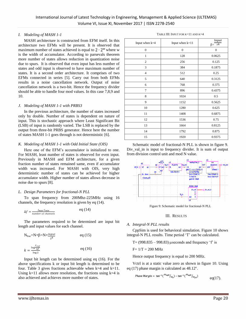
Schematic model of fractional-N PLL is shown in figure 9.
Div_val_in is input to frequency divider. It is sum of output
from division control unit and mod N value.
Figure 9: Schematic model for fractional-N PLL
III. RESULTS
A. Integral-N PLL results
CppSim is used for behavioral simulation. Figure 10 shows
integral-N PLL results. Time period „T‟ can be calculated.
T= (998.835 – 998.83) seconds and frequency „f‟ is
F= 1/T = 200 MHz
Hence output frequency is equal to 200 MHz.
Vctrl is at a static value zero as shown in figure 10. Using
eq (17) phase margin is calculated as 48.12.
eq(17).

International Journal of Latest Technology in Engineering, Management & Applied Science (IJLTEMAS)
Volume VI, Issue XI, November 2017 | ISSN 2278-2540
www.ijltemas.in Page 21
Figure 10: Integral-N PLL results
B. Analysis of Division Control Unit
Initially all four architectures of division control unit are
simulated for accumulator width k=4. An averaging function
is used to calculate the fractions. The resulting fractions for
corresponding inputs are shown in figure 11. It is observed
that for PRBS, absolute values are not achieved rather closer
values are achieved. LSB of input in MASH with PRBS is
dithered, hence when input seven is considered it essentially
dithers between six and seven. This is the reason average
observed is not expected value and for both six and seven
same average is observed. While EFM, MASH and MASH
with odd initial state achieves expected fractional values for
all inputs.
Figure 11: Comparing fractional values
The average output is equivalent to fraction n
input
2, where
n is the width of accumulator. It is also observed that number
of states are maximum for odd input while it varies for even
input. Figure 12, gives the following observations about
number of states for all inputs when bit length of input is four.
In EFM maximum number of states observed for inputs is 16.
For even inputs lesser number of states is observed and worst
case is 2. The number of states remains same for these
fractions even when the accumulator width is increased.
Maximum state for odd inputs at 32 and worst case
observed for even with four states. The number of states
remains same for these fractions even when the accumulator
width is increased.
MASH with Odd Initial State (OIS) improves minimum
number of states to eight. It also allows the fractions to
improve the number of states with increase in accumulator
width. Accumulator width of eleven is considered for
improving number of states. To achieve same fractions for
accumulator width of eleven, inputs need to be multiplied with
27. For all fractions when accumulator width is eleven, the
number of states observed is 2048. Where as in MASH
without odd initial state, number of states does not improve
when accumulator width is eleven. The improvement observed
is very high.
Figure 12: Comparing number of states when k=4
C. Fractional-N PLL results
The results of fractional-N PLL whose bandwidth is 1/10th
of reference frequency and MASH 1-1 divider modulator with
odd initial state is shown in figure 13. Input given is 896 which
implies that expected frequency is 210.9375 MHz. From figure
the freq_avg is approximately at 210.9375 MHz and jitter goes
up to 200 pico-seconds.
Figure 13:Fractional-N PLL results
International Journal of Latest Technology in Engineering, Management & Applied Science (IJLTEMAS)
Volume VI, Issue XI, November 2017 | ISSN 2278-2540
www.ijltemas.in Page 22
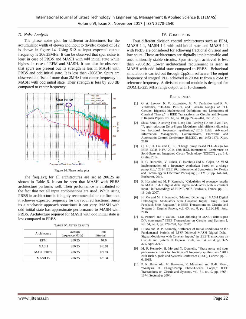
D. Noise Analysis
The phase noise plot for different architectures for the
accumulator width of eleven and input to divider control of 512
is shown in figure 14. Using 512 as input expected output
frequency is 206.25MHz. It can be observed that spur noise is
least in case of PRBS and MASH with odd initial state while
highest in case of EFM and MASH. It can also be observed
that spurs are present but its strength is less in MASH with
PRBS and odd initial state. It is less than -200dBc. Spurs are
observed at offset of more than 2MHz from center frequency in
MASH with odd initial state. Their strength is less by 200 dB
compared to center frequency.
Figure 14: Phase noise plot
The freq_avg for all architectures are set at 206.25 as
shown in Table 5. It can be seen that MASH with PRBS
architecture performs well. Their performance is attributed to
the fact that not all input combinations are used. While using
PRBS in architecture it is highly recommended to confirm that
it achieves expected frequency for the required fractions. Since
its a stochastic approach sometimes it can vary. MASH with
odd initial state has approximate performance to MASH with
PRBS. Architecture required for MASH with odd initial state is
less compared to PRBS.
TABLE IV: JITTER RESULTS
Architecture average
frequency(MHz)
rms
jitter(ps)
EFM 206.25 64.6
MASH 206.25 148.91
MASH PRBS 206.25 122.74
MASH IS 206.25 125.34
IV. CONCLUSION
Four different division control architectures such as EFM,
MASH 1-1, MASH 1-1 with odd initial state and MASH 1-1
with PRBS are considered for achieving fractional division and
low spurs. These architectures are digitally implementable and
unconditionally stable circuits. Spur strength achieved is less
than -200dBc. Lower architectural requirement is seen in
MASH with odd initial state compared to PRBS. Behavioral
simulation is carried out through CppSim software. The output
frequency of integral PLL achieved is 200MHz from a 25MHz
reference frequency. A division control module is designed for
200MHz-225 MHz range output with 16 channels.
REFERENCES
[1] G. A. Leonov, N. V. Kuznetsov, M. V. Yuldashev and R. V.
Yuldashev, "Hold-In, Pull-In, and Lock-In Ranges of PLL
Circuits: Rigorous Mathematical Definitions and Limitations of
Classical Theory," in IEEE Transactions on Circuits and Systems
I: Regular Papers, vol. 62, no. 10, pp. 2454-2464, Oct. 2015. [2] Shuai Zhou, Xiaoteng Fan, Liang Liu, Panfeng He and Jiwei Fan,
"A spur-reduction Delta-Sigma Modulator with efficient dithering
for fractional frequency synthesizer," 2016 IEEE Advanced
Information Management, Communicates, Electronic and
Automation Control Conference (IMCEC), pp. 1473-1476, Xi'an,
2016.
[3] Q. Lu, H. Liu and Q. Li, "Charge pump based PLL design for
IEEE 1394b PHY," 2014 12th IEEE International Conference on
Solid-State and Integrated Circuit Technology (ICSICT) , pp. 1-3,
Guilin, 2014. [4] R. G. Bozomitu, V. Cehan, C. Barabaşa and N. Cojan, "A VLSI
implementation of a frequency synthesizer based on a charge
pump PLL," 2014 IEEE 20th International Symposium for Design
and Technology in Electronic Packaging (SIITME) , pp. 141-144,
Bucharest, 2014. [5] K. Hosseini and M. P. Kennedy, “Calculation of sequence lengths
in MASH 1-1-1 digital delta sigma modulators with a constant
input,” in Proceedings of PRIME 2007, Bordeaux, France, pp. 13–
16, July 2007.
[6] H. Mo and M. P. Kennedy, "Masked Dithering of MASH Digital
Delta-Sigma Modulators with Constant Inputs Using Linear
Feedback Shift Registers," in IEEE Transactions on Circuits and
Systems I: Regular Papers, vol. 63, no. 8, pp. 1131-1141, Aug.
2016.
[7] S. Pamarti and I. Galton, “LSB dithering in MASH delta-sigma
D/A converters,” IEEE Transactions on Circuits and Systems I,
vol. 54, no. 4, pp. 779–790, Apr. 2007.
[8] H. Mo and M. P. Kennedy, "Influence of Initial Conditions on the
Fundamental Periods of LFSR-Dithered MASH Digital Delta–
Sigma Modulators with Constant Inputs," in IEEE Transactions on
Circuits and Systems II: Express Briefs, vol. 64, no. 4, pp. 372-
376, April 2017.
[9] M. P. Kennedy, H. Mo and Y. Donnelly, "Phase noise and spur
performance limits for fractional-N frequency synthesizers," 2015
26th Irish Signals and Systems Conference (ISSC), Carlow, pp. 1-
6, 2015.
[10] P. K. Hanumolu, M. Brownlee, K. Mayaram, and U.-K. Moon,
“Analysis of Charge-Pump Phase-Locked Loops,” IEEE
Transactions on Circuit and Systems, vol. 51, no. 9, pp. 1665–
1674, September 2004.