simulation and experimental verification of single-phase pwm … · · 2017-03-30single-phase...
TRANSCRIPT

International Research Journal of Engineering and Technology (IRJET) e-ISSN: 2395 -0056
Volume: 04 Issue: 03 | Mar -2017 www.irjet.net p-ISSN: 2395-0072
© 2017, IRJET | Impact Factor value: 5.181 | ISO 9001:2008 Certified Journal | Page 1689
Simulation and Experimental Verification of Single-Phase PWM Boost -
Rectifier with Controlled Power factor
M. A. Ahmed Ass. Professor, Electrical Engineering Department, Aljouf faculty of Engineering, Aljouf University, Kingdom of
Saudi Arabia
---------------------------------------------------------------------***---------------------------------------------------------------------Abstract - In this paper, a single-phase PWM boost rectifier operating at a controlled power factor has been simulated and implemented. The power circuit under investigation is a single-phase full bridge converter using IGBT transistors. The control algorithm provides the regulation of the output DC voltage as well as the control of supply current power factor. In addition, the proposed control strategy is implemented using a low-cost microcontroller Intel 80196. The experimental prototype offers several advantages such as; simplified control system, sinusoidal ac line current that satisfies the recently published harmonic current standard IEC 1000-3-2 Class D.
Key Words: Single Phase PWM rectifier, Controlled power factor, Hysterisis current controller, DC voltage regulation
1.INTRODUCTION
As the amount of equipment using conventional diode rectifiers increases, harmonic input currents are becoming a problem. Harmonic current limits are recommended by the IEC standards (IEC 1000-3-2). In an effort to meet these requirements, power-factor correction techniques to reduce harmonic current are becoming very important. Furthermore, it is desirable to have minimal size, high efficiency, and low electromagnetic interference [1]. The main disadvantages of classical rectifiers are: i) They generate a lagging displacement factor with respect to the utility voltage. ii) Increased total harmonic distortion (THD) of ac supply current. These aspects have a negative influence on both power factor and power quality. The IEC 1000-3-2 International Standard establishes limits to all low power single-phase equipment having an input current with a ‘‘special wave shape’’ and an active input power P ≤ 600W. Figure 1 shows the harmonic spectrum of a line current drawn by classical diode rectifier compared to the IEC 1000-3-2 standards. It is noted that the diode rectifier is not able to comply with the standard, because of the input current is highly distorted, and has a very low power factor due to its large harmonic content. Many research efforts have focused on the control of the harmonic emission from power electronics circuits. Harmonic control techniques such as: passive filtering, active filtering, and power factor correction have been used.
Fig -1: Harmonics spectrum of line current of diode
rectifier compared to IEC standard.
One problem associated with many existing drive systems with frequent regeneration is that the size of the dc link capacitor is often very large in order to limit the link voltage. Normally large capacitor bank of thousand micro-Farad is required, which increases the size, weight, and equipment cost. If braking resistor is used to dissipate the regenerative energy, the overall efficiency of the drive system becomes low [2-3]. The main features of PWM rectifier are: bi-directional power flow, nearly sinusoidal input current, regulation of input power factor to unity, low harmonic distortion of line current, adjustment and stabilization of DC link voltage, reduced capacitor due to bi-directional power flow [4-6].
2. THEORY AND OPERATION The power circuit of the fully controlled single-phase PWM rectifier in bridge connection, show in figure 2, uses four IGBT switches to provide a controlled DC voltage Vo. In this topology, the output voltage Vo must be higher than the peak value of the source voltage υs in order to ensure proper control of the input current [7].
Fig -2: Single-phase PWM rectifier

International Research Journal of Engineering and Technology (IRJET) e-ISSN: 2395 -0056
Volume: 04 Issue: 03 | Mar -2017 www.irjet.net p-ISSN: 2395-0072
© 2017, IRJET | Impact Factor value: 5.181 | ISO 9001:2008 Certified Journal | Page 1690
2.1 Modes of Operation
During positive half cycle, when S2, S3 are switched ON,
current is begins to flow through L, S2, C, S3, and returns to
the mains with polarity shown in figure 3.a. The inductor
voltage has the following expression;
)( veVdt
diL os
sL (1)
which means an increase in the instantaneous value of the
input current is.
Fig -3: Equivalent circuit of PWM rectifier, (a) when S2, S3
ON, (b) when S2, S3 OFF.
When S2, S3 are switched OFF (to decrease is): the polarity
of inductor voltage is reversed, making diode D1, D4
conducts and current is begins to charge capacitor C
through the inductor L, and diodes D1, D4 and permits the
rectifier to produce dc power, then returns to the mains
with the polarity shown in figure 3.b.
In this condition, the inductor voltage is given by;
)( veVdt
diL os
sL (2)
therefore, a decrease in the input current is occurs.
During negative half cycle, a similar operation occurs but
with S1, S4 and D2, D3.
The mathematical model of single phase PWM rectifier
may be represented by means of figure 4.
Fig -4: Single line representation of the PWM rectifier.
The converter voltage could be represented as follows:
conv
ss V
dt
diL (3)
)(1
convss V
Ldt
di (4)
Assume the load is pure resistive, the dc current could be
represented as:
)(1
o
odc
o
o
oodc
oCdc
R
VI
Cdt
dV
R
V
dt
dVCI
III
Currents and voltages can be represented as function of switching states as follows:
Idc = (S1 – S3 ) is (10)
oconv VSSV )( 31 (11)
where υs is the ac supply voltage, is is ac supply the current,
Vconv is the converter voltage, Vo is the dc output voltage, Io is
the dc output current, Ro is the load resistance, and S1, S2,
S3, S4 are the switching states of IGBT transistors.
3. PROPOSED CONTROL STRETEGY
Figure 5 presents the block diagram of the proposed control
algorithm of PWM rectifier.
Fig -5: Block diagram of implemented control strategy.
The voltage source rectifier operates by keeping the DC-link
voltage at a desired reference value, using a feedback control
loop. To accomplish this task, the dc link voltage is measured
and compared with a reference Vref. The error signal is
applied to PI controller then multiplied by a unity sin. The
resulting signal is considered to be the reference current,
which is compared to the actual source current and
producing the switching pattern through a hysteresis
controller. The signal generated from this comparison is used
to ON and OFF the four switches of the rectifier. In this way,
power can come or return to the ac source according to dc
link voltage requirements. When the current Io is positive
(rectifier operation), the capacitor C is discharged, and the
error signal ask the control block for more power from the ac
supply. The control block takes the power from the supply by
generating the appropriate PWM signals for the four
switches. In this way, more current flows from the ac to the
dc side, and the capacitor voltage is recovered. Inversely,
when Io becomes negative (inverter operation), the capacitor
C is overcharged, and the error signal asks the control to
discharge the capacitor and return power to the ac mains.
Figure 6 shows the waveforms and phasor diagrams for PWM
rectifier at unity, leading, and lagging power factor
operations.
(a)
(b)
(5)
(6)
(7)

International Research Journal of Engineering and Technology (IRJET) e-ISSN: 2395 -0056
Volume: 04 Issue: 03 | Mar -2017 www.irjet.net p-ISSN: 2395-0072
© 2017, IRJET | Impact Factor value: 5.181 | ISO 9001:2008 Certified Journal | Page 1691
Fig -6: Operation of PWM rectifier. (a) operation at unity power factor. (b) operation at leading power factor.
(c) operation at lagging power factor.
4. SIMULATION RESUTS
A simulation platform using Simulink and Power System Block Set under MATLAB is built to evaluate the performance under different operating conditions. The system parameters are shown in Table 1. The step time of solution is 100μsec, which is equivalent to 10KHz sampling rate.
Table -1: System Parameters. Parameter Value
AC supply voltage 40Vrms
Line inductor 10mH
Load resistance 100Ω
DC link capacitor 1mF
Hysteresis band 2%
Figure 7 presents the ac source current of classical diode rectifier, which is highly distorted waveform.
Fig -7: AC line current of diode rectifier
Figure 8 presents the steady state performance at unity power factor operation. The dc load voltage is regulated at 140V. The ac source current has a high-quality waveform.
0.1 0.12 0.14 0.16 0.18 0.2
-50
0
50
100
150
Vs
Is*2
Vdc
Vr
Fig -8: Steady state performance at unity power factor.
Figure 9 shows the transient response according to lead-lag power factor operation with angle of 30o.
0.04 0.06 0.08 0.1 0.12 0.14 0.16
-50
0
50
100
150
200
Vs
Is*2
Vdc
Vr
Fig -9: Transient response due to lead-lag power factor.
Figure 10 shows the transient response according to step change in reference load voltage form 140V to 160V.
Fig -10: Transient response due to step change in reference load voltage.
t [sec]
V[V]
I [A]
V[V] I [A]
V[V] I [A]
t [sec]
V[V] I [A]
t [sec]
International Research Journal of Engineering and Technology (IRJET) e-ISSN: 2395 -0056
Volume: 04 Issue: 03 | Mar -2017 www.irjet.net p-ISSN: 2395-0072
© 2017, IRJET | Impact Factor value: 5.181 | ISO 9001:2008 Certified Journal | Page 1692
5. EXPERIMENTAL SETUP
Figure 11 presents the block diagram of the implemented system. Principle connections between the different elements in the complete system are indicated. The software algorithm was implemented using an Intel 80C196KC 16-bit embedded microprocessor.
Fig -11: Block diagram of the implemented system
This microcontroller provides an A/D converter with multiplexed eight-input channels, which is used for the various A/D operations required by the controller algorithm. The output ports provided by the 80196 are used for interfacing the switching signals to the IGBT drivers. The high-speed input port is used for line voltage zero-crossing detection measurement [8]. The system parameters are shown in Table 1 with a hysteresis band of 2%. In all experimental results the sampling rate of data of microcontroller card is 9KHz. Figure 12 shows the waveform of the ac source current and the ac line voltage of single-phase diode rectifier. As plotted in figure the source current has a low-quality waveform.
Fig -12: Source current of diode bridge rectifier.
2A/div., 30V/div.
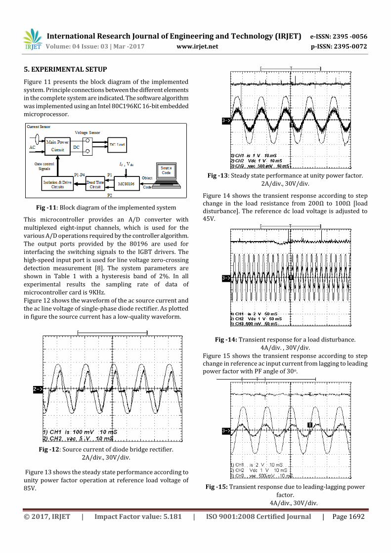
Figure 13 shows the steady state performance according to unity power factor operation at reference load voltage of 85V.
Fig -13: Steady state performance at unity power factor.
2A/div., 30V/div.
Figure 14 shows the transient response according to step change in the load resistance from 200Ω to 100Ω [load disturbance]. The reference dc load voltage is adjusted to 45V.
Fig -14: Transient response for a load disturbance. 4A/div. , 30V/div.
Figure 15 shows the transient response according to step change in reference ac input current from lagging to leading power factor with PF angle of 30o.
Fig -15: Transient response due to leading-lagging power
factor. 4A/div., 30V/div.

International Research Journal of Engineering and Technology (IRJET) e-ISSN: 2395 -0056
Volume: 04 Issue: 03 | Mar -2017 www.irjet.net p-ISSN: 2395-0072
© 2017, IRJET | Impact Factor value: 5.181 | ISO 9001:2008 Certified Journal | Page 1693
6. CONCLUSION
In this paper a high performance single phase PWM boost rectifier has been implemented using IGBT transistors as a power switch. The mathematical model and the experimental verification are presented. The control algorithm of experimental prototype is implemented using a single chip Intel Microcontroller 80196KC. The software source codes are elaborated in assembly language directly. The experimental results prove that the converter draws a near sinusoidal current waveform with low THD. Moreover, the converter can operate at any desired power factor (lead, unity, and lag). The dc load voltage is regulated against load disturbance and variation. The maximum obtainable sampling frequency is 9 KHz, which resulted in an actual switching frequency of about 2.6 KHz.
REFERENCES
[1] Jee-Woo Lim and Bong-Hwan Kwon “A Power-Factor Controller for Single-Phase PWM Rectifiers,” IEEE Transaction on industrial electronics, vol. 46, no. 5, pp. 1035-1037, October 1999. DOI: 10.1109/41.793353
[2] S. Y. (Ron) Hui, Henry Shu-Hung Chung “A Bidirectional AC-DC Power Converter with Power Factor Correction,” IEEE Transactions on power electronics vol. 15, no. 5, pp. 942-948, September 2000. DOI: 10.1109/63.867684
[3] Dharmesh D. Prajapati; Mihir B. Chaudhari, “Power Factor Correction of Single Phase PWM boost Rectifier”, 2015 International Conference on Electrical, Electronics, Signals, Communication and Optimization (EESCO), pp. 1-4, 2015. DOI: 10.1109/EESCO.2015.7253903.
[4] Y. Konishi; Y. Matsumoto; P. Boyagoda; M. Nakaoka, “Current-fed three-phase rectifier with optimum PWM-based sinewave line current shaping and unity power factor correction schemes,” Industrial Electronics, Control and Instrumentation, 1997. IECON 97. 23rd International Conference, 1997, Vol. 2, pp. 888 – 894, DOI: 10.1109/IECON.1997.672080.
[5] Ohnishi “Three phase PWM converter/inverter by means of active and reactive power control,” In Proc. IEEE IECON, 1991, vol.1, pp. 819-824. DOI: 10.1109/IECON.1991.239183.
[6] T. Noguchi, H. Tomiki, S. Kondo, and I. Takahashi “Direct power control of PWM Converter without Power Source Voltage Sensors,” IEEE Trans. On Industry Applications, vol.34, no.3, pp. 473-479, May/June 1998. DOI: 10.1109/28.673716
[7] N. Mohan, T.M. Undeland and W.P. Robbins, Power Electronics: Converters, Applications and Design, John Wiley & Sons, 1989, pp.425-426.
[8] Bong- Hwan Kown and Byung-duk Min “A Fully Software-Controlled PWM Rectifier with Current Link,” IEEE Transaction on industrial electronics, vol. 40, no. 3, June 1993. DOI: 10.1109/41.232215
BIOGRAPHIES
Mohamed Adel Ahmed was born in Cairo, Egypt in 1978. He received his B.S. and M.S. in Electrical Engineering from Benha University, Egypt, in 2000 and 2006, respectively, and his Ph.D. in Electrical Engineering from Cairo University, Egypt, in 2011. Since 2002 to 2014, he has been with the Department of Electrical
Engineering and Technology, Faculty of Engineering, Banha University. From 2014 till now he is Ass. Prof. in Department of Electrical Engineering, Aljouf Faculty of Engineering, Aljouf University