simulation and experimental study of photogeneration and recombination in amorphous-like
TRANSCRIPT
Hindawi Publishing CorporationInternational Journal of PhotoenergyVolume 2013, Article ID 698026, 6 pageshttp://dx.doi.org/10.1155/2013/698026
Research ArticleSimulation and Experimental Study ofPhotogeneration and Recombination in Amorphous-Like SiliconThin Films Deposited by 27.12 MHz Plasma-Enhanced ChemicalVapor Deposition
Chia-Hsun Hsu,1 In-Cha Hsieh,1 Chia-Chi Tsou,2 and Shui-Yang Lien2
1 Graduate Institute of Precision Engineering, National Chung Hsing University, Taichung 402, Taiwan2Department of Materials Science and Engineering, MingDao University, Changhua 52345, Taiwan
Correspondence should be addressed to Shui-Yang Lien; [email protected]
Received 22 November 2012; Revised 3 May 2013; Accepted 16 May 2013
Academic Editor: Peter Rupnowski
Copyright © 2013 Chia-Hsun Hsu et al.This is an open access article distributed under the Creative CommonsAttribution License,which permits unrestricted use, distribution, and reproduction in any medium, provided the original work is properly cited.
Amorphous-like silicon (a-Si:H-like) thin films are prepared by 27.12MHz plasma-enhanced chemical vapor deposition technique.The films are applied to p-i-n single junction thin film solar cells with varying i-layer thickness to observe the effects on the short-circuit current density, as well as the open-circuit voltage, fill factor, and conversion efficiency. The most significant experimentalresult is that 𝐽sc has two different behaviors with increasing the i-layer thickness, which can be related to carrier collection efficiencyin the long wavelength region. Furthermore, technology computer-aided design simulation software is used to gain better insightinto carrier generation and recombination of the solar cells, showing that for the i-layer thickness of 200 to 300 nm the generationdominates the carrier density and thus 𝐽sc, whereas for the i-layer thickness of 300 to 400 nm the recombination becomes the leadingfactor.The simulation results of cell performances are in good agreement with experimental data, indicating that our simulation hasgreat reliability. In addition, the a-Si:H-like solar cells have low light-induced degradation, which in turn can have a great potentialto be used for stable and high-efficiency solar cells.
1. Introduction
Hydrogenated amorphous silicon (a-Si:H) thin films havebeen widely studied in photovoltaic technology in recentyears. Because of a high-absorption coefficient of a-Si:H in thevisible range of the solar spectrum, 1𝜇m thick a-Si:H layer isenough to absorb 90% of usable solar energy. However, largedeviations in bonding angles and bonding lengths betweenthe neighboring atoms in a-Si:H result in the weak or strainedbonds, which would easily break and thus form defects inthe atomic network. As a result, a-Si:H suffers from thephotoinduced problem of degradation, known as Stabler-Wronski effect, which reduces the efficiency of solar cells afterlight illumination. One alternative is the use of hydrogenatedmicrocrystalline silicon (𝜇c-Si:H), in which small crystals ofhighly ordered material in the range of tenths of nanometers
are embedded. The amplitude of the degradation is a func-tion of the crystallinity of the 𝜇c-Si:H layer: the lower thecrystallinity, the higher the light-induced degradation. It isdemonstrated more precisely that light-induced degradationis proportional to the ratio of the amorphous volume overthe crystalline volume [1, 2]. For solar cell applications the𝜇c-Si:H absorber is typically larger than 1 𝜇m representing anincrease in production time and thus fabrication cost [3].
Recently a-Si:H-like materials, intermediate between a-Si:H and 𝜇c-Si:H, have been deposited [4, 5]. The filmsconsist of silicon crystallites and/or clusters (less than 3 nm)which is difficult to be observed from the morphology ofthe films. Further, a-Si:H-like films have the same opticalabsorption coefficient as a-Si:H but the improved transportproperties of 𝜇c-Si:H. In particular, the quantum efficiency-mobility-lifetime (𝜂𝜇𝜏) product of electrons can be a factor of
2 International Journal of Photoenergy
Table 1: Deposition conditions of the intrinsic and doped a-Si:H-like layers.
Deposition condition p-typea-SiC:H
Bufferlayer
Intrinsiclayer
n-typelayer
Power (W) 10 10 10 10Pressure (Pa) 90 90 90 60E/S (mm) 20 20 30 25Temperature (∘C) 200 200 200 200SiH4 flow rate (sccm) 20 20 40 40H2 flow rate (sccm) 40 40 160 80CH4 flow rate (sccm) 18 18 — —B2H6 flow rate (sccm) 5 — — —PH3 flow rate (sccm) — — — 5Layer thickness (nm) 10 6 200–400 30
100 higher than that of typical a-Si:H in the as-deposited state,while 𝜂𝜇𝜏 product values after light soaking are comparableto typical a-Si:H before degradation [6–8]. Furthermore, thevalues of the deep defect density estimated from an analysisof modulated photocurrent (MPC) are about 10 times lowerthan those of typical a-Si:H [9]. Although the basic propertiesof a-Si:H-like films have been proposed, the application insolar cell research is not well investigated [6–12].
In this study, we apply the a-Si:H-like films to fabricatep-i-n single junction solar cells and vary the i-layer thick-ness from 200 to 400 nm. Effects of the i-layer thicknesson the device performances such as open-circuit voltage(𝑉oc), short-circuit current density (𝐽sc), fill factor (FF), andconversion efficiency (𝜂) are investigated. We use 27.12MHzhigh-frequency plasma-enhanced chemical vapor deposition(HF-PECVD) to deposit silicon thin films, and the filmsalmost always contain small crystalline fractions even underlow H
2/SiH4gas ratios. This kind of a-Si:H-like films could
also be obtained by 13.56MHz radio frequency PECVD butusually requiring a high H
2/SiH4ratio which might dra-
matically decrease the deposition rate. Moreover, technologycomputer-aided design simulation software (TCAD) is usedto gain better insight into charge carrier generation andrecombination of the devices.
2. Experimental
Thea-Si:H-like single junction thin film solar cells were fabri-cated with structure of Asahi SnO
2:F-coated glass/p/buffer/i/
n/ZnO:Al/Ag. All of the Si layers were prepared by HF-PECVD at a frequency of 27.12MHz. Diborane (B
2H6) and
phosphine (PH3) gases were used as the doping gas to
fabricate the a-Si:H-like p- and n-layers. To reduce the bandoffset between the energy bands of a wide band-gap p-type SiC (1.9 eV) and intrinsic layers, a buffer layer wasused at the p/i interface [13, 14]. The detailed depositionconditions are summarized in Table 1. Five single junctionsolar cells were fabricated, and the i-layer thickness wasvaried from 200 to 400 nm. The electrical, optical, andstructural properties of the i-layer a-Si:H-like films are listed
Table 2: The properties of a-Si:H-like films compared to those oftypical a-Si:H films.
a-Si:H a-Si:H-likeCrystallinity (%) — 12Dark conductivity (Ω−1 cm−1) 1 × 10⁻¹⁰ 2.3 × 10⁻¹⁰
Photo conductivity (Ω−1 cm−1) 1 × 10⁻⁵ 6.1 × 10⁻⁴
Defect density (cm−3) ∼1016 1015
Hydrogen content (at.%) 15 10Absorptivity at 400 nm (cm−1) 5 × 10⁵ 1.3 × 10⁶
Absorptivity at 600 nm (cm−1) 3.5 × 10⁴ 7.5 × 10⁴
Activation energy (eV) 0.8 0.76Band gap (eV) 1.8 1.67
in Table 2 in comparison with a-Si:H. In Table 2, the values ofthe left column (a-Si:H) were obtained from [15]. The valuesof the right column (a-Si:H-like) were measured from ourexperimental films.The crystallinity was evaluated by micro-Raman spectroscopy.The dark conductivity was measured atroom temperature using a source-measure unit (KEITHLEY2400). The photoconductivity measurement was carried outunder AM1.5G (100mW/cm2) of a solar simulator.The defectdensity was obtained by electron spin resonance (ESR).The bonded hydrogen content was determined by Fouriertransform infrared (FTIR) spectroscopy.The absorptivitywasobtained bymeans ofUV-VIS spectrophotometer.The activa-tion energywas calculated from temperature-dependent darkconductivity measurements. The band gap was estimatedby a linear fit to a Tauc plot. The area of individual solarcells was defined by the 1 × 1 cm2 sputtered ZnO:Al/Agback contact. The film thickness was determined using analpha-step profilometer. The solar cells were characterizedby current density-voltage (𝐽-𝑉) measurement under 1-sun(AM1.5G, 100mW/cm2) solar simulator irradiation and spec-tral response measurement from which external quantumefficiency (EQE) was obtained. The 1-sun standard lightsoaking test was performed in a climate chamber at 50∘C for500 h (IEC 61646).
To simulate thin film solar cells the commercially avail-able software Silvaco TCAD, from Silvaco Inc., was used.The simulation program solved the Poisson equation coupledwith the continuity equations of electrons and holes for thevirtual device by dividing the whole structure into finiteelements. The physical models that we used were Shockley-Read-Hall recombination model, concentration-dependentlifetimes, and low field mobility model. The photogener-ation model, including a ray tracing algorithm, was usedto calculate the absorption and transmission of light inthe semiconductor layers. The solar cells considered hereoperate under the global standard solar spectrum (AM1.5G)illumination with 100mW/cm2 total incident power density.Table 3 lists the minimum set of input optical, electrical,and structural parameters used in this simulation withoutbuffer layers between each layer. The theoretical values ofthe band mobility for a-Si:H-based thin films were around 1–10 cm2s−1V−1. The hole mobility was assumed to be smallerthan the electron mobility. The i-layer thickness varied
International Journal of Photoenergy 3
Table 3: The minimum set of input parameters used in oursimulation work.
Device parameter ValueDevice area (um2) 1Average haze (%) 18Exterior rear reflectance (%) 95Light source One sun (AM 1.5, 100mW/cm2)Layer parameters p-layer i-layer n-layerThickness (nm) 10 200–400 10Doping concentration (cm−3) 1 × 10¹⁸ 1 × 10¹⁰ 1 × 10¹⁹
Mobility gap (eV) 1.92 1.67 1.7Electron mobility (cm2/Vs) 8 4 8Hole mobility (cm2/Vs) 2 0.7 2Effective DOS in CB (cm−3) 2.0 × 10²⁰ 2.0 × 10²⁰ 2.0 × 10²⁰
Effective DOS in VB (cm−3) 2.0 × 10²⁰ 2.0 × 10²⁰ 2.0 × 10²⁰
Dielectric constant 11.9 11.9 11.9Electron affinity (eV) 3.9 4 4Tail state (cm−3) 1020 1020 1020
Gaussian-state (cm−3) 5 × 10¹⁶ 5 × 10¹⁶ 5 × 10¹⁶
between 200 and 400 nm, while both p- and n-layers werefixed to 10 nm, 30 nm, respectively. The average haze was setto be 18% for the device constructed with rough texturedsurfaces between layers. The distribution of states in theenergy gap of a-Si:H assumed in the simulation is the generalstandard model of density of states (DOS), having twoexponential band tails and twoGaussian distribution of statesin the mobility gap [15, 16].
3. Results and Discussion
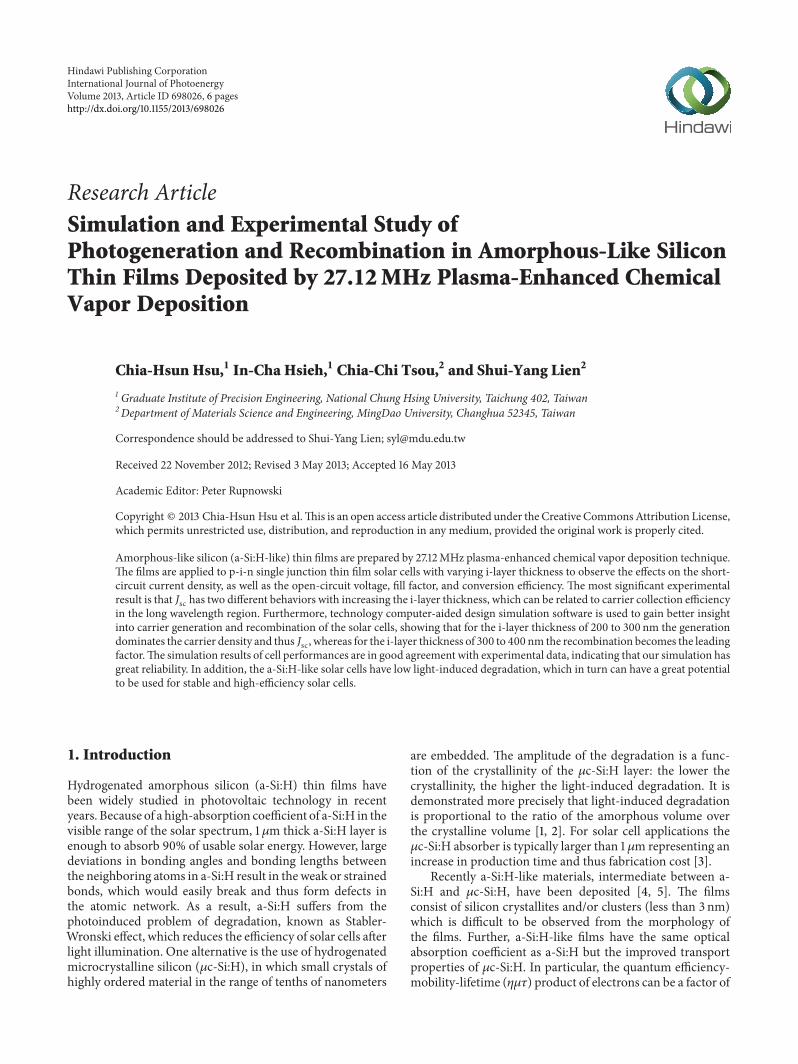
For each i-layer thickness, twenty solar cells were fabricatedand they had very similar performances (error less than 5%).Figure 1 is a representative result of 𝐼-𝑉 curves of solar cellswith different a-Si:H-like i-layer thickness. It can be seen thatthe cell with a 300 nm i-layer has the highest 𝐽sc value of17mA/cm2, while the other cells show 𝐽sc values around 15.5–16mA/cm2. Only little variation in 𝑉oc is seen, and this mayagree to that 𝑉oc would rather be affected by the qualitiesof thin film and p/i interface [17, 18]. From this result, thebest combination of 𝑉oc and 𝐽sc can be found for an i-layerthickness of 300 nm.
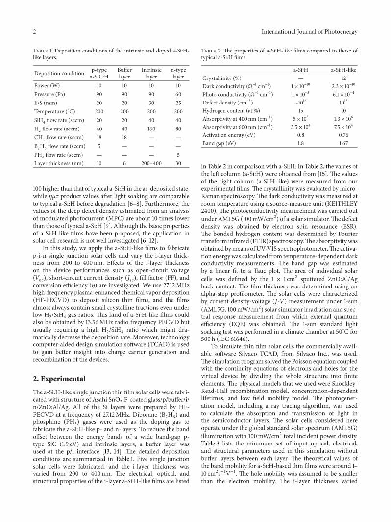
Figure 2 shows the EQE of the cells with different a-Si:H-like i-layer thickness. The result is helpful to evaluatethe carrier collection efficiency at a particular wavelength.It is found that the curves remain the same in the short-wavelength region (<500 nm) for each i-layer thickness dueto the good performances of the p-doped layer [19]. But thecurves vary in the long-wavelength region (>500 nm) withtheir peaks red-shifting. At the wavelength of 600 nm, theEQE values for the thickness of 200–400 nm are 61%, 65%,69%, 68%, and 63%, respectively. It is interesting to clarifythat the EQE differences in the long-wavelength regionmightresult from the thickness variation rather than the crystallinefractions in the a-Si:H-like films. This can also be evidenced
0
3
6
9
12
15
18
0 0.2 0.4 0.6 0.8 1Voltage (V)
Curr
ent d
ensit
y (m
A/c
m2)
200 nm250 nm300 nm
350 nm400 nm
Figure 1: Experimental 𝐼-𝑉 characteristics of a-Si:H-like solar cellswith different i-layer thickness.
0
10
20
30
40
50
60
70
80
90
100
300 400 500 600 700 800 900Wavelength (nm)
EQE
(%)
200 nm250 nm300 nm
350 nm400 nm
Figure 2: Experimental quantum efficiencies of a-Si:H-like solarcells with different i-layer thickness.
by the observation that the cutoff wavelength of each cell isabout 800 nm, same as that of a-Si:H.
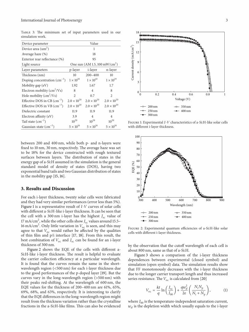
Figure 3 shows a comparison of the i-layer thicknessdependences between experimental (closed symbol) andsimulation (open symbol) data. The simulation results showthat FF monotonously decreases with the i-layer thicknessdue to the longer carrier transport length and thus increasedseries resistance. The 𝑉oc is calculated from [20]
𝑉oc =𝑘𝑡
𝑞ln(
𝐽sc𝐽00
) +𝑞𝑤2
𝑑
2𝜀(
𝑁i𝑁p
𝑁i + 𝑁p) , (1)
where 𝐽00is the temperature-independent saturation current,
𝑤𝑑is the depletion width which usually equals to the i-layer
4 International Journal of Photoenergy
14.5
15.5
16.5
17.5
18.5
0.73
0.77
0.81
0.85
0.89
0.93
0.68
0.70
0.72
0.74
0.76
0.78
0.80
8
9
10
11
12
13
150 200 250 300 350 400 450i-layer thickness (nm)
𝜂(%
)FF
Voc
(V)
J sc
(mA
/cm
2)
Figure 3: Simulated (open symbol) and experimental (closedsymbol) results of external parameters of a-Si:H-like solar cells withdifferent i-layer thickness.
thickness for a p-i-n device, and 𝑁i and 𝑁p are the majoritycarrier concentration in the i-layer and in the p-layer, respec-tively. The last part of the equation is the built-in voltageacross the i-layer.Therefore,𝑉oc would vary depending on thevalues of𝑤
𝑑and 𝐽sc. For the i-layer thickness of 300–400 nm,
the loss in 𝑉oc caused by the decreased 𝐽sc is compensated bythe increased 𝑤
𝑑. Finally, the trend of 𝜂 is similar to that of
𝐽sc implying that the cell efficiency is mainly dominated by𝐽sc. Overall, the trends of the simulation results match wellwith that of experimental ones.
0 0.1 0.2 0.3 0.4
Generation rateRec. 200 nmRec. 250 nm
Rec. 300 nmRec. 350 nmRec. 400 nm
1022
1021
1020
1019
1018
1017
1016
1015
x (𝜇m)
g,r
(cm
−3s−
1)
Figure 4: Simulated carrier generation rate and recombination rateas a function of the i-layer thickness.
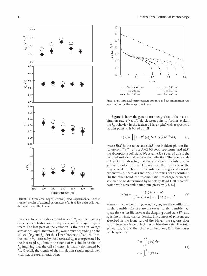
Figure 4 shows the generation rate, 𝑔(𝑥), and the recom-bination rate, 𝑟(𝑥), of hole-electron pairs to further explainthe 𝐽sc behavior. In the textured i-layer, 𝑔(𝑥)with respect to acertain point, 𝑥, is based on [21]
𝑔 (𝑥) = ∫ [1 − 𝑅2
(𝜆)] 𝑆 (𝜆) 𝛼 (𝜆) 𝑒−𝛼𝑥
𝑑𝜆, (2)
where 𝑅(𝜆) is the reflectance, 𝑆(𝜆) the incident photon flux(photon cm−2s−1) of the AM1.5G solar spectrum, and 𝛼(𝜆)
the absorption coefficient. We assume 𝑅 is squared due to thetextured surface that reduces the reflection. The 𝑦-axis scaleis logarithmic showing that there is an enormously greatergeneration of electron-hole pairs near the front side of thei-layer, while further into the solar cell the generation rateexponentially decreases and finally becomes nearly constant.On the other hand, the recombination of charge carriers isassumed to be determined by Shockley-Read-Hall recombi-nation with a recombination rate given by [22, 23]
𝑟 (𝑥) =𝑛 (𝑥) 𝑝 (𝑥) − 𝑛
2
i𝜏p [𝑛 (𝑥) + 𝑛i] + 𝜏n [𝑝 (𝑥) + 𝑛i]
, (3)
where 𝑛 = 𝑛0+ Δ𝑛, 𝑝 = 𝑝
0+ Δ𝑝, 𝑛
0, 𝑝0are the equilibrium
carrier densities, Δ𝑛, Δ𝑝 are the excess carrier densities, 𝜏n,𝜏p are the carrier lifetimes at the dangling bond state𝐷0, and𝑛i is the intrinsic carrier density. Since most of photons areabsorbed in the front part of the i-layer, the regions closeto p/i interface have a high recombination rate. The totalgeneration, 𝐺, and the total recombination, 𝑅, in the i-layercan be given by
𝐺 = ∫
𝑑
0
𝑔 (𝑥) 𝑑𝑥,
𝑅 = ∫
𝑑
0
𝑟 (𝑥) 𝑑𝑥.
(4)

International Journal of Photoenergy 5
0 0.1 0.2 0.3 0.4 0.5 0.6 0.7 0.8
x (𝜇m)
8
9
10
11
12
13
14
0.5
1
1.5
0 0.2 0.4 0.6 0.8
G
R
x (𝜇m)
G,R
(×1020
cm−2s−
1)
Nne
t(×1020
cm−2s−
1)
Figure 5: The total generation and recombination of solar cellswith different i-layer thickness. The inset of Figure 6 shows thecalculation result of the net charge carrier density for each i-layerthickness.
Note that the integral should be extended only from 𝑥 = 0
to the value of corresponding thickness, 𝑑. The calculationresults are plotted in Figure 5. The total generation increasesrapidly with the i-layer thickness, and a saturation occurssince the contribution at the deeper region of the i-layer canbe neglected.Therefore, it is easy to obtain the net free carrierconcentration,𝑁net, as given by
𝑁net = 𝐺 − 𝑅. (5)
The calculation result of 𝑁net is illustrated as an inset inFigure 5.The trend is consistentwith that of 𝐽sc observed fromthe experimental 𝐼-𝑉 measurement. However, 𝑁net wouldfinally be a constant indicating that 𝐽sc would still saturateafter a temporary decrease. It is interesting that if the textureis not considered, the saturation of the generation will shiftto the thick region. As a consequence, 𝑁net simply increasesand then saturates without having a decrease.
Figure 6 shows the conversion efficiencies of the cells after500 h exposure to 100mW/cm2 AM1.5G light for differenti-layer thickness. It can be seen that degradation increasesfrom 8.39% to 16.96% as i-layer thickness increases. The i-layer thickness of 300 nm shows the best stabilized efficiencyof 9% and a degradation of 11% smaller than the typicalvalue (>15%) observed from a-Si:H solar cells. The 200 nmand 250 nm thick i-layers show lower initial efficiencies of9.65% and 9.88%, respectively, but their stabilized efficienciesare close to that of the 300 nm thick i-layer. Degradation inthe cells with the 350 and 400 nm thick i-layer are about13.2% and 16.9%, respectively. Apparently, the thicker cellshave a higher degradation, and this might be attributed totwo reasons. First, a thick absorber leads to a weak electricfield, which in turn decreases the carrier collection efficiency.Second, the total amount of the light-induced defects causedby the hydrogen out-diffusion from Si–H bonds is larger
8
8.5
9
9.5
10
10.5
0 100 200 300 400 500
i-layer(nm)
Initial Stabilized Degradation
200 9.65 8.84 8.4250 9.88 8.93 9.64300 10.11 8.99 11.1350 9.74 8.45 13.2400 9.67 8.03 16.9
Light soaking time (hr)
Con
vers
ion
effici
ency
(%)
200 nm250 nm300 nm
350 nm400 nm
(%)(%)(%)
Figure 6: Light soaking effect for solar cells with different i-layerthickness.
for thicker absorbers. These defects will further flatten theelectric field and thus increase the degradation.
4. Conclusions
In conclusion, the a-Si:H-like films deposited by 27.12MHzPECVD have been applied to p-i-n single junction solar cellsto investigate the influences on photovoltaic performances.The TCAD simulation result is in good agreement withthe experimental data, showing great reliability. The carriergeneration and recombination profiles are shown to explainthe 𝐽sc behavior.The generation dominates the device currentdensity when the thin absorber is used, while for the thickerabsorber the recombination begins to offset the current gainand results in a temporary reduction in 𝐽sc. The i-layerthickness of 300 nm can have the optimum balance betweenthe generation and the recombination.The solar cell with the300 nm i-layer also has a comparable initial efficiency and alow degradation compared to that of a-Si:H cells. As a result,the thin absorber and good stability make the a-Si:H-likematerial suitable for solar applications.
Acknowledgments
This work is sponsored by the BeyondPV Company and theNational Science Council of the Republic of China underContract nos. 100-2622-E-451-001-CC2, 100-2628-E-451-002-MY2, and 101-3113-E-451-001-CC2.
References
[1] F. Finger, R. Carius, T. Dylla, S. Klein, S. Okur, and M. Gunes,“Stability of microcrystalline silicon for thin film solar cellapplications,” IEE Proceedings, vol. 150, no. 4, pp. 300–308, 2003.
[2] Y. Wang, X. Geng, H. Stiebig, and F. Finger, “Stability of micro-crystalline silicon solar cells with HWCVD buffer layer,” ThinSolid Films, vol. 516, no. 5, pp. 733–735, 2008.

6 International Journal of Photoenergy
[3] O. Vetterl, A. Lambertz, A. Dasgupta et al., “Thickness depen-dence of microcrystalline silicon solar cell properties,” SolarEnergy Materials and Solar Cells, vol. 66, no. 1–4, pp. 345–351,2001.
[4] P. Roca i Cabarrocas, S. Hamma, S. N. Sharma, J. Costa, and E.Bertran, “Nanoparticle formation in low-pressure silane plas-mas: bridging the gap between a-Si:H and 𝜇c-Si films,” Journalof Non-Crystalline Solids, vol. 227–230, no. 2, pp. 871–875, 1998.
[5] A. Fontcuberta IMorral, R. Brenot, E. A. G.Hamers, R. Vander-haghen, and P. Roca i Cabarrocas, “In situ investigation of poly-morphous silicon deposition,” Journal of Non-Crystalline Solids,vol. 266-269, pp. 48–53, 2000.
[6] P. Roca i Cabarrocas, A. Fontcuberta i Morral, S. Lebib, andY. Poissant, “Plasma production of nanocrystalline siliconparticles and polymorphous silicon thin films for large-areaelectronic devices,” Pure and Applied Chemistry, vol. 74, no. 3,pp. 359–367, 2002.
[7] P. St’ahel, S. Hamma, P. Sladek, and P. Roca i Cabarrocas, “Meta-stability studies in silicon thin films: from short range orderedto medium and long range ordered materials,” Journal of Non-Crystalline Solids, vol. 227, part 1, pp. 276–280, 1998.
[8] P. Roca i Cabarrocas, “Plasma deposition of silicon clusters: away to produce silicon thin films with medium-range order?”Materials Research Society Symposium, vol. 507, p. 855, 1998.
[9] C. Longeaud, J. P. Kleider, P. Roca i Cabarrocas, S. Hamma, R.Meaudre, and M. Meaudre, “Properties of a new a-Si:H-likematerial: hydrogenated polymorphous silicon,” Journal of Non-Crystalline Solids, vol. 227-230, no. 1, pp. 96–99, 1998.
[10] A. Fontcuberta i Morral, R. Brenot, E. A. G. Hamers, R.Vanderhaghen, and P. Roca i Cabarrocas, “In situ investigationof polymorphous silicon deposition,” Journal of Non-CrystallineSolids, vol. 266-269, pp. 48–53, 2000.
[11] K. H. Kim, E. V. Johnson, and P. Roca i Cabarrocas, “Irreversiblelight-induced degradation and stabilization of hydrogenatedpolymorphous silicon solar cells,” Solar Energy Materials andSolar Cells, vol. 105, pp. 208–212, 2012.
[12] Y. Poissant, P. Chatterjee, and P. Roca i Cabarrocas, “No benefitfrom microcrystalline silicon N layers in single junction amor-phous silicon p-i-n solar cells,” Journal of Applied Physics, vol.93, no. 1, pp. 170–174, 2003.
[13] B. Rech, C. Beneking, and H. Wagner, “Improvement in sta-bilized efficiency of a-Si:H solar cells through optimized p/i-interface layers,” Solar Energy Materials and Solar Cells, vol. 41,pp. 475–483, 1996.
[14] S. N. Agbo, J. Krc, R. A. C. M. M. Van Swaaij, and M. Zeman,“Optimization of the pi interface properties in thin film micro-crystalline silicon solar cell,” Solar Energy Materials and SolarCells, vol. 94, no. 11, pp. 1864–1868, 2010.
[15] R. E. I. Schropp andM.Zeman,Amorphous andMicrocrystallineSilicon Solar Cells: Modeling, Materials and Device Technology,Kluwer Academic Publishers, Dordrecht, The Netherlands,1998.
[16] R. A. Street,Hydrogenated Amorphous Silicon, Cambridge Uni-versity, Cambridge, UK, 1991.
[17] L. Jiang, J. H. Lyou, S. Rana, E. A. Schiff, Q. Wang, and Q. Yua,“Open-circuit voltage physics in amorphous silicon solar cells,”Materials Research Society Symposium Proceedings, vol. 609,article A18.3, 2000.
[18] A. Klaver and R. A. C. M. M. van Swaaij, “Modeling of light-induced degradation of amorphous silicon solar cells,” SolarEnergy Materials and Solar Cells, vol. 92, no. 1, pp. 50–60, 2008.
[19] J. Meier, R. Fluckiger, H. Keppner, and A. Shah, “Completemicrocrystalline 𝑝 − 𝑖 − 𝑛 solar cell—Crystalline or amorphouscell behavior?” Applied Physics Letters, vol. 65, no. 7, pp. 860–862, 1994.
[20] A. E. Delahoy, J. Britt, and Z. Kiss, “Annual subcontract report,”NREL Report NREL/TP-413-5334, 1993.
[21] A. Hamel and A. Chibani, “Characterization of texture surfacefor solar cells,” Journal of Applied Sciences, vol. 10, no. 3, pp. 231–234, 2010.
[22] W. Shockley andW. T. Read, “Statistics of the recombinations ofholes and electrons,” Physical Review, vol. 87, no. 5, pp. 835–842,1952.
[23] R. N. Hall, “Electron-hole recombination in germanium,” Phys-ical Review Letters, vol. 87, no. 2, p. 387, 1952.

Submit your manuscripts athttp://www.hindawi.com
Hindawi Publishing Corporationhttp://www.hindawi.com Volume 2014
Inorganic ChemistryInternational Journal of
Hindawi Publishing Corporation http://www.hindawi.com Volume 2014
International Journal ofPhotoenergy
Hindawi Publishing Corporationhttp://www.hindawi.com Volume 2014
Carbohydrate Chemistry
International Journal of
Hindawi Publishing Corporationhttp://www.hindawi.com Volume 2014
Journal of
Chemistry
Hindawi Publishing Corporationhttp://www.hindawi.com Volume 2014
Advances in
Physical Chemistry
Hindawi Publishing Corporationhttp://www.hindawi.com
Analytical Methods in Chemistry
Journal of
Volume 2014
Bioinorganic Chemistry and ApplicationsHindawi Publishing Corporationhttp://www.hindawi.com Volume 2014
SpectroscopyInternational Journal of
Hindawi Publishing Corporationhttp://www.hindawi.com Volume 2014
The Scientific World JournalHindawi Publishing Corporation http://www.hindawi.com Volume 2014
Medicinal ChemistryInternational Journal of
Hindawi Publishing Corporationhttp://www.hindawi.com Volume 2014
Chromatography Research International
Hindawi Publishing Corporationhttp://www.hindawi.com Volume 2014
Applied ChemistryJournal of
Hindawi Publishing Corporationhttp://www.hindawi.com Volume 2014
Hindawi Publishing Corporationhttp://www.hindawi.com Volume 2014
Theoretical ChemistryJournal of
Hindawi Publishing Corporationhttp://www.hindawi.com Volume 2014
Journal of
Spectroscopy
Analytical ChemistryInternational Journal of
Hindawi Publishing Corporationhttp://www.hindawi.com Volume 2014
Journal of
Hindawi Publishing Corporationhttp://www.hindawi.com Volume 2014
Quantum Chemistry
Hindawi Publishing Corporationhttp://www.hindawi.com Volume 2014
Organic Chemistry International
ElectrochemistryInternational Journal of
Hindawi Publishing Corporation http://www.hindawi.com Volume 2014
Hindawi Publishing Corporationhttp://www.hindawi.com Volume 2014
CatalystsJournal of