simple chemical routes for changing composition or morphology in
TRANSCRIPT

SIMPLE CHEMICAL ROUTES FOR CHANGING COMPOSITION OR MORPHOLOGY
IN METAL CHALCOGENIDE NANOMATERIALS
A Dissertation
by
STACEY ELAINE WARK
Submitted to the Office of Graduate Studies of Texas A&M University
in partial fulfillment of the requirements for the degree of
DOCTOR OF PHILOSOPHY
May 2011
Major Subject: Chemistry

Simple Chemical Routes for Changing Composition or Morphology in Metal
Chalcogenide Nanomaterials
Copyright 2011 Stacey Elaine Wark

SIMPLE CHEMICAL ROUTES FOR CHANGING COMPOSITION OR MORPHOLOGY
IN METAL CHALCOGENIDE NANOMATERIALS
A Dissertation
by
STACEY ELAINE WARK
Submitted to the Office of Graduate Studies of Texas A&M University
in partial fulfillment of the requirements for the degree of
DOCTOR OF PHILOSOPHY
Approved by:
Chair of Committee, Dong Hee Son Committee Members, James D. Batteas Simon W. North Daniel F. Shantz Head of Department, David H. Russell
May 2011
Major Subject: Chemistry

iii
ABSTRACT
Simple Chemical Routes for Changing Composition or Morphology in Metal
Chalcogenide Nanomaterials. (May 2011)
Stacey Elaine Wark, B.S., University of Dallas
Chair of Advisory Committee: Dr. Dong Hee Son
Metal chalcogenide nanomaterials are interesting due to their size
dependent properties and potential use in numerous types of devices or
applications. The synthetic methods of binary phase metal chalcogenide
nanoparticles are well established, but finding simple ways to make even more
complex nanostructures is important. To this end, two techniques were studied: the
cation exchange of metal chalcogenide nanocrystals, CdE → MxEy (E = S, Se, Te; M =
Pd, Pt) and the solution phase synthesis of ternary chalcogenide nanoparticles.
The effects of cation solvation and the volume change (ΔV) of reaction on the
equilibrium and the morphology change in the cation-exchange reactions of CdE →
MxEy were investigated. A two-phase solvent environment was particularly efficient
in increasing the thermodynamic driving force. The effect of ΔV of reaction on the
morphology of the product nanocrystals was also investigated. Depending on the
stress developed in the lattice during the reaction, product nanocrystals underwent
varying degrees of morphological changes, such as void formation and
fragmentation, in addition to the preservation of the original morphology of the

iv
reactant nanocrystals. The knowledge of the effect of ion solvation and ΔV of
reaction on the equilibrium and product morphology provides a new strategy and
useful guide to the application of cation-exchange reactions for the synthesis of a
broader range of inorganic nanocrystals.
Using a solution phase method, the morphology of CuInSe2 nanoparticles
could be tuned from small 10 nm spheres to micron length nanowires by varying
the relative amount of strong and weak surfactants passivating the surface.
Oleylamine and trioctylphosphine oxide were chosen as the strong and weak
surfactants, respectively. Small isotropic structures were formed when the
oleylamine was the only surfactant with the size of the nanospheres increasing as
the amount of oleylamine decreased. For the CuInSe2 nanowires, weakly-binding
dioctylphosphine oxide (DOPO), an impurity in the TOPO, was found to be the key
surfactant that enables the anisotropic one-dimensional growth. Detailed analysis
of the structure of the nanowires indicated that they grow perpendicular to (112)
planes, with twinning around the growth axis by ~60° rotation. The nanowires
exhibit a saw-tooth surface morphology resembling a stack of truncated
tetrahedral.

v
DEDICATION
To Mom, Dad and Shelly
I love you.

vi
ACKNOWLEDGMENTS
First and foremost I must give thanks to God for the many gifts and
opportunities he has given me. I could not have gotten through this process
without my faith and trust in Him. Earning my Ph.D. has been a very humbling yet
amazing experience. The amount of support and encouragement that I have
received has truly astonished me and it has made me realize how truly blessed I
am.
Thank you to my advisor, Dong Hee Son, for being patient and working with
me, even when things did not look hopeful. In addition, thank you to my committee
members, James Batteas, Simon North and Daniel Shantz, for their help and
guidance. To Dr. Zhiping Luo from the MIC at Texas A&M University, thank you for
your help and collaborations over the years. Your expertise and enthusiasm about
electronic microscopy was contagious and you were an amazing teacher.
To current and previous members of the Son group, thank you! To Chih-Hao
and Tai-Yen especially, thank you for your friendship and camaraderie these last 5
plus years. To Chih-Hao, thank you for always being upbeat and fun to work with.
Tai-yen, you were an amazing scientific role model with your level head, guidance
and leadership in the Son group. Thank you for you for the help in understanding
how to think about scientific problems.
To my extended family, (my grandparents and many aunts, uncles and
cousins), thank you for the cards, texts, words of encouragement and overall

vii
support you have given me. You are a stabilizing force in my life and such a
blessing. To all of my friends, thank you for hanging in there with me the last six
years, especially Tamsin and Veronica. Both of you always knew what to say and
your support has been amazing. I look forward to many more years of friendship
with both of you.
Words cannot express my gratitude for the unconditional love and
unwavering support I have received from my mom, dad and sister–I love you! Mom
and Dad, thank you for instilling in me the value of an education. Your willingness
to help me through all of the tough times in grade school all the way through
graduate school have allowed me to come this far. Please know that the many
sacrifices you made to give me the best education possible have not gone
unnoticed–thank you! Mom, thank you for the countless loads of laundry and the
many wonderful meals you made for me. Your generosity always amazes me! Dad,
I think I inherited your curiosity, and it is one of the best gifts you could have given
me. Thanks to both of you for instilling in me a work ethic to provide for myself
while still being able to kick back and enjoy life.
Shelly, I have looked up to you for longer than I can remember and you have
been an amazing role model. Thank you for always believing in me, even when I
doubted in myself. The many late night phone calls, trips to Waco and
encouragement you have provided have kept me sane for the last six years. Thank
you for always being interested in my research (even if you were just pretending). I

viii
am truly fortunate to be able to call you not only my sister but one of my best
friends.
“Appreciate” does not even begin to cover or describe how I feel about each
and every person involved in this project. I cannot believe this journey is over, and
I will never forget all the people who help get me to this wonderful destination.
Thank you so much!

ix
TABLE OF CONTENTS
Page
ABSTRACT ...................................................................................................................................... iii
DEDICATION .................................................................................................................................. v
ACKNOWLEDGMENTS ............................................................................................................... vi
TABLE OF CONTENTS ................................................................................................................ ix
LIST OF FIGURES ......................................................................................................................... xii
LIST OF TABLES ........................................................................................................................... xvi
CHAPTER
I INTRODUCTION .................................................................................................. 1 1.1 General background ........................................................................... 1
1.2 Simple routes for changing composition or morphology in nanomaterials ................................................................................ 5
1.3 Thesis overview .................................................................................. 9
II THE USE OF CATION EXCHANGE IN NANOPARTICLES ...................... 11
2.1 Conversion chemistry in nanomaterials .................................... 11 2.2 Ion exchange in nanoparticles ....................................................... 12
III THE EFFECT OF ION SOLVATION AND VOLUME CHANGE OF
REACTION ON THE EQUILIBRIUM OF CATION EXCHANGE IN NANOPARTICLES ................................................................................................ 20
3.1 Experimental section ......................................................................... 20 3.1.1 Materials ................................................................................... 20
3.1.2 Synthesis of cadmium chalcogenide nanoparticles . 20 3.1.3 Cation exchange procedure .............................................. 24 3.1.4 Characterization of nanoparticles .................................. 27 3.2 Results and discussion ...................................................................... 28 3.2.1Effect of solvent on the equilibrium ................................ 28

x
CHAPTER Page
3.2.2 Morphology of the partially cation-exchanged
nanocrystals ........................................................................... 36 3.2.3 Structure and morphology of the fully cation-
exchanged nanocrystals .................................................... 39 3.2.4 Structure of the thermally annealed product
nanocrystals ........................................................................... 49 3.3 Conclusions............................................................................................ 51
IV TERNARY I-III-VI2 CHALCOGENIDE NANOPARTICLES ....................... 52 4.1 Introduction .......................................................................................... 52 4.2 Methods to make anisotropic shaped nanoparticles ............ 55 4.3 Overview of CuInSe2 nanowire synthesis .................................. 58
V SOLUTION-PHASE SYNTHESIS OF VARIOUS MORPHOLOGIES OF
CUINSE2 NANOPARTICLES ............................................................................. 61 5.1 Experimental section ......................................................................... 61 5.1.1 Materials ................................................................................... 61 5.1.2 Synthesis of CuInSe2 nanowires ..................................... 61 5.1.3 Synthesis of CuInSe2 nanospheres ................................. 63 5.1.4 Structural characterization of the nanocrystals ....... 64
5.1.5 Synthesis and characterization of dioctylphosphine oxide (DOPO) ..................................... 66
5.2 Results and discussion...................................................................... 67 5.2.1 Effect of surfactant on the morphology of CuInSe2
nanocrystals ........................................................................... 67 5.2.2 Identification of surfactant molecules on the
nanocrystal surface ............................................................. 75 5.2.3 Structure of CuInSe2 nanowires ...................................... 82 5.2.4 Growth mechanism .............................................................. 88 5.3 Conclusions............................................................................................ 94
VI CONCLUSIONS ........................................................................................................ 96
6.1 General conclusions ........................................................................... 96
6.1.1 Use of cation exchange to make transition metal chalcogenides......................................................................... 96
6.1.2 Solution phase synthesis of CuInSe2 nanowires ....... 97 6.2 Future directions ................................................................................. 98

xi
Page
6.2.1 Extending cation exchange reactions............................ 98 6.2.2 Anisotropic growth in other ternary or
quaternary chalcogenide materials .............................. 99
REFERENCES ................................................................................................................................. 101
VITA .................................................................................................................................................. 120
xii
LIST OF FIGURES
FIGURE Page
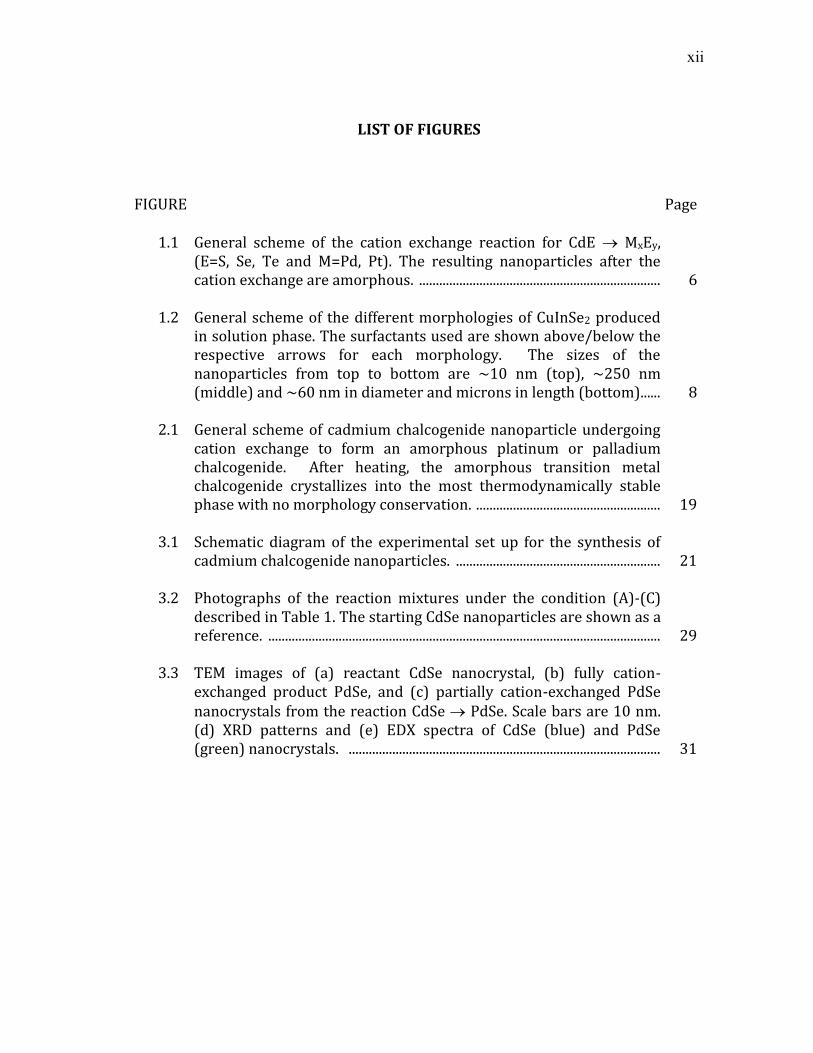
1.1 General scheme of the cation exchange reaction for CdE MxEy, (E=S, Se, Te and M=Pd, Pt). The resulting nanoparticles after the cation exchange are amorphous. ........................................................................ 6
1.2 General scheme of the different morphologies of CuInSe2 produced
in solution phase. The surfactants used are shown above/below the respective arrows for each morphology. The sizes of the nanoparticles from top to bottom are ~10 nm (top), ~250 nm (middle) and ~60 nm in diameter and microns in length (bottom)...... 8
2.1 General scheme of cadmium chalcogenide nanoparticle undergoing
cation exchange to form an amorphous platinum or palladium chalcogenide. After heating, the amorphous transition metal chalcogenide crystallizes into the most thermodynamically stable phase with no morphology conservation. ....................................................... 19
3.1 Schematic diagram of the experimental set up for the synthesis of
cadmium chalcogenide nanoparticles. ............................................................. 21 3.2 Photographs of the reaction mixtures under the condition (A)-(C)
described in Table 1. The starting CdSe nanoparticles are shown as a reference. ..................................................................................................................... 29
3.3 TEM images of (a) reactant CdSe nanocrystal, (b) fully cation-
exchanged product PdSe, and (c) partially cation-exchanged PdSe nanocrystals from the reaction CdSe PdSe. Scale bars are 10 nm. (d) XRD patterns and (e) EDX spectra of CdSe (blue) and PdSe (green) nanocrystals. ............................................................................................. 31

xiii
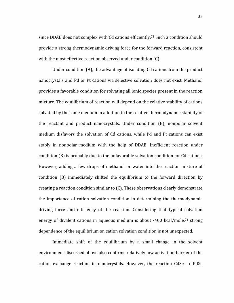
FIGURE Page 3.4 TEM images of (a-c) reactant, and (d-f) partially cation-exchanged
product nanocrystals from the reactions CdE PdE (E=S or Se). (a-c) are the images of CdS sphere, CdSe sphere and CdSe rod, respectively. (d-f) corresponds to the products from (a-c), respectively. Inserts in (d-f) are high resolution images of the product nanocrystals in each panel. Scale bars in (a-f) are 20 nm. (g-j) High resolution TEM images showing the progression of the cation exchange on zinc blend CdS nanocrystals with Pt cations. Scale bars in (g-j) are 2 nm. . ....................................................................................................... 35
3.5 TEM images of the reactant CdE (E=S,Se,TE) and fully exchanged
product nanocrystals. Reactant-product pair is indicated by an arrow connecting the two panels. (a-b) CdS-PdS, (c-d) CdSe-PdSe, (e-f) CdTe-PtTe, (g-h) CdSe-PdSe, (i-j) CdS-PtS, (k-l) CdSe-PtSe. Scale bars are 10nm. ................................................................................................ 38
3.6 XRD patterns of reactant (blue), product (green) and thermally
annealed product (red) nanocrystals from the cation exchange reaction CdE MxEy, (E= S, Se, Te and M=Pd, Pt). Reactant nanocrystals and exchanging metal ions are indicated in each panel. . 40
3.7 Experimental (blue) and simulated (green) XRD patterns of the fully
cation-exchanged (a) PdS and (b) PdSe nanocrystals. ............................... 41 3.8 XPS spectra of (blue) PtTe and (green) PtS. The values in
parentheses are taken from reported values in the literature. .............. 43 3.9 XPS spectrum of PdSe. For PdSe, literature values were not
available; however, the experimental values are in between binding energies of Pd2+ for PdS and PdTe. .................................................................... 44
3.10 TEM images of in-situ PdSe nanocrystals under different in-situ
heating conditions. (a) unheated, (b) 150C for 20 minutes, (c) 200C for 20 minutes, (d) 600C for 10 minutes. Inserts are the electron diffraction patterns for each sample. ............................................. 48
4.1 Crystal structure of chalcopyrite CuInSe2. Yellow, blue and red
represent selenium, indium and copper, respectively. .............................. 54

xiv
FIGURE Page 5.1 Reaction scheme illustrating the reaction of octyl magnesium
bromice with dibutyl phosphate to make dioctylphosphine oxide. ....... 67 5.2 TEM images of CuInSe2 nanocrystals prepared under the reaction
conditions of Table 1. (a) small nanospheres, (b) large nanospheres, (c) nanowires and (d) aggregates. ..................................................................... 69
5.3 XRD patterns of (a) small spheres, (b) large spheres, (c) nanowires
with magnified region around 35.5° and (d) aggregates. Red vertical lines indicate the peak positions for bulk phase of CuInSe2. ................... 70
5.4 (a) A single large CuInSe2 nanosphere with (b) corresponding high
resolution TEM image of large CuInSe2 nanospheres. ............................... 73 5.5 FT-IR spectra of (a) small spheres, (b) large spheres, (c) nanowires
and (d) large aggregates. The arrows indicate the peaks corresponding to the functional groups present in the surfactants. ..... 74
5.6 ESI-MS of CuInSe2 (a) nanowires and (b) large aggregates. .................... 77 5.7 (a) Skeletal structure of trioctylphosphine oxide (TOPO) and
dioctylphosphine oxide (DOPO). ........................................................................ 78 5.8 TEM images of CuInSe2 in different reaction conditions
corresponding to (a) TOPO only, (b) DOPO/TOPO=0.11, (c) DOPO/TOPO=0.67, (d) DOPO/ODE=0.67. ....................................................... 80
5.9 TEM image of (a) a nanowire, (b-d) SAED patterns of the nanowire
in the circled regions in (a). .................................................................................. 83 5.10 (a-b) Representative TEM images of nanowires. (c-d) HRTEM
images from the areas indicated in (b). Insets of (c-d) are theoretically modeled using material studio. ................................................ 84
5.11 (a) STEM image of a nanowire, (b) two locations of nanowires where
cross sectional views are obtained, (c-d) cross sectional view of nanowires obtained from reconstructed 3-dimensional tomogram at two locations shown in (b). ................................................................................. 86
5.12 Single nanowire with multiple cross sectional views. .............................. 87
xv
FIGURE Page 5.13 TEM images of the aliquots taken during the synthesis at the
reaction time of (a) 1 hour, (b) 1.5 hours and (c) 3 hours. ...................... 90 5.14 Electron diffraction patterns corresponding to Figure 5.15(a-c).
Diffraction spots corresponding to the (112) planes have been indexed and are shown by the red arrow. ...................................................... 90
5.15 (a) STEM image of a nanowire with three red lines corresponding to
the location of the EDX line scan. (b) The resulting line scans are shown and correspond to the labeled lines (1-3) on the STEM image. 91
5.16 (a) STEM image of a nanowire with three red lines corresponding to
the location of the EDX line scan. (b) The resulting line scans are shown and correspond to the labeled lines (1-3) on the STEM image. 92
5.17 (a) STEM image of two nanowires. Each nanowire has red lines that
correspond to the location of the EDX line scans. (b-c) The resulting line scans are shown and correspond to the labeled lines (1-4) on the STEM image. ........................................................................................................ 93

xvi
LIST OF TABLES
TABLE Page
3.1 Reaction conditions and solvent environments for cation exchange
reaction between cadmium chalcogenide nanocrystals (CdE) and metal chloride (MCln). ............................................................................................ 26
3.2 Structure, lattice parameter and fractional volume change of
reaction (V/V) for the reactant and possible product phases. ............. 45 5.1 Reaction conditions for CuInSe2 nanocrystals shown in the figure on
page 69. ......................................................................................................................... 65
1
CHAPTER I
INTRODUCTION
1.1 General background
Metal chalcogenide nanomaterials have interesting properties that differ
from their bulk counterparts. These properties depend not only on the material of
the nanoparticle but also on the size and shape of the particle as well. Spherical
semiconducting metal chalcogenide nanoparticles have tunable band gaps that are
dependent on the radius of the nanoparticle due to quantum confinement effects.1
Semiconducting nanorods have tunable band gaps as well, but the band gap
depends more strongly on the diameter of the rod than on the length. Emission
polarization is an example of a property in nanoparticles that is dependent on
shape, where the emission of spherical particles is depolarized, but the emission of
nanorods is linearly polarized.2 In addition, the chemical and physical properties of
nanoparticles can differ from their bulk counterparts as well. For example,
nanoparticles have a lower melting point than their bulk counterparts which can be
explained by the high surface to interior ratio of atoms in a nanoparticle.3
The synthetic methods of simple morphologies such as spheres, cubes and
rods/wires of binary phase metal chalcogenide nanoparticles have been well
studied.4-9 Binary metal chalcogenide nanoparticles have shown potential in
_________________ This dissertation follows the style of ACS Nano.

2
possible application such as emitting diodes, solar cells or lasers.1 Making more
complex nanostructures is the next step for nanoparticle synthesis. Specifically,
developing simple ways to make complex nanoparticles or modifying existing
nanoparticles (which already have a well developed synthetic method) may allow
nanoparticles to be more accessible for use in applications.
More complex nanostructures are desired for several reasons. The first
reason would be to have a single nanostructure with two different materials that
retain the individual properties. An example of this complex structure is having
both a semiconducting and a magnetic domain. This type of structure may be
useful in dual functional molecular imaging.10 The second reason to have a complex
nanostructure would be a single nanostructure in which the properties of one of
the materials strongly affect the properties of the other material. This type of
structure has been seen in type-II core/shell heterostructures. For example,
CdTe/CdSe core/shell structures emit in the near-IR region, which is not accessible
by either CdSe or CdTe nanoparticle by themselves.11 Knowing that complex
nanostructures can have advantages over simpler nanoparticles, the goal is to find
simple ways to make complex nanostructures.
Nanoparticles, whether simple or complex, can be made from either a top
down or bottoms up approach. Top down approaches take larger structures and
make them smaller, such as ball milling and laser ablation,12-14 but these methods
have several drawbacks that include trouble controlling shape or size distribution
and not being able to make very small particles. Bottoms up approaches use atoms

3
or molecules to make larger structures and are better suited to make uniform
nanostructures over the top down approaches. Bottoms up methods include liquid
or vapor phase epitaxy, template systems or colloidal methods.15 Colloidal
methods, or solution phase syntheses, have shown a high degree of control over the
size and shape of semiconducting, metal and metal oxide nanoparticles. This
control is achieved through regulation of thermodynamic parameters and growth
kinetics through the assistance of selected solvents, ligands, surfactants or
catalysts.16 Solution phase synthesis must precisely control multiple variables such
as temperature variation, choice of precursor, precursor concentration and solvent
and surfactant purity to obtain the desired morphology or size.
Solution phase growth of complex nanostructures has been studied in
numerous different systems with components such as semiconductors, metal
oxides and metals.17-28 Heterostructures can be made in numerous different ways
such as direct heterogeneous deposition, redox reactions, thermally induced phase
segregation, solid-state diffusion or ion exchange.16 The interface between the
different materials in the structure is just one of the considerations for solution
phase synthesis techniques. For materials with similar lattice constants, epitaxial
growth is expected and, as an example, core/shell structures can be made.29 When
the lattice mismatch is large, the resulting nanostructure can be harder to predict.
For example, noncentrosymmetric structures of γFe2O3 with MS (M = Zn, Cd, Hg)
were formed when large lattice mismatch is present.21 As the lattice mismatch
increased, structures went from multijunction particles to dimmers then to

4
completely separate particles with a few dimmers. In addition, a challenge of
solution phase synthesis is controlling the position of the different components in
complex nanostructures. For example, random nucleation of the second material or
the incorporation of mixed phases of materials are examples of why control is
limited for heterostructures.19
The previous materials discussed have been either binary or single element
nanoparticles (or domains in nanoparticles). Ternary or quaternary
nanostructures, with three or four elements respectively, are another example of
nanoparticles which are interesting. For example, I-III-VI2 materials such as
CuInSe2 have high optical absorption coefficients and are stable in the sun’s
radiation, which make them promising candidates for solar cell applications.30 In
addition, ternary (and quaternary) systems have much more tolerance in the
elemental composition of a given crystal phase, which can affect their material
properties such as ban gap. In CuInSe2 thin films, as the ratio of Cu/In increases the
band gap blue shifts.31 Another type of ternary material is an alloy (or solid
solution) such as PbSeyS1-y32 or CdSexTe1-x.32, 33 The ternary alloys have shown
promise because it allows for modification of properties based on composition, not
just size. In semiconducting nanoparticles of binary material, properties (e.g.
electronic or optical) are varied by changing the size of the nanoparticles; however,
in ternary alloys, it has been shown that by varying the ratio of Se to Te in CdSexTe1-
x alloy nanoparticles, the optical and electronic properties could be tuned (while
keeping size constant).33

5
Solution phase synthesis of ternary chalcogenide nanoparticles has unique
challenges as compared to binary chalcogenide nanoparticles. One of the main
challenges is the reaction of three or more different elemental precursors forming
the desired crystal structure.34 Balancing the decomposition temperatures or
ligand binding affinities of three or more elemental precursors are examples of why
the elemental composition of the nanoparticle can vary and be difficult to control.
The previous problem, coupled with shape and size control in the nanoscale region,
is why the synthetic methods of ternary or quaternary phases are not as developed
as binary systems.34
1.2 Simple routes for changing composition or morphology in nanomaterials
Understanding the problems that are encountered in the synthesis of
complex nanostructures (whether in composition or morphology) makes one
understand why finding simple ways to make complex nanostructures is of
importance. Conversion chemistry is an example of a simple technique to modify
composition or morphology in nanoparticles in which new and more complex
nanostructures can be made. Conversion chemistry uses a starting nanoparticle as
a template and transforms it into a chemically different species through the use of
ion exchange, diffusion, oxidation, galvanic replacement, etc.34
Diffusion and exchange of atoms in nanoparticles have been seen in many
systems and are a useful way to modify composition.34-38 The kinetics of a cation
exchange reaction (CdSe going to Ag2Se) was found to be much different in
6
nanomaterials than in bulk due to high collision efficiency values and low activation
energy.39 Cation exchange has been shown to be useful in the conversion of both
nano and mesoscale systems and are able to form more complex structures such as
heterostructres or periodic superlattices.35, 38, 40, 41
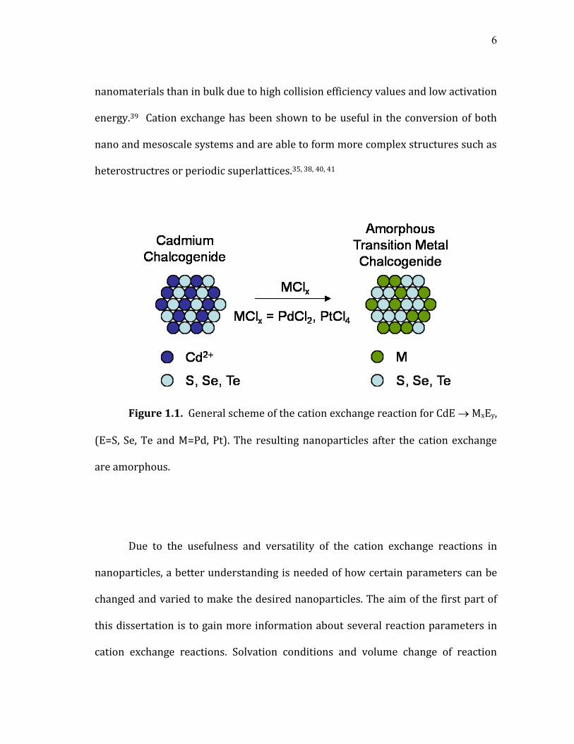
Figure 1.1. General scheme of the cation exchange reaction for CdE MxEy,
(E=S, Se, Te and M=Pd, Pt). The resulting nanoparticles after the cation exchange
are amorphous.
Due to the usefulness and versatility of the cation exchange reactions in
nanoparticles, a better understanding is needed of how certain parameters can be
changed and varied to make the desired nanoparticles. The aim of the first part of
this dissertation is to gain more information about several reaction parameters in
cation exchange reactions. Solvation conditions and volume change of reaction

7
were the chosen parameters because solvation studies may allow for the possible
tailoring and manipulation of the thermodynamics of the ion exchange reaction,
and the volume change of reaction allows insight into morphology conservation or
lack thereof. The goal of studying the cation exchange reaction is to establish a
framework which would allow the cation exchange reaction to be used in numerous
other systems.
Figure 1.1 illustrates a general scheme of the system of interest, starting
with nanoparticles of cadmium chalcogenide (S, Se or Te), which undergo a cation
exchange with either platinum or palladium cations. Both platinum and palladium
have a wide variety of stoichiometry with the chalcogenides that can be formed.
Platinum and palladium chalcogenides were studied because of their possible
applications in catalysis or in the semiconductor or electronics industry.42
The second project of this dissertation covers the development of a solution
phase synthesis of ternary chalcogenide nanoparticles. While the solution phase
synthetic methods of binary chalcogenide nanomaterials (such as CdSe) are well
understood, ternary chalcogenide are more difficult to make due to the complexity
of the phase diagram and reaction kinetics of the multi-component system. CuInSe2
was used as a model system because of its potential uses in photovoltaic or
thermoelectric devices.43-45 There have been numerous reports on the solution
phase synthesis of CuInSe2 nanoparticles which yield a variety of different
morphologies and sizes. Within these reports, though, is a lack of understanding of
how different synthetic variables affect the resulting morphology or size of the

8
nanoparticle. To this end, the purpose of the second project was to gain insight into
how surfactants specifically played a role in the morphology and size of ternary
chalcogenide nanoparticles. The goal would be to utilize this understanding which
would allow a simple way in which one could tune the morphology of ternary
semiconducting nanomaterials.
Figure 1.2. General scheme of the different morphologies of CuInSe2 produced in
solution phase. The surfactants used are shown above/below the respective arrows
for each morphology. The sizes of the nanoparticles from top to bottom are ~10
nm (top), ~250 nm (middle) and ~60 nm in diameter and microns in length
(bottom).

9
It was hypothesized that by changing the binding affinity of the surfactants
used, the morphology could be systematically varied. Oleylamine and
trioctylphosphine oxide (TOPO) were chosen as the strong and weak binding
surfactants, respectively. When a strongly binding surfactant was used, small
isotropic nanoparticles were formed, but when a weak binding surfactant was used,
larger anisotropic shapes were formed. When a combination of the two surfactants
was used, large isotropic nanoparticles were formed. Dioctylphosphine (DOPO), an
impurity found in TOPO, was found to be the key surfactant to make anisotropic
nanowires. Figure 1.2 shows the general scheme employed to make different
morphologies of CuInSe2.
To understand the role of the surfactant in the growth of anisotropic
particles, the nanowires were characterized at different times in the synthesis. It
was found that the nanowires had rough surfaces and grew by a continuous growth
mechanism. In addition the wires were polycrystalline and grew perpendicular to
(112) plane. Twinning occurred in the nanowires with a rotation around the
growth axis of ~60°.
1.3 Thesis overview
In the following chapters, the two experiments are explained in detail. The
background and principles of cation exchange in nanoparticles will be discussed in
Chapter II, and it will go into an in-depth discussion on cation exchange specifically
showing the usefulness of cation exchange as a simple way to modify composition

10
in nanoparticles. Chapter III follows explaining experimental details of the cation
exchange system showing the results along with the conclusions drawn from them.
Chapter IV will introduce surfactant direct morphology control and the issues for
making ternary chalcogenide nanomaterials in solution phase synthesis. Chapter V
includes the experimental data and the conclusions from the solution phase
synthesis of CuInSe2 nanoparticles with Chapter VI concluding the thesis.

11
CHAPTER II
THE USE OF CATION EXCHANGE IN NANOPARTICLES
2.1. Conversion chemistry in nanomaterials
Modification of nanoparticles which have a well developed synthetic method
is a simple way to make more complex nanostructures. “Nanocrystal conversion
chemistry” was a term coined by Schaak’s group that encompasses solution based
chemistry which takes a starting nanoparticle and chemically transforms it into
something else.34, 41 Numerous groups have studied methods for the transformation
of nanomaterials, which include galvanic replacement, oxidation, diffusion and ion
exchange.35, 46-49 Depending on the specific reaction conditions used, morphology
may or may not be conserved.50 The ultimate goal would be to understand fully all
types of transformations in the conversion chemistry of nanoparticles to give
scientists a “tool box” for which the production of complex nanostructures that
have the desired characteristics for potential applications becomes possible.34
Conversion chemistry uses nanoparticles with well established synthetic
procedures as reactive temples which can be partially or completely transformed.
Complete conversions, in regards to composition, can be useful to make
nanomaterials for which no synthetic methods are available. For example, Pt3Te3
nanoparticles were formed through a galvanic replacement between tellurium
nanowires and a platinum chloride salt. The authors state that this was the first
report of the synthesis Pt3Te3 nanomaterials.50 Metal nanoparticles could be turned
12
into metal phosphide nanoparticles with the use of phosphines, such as
trioctylphosphine. This is an example where a whole class of compounds which
could be accessed due to diffusion.46, 51-54
In respect to morphology, conversions, whether partial or complete, can
lead to a variety of complex nanostructures such as core/shell, tipped nanorods or
wires, or hollow nanoparticles. For example, hollow cobalt sulfide nanoparticles
were formed by taking cobalt nanoparticles and reacting them with sulfur in
dichlorobenzene. The void in the nanoparticle was formed due to differing
diffusion rate of the sulfur diffusing into the nanoparticle and the cobal diffusing
out (a Kirkendall-like mechanism).48 Core/shell structures could be made using
cation exchange to make CdSe/Ag2Se nanoparticles.55 Using galvanic reduction
reactions, silver tipped ZnO nanorod arrays could be formed.56
Conversion chemistry is not restricted to only the nanoscale regime. Xia and
coworkers make large mesoscale heterostructures of Se:Ag2Se by starting with Se
spheres of between 100 to 400 nm which were then reacted with Ag. The Se:Ag2Se
particles could then undergo a subsequent cation exchange to form Se:MSe (M=Zn,
Cd or Pb).41, 57 These previous examples show the versatility of nanoconversion
chemistry.
2.2 Ion exchange in nanoparticles
Chemical modification of nanocrystalline solids via diffusion or exchange of
atoms has been recently demonstrated to be a simple and versatile way to create a

13
variety of inorganic nanostructures.35, 41, 47, 49, 57-59 Cation exchange reaction in ionic
nanocrystals, in particular, has been shown to be very useful for transforming ionic
nanocrystals into other ionic nanocrystals, hetero-interfaced and periodic
superlattice nanostructures.35, 38, 57
Cation exchange had been extensively studied in thin films before it was
applied to nanoparticles.60, 61 Cation exchange in thin film showed that the
technique was advantageous because it was an economical and easy way to make
Ag2S thin films as compared to a direct chemical deposition method. In addition,
the thin films made by the cation exchange method had more desirable properties
(e.g. lower resistivity). After cation exchange, the crystal domains were ten times
smaller than the starting material (CdSe or CdS which had 2 to 3 micron domains),
and the exchange took anywhere from 15 minutes for CdS to Ag2S to 90 minutes for
CdSe to Ag2Se.60
Son and coworkers studied the same cation exchange reaction of CdSe with
Ag+ except in nanoparticles.35 It was found to be a fast and efficient way to modify
composition with the reaction taking less than 1 second.35 The crystal structure of
the reactant and product were similar and the reverse reaction of Ag2Se to CdSe
could be achieved by the addition of tributylphosphine (TBP). TBP forms an
intermediate complex with the Ag and, with the addition of gross excess of Cd2+,
forces the reverse reaction at slightly elevated temperatures. Only with the
addition of TBP will the reverse reaction proceed. In this example of cation
exchange, the ions were solvated in methanol, which was about 1% by volume of

14
the total solution. Due to the speed and reversibility of this reaction, the activation
barrier is thought to be rather small, and such fast kinetics and reversibility of the
reaction are considered mainly due to the lower activation barrier for the diffusion
of atoms in nanocrystalline solids. This example shows how the fundamental
kinetics of nanoparticles are drastically different than the bulk phase and even
differ from thin films as well.39
Other cation exchanges have been seen, such as ZnS with Cu+, Ag+, Sb3+ and
Bi3+.59 In this case of cation exchange, cations along with the starting reactants are
solvated in water. The solubility of the products formed was less than the
reactants, and the authors stated that this condition must be met for cation
exchange to take place. For reactions in which the solubility of the products is not
less than the reactants, some reaction condition needs to be changed to make the
reaction proceed, such as the addition of TBP.
Cation exchange was extended to mesoscale systems by Xia, et al. Se@Ag2Se
spheres were made, which can then be subsequently converted to Se@MSe (M = Zn,
Cd, Pb) with size and shape conversion.41, 57 The exchange reaction is performed in
only methanol. The TBP is known to bind with metal ions, but due to the stronger
interaction of TBP with Ag, the Zn, Cd, or Pb are left to exchange. All of these
exchanges were carried out at about 50°C. The authors comment that the use of
only methanol is needed for the reaction to take place and theorizes that the
methanol may act as a ligand along with the TBP.

15
For reactions that are not spontaneous, ligands, such as TBP, have been used
to complex with metal as seen in the reaction of Ag2Se to CdSe. The important idea
here is the ability to change the solubility of both cations, in the reactant and
product. In the previous examples of cation exchange, the solvent environment has
not been investigated to see what role it plays in the overall thermodynamic and
kinetics of the reactions. Understanding how solvent conditions along with ion
solubility affects ion exchange reactions will allow for better control and tailoring
of reaction conditions. Solvation studies will allow for possible tailoring of the
thermodynamics of the ion exchange reactions.
The previous discussion has been focused on solvation conditions, and the
use of complexing agents to allow the reverse cation exchange reaction to take
place. The crystal structure of the reactant and product nanoparticle also needs to
be discussed. An easy way to quantify the change of crystal structure is to calculate
the volume change of the unit cell from reactant to product, denoted by V/V. In
the previous cation exchanges discussed (of CdSe to Ag2Se and Ag2Se to ZnSe, CdSe
and PbSe), the V/V has been around 0.05 or 5%. This V/V is a relatively small
change, and the morphology or the nanoparticle is typically conserved. In order to
expand the use of cation exchange reactions to other systems, where V/V may be
much larger, more insight into how V/V affects the resulting morphology of the
nanoparticles is needed.
Anion exchange has proven more difficult in solution phase. This may be
due to the large size of the cation, but is more likely due to the stable anion

16
framework in ionic nanocrystals, specifically in transition metal chalcogenides. It
was found that the anionic framework was conserved during cation exchange with
the use of a CdSe/CdS nanorods.37 More complex starting heterostructures may
now be utilized in cation exchange reaction knowing that the anionic framework of
ionic nanocrystals is stable. That being said, anion exchange has been seen before
in a handful of systems, but typically the reaction conditions are harsher than those
of cation exchange reactions.59, 62, 63 For example, a ZnO columnar film was
transformed into ZnS by the use of H2S gas at around 500°C.59
In principle, the high efficiency of the cation exchange reaction in
nanocrystals can be extended more broadly to the exchange reactions with other
cations or possibly even anions.64 Ultimately, the efficiency of the cation exchange
reaction as a synthetic method will depend on the thermodynamic driving force
and the activation barrier. In order to utilize the cation exchange reaction as a
versatile synthetic method of nanocrystals, it will be important to understand and
perhaps control the factors affecting the kinetics and thermodynamics of the
reaction other than temperature and concentration. Since the net reaction involves
the exchange of two cations, solvation of cations is an important factor determining
the thermodynamics of the reaction. Cation solvation can be controlled to a certain
extent by varying the solvent environment, which will influence the overall
thermodynamics of the reaction. In the simplest case, one could vary the solvation
condition by changing the polarity of the solvent.

17
Consideration of the factors affecting the activation barrier is slightly more
complicated. The activation barrier for the diffusion and exchange of the cations
will depend on many factors such as the structure of anion sublattice, ionicity of
cation-anion interaction, structural difference between the reactant and product
phases, etc. Among these factors, the structural difference between reactant and
product phases is a more easily quantifiable factor and bears additional importance
concerning the morphology change of the nanocrystals after the reaction.
Morphology change of the nanocrystals, especially when the reaction accompanies
a large change in the volume or lattice parameters, can be an important issue when
the initial reactant nanocrystals are used as the structural template.35, 52, 59
In this work, the effect of solvent environment on the equilibrium and
efficiency of the cation exchange reaction was studied as well as the effect of
volume change of the reaction on the morphology change in the product
nanocrystals. The studied cation exchange reactions are CdE MxEy, (E=S, Se, Te
and M=Pd, Pt) occurring under ambient conditions, illustrated in Figure 2.1. The
fractional volume change (V/V) of reaction ranges from -0.25 to -0.46, based on
bulk lattice parameters.65-69 For all the reactions studied, the equilibrium of the
reaction was strongly dependent on the variation of the solvent environment,
which modified the thermodynamics of the reaction by changing the cation
solvation condition. In particular, a two-phase solvent environment, where the two
cations involved in the exchange reaction were separated in different phases,
strongly favored the forward reaction. This experimental evidence clearly indicates

18
the importance of the cation solvation by solvent medium in determining the
thermodynamic driving force and therefore the efficiency of the reaction. While all
the reactions were slower than the case of CdSe Ag2Se, the activation barrier was
still sufficiently low for the reaction to occur even at ambient temperature. These
results suggest the possibility of applying various selective cation complexing
reagents, more commonly used in organic reactions (e.g. crown ether), to enhance
the efficiency of the ion exchange reactions of nanocrystals. Relatively large V/V of
the reaction had varying degrees of effects on the morphology of the product
nanocrystals. Void formation and fragmentation, as well as the preservation of the
original morphology, were observed depending on the degree of lattice stress in the
product nanocrystals developed during the reaction. The platinum and palladium
chalcogenide nanoparticles made by cation exchange showed little crystallinity.
They were amorphous and with heating could be crystallized into the most
thermodynamic phases. Both in-situ and ex-situ experiments were performed.

19
Figure 2.1. General scheme of cadmium chalcogenide nanoparticles undergoing
cation exchange to form an amorphous platinum or palladium chalcogenide. After
heating, the amorphous transition metal chalcogenide crystallizes into the most
thermodynamically stable phase with no morphology conservation.

20
CHAPTER III
THE EFFECT OF ION SOLVATION AND VOLUME CHANGE OF REACTION ON THE
EQUILIBRIUM OF CATION EXCHANGE IN NANOPARTICLES*
3.1 Experimental section
3.1.1 Materials
The following chemicals were purchased from Aldrich and used without
further purification: Trioctylphosphine Oxide (TOPO 99%), palladium (II) chloride
(PdCl2, 99%), Platinum (IV) Chloride (PtCl4, 98%,) hexadecylamine, cadmium oxide,
sulfer, selenium, tellurium, tributyl phosphine, octadecene, oleic acide, octanonic
acid and didodecyldiethylammonium bromide. Tetradecylphosphonic acid and
hexylphosphonic acid was purchased from Polycarbon Industires, Inc.
3.1.2 Synthesis of cadmium chalcogenide nanoparticles
Spherical nanocrystals of CdS, CdSe and CdTe were synthesized following
the well-established solvothermal methods using CdO and elemental S, Se and Te
dissolved in coordinating solvents as precursors.7, 70, 71 Standard airless procedures
were used for all nanoparticle synthesis. Figure 3.1 illustrates the typical
____________ ✽ Reprinted in part with permission from J. Am. Chem. Soc. Wark, S. E.; Hsia, C. H.;
Son, D. H., Effects of ion solvation and volume change of reaction on the equilibrium and morphology in cation-exchange reaction of nanocrystals. J. Am. Chem. Soc. 2008, 130 (29), 9550-9555

21
experimental setup used to synthesis the cadmium chalcogenide nanoparticles.
Figure 3.1. Schematic diagram of the experimental set up for the synthesis of
cadmium chalcogenide nanoparticles.

22
CdSe nanoparticles were made using 0.012 mole (2.85 g) of hexadecylamine,
0.003 mole (1.15 g) of trioctylphosphine oxide, 0.004 mole (1.09 g) of
tetradecylphosphonic acid and 0.002 mole (0.250 g) of cadmium oxide which were
added into a three neck round bottom flask and heated under vacuum at 100-110
°C for I hour. The flask was then backfilled with nitrogen and heated to 300 °C until
the solution turned optically clear and 0.5 g TBP was injected. The temperature
was then lowered to 270 °C and an 0.8 gram solution of Se:TBP (10% by weight,
.001 mole of Se) was swiftly injected. The reaction was monitored by UV-Vis and
the reaction was stopped when the desired size was made. The reaction flask was
quickly cooled by blowing N2 around the bottom of the flask. When the solution
reached 60 °C, 10 g of octanonic acid was added to prevent the formation of a gel.
Methanol was then added until the solution was turbid. The solution was then
centrifuged and the supernatant was discarded. The supernatant should have a
slight yellow color from the octanonic acid, and the precipitate should be highly
colored. If a considerable amount of precipitate is observed, then you still have a
gel and it should be redisolved in toluene and octanonic acid. Once the supernatant
is discarded the precipitate should be dissolved in toluene and reprecipitated with
methanol.
CdS nanospheres were made using 0.5 mmole (0.064 g) CdO in 21.75 ml
ODE and 3.2 ml oleic acid which were added into a three neck round bottom flask
and heated under vacuum at 100-110 °C for I hour. This solution was heated under
N2 to 300 °C until the solution turned optically clear. The solution was cooled to

23
270 °C and 6.25 ml of S:ODE (0.625 mmole, 0.02 g of sulfur in 6.25 ml of ODE) was
swiftly injected. The growth temperature was held at 250 °C. The reaction was
monitored by UV-Vis and the reaction was stopped when the desired size was
made. The reaction flask was quickly cooled by blowing N2 around the bottom of
the flask. The reaction solution was cleaned with a dichloromethane:methanol (1:1)
extraction. The particles (which were in the dichloromethane layer were then
precipitated by adding acetone. The precipitate was redissolved in toluene. Two
more cleaning were done using methanol to precipitate and toluene to dissolve the
CdS nanoparticles.
CdTe nanospheres were made using 0.001 mole (0.13 g) of cadmium oxide
in 0.007 mole (1.95 g) TDPA and 0.017 mole (6.38 g) TOPO which were added into
a three neck round bottom flask and heated under vacuum at 100-110 °C for I hour.
The flask was then backfilled with nitrogen and heated to 300 °C until the solution
turned optically clear. The solution was then cooled to 270 °C and 2 g of Te:TOP
(10% by weight, 0.002 mole Te) was swiftly injected. The reaction was monitored
by UV-Vis and the reaction was stopped when the desired size was made. The
reaction flask was quickly cooled by blowing N2 around the bottom of the flask.
When the solution reached 60 °C, 10 g of toluene was added. Methanol was then
added until the solution was turbid. The solution was then centrifuged and the
supernatant was discarded. The precipitate was then redissolved in toluene and
cleaned twice more using methanol to precipitate and toluene to dissolve the CdTe
nanoparticles.
24
CdSe nanorods were synthesized following the procedure developed by
Peng et al.9 0.105 grams of cadmium oxide was mixed together with 0.39 grams of
tetradecylphosphonic acid, 0.08 grams hexylphosphonic acid and 1.425 grams of
trioctylphosphine oxide in a three neck round bottom flask. The flask was then
heated under vacuum at 100-110 °C for 30 minutes. The flask was then backfilled
with nitrogen and then heated to 300 °C until the solution turned optically clear.
Once the solution became clear, the heat was removed and the flask was then left at
room temperature for 24 hours under the nitrogen flow. After aging the solution,
the flask was then heated to 300 °C again until the mixture had dissolved. The heat
was lowered to 250 °C and 1.6 g of a 4% by weight solution of Se:TOP was swiftly
injected. The reaction was monitored by UV-Vis and the reaction was stopped when
the desired size was made. The reaction flask was quickly cooled by blowing N2
around the bottom of the flask. When the solution reached 60 °C, 10 g of toluene
was added. Methanol was then added to the solution until turbid and then the
solution is centrifuged. Both the nanorods and spheres were cleaned using
repeated precipitation by using methanol and redisolving the nanoparticles in
toluene. The nanoparticles were cleaned at least three times.
3.1.3 Cation exchange procedure
All the nanocrystals used in the cation exchange reactions were dispersed in
toluene. For the cation exchange reaction, PdCl2 and PtCl4 were used as the source
of cations. Three different reaction conditions that provided different cation

25
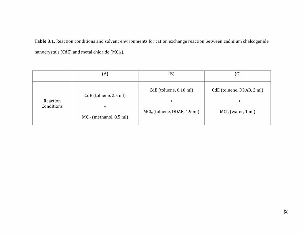
solvation environment were used as described in Table 3.1. The reactions occurred
in a single-phase solvent environment under condition (A) and (B), and in a two-
phase solvent environment under condition (C). Didodecyldiethylammonium
bromide (DDAB) used in condition (B) and (C) provided the metal salts solubility in
toluene, probably by forming a DDAB-metal chloride complex.72 In a simple
extraction experiment, approximately one equivalent of DDAB was needed to
extract one equivalent of metal ion from aqueous phase to organic phase. Typical
concentrations of the nanocrystals (CdE formula unit base) and metal salts (MCln)
in the final reaction mixture were approximately 0.1 mM and 5 mM respectively.
PdCl2 has limited solubility in methanol. To make the PdCl2 methanolic
solution, an excess of palladium salt (200 mg) was added to 3 ml of methanol. This
solution was sonicated for about 1 hour and then centrifuged. The supernatant
could then be used for the cation exchange procedure on that day. The solution
could not be used after a few days because the palladium could be reduced by the
methanol. A similar procedure was used for the PtCl4 methanolic solution with
PtCl4 being more soluble than the palladium salt in methanol. 350 mg of PtCl4 was
added to 3 ml of methanol and sonicated for 15 minutes. The solution was the
centrifuged and the supernatant could then be used for the cation exchange
procedure for that day. The platinum solution, just like the palladium solution,
could reduce the platinum to the metallic form.
26
Table 3.1. Reaction conditions and solvent environments for cation exchange reaction between cadmium chalcogenide
nanocrystals (CdE) and metal chloride (MCln).
(A) (B) (C)
Reaction Conditions
CdE (toluene, 2.5 ml)
+
MCln (methanol, 0.5 ml)
CdE (toluene, 0.10 ml)
+
MCln (toluene, DDAB, 1.9 ml)
CdE (toluene, DDAB, 2 ml)
+
MCln (water, 1 ml)

27
27
All the reactions were performed by mixing the nanocrystal solution with
the metal salt solution under ambient condition. The reaction time was varied from
a few minutes to several hours depending on the detailed reaction condition. After
the reaction, the product nanocrystals were precipitated by adding methanol and
centrifuging the reaction mixture. The recovered nanocrystals were rinsed with
methanol for further characterization of the structure and composition.
The platinum and palladium chalcogenide nanoparticles were amorphous
after exchange. Both in-situ and ex-situ heating experiments were preformed on
PdSe to observe how the nanoparticles would crystallize. In addition, ex-situ
experiments were performed on all the rest of the platinum and palladium
chalcogenides. The in-situ experiment was performed on a TEM grid which had a
Si3N4 window. This type of grid was used to withstand the heat and not degrade
under the high heat. A heating stage was used to control the temperature. For the
ex-situ heating experiment of the PdSe, 0.1 mmol of PdSe was added to 5 ml ODE
and heated to 200°C for 20 minutes. For the other platinum and palladium
chalcogenides, the nanoparticles were heated on a glass slide open to the air for 5
minutes. A solution of the nanoparticles was drop cast onto the glass slide and the
color of the thin film was observed to change from a brownish to black.
3.1.4 Characterization of nanoparticles
The lattice structures of the reactant and product nanocrystals were
examined by taking powder x-ray diffraction (XRD) patterns of the dried samples

28
28
on a Bruker-AXS GADDS diffractometer. Transmission electron micrographs (TEM)
of the nanocrystals were acquired using a JEOL 2010 transmission electron
microscope. For in-situ study of the structure of the thermally annealed
nanocrystals, TEM and electron diffraction patterns of the nanocrystal samples on
Si3N4 substrate were recorded before and after the heating. Elemental composition
of the nanocrystals was obtained from energy dispersive x-ray (EDX) analysis
employing Oxford Instruments INCA EDX system. Oxidation state of Pd and Pt
cations in the product phase was determined from x-ray photoelectron
spectroscopy (Kratos Axis Ultra).
3.2. Results and discussion
3.2.1 Effect of solvent on the equilibrium
In order to investigate the effect of cation solvation condition on the
equilibrium of the cation exchange reaction, three different reaction conditions
were used as described in Table 3.1. Under condition (A), metal cations were
solvated by a small amount of methanol homogeneously mixed with toluene. The
same condition was used for the reaction CdSe Ag2Se in earlier studies.35, 38
Under condition (B), both metal cations and reactant nanocrystals were in the
toluene phase. Under condition (C), Pd and Pt cations were initially in the aqueous
phase. During the reaction, DDAB transported Pd and Pt cations into toluene phase,
while the exchanged Cd cations were solvated in the aqueous phase.

29
29
Figure 3.2. Photographs of the reaction mixtures under the condition (A)-(C)
described in Table 1. The starting CdSe nanoparticles are shown as a reference.

30
30
When comparable total concentrations of the reactants were used, cation
exchange was the most efficient under condition (C), followed by condition (A) and
(B) for all the reactions investigated in this study. Figure 3.2 shows the
photographs of the reaction mixtures (CdSe nanocrystal and Pd salt solution) taken
several minutes after mixing the reactants under condition (A)-(C). The difference
in the extent of reaction can be seen from the colors of the reaction mixtures, since
the initial color of CdSe nanocrystal turns dark brown as the reaction proceeds. For
the reaction CdSe PdSe with 5nm CdSe nanocrystals, the reaction completed on
the order of 10 minutes under condition (C). Under condition (A), the product often
precipitated with only partial cation exchange during the same reaction time.
Condition (B) resulted in the least extent of reaction among the three reaction
conditions.

31
31
Figure 3.3. TEM images of (a) reactant CdSe nanocrystal, (b) fully cation-
exchanged product PdSe, and (c) partially cation-exchanged PdSe nanocrystals
from the reaction CdSe PdSe. Scale bars are 10 nm. (d) XRD patterns and (e)
EDX spectra of CdSe (blue) and PdSe (green) nanocrystals.
32
32
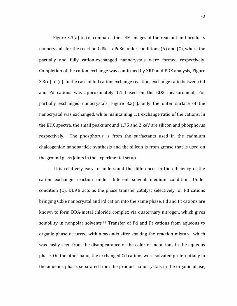
Figure 3.3(a) to (c) compares the TEM images of the reactant and products
nanocrystals for the reaction CdSe PdSe under conditions (A) and (C), where the
partially and fully cation-exchanged nanocrystals were formed respectively.
Completion of the cation exchange was confirmed by XRD and EDX analysis, Figure
3.3(d) to (e). In the case of full cation exchange reaction, exchange ratio between Cd
and Pd cations was approximately 1:1 based on the EDX measurement. For
partially exchanged nanocrystals, Figure 3.3(c), only the outer surface of the
nanocrystal was exchanged, while maintaining 1:1 exchange ratio of the cations. In
the EDX spectra, the small peaks around 1.75 and 2 keV are silicon and phosphorus
respectively. The phosphorus is from the surfactants used in the cadmium
chalcogenide nanoparticle synthesis and the silicon is from grease that is used on
the ground glass joints in the experimental setup.
It is relatively easy to understand the differences in the efficiency of the
cation exchange reaction under different solvent medium condition. Under
condition (C), DDAB acts as the phase transfer catalyst selectively for Pd cations
bringing CdSe nanocrystal and Pd cation into the same phase. Pd and Pt cations are
known to form DDA-metal chloride complex via quaternary nitrogen, which gives
solubility in nonpolar solvents.72 Transfer of Pd and Pt cations from aqueous to
organic phase occurred within seconds after shaking the reaction mixture, which
was easily seen from the disappearance of the color of metal ions in the aqueous
phase. On the other hand, the exchanged Cd cations were solvated preferentially in
the aqueous phase, separated from the product nanocrystals in the organic phase,
33
33
since DDAB does not complex with Cd cations efficiently.73 Such a condition should
provide a strong thermodynamic driving force for the forward reaction, consistent
with the most effective reaction observed under condition (C).
Under condition (A), the advantage of isolating Cd cations from the product
nanocrystals and Pd or Pt cations via selective solvation does not exist. Methanol
provides a favorable condition for solvating all ionic species present in the reaction
mixture. The equilibrium of reaction will depend on the relative stability of cations
solvated by the same medium in addition to the relative thermodynamic stability of
the reactant and product nanocrystals. Under condition (B), nonpolar solvent
medium disfavors the solvation of Cd cations, while Pd and Pt cations can exist
stably in nonpolar medium with the help of DDAB. Inefficient reaction under
condition (B) is probably due to the unfavorable solvation condition for Cd cations.
However, adding a few drops of methanol or water into the reaction mixture of
condition (B) immediately shifted the equilibrium to the forward direction by
creating a reaction condition similar to (C). These observations clearly demonstrate
the importance of cation solvation condition in determining the thermodynamic
driving force and efficiency of the reaction. Considering that typical solvation
energy of divalent cations in aqueous medium is about -400 kcal/mole,74 strong
dependence of the equilibrium on cation solvation condition is not unexpected.
Immediate shift of the equilibrium by a small change in the solvent
environment discussed above also confirms relatively low activation barrier of the
cation exchange reaction in nanocrystals. However, the reaction CdSe PdSe

34
34
exhibited much slower kinetics compared to CdSe Ag2Se studied earlier
suggesting higher activation barrier. In order to further examine the reversibility of
the reaction, an attempt to induce the reverse reaction PdSe CdSe was made. In
the case of Ag2Se, reverse reaction was completed within a minute when excess
amount of Cd cations was added to the solution of Ag2Se nanocrystals under
ambient condition. When PdSe nanocrystals were put under the same reaction
condition, the reverse reaction was not observed even with several hours of
reaction time, confirming the higher activation barrier than the case of Ag2Se.
Cation exchange reactions of CdS and CdTe with Pd and Pt cations exhibited the
same trend of solvent-dependent equilibrium as observed in reaction CdSe PdSe.
However, the reactions were generally faster in order of telluride to sulfide.
Completion of reaction CdTe PdTe occurred in several minutes, while CdS PdS
required ~1 hour of reaction time under condition (C).
35
35
Figure 3.4. TEM images of (a-c) reactant, and (d-f) partially cation-exchanged
product nanocrystals from the reactions CdE PdE (E=S or Se). (a-c) are the
images of CdS sphere, CdSe sphere and CdSe rod, respectively. (d-f) corresponds to
the products from (a-c), respectively. Inserts in (d-f) are high resolution images of
the product nanocrystals in each panel. Scale bars in (a-f) are 20 nm. (g-j) High
resolution TEM images showing the progression of the cation exchange on zinc
blend CdS nanocrystals with Pt cations. Scale bars in (g-j) are 2 nm.
36
36
3.2.2 Morphology of the partially cation-exchanged nanocrystals
In cation exchange reaction of the nanocrystals, the anisotropic morphology
of the nanocrystals was often preserved after the reaction.35, 52, 59 This indicates that
the frame of the anion sub lattice was maintained with only minor adjustments of
the ion positions, while cations were completely exchanged. In this case, the
reaction can be viewed as the diffusion of cations through the anion sub lattice that
has a limited flexibility. An interesting question that arises is where the exchange of
cations initiates on the nanocrystal and how the reaction propagates. To address
this question, intermediate structures with partial cation exchange were
investigated. Partially cation-exchanged products were obtained by precipitating
and washing the product nanocrystals before the completion of the reaction.
Figure 3.4 (a) to (f) compare the TEM images of the partially Pd-exchanged
nanocrystals produced from CdS and CdSe spheres and CdSe rods. In the case of
zinc blend CdS nanocrystals, Figure 3.4 (a) and (d), the regions of the reaction on
the nanocrystals coincide with the apexes of the tetragonal pyramid. Exchange with
Pt cations also resulted in the partially Pt-exchanged nanocrystals of the same
morphology. Figure 3.4 (g) to (j) shows the progression of the exchange reaction in
zinc blend CdS nanocrystals by Pt cations. Interestingly, the shape of the
nanocrystals becomes more faceted as the reaction continues. On the other hand,
partial cation exchange occurred homogenously on the outer surface of the sphere
in the case of wurtzite CdSe nanocrystals, Figure 3.4 (b) and (e), in contrast to CdS
nanocrystals. In wurtzite CdSe nanorods, Figure 3.4 (c) and (f), the reaction

37
37
occurred preferentially at both ends of the rod under condition (A), while the
preference was weakened under condition (C). These observations clearly
demonstrate that the initiation and progress of the cation exchange reaction
depends on the lattice structure and morphology of the reactant nanocrystals.
Preferential reaction at the tip of CdSe nanorods is reminiscent of the
formation of the semiconductor nanorods by solvothermal methods or reduction of
gold at the tip of semiconductor nanorods.9, 58 Anisotropic reaction to form
nanorods has been explained in terms of different accessibility of reactant
monomer to the different regions of the nanocrystals due to the selective
passivation of particular faces of the lattice by the surfactant molecules.9 An
analogous argument may be made to explain preferential exchange reaction at a
particular region of the nanocrystals observed in this study. In combination with
the steric factor described above, generally higher reactivity at the regions with
higher surface curvature and lower coordination number may also have played a
role in determining the preferred site for the initiation of the reaction.26 Formation
of the partially Pd and Pt-exchanged zinc blend CdS nanocrystals, where the
reaction occurred at four apexes of the tetragon, may be explained in this way.

38
38
Figure 3.5. TEM images of the reactant CdE (E=S,Se,Te) and fully exchanged product nanocrystals. Reactant-product
pair is indicated by an arrow connecting the two panels. (a-b) CdS-PdS, (c-d) CdSe-PdSe, (e-f) CdTe-PtTe, (g-h) CdSe-
PdSe, (i-j) CdS-PtS, (k-l) CdSe-PtSe. Scale bars are 10nm.

39
39
3.2.3 Structure and morphology of the fully cation-exchanged nanocrystals
Figure 3.5 compares the morphologies of the initial reactant and fully cation-
exchanged product nanocrystals from the reactions CdE MxEy, (E= S, Se, Te and
M=Pd, Pt). The reactions are categorized into three groups according to the nature
of the morphology change as will be discussed in detail below.
In order to characterize the lattice structure of the fully cation-exchanged
nanocrystals, XRD patterns of the reaction products were obtained. Figure 3.6
compares the XRD patterns of the reactant (blue) and product (green) phases.
However, the identification of the lattice structures of the product phase from XRD
pattern alone was not straightforward due to the very broad diffraction peaks and
the existence of multiple phases of Pd and Pt chalcogenides.
For Pd-exchanged nanocrystals, the exchange ratio between Pd and Cd
cations obtained from EDX measurements was approximately 1:1, indicating the
average oxidation state of +2 for Pd. Based on this result, the expected phases of the
product nanocrystals are PdS, PdSe and PdTe, which adopts tetragonal, tetragonal
and hexagonal structure respectively in bulk phase. Considering the very broad
diffraction peaks, it is likely that the product is in the disordered state of the
corresponding bulk phase. Similarity of the experimental XRD patterns of PdS and
PdSe nanocrystals to the theoretical XRD patterns calculated using their bulk lattice
parameters with the extra peak broadening introduced (Figure 3.7), further
supports the above conclusion.75, 76

40
40
Figure 3.6. XRD patterns of reactant (blue), product (green) and thermally
annealed product (red) nanocrystals from the cation exchange reaction CdE
MxEy, (E= S, Se, Te and M=Pd, Pt). Reactant nanocrystals and exchanging metal ions
are indicated in each panel.

41
41
Figure 3.7. Experimental (blue) and simulated (green) XRD patterns of the fully
cation-exchanged (a) PdS and (b) PdSe nanocrystals.

42
42
The theoretical peak broadening for the full width at half max calculations
was done with PowderCell using FWHM = f( U,V,W ). The crystal lattice constants
were not changed. For the broadening for PdS, U was 20.00, V was 200.00 and W
was 50.00. For the broadening for PdSe, U was 0.00, V was 100.00 and W was
50.00. While only the simulated broadened XRD of PdS and PdSe are showing in
Figure 3.7, the other systems (PdTe, PtS, PtSe and PtTe) were also analyzed. It was
found that all amorphous XRD data could be fit to simulated XRD using peak
broadening.
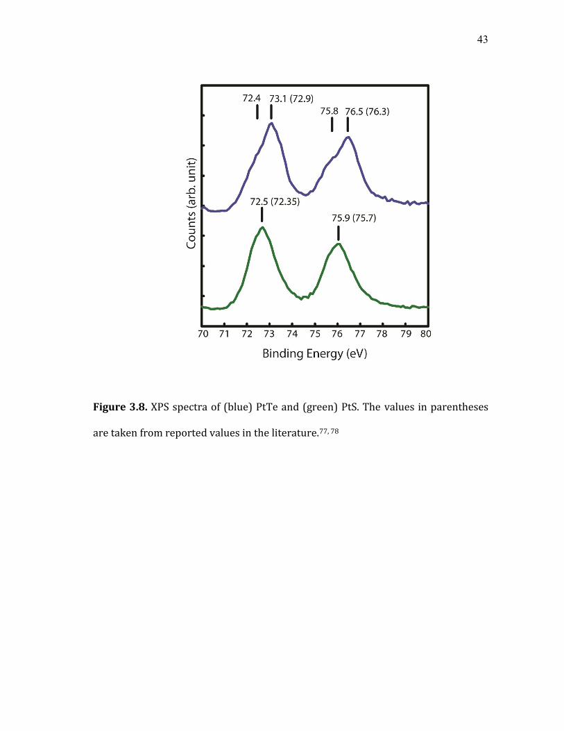
In the case of Pt-exchanged nanocrystals, the cation exchange ratio and the
oxidation state of Pt cations in the product phase measured from x-ray
photoelectron spectroscopy (XPS) was more complex, Figure 3.8. For sulfide, the
oxidation state of Pt cations was +2, consistent with the observed Pt:S ratio of 1:1 in
the product nanocrystals. In telluride, Pt cations exhibited mixed oxidation states of
+2 and +4, indicating more heterogeneous nature of the composition and
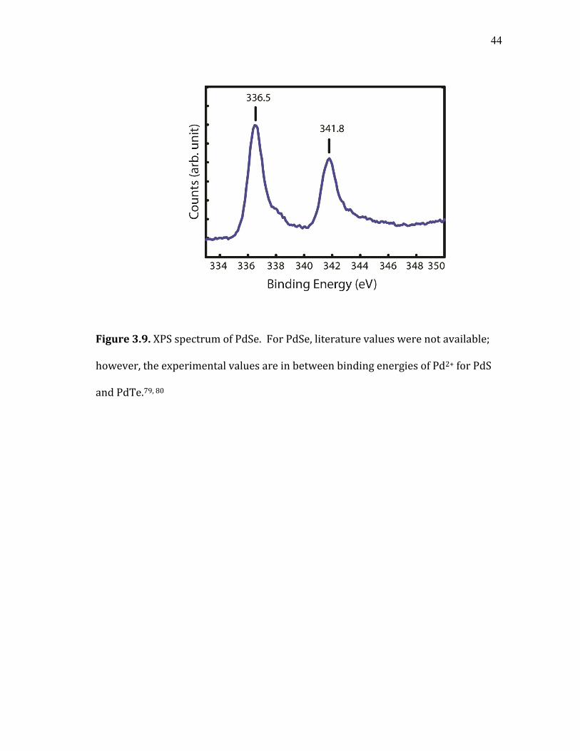
structure.77, 78 The XPS of PdSe nanoparticles is shown in Figure 3.9. Literature
value of PdSe could not be found, but the experimental values fall between that of
PdS and PdTe.79, 80
43
43
Figure 3.8. XPS spectra of (blue) PtTe and (green) PtS. The values in parentheses
are taken from reported values in the literature.77, 78
44
44
Figure 3.9. XPS spectrum of PdSe. For PdSe, literature values were not available;
however, the experimental values are in between binding energies of Pd2+ for PdS
and PdTe.79, 80

45
45
Table 3.2. Structure, lattice parameter and fractional volume change of reaction (V/V) for the reactant and possible product phases.
Material Structure Lattice parameter V/V
CdS Zinc Blende a=5.82 Reactant
PdS Tetragonal a=6.43, c=6.61 -0.30
PtS Tetragonal a=3.47, c=6.10 -0.25
PtS2 Rhombohedral a=3.54, c=5.04 -0.44
CdSe Wurtzite a=4.30, c=7.01 Reactant
PdSe Tetragonal a=6.73, c=6.91 -0.30
Pd17Se15 Cubic a=10.61 -0.29
PtSe2 Rhombohedral a=3.73, c=5.08 -0.45
Pt5Se4 Monoclinic a=6.58, b=4.61, c=11.12 -0.27
CdTe Wurtzite a=4.57, c=7.44 Reactant
PdTe Hexagonal a=4.13, c=5.66 -0.38
PtTe Monoclinic a=6.87, b=3.96, c=7.04 -0.33
Pt2Te3 Monoclinic a=6.93, b=4.00, c=17.12 -0.42
PtTe2 Hexagonal a=4.03, c=5.22 -0.46

46
46
If all the cation exchange reactions considered here produce stoichiometric
products with bulk equilibrium structures, V/V of reaction should range from -
0.25 to -0.46 as shown in Table 3.2. In comparison, V/V for CdSe Ag2Se studied
earlier is only 0.06 with very little (<1%) changes in the lattice parameters.35, 38 In
principle, a decrease in volume and/or a change of shape of the product
nanocrystals should be seen based on the theoretical values of V/V. However,
TEM images in Figure 3.5 shows varying degree of morphology changes depending
on the reaction and the size of the nanocrystals.
In Group 1, the product phase retains the original morphology. This is
observed in the reaction of small CdS and CdSe nanocrystals with Pd ions. V/V for
these reactions is approximately -0.3. In the case of the reaction CdSe PdSe,
Figure 3.5(c) to (d), contraction of the plane perpendicular to the c-axis by about
30% is the major change of the structure.69 However, contraction of the volume
corresponding to such structural change is not apparent in the TEM images. It is
possible that the product phase is kinetically frozen in a disordered and metastable
state, where the lattice stress in sustained without conforming to the equilibrium
lattice structure.
In Group 2, a void is formed inside the nanocrystals. This is observed in
PdSe, Figure 3.5 (g) to (h), and PtTe, Figure 3.5(e) to (f), especially for larger
nanocrystals. The void formation may be explained in terms of the release of the
stress in the lattice accumulated in the product phase during the reaction.81 The
stress that was sustainable during the early phase of the reaction may have reached
47
47
a critical point, which triggered the formation of the void from interior releasing
the stress in the lattice. Although the formation of the void is seemingly analogous
to the Kirkendall effect observed in earlier studies of CoxSy nanocrystals,49 the
origin of the void formation is different. In the case of the Kirkendall effect, void
formation is driven by the disparity of the diffusion coefficients of the two chemical
species propagating in the opposite direction. However, in the case of the cation
exchange reaction, it is the static anion sub lattice that determines the morphology
of the nanocrystals after the reaction.37
In Group 3, fragmentation of the nanocrystals to smaller pieces occurred.
This was observed in the reactions of CdS and CdSe nanocrystals with Pt cations,
Figure 3.5(i) to (l). Fragmentation may have resulted from continuous break-off of
the ion-exchanged parts from the main body of the reacting nanocrystal due to the
excessive lattice mismatch at the hetero interface. The resulting cation exchanged
product nanocrystals were very heterogeneous in size and much smaller than the
starting cadmium chalcogenide nanoparticles.

48
48
Figure 3.10. TEM images of in-situ PdSe nanocrystals under different in-situ heating conditions. (a) unheated, (b) 150
C for 20 minutes, (c) 200 C for 20 minutes, (d) 600 C for 10 minutes. (e) TEM image of ex-situ heated PdSe in ODE at
200 C for 20 minutes. Inserts are the electron diffraction patterns for each sample. Each scale bar is 10 nm.
49
3.2.4 Structure of the thermally annealed product nanocrystals
As discussed above, the product nanocrystals from cation exchange reaction
may have a significant lattice stress and disorder especially when the product
nanocrystals did not conform to the expected change of volume. In that case, the
product nanocrystals may transform to the thermodynamically more stable and
ordered phase via thermal annealing of the lattice. In order to see if the metastable
and disordered structure of the reaction product can relax to more equilibrated
structure, an in-situ TEM measurement of the thermally annealed product
nanocrystals was made. Thermal annealing was done by heating the nanocrystal
sample deposited on thin Si3N4 substrate in-situ on the temperature-controlled
sample holder of TEM. The sample was heated at several different temperatures.
The TEM image and electron diffraction patterns of the thermally annealed sample
were taken after cooling the sample stage to the ambient temperature.
Figure 3.10 shows the TEM images and electron diffraction patterns of the
PdSe nanocrystals before and after thermal annealing. After heating at 150 C for
20 minutes, Figure 3.10(b), the nanocrystals exhibit a noticeable reduction in size
compared to the unannealed PdSe nanocrystals, Figure 3.10(a). This is consistent
with our assumption that thermal annealing will transform to more equilibrated
structure of the product phase with V/V of -0.3. However, the structure of the
lattice still seems disordered based on the lack of well-defined diffraction patterns.
After further heating at 200 C for 20 minutes, the nanocrystals began to
form a crystalline phase with the increasing extent of agglomeration, Figure

50
3.10(c). The electron diffraction pattern in Figure 3.10(c) corresponds to Pd17Se15.
With continued heating at a higher temperature, the nanocrystals melted
completely. The diffraction pattern obtained after cooling down to the ambient
temperature clearly shows the diffraction rings corresponding to Pd17Se15, Figure
3.10(d). However, it is not entirely clear if the transformation to Pd17Se15 is purely
structural annealing or chemical disproportionation. In bulk phase, PdSe can
disproportionate into Pd17Se15 and PdSe2 above ~600 C.82 What is observed in
Figure 3.10(c) to (d) may be the combined result of structural annealing and
disproportionation. Ex-situ thermal annealing of PdSe nanocrystals in octadecene
at 200 C for 30 minutes also yielded Pd17Se15 nanocrystals. However, the annealed
nanocrystals were much larger than the original PdSe nanocrystals due to the
agglomeration. Other reaction products also exhibited agglomeration and
crystallization to more equilibrated structure upon ex-situ heating. XRD patterns of
the ex-situ heated samples are shown in Figure 3.6 (red curve in each panel).
Crystalline tetragonal PdS and PtS were formed from thermal annealing of the
disordered product nanocrystals. Heating of PdSe resulted in Pd17Se15 as described
above. Thermal annealing of the disordered PdTe resulted in mixed phases of PdTe
and PdTe2.

51
3.3 Conclusions
We have shown that equilibrium of the cation exchange reaction in
nanocrystals can be significantly changed by modifying the cation solvation
condition of the solvent medium. In particular, the equilibrium of the cation
exchange reaction could be shifted toward the formation of the product via
selective solvation of cations in a particular solvent phase. The effect of large
volume change of reaction on the morphology of the product phase has also been
studied. This is a particularly important issue when the reactant nanocrystal acts as
a morphological template. Depending on the stress developed in the lattice during
the reaction due to the difference of the lattice structure between the reactant and
product, the product nanocrystals underwent varying degree of morphological
changes, such as void formation and fragmentation. The knowledge on the effect of
ion solvation and V of reaction on the equilibrium and product morphology
obtained from this study provides a new strategy and useful guides to the
application of cation exchange reactions for the synthesis of a broader range of
inorganic nanocrystals.

52
CHAPTER IV
TERNARY I-III-VI2 CHALCOGENIDE NANOPARTICLES
4.1 Introduction
Ternary I-III-VI2 chalcopyrites and their solid solutions have received much
attention in the applications in photovoltaic and thermoelectric devices.43-45 For
example, CuInSe2 has a high absorption coefficient, suitable band gap (around 1 eV)
and stability in the sun’s radiation which lends well for its application in solar cell
devices.30 In addition, these materials are more environmentally friendly, seeing as
they do not contain toxic metals such as Cd (CdSe and CdTe have been studied and
proposed for solar cell applications as well).
CuInSe2 has two different structures, sphalerite and chalcopyrite. Chalcopyrite
is a crystal structure, similar to zinc blende, but with two different cations with one
anion. The anion is surrounded by two of each type of cation, and each cation is
surrounded by four anions. Due to the unequal sizes of the two cations, there is
tetrahedral distortion in contrast to the zinc blende structure. Figure 4.1 illustrates
the CuInSe2 chalcopyrite phase with yellow being Se, red being Cu and blue being
In. The sphalerite phase is similar to the chalcopyrite in that they have the same
anion sublattice, but the arrangement of the cations are different in that they are
randomly distributed. The chalcopyrite is the thermodynamically stable phase and
the phase most desired for CuInSe2 applications in devices. When synthesizing
nanomaterials of CuInSe2, it has been found that the order of addition of the Se

53
precursor can actually lead to the different phases of CuInSe2, which illustrates how
important it is to control the synthetic parameters to obtain the desired materials.83
For the remainder of this thesis, it will be implied that when talking about CuInSe2
it is the chalcopyrite phase unless otherwise indicated.
Temperature, elemental precursors, order of addition of the precursors and
reaction time are just a few of the experimental conditions that need to be
controlled to make the desired nanoparticle shape, size and composition. For
CuInSe2, balancing three different elemental precursors with different reactivity is
one of the many reasons why the synthetic methods of CuInSe2 (or any ternary
nanomaterials) are difficult. The properties of I-III-VI2 chalcopyrites depend on the
composition of the material; therefore, syntheses that make nanoparticles with
reliable composition is important.84, 85 In addition, the morphology of the
nanoparticles is important, and there has been success in making CuInSe2
nanomaterials of different morphology. For example, tetrahedron CuInSe2
nanoparticles were made using oleylamine as the solvent and surfactant with CuCl,
InCl3 and selenourea as the elemental sources.86 Larger structures of hexagonal
microplates were made in a combination of oleylamine and oleic acid with
elemental selenium and the acetylacetonate salts of copper and indium.87 A
nanoring morphology has even been made which used oleylamine,
trioctylphosphine, selenium, copper (I) chloride and indium trichloride.83
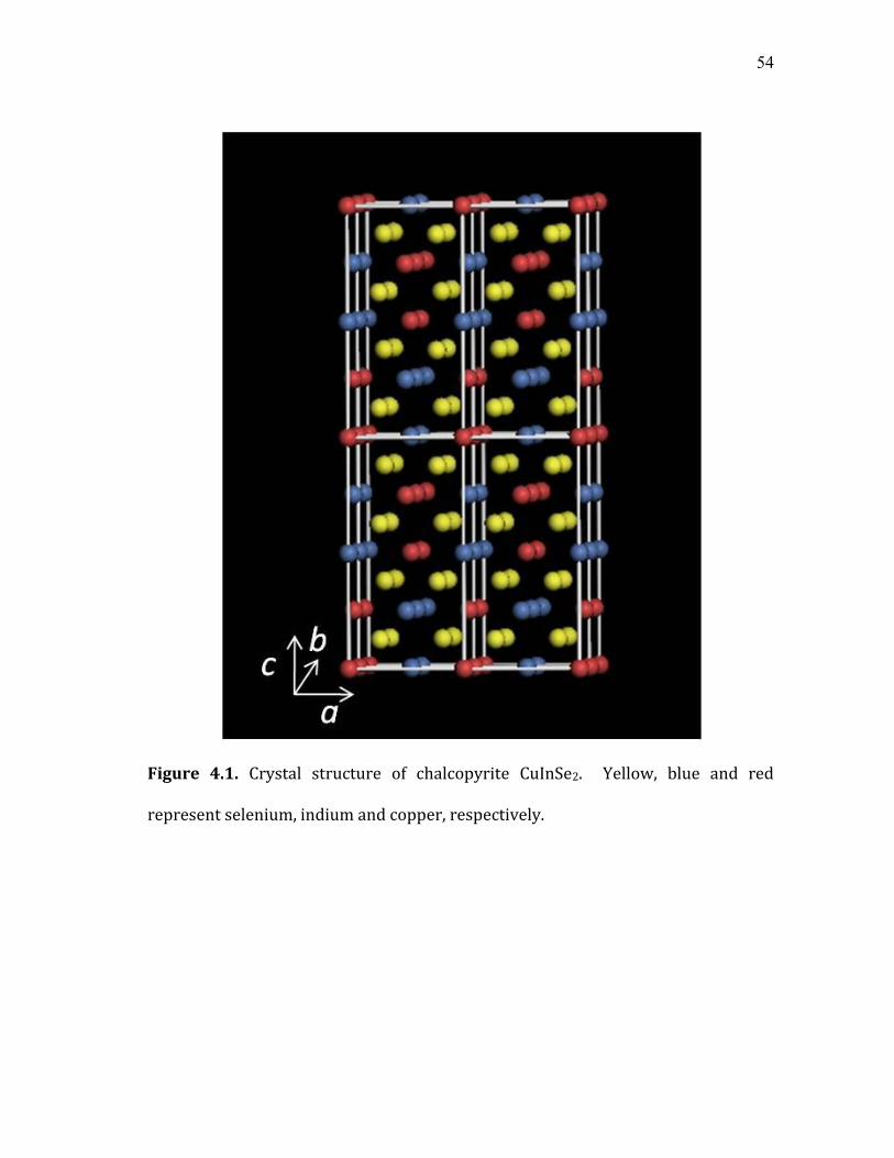
54
Figure 4.1. Crystal structure of chalcopyrite CuInSe2. Yellow, blue and red
represent selenium, indium and copper, respectively.

55
From the previous examples, it can be seen that synthetic methods with very
similar compounds yield very different morphologies. In general, the synthetic
methods that have been published focus more on the study of the material
properties of the synthesized substance, but no real progress has been made in
understanding the major synthetic variables of the Cu-In-Se system.
4.2 Methods to make anisotropic shaped nanoparticles
Recently, nanostructured chalcopyrites, particularly nanowires among other
structures, have attracted significant interest due to the advantages that 1-
dimensional nanostructures can offer in their device applications.83, 88, 89 Smooth,
single crystal, one-dimensional structures offer natural charge transport conduits
while rough one-dimensional structures may scatter phonons effectively and be
useful in thermoelectric materials. Due to the potential applications, understanding
how to make anisotropic ternary chalcogenide nanomaterials is of importance.
To understand the growth of anisotropic nanoparticles, an understanding of
the growth of isotropic nanoparticles is helpful. The growth of nanoparticles is
typically split into two stages, nucleation and growth. Nucleation occurs after the
reaction solution becomes supersatured with the monomer precursor. Growth
takes place after nucleation and incorporates the monomers left in the reaction
solution. If growth is left unchecked, then a corseting of the size distribution of the
nanoparticle will result. Researchers often try to separate these events, nucleation
and growth, to obtain better control over the resulting size and shape of the

56
nanoparticles. If the synthesis is kinetically controlled, then the rate at which the
different crystal faces grow dictates the shape of the nanocrystal. If the reaction is
thermodynamically controlled, then the resulting shape is due to a minimization of
the surface energy.
For the synthesis of anisotropic semiconducting nanoparticles, several
growth mechanisms have been proposed.4, 6, 90 The simplest model uses
thermodynamics to explain the shape control over crystals. The final shape of the
crystal will be determined by minimization the total free energy of the system. This
method has been useful in explaining some shape control in nanoparticles;
however, it cannot explain shape evolution in a single surfactant system.4
The selective-adsorption model explains how a mixed surfactant system
leads to anisotropic growth. Having two or more surfactants that selectively
adsorb to different crystal faces changes the surface free energy, allowing different
crystal faces to have unequal reactivity.91 The selective-adsorption model though
cannot explain anisotropic growth in single surfactant systems. For anisotropic
growth in a single surfactant system, typically multiple injections are used to
maintain monomer concentration. By maintaining a sufficiently high monomer
concentration, the relative differences in the different crystal faces’ growth rate can
be maintained, leading to anisotropic growth.91
Another type of mechanism that leads to anisotropic growth is the oriented
attachment model. Oriented attachment lowers the surface tension through
attachment of two smaller particles at a similar crystal face. This process can be

57
controlled through the controlled removal of surfactants on the surface, which was
shown in CdTe “pearl necklaces”.92 Oriented attachment illustrates the need to
understand how nanoparticles interact with each other, specifically the looking at
the intermolecular forces between them, such as dipole-dipole interactions.4
Solvents and surfactants can also act as molecular templates, which act as a
scaffold for nanomaterials to go on. This scaffold can be compared to a template,
and has been proposed in nanoparticle synthesis that uses ethylenediamine as
solvent and surfactant. While this model has been suggested, more experimental
proof is still needed.
Micelles have been used as a solution based method used to make a variety
of composition and shaped nanoparticles. The micelle method uses a surfactant
molecule that has both hydrophobic and hydrophilic interactions to spontaneously
form small surfactant aggregates of micelles that are typically spherical. If more
than one surfactant is used, other shapes can be made such as nanorods. The mixed
surfactant micelle system is similar to the one previously discussed of selective
adsorption, but due to the weaker binding of the micelle surfactants, it is probably
not the case.4
The final solution phase mechanism that will be discussed uses catalytic
nanoparticles to direct the anisotropic growth in nanomaterials. Solution-liquid-
solid (SLS), analogous to vapor-liquid-solid (VLS) growth mechanism, has been
shown to be very useful in making uniform nanowires.93 The catalytic nanoparticle
in solution directs anisotropic growth, but only at the interface between the
58
nanoparticle and the growing semiconductor is growth seen. The diameter of the
wires is dependent on the size of the catalytic nanoparticle.93 The nanoparticle
catalysts used must be molten under the reaction conditions to allow one of more
of the elemental precursors to be somewhat soluble to allow for supersaturation
and subsequent one-dimensional growth. The catalytic nanoparticles can either be
formed as a side product to the desired crystal phase or can be systematically
added into the reaction mixture. It was found that systematically adding known
concentrations and sizes of nanoparticles allowed for more controlled nanowire
synthesis.
While not a solution based method, template based methods such as AAO
tubes have shown success in making anisotropic nanoparticles, specifically
nanowires. The AAO tubes can vary in diameter from 10 to 2000 nm and the
composition can be varied by changing precursor mixtures. The nanowires are
electrochemically formed and, by changing the reaction conditions, can make wires
that range from a single material to more complex structures such as stripped
heterostructure with multiple materials.94, 95
4.3 Overview of CuInSe2 nanowire synthesis
Nanowires of various binary and ternary chalcogenide materials have been
prepared in a number of different ways.96-98 Among the methods that do not rely on
templates (e.g. anodic aluminum oxide tubes), the following two methods are the
most commonly used. One method is using metal nanoparticles as the catalyst

59
directing 1-dimensional anisotropic growth, in either vapor-liquid-solid (VLS) or
solid-liquid-solid (SLS) growth. The other option is solution phase synthesis
involving heating of precursors in a mixture of liquid solvent with surface-
passivating surfactants. Solution-phase synthesis of 1-dimensional structures that
do not use a metal nanocrystal catalyst or template rely on the anisotropic crystal
growth assisted by the anisotropic adsorption of surfactant molecules on different
facets during growth.9, 99 Both methods are relatively well established for the
growth of various binary semiconductor materials with some success applied to
ternary semiconductor materials.73, 100 However, it is generally more challenging to
synthesize ternary nanowires that are chemically and structurally homogeneous
due to the added complexity of the phase diagram and reaction kinetics of the
multi-component system.
In the case of CuInSe2, which is considered one of the most promising
materials in photovoltaic applications, preparation of nanowires from VLS and SLS
growth has been recently demonstrated by a number of groups.73, 100, 101 Methods
based on templating have also been used to form 1-dimensional structures.89, 102, 103
Solution-phase synthesis of CuInSe2 nanowires without a metal nanocrystal catalyst
or template has been less successful most likely due to the insufficient structural
anisotropy of the double zinc blende structure and weak anisotropic surfactant
passivation. So far, CuInSe2 nanocrystals of spherical and several other shapes, such
as tetrahedron, hexagonal plate or nanowiskers, have been made.86, 104-107

60
In this report, we describe a solution phase synthesis method that produces
multi-micron length nanowires of CuInSe2 without using a metal nanocrystal
catalyst. We show that the growth of CuInSe2 nanowires can be achieved by using
only a moderately binding surfactant, which may enhance the relatively weak
intrinsic anisotropy of the crystal growth. Since the shape of the nanocrystals in
solution phase synthesis depends on the surface energies of different facets that
decreases when passivated by the surfactant, the affinity of the surfactant
molecules is important in determining the nanocrystal shape.6 When the surfactant
is strongly adsorbing, the crystal facets with small intrinsic anisotropy may be
passivated without sufficient selectivity required for anisotropic growth. However,
surfactants with more moderate binding affinity will be less indiscriminate
passivating different facets potentially resulting in the stronger tendency for
anisotropic growth than with more strongly binding surfactants.
In this work, DOPO was identified as the key surfactant that leads to the
continuous growth of nanowires from anisotropic passivation of different facets.108
The synthesized nanowires often exhibited a saw-tooth pattern on the surface that
resembles a stack of truncated tetrahedra. The coherency of the lattice was
maintained better along the axial direction, while twinning around the growth axis
was observed. The highly modulated surface morphology in nanowires could be
potentially useful for nanoscale thermoelectric applications.109-112

61
CHAPTER V
SOLUTION-PHASE SYNTHESIS OF VARIOUS MORPHOLOGIES OF CUINSE2
NANOPARTICLES*
5.1 Experimental section
5.1.1 Materials
The following chemicals were purchased from Aldrich and used without
further purification: Trioctylphosphine Oxide (TOPO 99%), copper (I) chloride
(CuCl ≥99%), indium trichloride tetrahydrate (InCl3∙4H20, 97%), indium trichloride
(InCl3), selenium powder, oleylamine (technical grade, 70%), octylmagnesium
bromide in diethyl ether (2M), dibutylphosphite (96%), potassium carbonate
(K2CO3), octadecene (technical grade, 90%) and copper(II) acetylacetonate
(Cu(acac)2). The following chemicals were purchased from Strem and used without
purification: TOPO (99%), trioctylphosphine (TOP, 97 %)
5.1.2 Synthesis of CuInSe2 nanowires
CuInSe2 nanowires were made in solution phase using 10-3 mole (0.10 g) of
CuCl and 10-3 mole (0.29 g) of InCl3∙4H20 which were added into a mixture of 1.2 g
of TOPO, 0.8 g of dioctylphosphine oxide (DOPO) and 3 ml of TOP in a flask. The
____________ ✽ Reprinted in part with permission from J. Mater. Chem.. Wark, S. E.; Hsia, C. H.;
Luo, Z.; Son, D. H., Surfactant effect on the formation of CuInSe2 nanowires in solution phase synthesis. J. Mater. Chem.. 2011, DOI:10.1039/C1JM10401B
62
experimental set up is illustrated in figure 3.1. The flask was degassed under
vacuum at 100 °C for 1 hour. After refilling the flask with N2, the reaction mixture
was heated to 260°C. To initiate the reaction, 2 ml of 1M solution of Se in TOP
(TOP:Se) was injected into the flask. After 2-6 hours of reaction, the reaction
mixture was cooled down to room temperature and 20 ml of toluene was added.
The collected nanowires were rinsed in ethanol and precipitated repeatedly to
remove the remaining organic surfactants and other impurities.
Variations of this procedure using different solvent and surfactant molecules
were also used to investigate the effect of varying surfactant binding affinity on the
morphology of CuInSe2 nanocrystals. The amount of TOPO plus DOPO was held at a
constant 2.0 g. The ratio of the two was varied to study the resulting morphology of
the nanoparticles. In addition, ODE was substituted for TOPO, to understand the
role of TOPO in the synthesis. 1.2 ml of ODE was substituted for the 1.2 g of TOPO
in the nanowire synthesis.
As a side note, the reaction solution was found to be reactive with the
thermocouple used, prohibiting the formation of CuInSe2. To combat this problem,
a glass sleeve was used over the thermocouple. A slight amount of ODE was added
to the glass sleeve to assure that the thermocouple would read the correct
temperature of the solution in the round bottom flask. ODE was chosen because it
is a high boiling point solvent that is nonreactive.

63
5.1.3 Synthesis of CuInSe2 nanospheres
Small CuInSe2 nanoparticles were synthesized following a previously
reported method.104 2∙10-4 mole (0.053 g) of Cu(acac)2 (99.99 %, Aldrich) and 2∙10-
4 mole (0.044 g) of InCl3 (98 %, Aldrich) were added to 5ml of oleylamine (70 %,
Aldrich) in a flask and degassed at 100 °C for 1 hour then backfilled with N2 and
allowed to cool. Se dissolved oleylamine (OA:Se) was prepared by heating 0.04 g
(5∙10-4 mole) of Se powder in 8ml of oleylamine at 250 °C for 1 hour. The precursor
solution of Cu and In was then quickly injected into the hot OA:Se solution. After 30
minutes of reaction, the flask was cooled down to room temperature. Typically
spherical particles of >10 nm in diameter were formed in this way. To clean the
sample, 10 ml of toluene was added to the reaction solution and then methanol was
added until the solution became turbid. The solution was then centrifuged and the
supernatant was discarded. The precipitate was then redissolved in toluene. Two
more washings by methanol precipitation were then performed.
Larger spherical nanocrystals (50-250 nm in diameter) were synthesized
using the procedures similar to that of the nanowires. While the same Cu, In and Se
precursors were used, the reaction occurred in the mixture of TOPO (2 g), TOP (1
ml) and oleylamine (2 ml). The size of the nanocrystals was varied by varying the
reaction time. Growth could be seen in less than one minute and at 2 minutes the
CuInSe2 spheres were already 80 nm in diameter. If the small or large spherical
nanocrystals were not cleaned after synthesis, etching would occur due to
64
oleylamine. The synthetic conditions of the different types of CuInSe2 nanoparticles
are summarized in Table 5.1.
5.1.4 Structural characterization of the nanocrystals
The crystal structures of the synthesized nanocrystals were examined using
XRD and electron diffraction. Powder XRD patterns were obtained on a Bruker-AXS
GADDS diffractometer equipped with copper X-ray source and multi-wire
proportional counter as the detector. Electron diffraction patterns of the
nanocrystals were obtained on a JEOL 2010 TEM at an acceleration voltage of 200
kV. The same instrument, equipped with Oxford Instruments INCA EDX system, was
used to obtain both TEM images and elemental composition of the nanocrystal
samples. The 3-dimensional tomograms of the nanowires were obtained from a
series of zero-loss energy filtered TEM images acquired from FEI Tecnai G2 F20 FE-
TEM (200 kV) equipped with a tilting sample holder with ±60° angle range. The
TEM images taken at 1° tilt angle increment were processed with FEI Xplore3D
software employing the back-projection method to reconstruct the 3-dimensional
tomogram of the nanowires. The EDX analyses were done using FEI Tecnai F20 ST
TEM, with an EDAX EDX detector. The EDX drift-corrected line scan was performed
in the STEM mode using a beam spot size of 1 nm. Any specimen drifts during the
scanning were corrected by choosing a reference area nearby. Nickel TEM grids
were used instead of Cu grids for the EDX measurements.

65
Table 5.1. Reaction conditions for CuInSe2 nanocrystals shown in the figure on page 69.
(a) small spheres (b) large spheres (c) nanowires (d) aggregates
Solvent Oleylamine, 5 ml
TOPO, 2 g
Oleylamine, 2 ml
TOP, 1 ml
TOPO, 2 g
TOP, 3 ml
TOPO, 2 g
TOP, 3 ml
Cu, In source Cu(acac)2, 210-4 mole
InCl3, 210-4 mole
CuCl, 10-3 mole
InCl34H2O, 10-3 mole
CuCl, 10-3 mole
InCl34H2O, 10-3 mole
CuCl, 10-3 mole
InCl34H2O, 10-3 mole
Se source OA:Se, 510-4 mole TOP:Se, 210-3 mole TOP:Se, 210-3 mole TOP:Se, 210-3 mole
Total volume 13 ml 7 ml 7 ml 7 ml
Reaction
Time 30 minutes 30 minutes 4-6 hours 4-6 hours

66
66
5.1.5 Synthesis and characterization of dioctylphosphine oxide (DOPO)
DOPO, which is a key component for the synthesis of CuInSe2 nanowires,
was synthesized by employing a previously reported method.113 The reaction
scheme can be seen in Figure 5.1. 100 ml of 2 M octylmagnesium bromide in diethyl
ether was added to a 250 ml flask under oxygen-free condition. While keeping the
temperature of the flask in the range of 10-15 °C using an ice bath, 13.75 g of
dibutylphosphite was added drop wise at a rate of 0.12 ml/minute. After all the
dibutylphosphite was added, the temperature was raised to 35 °C to reflux for 30
minutes. Subsequently, the mixture was cooled down to 5-10 °C for the addition of
75 ml of 25 % aqueous H2SO4 solution over a 1 hour period. The ether layer
containing DOPO was separated from the mixture and rinsed with 25 ml of 18.2
MΩ∙cm deionized water three times. It was further rinsed with 25 ml of 15 %
aqueous solution of K2CO3 three times and 25 ml of deionized water three times.
Powder form of DOPO was obtained by evaporating ether at 65oC. The dried DOPO
was purified by recrystallization in n-hexane. The purity of the recrystallized DOPO
was >97%. The identity and purity of DOPO were determined by electrospray
ionization (ESI) mass spectrometry from the characteristic charge/mass ratio of
275 ([DOPO+H]+), 297 ([DOPO+Na]+) and 313 ([DOPO+K]+) in the mass spectrum.

67
67
Figure 5.1. Reaction scheme illustrating the reaction of octyl magnesium bromice
with dibutyl phosphate to make dioctylphosphine oxide.
5.2 Results and discussion
5.2.1 Effect of surfactant on the morphology of CuInSe2 nanocrystals
Selective surface passivation of surfactant molecules during the nanocrystal
growth is one of the key controls in solution phase synthesis of anisotropic
nanocrystals, such as nanowires. If the binding affinity of the surfactant on different
crystal facets is sufficiently different, unequal growth rates in different directions
can result in anisotropic morphologies. This strategy has been successful in
materials such as hexagonal wurtzite semiconductors, where the nanorods and
nanowires were grown along the c-axis via preferential passivation of facets
perpendicular to the growth axis.9, 99, 113 On the other hand, 1-dimensional growth
in zinc blende structures of these materials with cubic symmetry is more difficult
due to the higher symmetry of the crystal structure.114
In the case of chalcopyrite CuInSe2, the crystal structure is similar to zinc
blende but with two different types of cations (Cu+ and In3+) distributed in the
cation sites. Possibly due to the insufficient anisotropy of the crystal growth rate,

68
68
nanowires of CuInSe2 have been synthesized by using templates or metal
nanocrystal as the catalytic seed.73, 89, 94, 100-103 The reactions with well-passivating
surfactants, such as oleylamine and alkanethiols, usually give small spherical or
faceted nanocrystals.83, 87, 104 However, formation of anisotropic nanocrystals of
CuInSe2, such as hexagonal microplates, without the use of catalysts or templates
has also been reported indicating anisotropic crystal growth is possible although it
may be weak.83, 105-107 As mentioned in the Introduction section, when different
facets of the crystals do not have sufficient intrinsic anisotropy, surfactants with
weaker binding affinity may reveal the differences between facets more readily
than the surfactants with the stronger binding affinity. Based on this reasoning, we
performed a comparative study to test whether reducing the amount of a strongly
binding surfactant in the synthesis can enhance the anisotropic growth of CuInSe2
nanocrystals.

69
69
Figure 5.2. TEM images of CuInSe2 nanocrystals prepared under the reaction
conditions of Table 1. (a) small nanospheres, (b) large nanospheres, (c) nanowires
and (d) aggregates.
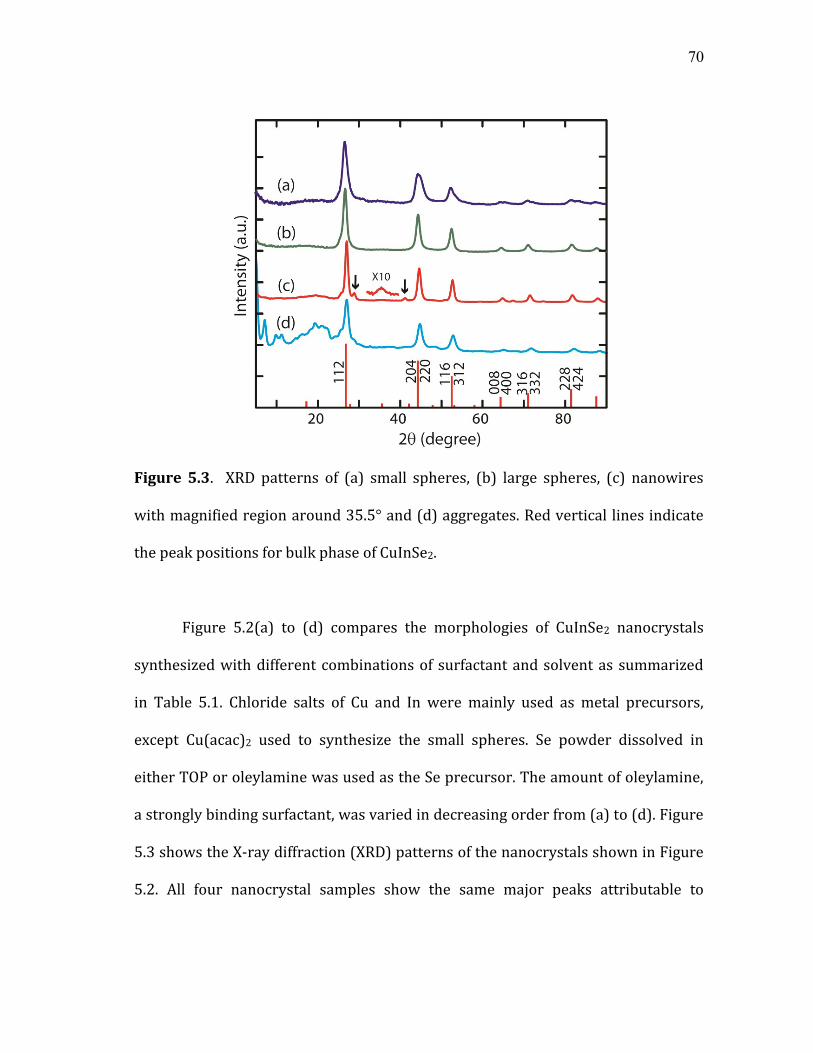
70
70
Figure 5.3. XRD patterns of (a) small spheres, (b) large spheres, (c) nanowires
with magnified region around 35.5° and (d) aggregates. Red vertical lines indicate
the peak positions for bulk phase of CuInSe2.
Figure 5.2(a) to (d) compares the morphologies of CuInSe2 nanocrystals
synthesized with different combinations of surfactant and solvent as summarized
in Table 5.1. Chloride salts of Cu and In were mainly used as metal precursors,
except Cu(acac)2 used to synthesize the small spheres. Se powder dissolved in
either TOP or oleylamine was used as the Se precursor. The amount of oleylamine,
a strongly binding surfactant, was varied in decreasing order from (a) to (d). Figure
5.3 shows the X-ray diffraction (XRD) patterns of the nanocrystals shown in Figure
5.2. All four nanocrystal samples show the same major peaks attributable to
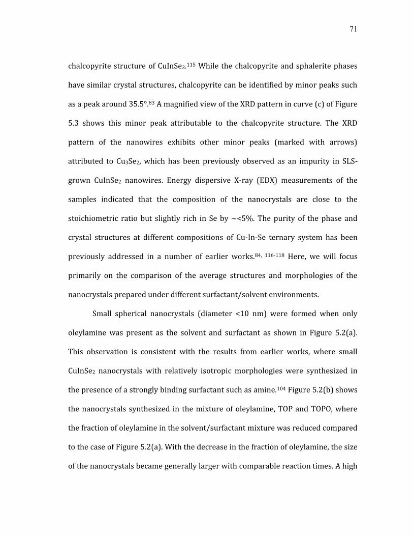
71
71
chalcopyrite structure of CuInSe2.115 While the chalcopyrite and sphalerite phases
have similar crystal structures, chalcopyrite can be identified by minor peaks such
as a peak around 35.5°.83 A magnified view of the XRD pattern in curve (c) of Figure
5.3 shows this minor peak attributable to the chalcopyrite structure. The XRD
pattern of the nanowires exhibits other minor peaks (marked with arrows)
attributed to Cu3Se2, which has been previously observed as an impurity in SLS-
grown CuInSe2 nanowires. Energy dispersive X-ray (EDX) measurements of the
samples indicated that the composition of the nanocrystals are close to the
stoichiometric ratio but slightly rich in Se by ~<5%. The purity of the phase and
crystal structures at different compositions of Cu-In-Se ternary system has been
previously addressed in a number of earlier works.84, 116-118 Here, we will focus
primarily on the comparison of the average structures and morphologies of the
nanocrystals prepared under different surfactant/solvent environments.
Small spherical nanocrystals (diameter <10 nm) were formed when only
oleylamine was present as the solvent and surfactant as shown in Figure 5.2(a).
This observation is consistent with the results from earlier works, where small
CuInSe2 nanocrystals with relatively isotropic morphologies were synthesized in
the presence of a strongly binding surfactant such as amine.104 Figure 5.2(b) shows
the nanocrystals synthesized in the mixture of oleylamine, TOP and TOPO, where
the fraction of oleylamine in the solvent/surfactant mixture was reduced compared
to the case of Figure 5.2(a). With the decrease in the fraction of oleylamine, the size
of the nanocrystals became generally larger with comparable reaction times. A high
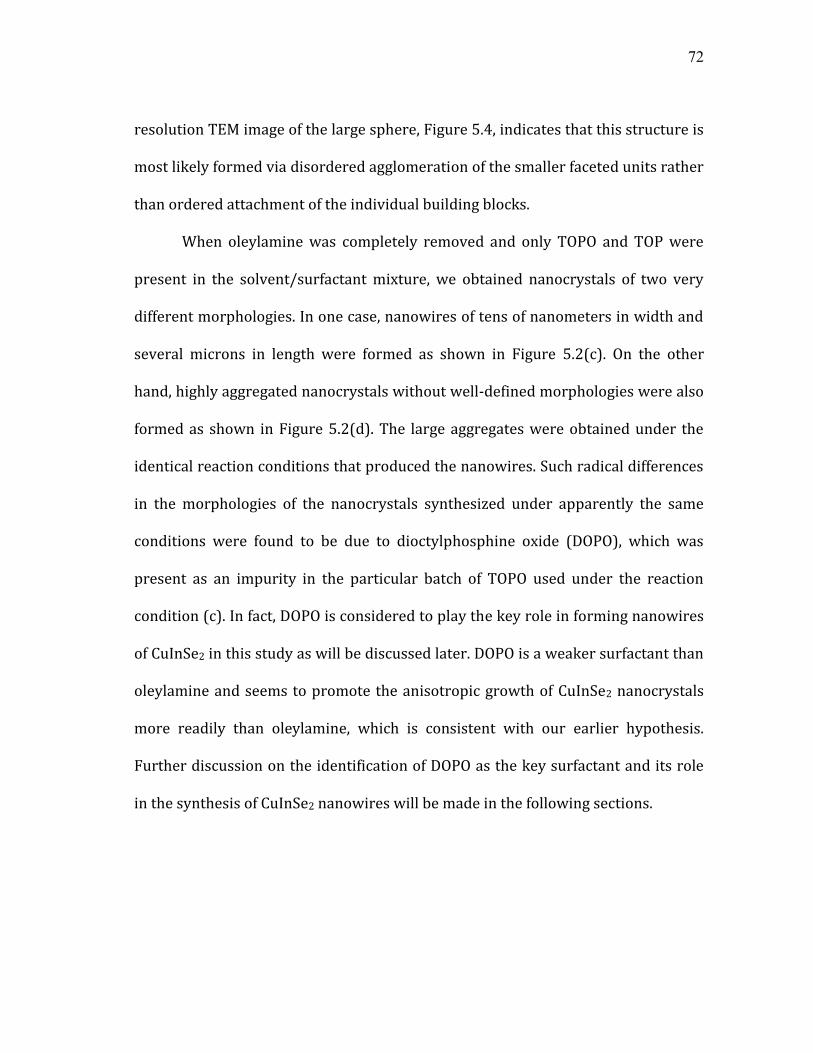
72
72
resolution TEM image of the large sphere, Figure 5.4, indicates that this structure is
most likely formed via disordered agglomeration of the smaller faceted units rather
than ordered attachment of the individual building blocks.
When oleylamine was completely removed and only TOPO and TOP were
present in the solvent/surfactant mixture, we obtained nanocrystals of two very
different morphologies. In one case, nanowires of tens of nanometers in width and
several microns in length were formed as shown in Figure 5.2(c). On the other
hand, highly aggregated nanocrystals without well-defined morphologies were also
formed as shown in Figure 5.2(d). The large aggregates were obtained under the
identical reaction conditions that produced the nanowires. Such radical differences
in the morphologies of the nanocrystals synthesized under apparently the same
conditions were found to be due to dioctylphosphine oxide (DOPO), which was
present as an impurity in the particular batch of TOPO used under the reaction
condition (c). In fact, DOPO is considered to play the key role in forming nanowires
of CuInSe2 in this study as will be discussed later. DOPO is a weaker surfactant than
oleylamine and seems to promote the anisotropic growth of CuInSe2 nanocrystals
more readily than oleylamine, which is consistent with our earlier hypothesis.
Further discussion on the identification of DOPO as the key surfactant and its role
in the synthesis of CuInSe2 nanowires will be made in the following sections.

73
73
Figure 5.4. (a) A single large CuInSe2 nanosphere with (b) corresponding high
resolution TEM image of large CuInSe2 nanospheres.
(a)
(b)

74
74
Figure 5.5. FT-IR spectra of (a) oleylamine (b) small spheres (c) large spheres, (d)
DOPO, (e) TOPO, (f) nanowires and (g) large aggregates. The arrows indicate the
peaks corresponding to the functional groups present in the surfactants.

75
75
5.2.2 Identification of surfactant molecules on the nanocrystal surface
In order to verify whether the different morphologies of CuInSe2
nanocrystals shown in Figure 5.2 correlate with the surfactant used, we attempted
to identify the surfactant molecules passivating the surface of the nanocrystals. For
this purpose, infrared (IR) absorption spectroscopy and mass spectrometry were
used. IR absorption spectra of thoroughly rinsed CuInSe2 nanocrystals with
different morphologies and pure surfactant are shown in Figure 5.5. An IR
spectrum, Figure 5.5 (b), obtained from the small spherical nanocrystals exhibits a
band attributed to the C=C stretching mode at 1652 cm-1 and N-H bending
(scissoring) mode at 1560 cm-1 indicating that oleylamine is passivating the
surface.119-121 IR spectra from the nanocrystals of Figure 5.2(c) and (d) (nanowires
and large aggregates) exhibit peaks attributed to P-O stretching modes near 1125
and 1045 cm-1 suggesting the presence of a phosphine oxide group coordinated to
both, Cu+ and In3+ ions.122 The IR spectrum from the large spherical nanocrystals,
Figure 5.2(b), has peaks that can be assigned to both amine and phosphine oxide
groups, consistent with the reaction condition containing both oleylamine and
TOPO.
The pure solvent IR spectra are shown on Figure 5.5 (a), (d) and (e). Pure
TOPO and DOPO only have one P-O stretching modes at 1142 and 1155 cm-1,
respectively, but due to the phosphine oxide potentially being bound to two
different cations, the splitting of the stretching mode could be explained by this.
The finger print region of the spectra is of interest as well. This region would give

76
76
some insight as to how the surfactant is bound to the nanoparticles. While there is
very little similarity in the finger print region from sample to sample or even
compared to the pure surfactant, theoretical modeling and calculations of the metal
surfactants bonding could be performed to gain a better understanding.
The IR data could not explain the difference in morphology of the samples
shown in Figure 5.2(c) and (d) as it would seem they are passivated by the same
molecule. So, to more clearly identify the surfactant molecules on the surface of the
samples shown in Figure 5.2(c) and (d), the mass spectra of the surfactant
molecules recovered from the surface of the thoroughly rinsed nanocrystal samples
were obtained. Initially, the nanocrystal samples rinsed with ethanol multiple times
were digested in 0.1% formic acid solution in the mixture of acetonitrile and water
(each 50% by volume). The supernatant recovered from the solution was analyzed
with ESI mass spectrometry. Figure 5.6(a) and (b) show the mass spectra of the
recovered supernatants from the nanowires and aggregates of CuInSe2
respectively. The mass spectra show both TOPO (m/z=387.4, [TOPO+H]+) and a
known impurity of TOPO, DOPO (m/z=313.3, [DOPO+K]+).113 The skeletal
structures of TOPO and DOPO are illustrated in Figure 5.7. DOPO has one less eight
carbon alkyl chain compared to TOPO.
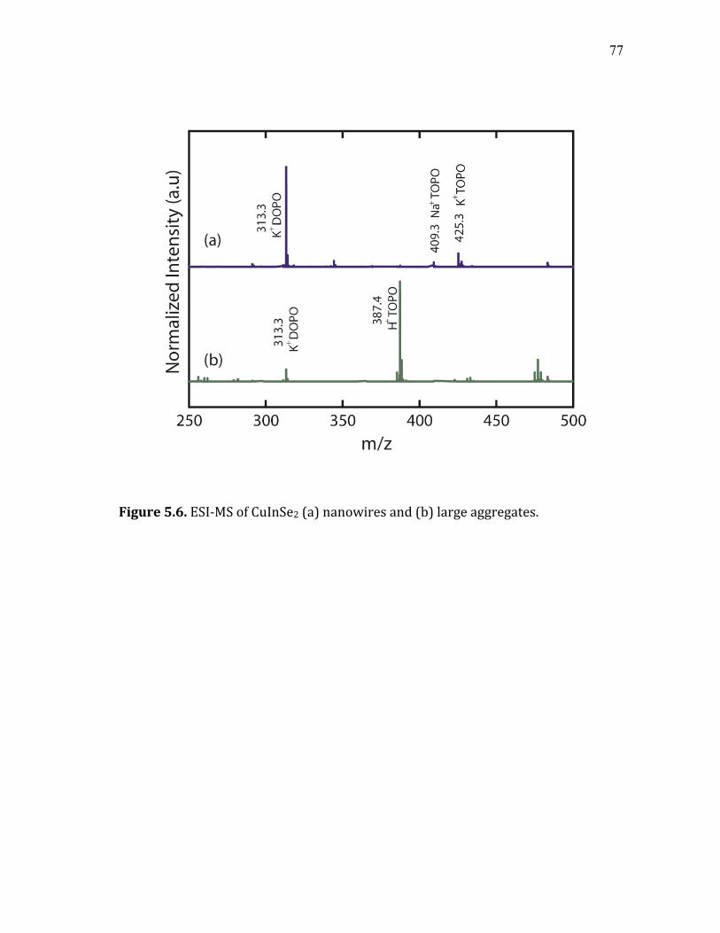
77
77
Figure 5.6. ESI-MS of CuInSe2 (a) nanowires and (b) large aggregates.

78
78
Figure 5.7. (a) Skeletal structure of trioctylphosphine oxide (TOPO) and
dioctylphosphine oxide (DOPO).

79
79
In order to further verify the role of DOPO in the formation of CuInSe2
nanowires, we compared the morphologies of the nanocrystals synthesized with
different proportions of DOPO to TOPO. For this purpose, we synthesized DOPO
following the procedure described in the experimental section. The purities of
DOPO and TOPO used for this comparative study were checked by ESI mass
spectrometry. DOPO was found to be >97% pure with small unidentifiable impurity
peaks using ESI-MS. 31P NMR spectra showed no sign of other phosphorous
impurities. 31P NMR of TOPO (Strem, >99%) showed no indication of contamination
by DOPO. The reactions were carried out in the surfactant and solvent mixtures of
four different compositions (mass ratio): (a) TOPO only, (b) DOPO/TOPO=0.11, (c)
DOPO/TOPO=0.67, (d) DOPO/octadecene=0.67. Composition (d), where TOPO was
replaced with non-coordinating hydrocarbon (octadecene, ODE), was tested to
further confirm the role of DOPO in forming the nanowires.

80
80
Figure 5.8. TEM images of CuInSe2 in different reaction conditions corresponding
to (a) TOPO only, (b) DOPO/TOPO=.11, (c) DOPO/TOPO=.67, (d) DOPO/ODE=.67.

81
81
Figure 5.8 compares the morphologies of the nanocrystals synthesized in
four different compositions of surfactant and solvent mixtures described above.
Only highly aggregated nanocrystals were obtained with >99% TOPO as the sole
solvent and surfactant. Nanowires were formed when DOPO was added to the
solvent mixture. The width of the nanowires decreased with increasing amount of
DOPO as can be seen in Figure 5.8(b) and (c). The average width of the nanowires
decreased with increasing amount of DOPO as can be seen in Figure 5.8(b) and (c)
from 56nm to 29nm respectively. In addition, the standard deviation of the width
of the wires also decreases by about 25%, with Figure 5.8(b) and (c) having a 42%
and 17% deviation respectively (roughly 50 nanowires were counted from each
batch). Nanowires could be formed even when TOPO was replaced with ODE that
does not possess any coordinating capability, while the nanowires were much
thicker than those obtained in the mixture of DOPO and TOPO. Mass spectra of the
surfactants recovered from all the nanowires showed DOPO as the main
component. These observations strongly indicate that DOPO is the key surfactant
responsible for the formation of nanowires of CuInSe2. The fact that TOPO is seen as
a minor component in the mass spectra of nanowires and that the replacement of
TOPO with ODE results in thicker nanowires suggests that TOPO also passivates the
surface of the nanocrystal although to a less degree than DOPO.
It is intriguing that DOPO is strongly preferred over TOPO on the surface of
CuInSe2 nanowires despite the fact that both surfactants have the same functional
group. The phosphine oxide group is considered to bind to cations on the surface of

82
82
various semiconductor nanocrystals.123, 124 In fact, one might expect that TOPO
would bind more strongly on the nanocrystal surface than DOPO since TOPO has
one more alkyl group that is more electron-donating than a hydrogen atom.
Therefore, the argument based on comparison of the coordinating capability of the
functional group alone may not explain the observation. On the other hand, DOPO
will experience less steric hindrance from the carbon chains than TOPO on the
surface of the nanocrystals. The smaller steric hindrance may be the reason why
DOPO is preferentially found on the surface of CuInSe2 nanowire. This observation
is also consistent with the earlier first-principle calculation study on the growth of
CdSe nanorods, where the less bulky surfactant preferred the anisotropic growth
more.125
5.2.3 Structure of CuInSe2 nanowires
In order to obtain more detailed structural information on CuInSe2
nanowires, selected-area electron diffraction (SAED) and high-resolution TEM
(HRTEM) measurements were made. Figure 5.9(a) to (d) show a TEM image of a
representative nanowire and SAED patterns obtained from the circled regions
along the nanowire. The wire growth direction is identified as normal to the (112)
planes (d112 = 0.33 nm). Since the selected areas contain multiple (112) nano-twins,
the diffraction spots split along this (112)* reciprocal direction. Figure 5.10(a) and
(b) show the TEM images of the nanowires obtained at higher resolution. HRTEM
images of two different regions of the nanowire indicated in Figure 5.10(b) are

83
83
displayed in Figure 5.10(c) and (d). These two regions exhibit a twinning
relationship around the growth axis with ~60° rotation about the common (112)
plane. A previous study has shown that twinning in chalcopyrite CuInSe2 occurs at
(112) planes.126 The indexed electron diffraction patterns and the lattice fringe
patterns in HRTEM images confirm that the nanowires grow perpendicular to the
(112) planes. The same growth direction was also observed in Wooten et al.’s work
employing SLS growth and Au/Bi nanocrystal catalyst.100
Figure 5.9. TEM image of (a) a nanowire, and (b-d) SAED patterns of the nanowire
in the circled regions in (a).

84
84
Figure 5.10. (a-b) Representative TEM images of nanowires. (c-d) HRTEM images
from the areas indicated in (b). Insets of (c-d) are theoretically modeled using
material studio.127
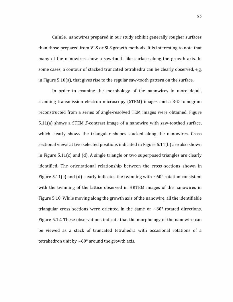
85
85
CuInSe2 nanowires prepared in our study exhibit generally rougher surfaces
than those prepared from VLS or SLS growth methods. It is interesting to note that
many of the nanowires show a saw-tooth like surface along the growth axis. In
some cases, a contour of stacked truncated tetrahedra can be clearly observed, e.g.
in Figure 5.10(a), that gives rise to the regular saw-tooth pattern on the surface.
In order to examine the morphology of the nanowires in more detail,
scanning transmission electron microscopy (STEM) images and a 3-D tomogram
reconstructed from a series of angle-resolved TEM images were obtained. Figure
5.11(a) shows a STEM Z-contrast image of a nanowire with saw-toothed surface,
which clearly shows the triangular shapes stacked along the nanowires. Cross
sectional views at two selected positions indicated in Figure 5.11(b) are also shown
in Figure 5.11(c) and (d). A single triangle or two superposed triangles are clearly
identified. The orientational relationship between the cross sections shown in
Figure 5.11(c) and (d) clearly indicates the twinning with ~60° rotation consistent
with the twinning of the lattice observed in HRTEM images of the nanowires in
Figure 5.10. While moving along the growth axis of the nanowire, all the identifiable
triangular cross sections were oriented in the same or ~60°-rotated directions,
Figure 5.12. These observations indicate that the morphology of the nanowire can
be viewed as a stack of truncated tetrahedra with occasional rotations of a
tetrahedron unit by ~60° around the growth axis.

86
86
Figure 5.11. (a) STEM image of a nanowire, (b) two locations of nanowires where
cross sectional views are obtained, (c-d) cross sectional view of nanowires obtained
from reconstructed 3-dimensional tomogram at two locations shown in (b).

87
87
Figure 5.12 Single nanowire with multiple cross sectional views.
88
88
5.2.4 Growth mechanism
In principle, CuInSe2 nanowires can form in a number of different ways
under our experimental condition. One possible mechanism is oriented attachment
of small tetrahedron units of CuInSe2. Formation of nanowires from smaller
building blocks via dipolar interaction between the building blocks has been
previously observed in a number of nanocrystals with cubic symmetry, such as
PbSe nanocubes.8 Since the lattice structure of CuInSe2 is double zinc-blende,
nanocrystals of tetrahedron morphology can be formed, which can be a potential
building block.86 The second possibility is SLS growth, analogues to Wooten et al.'s
work. While we did not add any metal nanocrystals as the catalytic seed, there is a
possibility that metal nanocrystals form in-situ and function as the catalytic seed. In
our reaction, it would most likely be the metallic indium, which is previously
known to catalyze nanowire growth of GaAs, Si, InAs and InP.128-130 Finally, CuInSe2
nanowires can form simply via anisotropic passivation of different facet during the
growth in the solution.
We ruled out the possibility of oriented attachment of tetrahedron building
blocks for the following reasons. Firstly, TEM images of the aliquots taken at
different times during the reaction did not show any signature of individual
nanocrystal building blocks, while longer reaction time generally resulted in the
growth of longer and thicker nanowires. Figure 5.13(a) to (c) show the morphology
of nanowires at the reaction time of from 1, 1.5 and 3 hours respectively, when the
reaction was performed with DOPO/TOPO mass ratio of 0.67. The electron

89
89
diffraction patterns that correspond to Figure 5.13 are shown in Figure 5.14. It can
be seen that the growth axis of parallel to (112) is maintained from the beginning of
the nanowire growth. Furthermore, formation of nanowires from the attachment of
tetrahedron units requires face-to-apex attachment for the whole length of the
nanowire, which is not a very probable event. A more likely scenario is the facet-
to-facet attachment of tetrahedron units, which would not lead to the linear
nanowire structure.
In order to check whether metallic indium is formed at any stage of the
reaction and function as the catalytic seed for SLS growth, aliquots taken at
different times during the reaction were analyzed with XRD. At any stages of
reaction, no signature of metallic indium could be found under our reaction
condition in XRD patterns. EDX line scan was also performed along the growth axis
at several regions including the both ends of the nanowire to identify potentially
indium-rich region that may indicate the presence of metallic indium seed, Figure
5.15 to Figure 5.17. Figure 5.15(a) and (b) show the regions of EDX line scan and
the corresponding elemental compositions. All three regions exhibit the nearly
identical composition showing no indication of metallic indium catalytic seed.
Figure 5.16 and 5.17 support this conclusion. According to the earlier studies on the
synthesis of indium nanocrystals, both high temperature (e.g. 360 C) and highly
reducing reagents (e.g. Na metal) are required to reduce InCl3 to metallic indium.
The absence of metallic indium in our reaction may be due to insufficiently
reducing condition to produce In0 from InCl3.131

90
90
Figure 5.13. TEM images of nanowire with at different growth times: (a) 1 hour,
(b) 1.5 hours and (c) 3 hours.
Figure 5.14. Electron diffraction patterns corresponding to Figure 5.15(a-c).
Diffraction spots corresponding to the (112) planes have been indexed and are
shown by the red arrow.

91
91
Figure 5.15. (a) STEM image of a nanowire with three red lines corresponding to the location of the EDX line scan. (b)
The resulting line scans are shown and correspond to the labeled lines (1-3) on the STEM image.

92
92
Figure 5.16. (a) STEM image of a nanowire with three red lines corresponding to the location of the EDX line scan. (b)
The resulting line scans are shown and correspond to the labeled lines (1-3) on the STEM image.

93
93
Figure 5.17. (a) STEM image of two nanowires. Each nanowire has red lines that
correspond to the location of the EDX line scans. (b-c) The resulting line scans are
shown and correspond to the labeled lines (1-4) on the STEM image.

94
94
Therefore, a more plausible route for the formation of CuInSe2 nanowires in
this study is continuous anisotropic growth assisted by the anisotropic surface
passivation by weak surfactant molecules. Figure 5.13, showing the time sequence
of the morphologies, also suggests that the nanowire is growing continuously both
in length and width. The growth of nanowires in the direction normal to (112)
plane may be due to the differences in the polarity of (112) plane forming the base
of tetrahedron and three {114} planes.86 The growth of nanowires in the direction
normal to (112) plane may be due to the differences in the polarity of (112) plane
forming the base of tetrahedron and three {114} planes. The (112) plane, composed
entirely of either all metal or selenium ions, may be better passivated by DOPO than
the other planes with both cations and anions resulting in anisotropic growth
perpendicular to (112) plane. Further computational study on the relative affinity
of DOPO and TOPO on different facets will shed an additional insight into the
mechanism of the growth of CuInSe2 nanowires.
5.3 Conclusions
Solution-phase synthesis of chalcopyrite CuInSe2 nanowires without using
metal nanocrystal catalyst has been demonstrated. The morphology of chalcopyrite
CuInSe2 nanoparticles can progress from an isotropic to a highly anisotropic shape
by varying the composition of strongly or weakly binding surfactants passivating
the surface of the nanocrystals. DOPO was found to be the key surfactant for the
growth of CuInSe2 nanowires. Detailed analysis of the nanowire structure indicates

95
95
that they grew normal to the (112) plane with twinning around the growth axis by
~60° rotation. The nanowires of CuInSe2 synthesized in this study exhibit an
interesting saw-tooth surface morphology resembling a stack of truncated
tetrahedra.

96
96
CHAPTER VI
CONCLUSIONS
6.1 General conclusions
6.1.1 Use of cation exchange to make transition metal chalcogenides
Transition metal chalcogenides, specifically platinum and palladium
chalcogenides, were made using a cation exchange reaction with cadmium
chalcogenide nanoparticles as the starting template. Cadmium chalcogenide
nanoparticles were chosen as the starting material due to the ease in controlling
shape and size of the nanoparticles. Solvation and volume change of reaction were
studied to set up a framework which would allow cation exchange to be extended
to more chemical compositions. It was found that by modifying the solvation
conditions of the cations, the equilibrium of the system could be changed. Three
different solvation conditions were studied, including a mixed solvent system, a
single solvent system with a complexing agent and a mixed solvent system with a
complexing agent. It was found that the mixed solvent system with the complexing
agent, condition (C), was the most efficient. Solvation condition (C) used DDAB to
solvate the reactant cations (either platinum or palladium) in toluene while the
product cations (cadmium) could then move to the aqueous phase.
The crystal structure of the product and reactant nanomaterials must also
be taken into account to predict the conservation or lack thereof for morphology.
Three different morphological changes were found to occur: morphology

97
97
conservation, void formation or fragmentation. The morphological changes were
found to result from the size and shape of the template nanoparticles as well as the
change in lattice structure.
6.1.2 Solution phase synthesis of CuInSe2 nanowires
Morphology of CuInSe2 nanoparticles could be tuned by varying the relative
amounts of surfactants with different binding affinities. Strongly binding
surfactants, such as oleylamine, lead to smaller, more isotropic shapes, whereas
weaker binding phosphine oxides gave much larger structures and allowed for
anisotropic growth. It was found that DOPO, a known impurity in TOPO, was
actually the key surfactant for anisotropic growth of CuInSe2 nanowires. The
nanowires which were made in a solution phase synthesis seem to grow without
the use of metal nanoparticle catalysts. It is believed that the difference in steric
bulk between TOPO and DOPO leads to the nanowire formation. Due to less steric
hindrance from DOPO, a higher packing density of the surfactant may occur on the
nanocrystal surface.
The nanowires were analyzed and found to have a rough surface. They grew
perpendicular to the (112) plane, were made up of truncated tetrahedrons and had
twinning around the growth axis by ~60°. The growth of the nanowires appeared
to be due to a continuous growth mechanism which showed no evidence of
catalytic growth.

98
98
6.2 Future directions
6.2.1 Extending cation exchange reactions
The experiments in Chapter 3 set up a framework to understand different
parameters in cation exchange reactions. The goal is to be able to use cation
exchange as an easy way to modify composition so as to obtain nanoparticles which
would otherwise be difficult or costly to make. In the previous experiments,
cadmium chalcogenide nanoparticles were used as the starting material and
template due to the well established synthetic procedures to make the
nanoparticles; however, in the future, it would be useful to only use other starting
nanoparticles, such as Zn or Cu chalcogenides, so as to eliminate the toxic cadmium
waste. For the platinum and palladium chalcogenide nanoparticles that were made,
the catalytic properties were studied using the Heck reaction in collaboration with
the Connell group. The nanoparticles did not act as a catalyst for the Heck reaction,
but the platinum and palladium chalcogenides may be useful for other catalytic
reactions such as hydrogenation reactions, which would be interesting to study.42
Further study of other complexing agents, for example crown ethers, which
will modify the solvation conditions, will be useful in order to make cation
exchange more accessible to other systems. Katari et al found that the excess
surfactants in the reaction solution can affect the kinetics of the reactions.123 This
knowledge may be useful to make more complicated compositions via cation
exchange such as ternary or even quaternary chalcogenides. Using two
simultaneous cation exchange reactions, for which the solvation conditions of the

99
99
cations has been selectively chosen, may allow for two cations to be exchanged for
one. Another possible way to approach making ternary nanomaterials would be to
using a partial cation exchange. As an example of a partial exchange, one could use
Cu2Se as the starting nanomaterial with a partial exchange of In cations. If the
resulting nanoparticles could then be annealing in solution, a ternary phase may be
accessible.
Another set of interesting experiments would be to study a ternary
nanoparticle undergoing cation exchange. One of two things could happen. The
first scenario would be that both cations in the ternary nanoparticle are exchanged
leading to a binary phase product. The other scenario would be that one of the two
cations in the ternary material will selectively exchange leading to another ternary
material. By making more complicated compositions of nanoparticles through the
use of cation exchange, the material properties of the ternary or quaternary
nanoparticles could then be studied in greater detail, allowing for possible
integration into devices due to the ease of synthesis.
6.2.2 Anisotropic growth in other ternary or quaternary chalcogenide
materials
The knowledge gained from the solution phase synthesis of different
morphologies of CuInSe2 may lead to other ternary or quaternary chalcogenide
synthetic routes. While the CuInSe2 nanowires will most likely not be efficient for
uses in solar cell devices because of their rough surface and polycrystalline

100
10
0
structure, they may be useful in other applications such as thermoelectric devices.
It would be interesting to study the material properties of the rough nanowires to
see how useful they could be. In addition, the understanding of how binding
affinity affects ternary structures may lead to better synthetic procedures for
quaternary chalcogenide materials. Quaternary chalcogenides are more difficult to
make in solution seeing as there are four elements in which to balance the
precursors’ reactivity to make one single crystal phase material. To date, there have
been numerous studies that look at CuInGaSe2 or similar materials in thin films for
the use in solar cell materials.132, 133 The next step would then be to find an easy
solution phase synthesis of high quality quaternary chalcogenide materials for use
in potential applications.
101
10
1
REFERENCES
1. Parak, W. J.; Manna, L.; Simmel, F. C.; Gerion, D.; Alivisatos, A. P., Quantum
dots. In Nanoparticles: From Theory to Application, Schmid, G., Ed. Wiley-
VCH: Weinheim, Germany, 2010; pp 3-47.
2. Scholes, G. D., Controlling the optical properties of inorganic nanoparticles.
Adv. Funct. Mater. 2008, 18 (8), 1157-1172.
3. Goldstein, A. N.; Echer, C. M.; Alivisatos, A. P., Melting in semiconductor
nanocrystals. Science 1992, 256 (5062), 1425-1427.
4. Kumar, S.; Nann, T., Shape control of II-VI semiconductor nanomateriats.
Small 2006, 2 (3), 316-329.
5. Manna, L.; Scher, E. C.; Alivisatos, A. P., Shape control of colloidal
semiconductor nanocrystals. J. Cluster Sci. 2002, 13 (4), 521-532.
6. Nair, P. S.; Fritz, K. P.; Scholes, G. D., Evolutionary shape control during
colloidal quantum-dot growth. Small 2007, 3 (3), 481-487.
7. Peng, Z. A.; Peng, X., Formation of high-quality CdTe, CdSe, and CdS
nanocrystals using CdO as precursor. J. Am. Chem. Soc. 2001, 123 (1), 183-
184.
8. Cho, K.-S.; Talapin, D. V.; Gaschler, W.; Murray, C. B., Designing PbSe
nanowires and nanorings through oriented attachment of nanoparticles. J.
Am. Chem. Soc. 2005, 127 (19), 7140-7147.

102
10
2
9. Peng, X. G.; Manna, L.; Yang, W. D.; Wickham, J.; Scher, E.; Kadavanich, A.;
Alivisatos, A. P., Shape control of CdSe nanocrystals. Nature 2000, 404
(6773), 59-61.
10. Gao, J. H.; Gu, H. W.; Xu, B., Multifunctional magnetic nanoparticles: Design,
synthesis, and biomedical applications. Acc. Chem. Res. 2009, 42 (8), 1097-
1107.
11. Kim, S.; Fisher, B.; Eisler, H. J.; Bawendi, M., Type-II quantum dots:
CdTe/CdSe(core/shell) and CdSe/ZinTe(core/shell) heterostructures. J. Am.
Chem. Soc. 2003, 125 (38), 11466-11467.
12. Munoz, J. E.; Cervantes, J.; Esparza, R.; Rosas, G., Iron nanoparticles produced
by high-energy ball milling. J. Nanopart. Res. 2007, 9 (5), 945-950.
13. Koch, C. C.; Whittenberger, J. D., Mechanical milling/alloying of
intermetallics. Intermetallics 1996, 4 (5), 339-355.
14. Milani, P.; DeHeer, W. A., Improved pulsed laser vaporization source for
production of intense beams of neutral and ionized clusters. Rev. Sci.
Instrum. 1990, 61 (7), 1835-1838.
15. de Dios, A. S.; Diaz-Garcia, M. E., Multifunctional nanoparticles: Analytical
prospects. Anal. Chim. Acta 2010, 666 (1-2), 1-22.
16. Carbone, L.; Cozzoli, P. D., Colloidal heterostructured nanocrystals: Synthesis
and growth mechanisms. Nano Today 2010, 5 (5), 449-493.
17. Fan, F. R.; Liu, D. Y.; Wu, Y. F.; Duan, S.; Xie, Z. X.; Jiang, Z. Y.; Tian, Z. Q.,
Epitaxial growth of heterogeneous metal nanocrystals: From gold nano-

103
10
3
octahedra to palladium and silver nanocubes. J. Am. Chem. Soc. 2008, 130
(22), 6949–6951.
18. Habas, S. E.; Lee, H.; Radmilovic, V.; Somorjai, G. A.; Yang, P., Shaping binary
metal nanocrystals through epitaxial seeded growth. Nat. Mater. 2007, 6 (9),
692-697.
19. Shi, W. L.; Zeng, H.; Sahoo, Y.; Ohulchanskyy, T. Y.; Ding, Y.; Wang, Z. L.;
Swihart, M.; Prasad, P. N., A general approach to binary and ternary hybrid
nanocrystals. Nano Lett. 2006, 6 (4), 875-881.
20. Yu, H.; Chen, M.; Rice, P. M.; Wang, S. X.; White, R. L.; Sun, S. H., Dumbbell-like
bifunctional Au-Fe3O4 nanoparticles. Nano Lett. 2005, 5 (2), 379-382.
21. Kwon, K. W.; Shim, M., gamma-Fe2O3/II-VI sulfide nanocrystal
heterojunctions. J. Am. Chem. Soc. 2005, 127 (29), 10269-10275.
22. Kwon, K. W.; Lee, B. H.; Shim, M., Structural evolution in metal
oxide/semiconductor colloidal nanocrystal heterostructures. Chem. Mater.
2006, 18 (26), 6357-6363.
23. Gu, H. W.; Zheng, R. K.; Zhang, X. X.; Xu, B., Facile one-pot synthesis of
bifunctional heterodimers of nanoparticles: A conjugate of quantum dot and
magnetic nanoparticles. J. Am. Chem. Soc. 2004, 126 (18), 5664-5665.
24. Pacholski, C.; Kornowski, A.; Weller, H., Site-specific photodeposition of
silver on ZnO nanorods. Angew. Chem. 2004, 43 (36), 4774-4777.

104
10
4
25. Carbone, L.; Kudera, S.; Giannini, C.; Ciccarella, G.; Cingolani, R.; Cozzoli, P. D.;
Manna, L., Selective reactions on the tips of colloidal semiconductor
nanorods. J. Mater. Chem. 2006, 16 (40), 3952-3956.
26. Kudera, S.; Carbone, L.; Casula, M. F.; Cingolani, R.; Falqui, A.; Snoeck, E.;
Parak, W. J.; Manna, L., Selective growth of PbSe on one or both tips of
colloidal semiconductor nanorods. Nano Lett. 2005, 5 (3), 445-449.
27. Talapin, D. V.; Koeppe, R.; Gotzinger, S.; Kornowski, A.; Lupton, J. M.; Rogach,
A. L.; Benson, O.; Feldmann, J.; Weller, H., Highly emissive colloidal CdSe/CdS
heterostructures of mixed dimensionality. Nano Lett. 2003, 3 (12), 1677-
1681.
28. Zhu, W.; Wang, W.; Shi, J., A reverse cation-exchange route to hollow PbSe
nanospheres evolving from Se/Ag2Se core/shell colloids. J. Phys. Chem. B
2006, 110 (20), 9785-9790.
29. Milliron, D. J.; Hughes, S. M.; Cui, Y.; Manna, L.; Li, J. B.; Wang, L. W.;
Alivisatos, A. P., Colloidal nanocrystal heterostructures with linear and
branched topology. Nature 2004, 430 (6996), 190-195.
30. Nadenau, V.; Braunger, D.; Hariskos, D.; Kaiser, M.; Koeble, C.; Oberacker, A.;
Ruckh, M.; Ruehle, U.; Schaeffler, R., Solar cells based on CuInSe2 and related
compounds: Material and device properties and processing. Prog.
Photovoltaics 1995, 3 (6), 363-382.

105
10
5
31. Bari, R. H.; Patil, L. A.; Patil, P. P., Structural, optical and electrical properties
of chemically deposited nonstoichiometric copper indium diselenide films.
Bull. Mater. Sci. 2006, 29 (5), 529-534.
32. Maikov, G. I.; Vaxenburg, R.; Sashchiuk, A.; Lifshitz, E., Composition-tunable
optical properties of colloidal IV-VI quantum dots, composed of core/shell
heterostructures with alloy components. ACS Nano 2010, 4 (11), 6547-6556.
33. Bailey, R. E.; Nie, S. M., Alloyed semiconductor quantum dots: Tuning the
optical properties without changing the particle size. J. Am. Chem. Soc. 2003,
125 (23), 7100-7106.
34. Vasquez, Y.; Henkes, A. E.; Bauer, J. C.; Schaak, R. E., Nanocrystal conversion
chemistry: A unified and materials-general strategy for the template-based
synthesis of nanocrystalline solids. J. Solid State Chem. 2008, 181 (7), 1509-
1523.
35. Son, D. H.; Hughes, S. M.; Yin, Y.; Alivisatos, A. P., Cation exchange reactions in
ionic nanocrystals. Science 2004, 306 (5698), 1009-1012.
36. Wark, S. E.; Hsia, C. H.; Son, D. H., Effects of ion solvation and volume change
of reaction on the equilibrium and morphology in cation-exchange reaction
of nanocrystals. J. Am. Chem. Soc. 2008, 130 (29), 9550-9555.
37. Jain, P. K.; Amirav, L.; Aloni, S.; Alivisatos, A. P., Nanoheterostructure cation
exchange: Anionic framework conservation. J. Am. Chem. Soc. 2010, 132
(29), 9997-9999.

106
10
6
38. Robinson, R. D.; Sadtler, B.; Demchenko, D. O.; Erdonmez, C. K.; Wang, L.-W.;
Alivisatos, A. P., Spontaneous superlattice formation in nanorods through
partial cation exchange. Science 2007, 317 (5836), 355-358.
39. Chan, E. M.; Marcus, M. A.; Fakra, S.; El Naggar, M.; Mathies, R. A.; Alivisatos,
A. P., Millisecond kinetics of nanocrystal cation exchange using microfluidic
x-ray absorption spectroscopy. J. Phys. Chem. A 2007, 111 (49), 12210-
12215.
40. Jeong, U.; Camargo, P. H. C.; Lee, Y. H.; Xia, Y., Chemical transformation: a
powerful route to metal chalcogenide nanowires. J. Mater. Chem. 2006, 16
(40), 3893-3897.
41. Jeong, U.; Kim, J.-U.; Xia, Y.; Li, Z.-Y., Monodispersed spherical colloids of
Se@CdSe: Synthesis and use as building blocks in fabricating photonic
crystals. Nano Lett. 2005, 5 (5), 937-942.
42. Dey, S.; Jain, V. K., Platinum group metal chalcogenides: their syntheses and
applications in catalysis and materials science. Platinum Met. Rev. 2004, 48
(1), 16-29.
43. Kuhn, B.; Kaefer, W.; Fess, K.; Friemelt, K.; Turner, C.; Wendl, M.; Bucher, E.,
Thermoelectric properties of CuIn1-xGaxTe2 single crystals. Phys. Status Solidi
A 1997, 162 (2), 661-671.
44. Lewerenz, H. J., Development of copper indium disulfide into a solar
material. Sol. Energy Mater. Sol. Cells 2004, 83 (4), 395-407.
107
10
7
45. Siebentritt, S., Wide gap chalcopyrites: Material properties and solar cells.
Thin Solid Films 2002, 403-404, 1-8.
46. Henkes, A. E.; Vasquez, Y.; Schaak, R. E., Converting metals into phosphides:
A general strategy for the synthesis of metal phosphide nanocrystals. J. Am.
Chem. Soc. 2007, 129 (7), 1896-1897.
47. Schaak, R. E.; Sra, A. K.; Leonard, B. M.; Cable, R. E.; Bauer, J. C.; Han, Y.-F.;
Means, J.; Teizer, W.; Vasquez, Y.; Funck, E. S., Metallurgy in a beaker:
Nanoparticle toolkit for the rapid low-temperature solution synthesis of
functional multimetallic solid-state materials. J. Am. Chem. Soc. 2005, 127
(10), 3506-3515.
48. Yin, Y.; Erdonmez, C. K.; Cabot, A.; Hughes, S.; Alivisatos, A. P., Colloidal
synthesis of hollow cobalt sulfide nanocrystals. Adv. Funct. Mater. 2006, 16
(11), 1389-1399.
49. Yin, Y.; Rioux, R. M.; Erdonmez, C. K.; Hughes, S.; Somorjai, G. A.; Alivisatos, A.
P., Formation of hollow nanocrystals through the nanoscale kirkendall effect.
Science 2004, 304 (5671), 711-714.
50. Samal, A. K.; Pradeep, T., Pt3Te4 nanoparticles from tellurium nanowires.
Langmuir 2010, 26 (24), 19136-19141.
51. Chen, J.-H.; Tai, M.-F.; Chi, K.-M., Catalytic synthesis, characterization, and
magnetic properties of iron phosphide nanowires. J. Mater. Chem. 2004, 14
(3), 296-298.

108
10
8
52. Henkes, A. E.; Schaak, R. E., Trioctylphosphine: A general phosphorus source
for the low-temperature conversion of metals into metal phosphides. Chem.
Mater. 2007, 19 (17), 4234-4242.
53. Khanna, P. K.; Jun, K.-W.; Hong, K. B.; Baeg, J.-O.; Mehrotra, G. K., Synthesis of
indium phosphide nanoparticles via catalytic cleavage of phosphorus carbon
bond in n-trioctylphosphine by indium. Mater. Chem. Phys. 2005, 92 (1), 54-
58.
54. Chiang, R.-K.; Chiang, R.-T., Formation of hollow Ni2P nanoparticles based on
the nanoscale kirkendall effect. Inorg. Chem. 2007, 46 (2), 369-371.
55. Han, M. Y.; Huang, W.; Chew, C. H.; Gan, L. M.; Zhang, X. J.; Ji, W., Large
nonlinear absorption in coated Ag2S/CdS nanoparticles by inverse
microemulsion. J. Phys. Chem. B 1998, 102 (11), 1884-1887.
56. Song, W.; Han, X. X.; Chen, L.; Yang, Y. M.; Tang, B.; Ji, W.; Ruan, W. D.; Xu, W.
Q.; Zhao, B.; Ozaki, Y., Site-specific deposition of Ag nanoparticles on ZnO
nanorod arrays via galvanic reduction and their SERS applications. J. Raman
Spectrosc. 2010, 41 (9), 907-913.
57. Camargo, P. H. C.; Lee, Y. H.; Jeong, U.; Zou, Z.; Xia, Y., Cation exchange: A
simple and versatile route to inorganic colloidal spheres with the same size
but different compositions and properties. Langmuir 2007, 23 (6), 2985-
2992.

109
10
9
58. Mokari, T.; Rothenberg, E.; Popov, I.; Costi, R.; Banin, U., Selective growth of
metal tips onto semiconductor quantum rods and tetrapods. Science 2004,
304 (5678), 1787-1790.
59. Dloczik, L.; Koenenkamp, R., Nanostructure transfer in semiconductors by
ion exchange. Nano Lett. 2003, 3 (5), 651-653.
60. Lokhande, C. D.; Gadave, K. M., A simple chemical method for conversion of
Cds into Ag2S and CdSe into Ag2Se. Mater. Chem. Phys. 1993, 36 (1-2), 119-
123.
61. Ristova, M.; Ristov, M., XPS profile analysis on Cds thin film modified with Ag
by an ion exchange. Appl. Surf. Sci. 2001, 181 (1-2), 68-77.
62. Park, J.; Zheng, H.; Jun, Y. W.; Alivisatos, A. P., Hetero-epitaxial anion
exchange yields single-crystalline hollow nanoparticles. J. Am. Chem. Soc.
2009, 131 (39), 13943–13945.
63. Cao, H. L.; Qian, X. F.; Wang, C.; Ma, X. D.; Yin, J.; Zhu, Z. K., High symmetric
18-facet polyhedron nanocrystals of Cu7S4 with a hollow nanocage. J. Am.
Chem. Soc. 2005, 127 (46), 16024-16025.
64. Koktysh, D. S.; McBride, J. R.; Dixit, S. K.; Feldman, L. C.; Rosenthal, S. J.,
PbS/PbSe structures with core-shell type morphology synthesized from PbS
nanocrystals. Nanotechnology 2007, 18 (49), 495607/1-495607/4.
65. Weinstein, M.; Wolff, G. A.; Das, B. N., Growth of wurtzite- CdTe and
sphalerite-type CdS single-crystal films. Appl. Phys. Lett. 1965, 6 (4), 73-75.
110
11
0
66. Traill, R. J.; Boyle, R. W., Hawleyite, isometric cadmium sulfide, a new
mineral. Am. Mineral. 1955, 40, 555-559.
67. Groenvold, F.; Haraldsen, H.; Kjekshus, A., On the sulfides, selenides, and
tellurides of platinum. Acta Chem. Scand. 1960, 14 (6), 1879-1893.
68. Geller, S., The crystal structure of Pd17Se15. Acta Cryst. 1962, 15, 713-721.
69. Villars, P., Ed., ASM Alloy Phase Diagrams Center;
http://www.asminternational.org/AsmEnterprise/APD, ASM International,
Materials Park, OH, 2006.
70. Reiss, P.; Bleuse, J.; Pron, A., Highly luminescent CdSe/ZnSe core/shell
nanocrystals of low size dispersion. Nano Lett. 2002, 2 (7), 781-784.
71. Yu, W. W.; Peng, X., Formation of high-quality CdS and other II-VI
semiconductor nanocrystals in noncoordinating solvents: Tunable reactivity
of monomers. Angew. Chem. 2002, 41 (13), 2368-2371.
72. Elliot, D. J.; Furlong, D. N.; Gengenbach, T. R.; Grieser, F.; Urquhart, R. S.;
Hoffman, C. L.; Rabolt, J. F., Reactions of complex-ions of platinum and
palladium in langmuir-blodgett-films of dimethyldioctadecylammonium
chlorometallates. Colloids Surf., A 1995, 103 (3), 207-219.
73. Peng, H.; Schoen, D. T.; Meister, S.; Zhang, X. F.; Cui, Y., Synthesis and phase
transformation of In2Se3 and CuInSe2 nanowires. J. Am. Chem. Soc. 2007, 129
(1), 34-35.

111
11
1
74. Marcus, Y., Thermodynamics of solvation of ions. Part 5.—Gibbs free energy
of hydration at 298.15 K. J. Chem. Soc., Faraday Trans. 1991, 87 (18), 2995-
2999.
75. Stanbery, B. J., Copper indium selenides and related materials for
photovoltaic devices. Crit. Rev. Solid State Mater. Sci. 2002, 27 (2), 73-117.
76. Kraus, W.; Nolze, G., POWDER CELL - a program for the representation and
manipulation of crystal structures and calculation of the resulting X-ray
powder patterns. J. Appl. cryst. 1996, 29, 301-302.
77. Dembowski, J.; Marosi, L.; Essig, M., Platinum disulfide by XPS. Surface
Science Spectra 1993, 2 (2), 133-137.
78. Dembowski, J.; Marosi, L.; Essig, M., Platinum sulfide by XPS. Surface Science
Spectra 1993, 2 (2), 104-108.
79. Elvy, S. B.; Williams, P. A.; Buckley, A. N., XPS evidence for the incongruent
surface oxidation of minerals in the Pd-Te-Bi system. Surf. Interface Anal.
1996, 24 (9), 641-646.
80. Volynsky, A. B.; Stakheev, A. Y.; Telegina, N. S.; Senin, V. G.; Kustov, L. M.;
Wennrich, R., Low-temperature transformations of sodium sulfate and
sodium selenite in the presence of pre-reduced palladium modifier in
graphite furnaces for electrothermal atomic absorption spectrometry.
Spectrochim. Acta, Part B 2001, 56B (8), 1387-1396.

112
11
2
81. Suh, Y. S.; Park, D. G.; Jang, S. A., Investigation of stress behaviors and
mechanism of void formation in sputtered TiSix films. Thin Solid Films 2004,
450 (2), 341-345.
82. Okamoto, H., The pd-se (palladium-selenium) system. J. Phase Equilib. Diffus.
1992, 13 (1), 69-72.
83. Guo, Q.; Kim, S. J.; Kar, M.; Shafarman, W. N.; Birkmire, R. W.; Stach, E. A.;
Agrawal, R.; Hillhouse, H. W., Development of CuInSe2 nanocrystal and
nanoring inks for low-cost solar cells. Nano Lett. 2008, 8 (9), 2982-2987.
84. Zhang, S. B.; Wei, S.-H.; Zunger, A.; Katayama-Yoshida, H., Defect physics of
the CuInSe2 chalcopyrite semiconductor. Phys. Rev. B Condens. Matter Mater.
Phys. 1998, 57 (16), 9642-9656.
85. Kemell, M.; Ritala, M.; Leskelae, M., Thin film deposition methods for CuInSe2
solar cells. Crit. Rev. Solid State Mater. Sci. 2005, 30 (1), 1-31.
86. Koo, B.; Patel, R. N.; Korgel, B. A., Synthesis of CuInSe2 nanocrystals with
trigonal pyramidal shape. J. Am. Chem. Soc. 2009, 131 (9), 3134-3135.
87. Zhong, H.; Li, Y.; Ye, M.; Zhu, Z.; Zhou, Y.; Yang, C.; Li, Y., A facile route to
synthesize chalcopyrite CuInSe2 nanocrystals in non-coordinating solvent.
Nanotechnology 2007, 18 (2), 025602/1-025602/6.
88. Panthani, M. G.; Akhavan, V.; Goodfellow, B.; Schmidtke, J. P.; Dunn, L.;
Dodabalapur, A.; Barbara, P. F.; Korgel, B. A., Synthesis of CuInS2, CuInSe2,
and Cu(InxGa1-x)Se2 (CIGS) nanocrystal "inks" for printable photovoltaics. J.
Am. Chem. Soc. 2008, 130 (49), 16770-16777.
113
11
3
89. Xu, J.; Luan, C.-Y.; Tang, Y.-B.; Chen, X.; Zapien, J. A.; Zhang, W.-J.; Kwong, H.-
L.; Meng, X.-M.; Lee, S.-T.; Lee, C.-S., Low-temperature synthesis of CuInSe2
nanotube array on conducting glass substrates for solar cell application. ACS
Nano 2010, 4 (10), 6064-6070.
90. Yin, Y.; Alivisatos, A. P., Colloidal nanocrystal synthesis and the organic-
inorganic interface. Nature 2005, 437 (7059), 664-670.
91. Manna, L.; Scher, E. C.; Alivisatos, A. P., Synthesis of soluble and processable
rod-, arrow-, teardrop-, and tetrapod-shaped CdSe nanocrystals. J. Am. Chem.
Soc. 2000, 122 (51), 12700-12706.
92. Tang, Z.; Kotov, N. A.; Giersig, M., Spontaneous organization of single CdTe
nanoparticles into luminescent nanowires. Science 2002, 297 (5579), 237-
240.
93. Wang, F. D.; Dong, A. G.; Sun, J. W.; Tang, R.; Yu, H.; Buhro, W. E., Solution-
liquid-solid growth of semiconductor nanowires. Inorg. Chem. 2006, 45 (19),
7511-7521.
94. Phok, S.; Rajaputra, S.; Singh, V., Fabrication of copper indium diselenide
nanowires. Mater. Res. Soc. Symp. Proc. 2008, 1031E (Nanostructured Solar
Cells), 1031-H13-28.
95. Liusman, C.; Li, S.; Chen, X.; Wei, W.; Zhang, H.; Schatz, G. C.; Boey, F.; Mirkin,
C. A., Free-standing bimetallic nanorings and nanoring arrays made by on-
wire lithography. ACS Nano 4 (12), 7676-7682.
114
11
4
96. Dresselhaus, M.; Lin, Y.-M.; Rabin, O.; Black, M.; Kong, J.; Dresselhaus, G.,
Nanowires. In Springer Handbook of Nanotechnology, 2nd ed., Bhushan, B.,
Ed. Springer Berlin Heidelberg: 2007; pp 113-160.
97. Fan, H. J.; Werner, P.; Zacharias, M., Semiconductor nanowires: From self-
organization to patterned growth. Small 2006, 2 (6), 700-717.
98. Kuno, M., An overview of solution-based semiconductor nanowires:
Synthesis and optical studies. Phys. Chem. Chem. Phys. 2008, 10 (5), 620-639.
99. Sapra, S.; Poppe, J.; Eychmuller, A., CdSe nanorod synthesis: A new approach.
Small 2007, 3 (11), 1886-1888.
100. Wooten, A. J.; Werder, D. J.; Williams, D. J.; Casson, J. L.; Hollingsworth, J. A.,
Solution-liquid-solid growth of ternary Cu-In-Se semiconductor nanowires
from multiple- and single-source precursors. J. Am. Chem. Soc. 2009, 131
(44), 16177-16188.
101. Jiang, Y.; Wu, Y.; Mo, X.; Yu, W.; Xie, Y.; Qian, Y., Elemental solvothermal
reaction to produce ternary semiconductor CuInE2 (E = S, Se) nanorods.
Inorg. Chem. 2000, 39 (14), 2964-2965.
102. Wu, C. C.; Shiau, C. Y.; Ayele, D. W.; Su, W. N.; Cheng, M. Y.; Chiu, C. Y.; Hwang,
B. J., Rapid microwave-enhanced solvothermal process for synthesis of
CuInSe2 particles and its morphologic manipulation. Chem. Mater. 2010, 22
(14), 4185-4190.

115
11
5
103. Schoen, D. T.; Peng, H. L.; Cui, Y., Anisotropy of chemical transformation from
In2Se3 to CuInSe2 nanowires through solid state reaction. J. Am. Chem. Soc.
2009, 131 (23), 7973-7975.
104. Tang, J.; Hinds, S.; Kelley, S. O.; Sargent, E. H., Synthesis of colloidal CuGaSe2,
CuInSe2, and Cu(InGa)Se2 nanoparticles. Chem. Mater. 2008, 20 (22), 6906-
6910.
105. Luo, Y., Synthesis of CuInSe2 and CuGaSe2 hexagonal microplates in oleic acid
and oleylamine mixture. Colloid J. 2009, 71 (3), 375-379.
106. Li, B.; Xie, Y.; Huang, J. X.; Qian, Y. T., Synthesis by a solvothermal route and
characterization of CuInSe2 nanowhiskers and nanoparticles. Adv. Mater.
1999, 11 (17), 1456-1459.
107. Yang, Y. H.; Chen, Y. T., Solvothermal preparation and spectroscopic
characterization of copper indium diselenide nanorods. J. Phys. Chem. B
2006, 110 (35), 17370-17374.
108. Wark, S. E.; Hsia, C. H.; Luo, Z.; Son, D. H., Surfactant effect on the formation
of CuInSe2 nanowires in solution phase synthesis. J. Mater. Chem.
(DOI:10.1039/C1JM10401B).
109. Hochbaum, A. I.; Chen, R.; Delgado, R. D.; Liang, W.; Garnett, E. C.; Najarian,
M.; Majumdar, A.; Yang, P., Enhanced thermoelectric performance of rough
silicon nanowires. Nature 2008, 451 (7175), 163-167.

116
11
6
110. Martin, P.; Aksamija, Z.; Pop, E.; Ravaioli, U., Impact of phonon-surface
roughness scattering on thermal conductivity of thin Si nanowires. Phys. Rev.
Lett. 2009, 102 (12), 125503/1-125503/4.
111. Martin, P. N.; Aksamija, Z.; Pop, E.; Ravaioli, U., Prediction of reduced thermal
conductivity in nano-engineered rough semiconductor nanowires. J. Phys.
Conf. Ser. 2009, 193.
112. Moore, A. L.; Saha, S. K.; Prasher, R. S.; Shi, L., Phonon backscattering and
thermal conductivity suppression in sawtooth nanowires. Appl. Phys. Lett.
2008, 93 (8), 083112/1-083112/3.
113. Wang, F.; Tang, R.; Kao, J. L. F.; Dingman, S. D.; Buhro, W. E., Spectroscopic
identification of tri-n-octylphosphine oxide (TOPO) impurities and
elucidation of their roles in cadmium selenide quantum-wire growth. J. Am.
Chem. Soc. 2009, 131 (13), 4983-4994.
114. Kan, S.; Mokari, T.; Rothenberg, E.; Banin, U., Synthesis and size-dependent
properties of zinc-blende semiconductor quantum rods. Nat. Mater. 2003, 2
(3), 155-158.
115. Parkes, J.; Tomlinson, R. D.; Hampshire, M. J., Crystal data for copper indium
diselenide. J. Appl. Crystallogr. 1973, 6 (5), 414-416.
116. Boehnke, U. C.; Kuehn, G., Phase relations in the ternary system copper-
indium-selenium. J. Mater. Sci. 1987, 22 (5), 1635-1641.
117. Fearheiley, M. L., The phase relations in the copper, indium, selenium system
and the growth of CuInSe2 single crystals. Sol. Cells 1986, 16 (1-4), 91-100.

117
11
7
118. Shen, J.; Kim, W. K.; Shang, S.; Chu, M.; Cao, S.; Anderson, T. J.,
Thermodynamic description of the ternary compounds in the Cu-In-Se
system. Rare Met. 2006, 25 (5), 481-487.
119. Lou, W. J.; Wang, X. B.; Chen, M.; Liu, W. M.; Hao, J. C., A simple route to
synthesize size-controlled Ag2S core-shell nanocrystals, and their self-
assembly. Nanotechnology 2008, 19 (22), 225607/1-225607/8.
120. Lu, X. M.; Tnan, H. Y.; Korgel, B. A.; Xia, Y. N., Facile synthesis of gold
nanoparticles with narrow size distribution by using AuCl or AuBr as the
precursor. Chem. Eur. J. 2008, 14 (5), 1584-1591.
121. Shukla, N.; Liu, C.; Jones, P. M.; Weller, D., FTIR study of surfactant bonding to
FePt nanoparticles. J. Magn. Magn. Mater. 2003, 266 (1-2), 178-184.
122. Cotton, F. A.; Barnes, R. D.; Bannister, E., Effect of complex formation by
phosphine oxides on their P-O stretching frequencies. J. Chem. Soc. 1960,
2199-2203.
123. Katari, J. E. B.; Colvin, V. L.; Alivisatos, A. P., X-ray photoelectron
spectroscopy of CdSe nanocrystals with applications to studies of the
nanocrystal surface. J. Phys. Chem. 1994, 98 (15), 4109-4117.
124. Young, A. G.; Al-Salim, N.; Green, D. P.; McQuillan, A. J., Attenuated total
reflection infrared studies of oleate and trioctylphosphine oxide ligand
adsorption and exchange reactions on CdS quantum dot films. Langmuir
2008, 24 (8), 3841-3849.

118
11
8
125. Manna, L.; Wang, L. W.; Cingolani, R.; Alivisatos, A. P., First-principles
modeling of unpassivated and surfactant-passivated bulk facets of wurtzite
CdSe: A model system for studying the anisotropic growth of CdSe
nanocrystals. J. Phys. Chem. B 2005, 109 (13), 6183-6192.
126. Shukri, Z. A.; Champness, C. H., Cleavage and twinning in CuInSe2 crystals.
Acta Crystallogr., Sect. B: Struct. Sci. 1997, 53, 620-630.
127. Materials Studio, A. S., Inc.
128. Wang, Z. W.; Li, Z. Y., Structures and energetics of indium-catalyzed silicon
nanowires. Nano Lett. 2009, 9 (4), 1467-1471.
129. Yu, H.; Buhro, W. E., Solution-liquid-solid growth of soluble GaAs nanowires.
Adv. Mater. 2003, 15 (5), 416-419.
130. Trentler, T. J.; Hickman, K. M.; Goel, S. C.; Viano, A. M.; Gibbons, P. C.; Buhro,
W. E., Solution-liquid-solid growth of crystalline III-V semiconductors: an
analogy to vapor-liquid-solid growth. Science 1995, 270 (5243), 1791-1794.
131. Khanna, P. K.; Jun, K. W.; Hong, K. B.; Baeg, J. O.; Chikate, R. C.; Das, B. K.,
Colloidal synthesis of indium nanoparticles by sodium reduction method.
Mater. Lett. 2005, 59 (8-9), 1032-1036.
132. Liu, G.; Bard, A. J., Rapid preparation and photoelectrochemical screening of
CuInSe2 and CuInMSe2 arrays by scanning electrochemical microscopy. J.
Phys. Chem. C 2010, 114 (41), 17509-17513.

119
11
9
133. Radue, C.; van Dyk, E. E.; Macabebe, E. Q., Analysis of performance and
device parameters of CIGS PV modules deployed outdoors. Thin Solid Films
2009, 517 (7), 2383-2385.

120
12
0
VITA
Name: Stacey Elaine Wark
Address: Department of Chemistry
c/o Dr. Dong Hee Son
Texas A&M University
PO Box 30012
College Station, TX 77843-3012
Email Address: [email protected] Education: B.S., Chemistry, The University of Dallas, 2005 Ph.D., Chemistry, Texas A&M University, 2011 Publications:
1. Wark, S. E.; Hsia, C. H.; Luo, Z.; Son, D. H., Surfactant effect on the formation of CuInSe2 nanowires in solution phase synthesis. J. Mater. Chem. 2011, DOI:10.1039/C1JM10401B
2. Diaz, A.; David, A.; Perez, R.; Gonzalez, M. L.; Baez, A.; Wark, S. E.; Zhang, P.; Clearfield, A.; Colon, J. L., Nanoencapsulation of Insulin into Zirconium Phosphate for Oral Delivery Applications. Biomacromolecules 2010, 11 (9), 2465-2470.
3. Chan, Y. H.; Chen, J. X.; Liu, Q. S.; Wark, S. E.; Son, D. H.; Batteas, J. D., Ultrasensitive Copper(II) Detection Using Plasmon-Enhanced and Photo-Brightened Luminescence of CdSe Quantum Dots. Anal Chem 2010, 82 (9), 3671-3678.
4. Chen, J. X.; Chan, Y. H.; Yang, T. L.; Wark, S. E.; Son, D. H.; Batteas, J. D., Spatially Selective Optical Tuning of Quantum Dot Thin Film Luminescence. J Am Chem Soc 2009, 131 (51), 18204-+.
5. Chan, Y. H.; Chen, J. X.; Wark, S. E.; Skiles, S. L.; Son, D. H.; Batteas, J. D., Using Patterned Arrays of Metal Nanoparticles to Probe Plasmon Enhanced Luminescence of CdSe Quantum Dots. Acs Nano 2009, 3 (7), 1735-1744.
6. Chen, J. X.; Liao, W. S.; Chen, X.; Yang, T. L.; Wark, S. E.; Son, D. H.; Batteas, J. D.; Cremer, P. S., Evaporation-Induced Assembly of Quantum Dots into Nanorings. Acs Nano 2009, 3 (1), 173-180.
7. Wark, S. E.; Hsia, C. H.; Son, D. H., Effects of ion solvation and volume change of reaction on the equilibrium and morphology in cation-exchange reaction of nanocrystals. J Am Chem Soc 2008, 130 (29), 9550-9555.