silicon photonics based optical transceivers for speed applications · 2018-01-31 ·...
TRANSCRIPT
www.luxtera.comLuxtera Proprietary
Silicon‐photonics‐based optical transceivers for high‐speed interconnect applications
Peter De DobbelaereLuxtera Inc.
05/31/2016

• Applications and Trends in Optical Interconnect• Silicon Photonics Technology:− Wafer processing− Light Source for Silicon Photonics− Integration with Electronic Circuits
• Wafer Level Packaging:− Optical and Electrical Probe− Wafer Bumping− Wafer Level Assembly & Test
• Transceiver Module Assembly + Examples• Technology Outlook
Overview
Luxtera Inc. Proprietary 6/2/2016Page 2

Growth of Cloud Service vs Enterprise
Luxtera Inc. Proprietary 6/2/2016Page 3
Hyperscale Cloud Service is very different from Telecom:• Rapid growth: Quickly drive large volumes• Drive technology: Adopt newest technologies to meet their
business needs• Refresh equipment every 3-4 years (“crop-rotation”)• Drive re-use datacenter infrastructure (e.g. fiber plant, cooling,…)
Hyperscale Cloud Service is very different from Telecom:• Rapid growth: Quickly drive large volumes• Drive technology: Adopt newest technologies to meet their
business needs• Refresh equipment every 3-4 years (“crop-rotation”)• Drive re-use datacenter infrastructure (e.g. fiber plant, cooling,…)
Web/Cloud:• Computing is the business: Datacenter = “Computing Factory”• ~50% of servers in 2018 (E)• Small number of large-scale web/cloud service providers
Cloud Computing increases rapidly and takes market share of Enterprise Computing
Web/Cloud:• Computing is the business: Datacenter = “Computing Factory”• ~50% of servers in 2018 (E)• Small number of large-scale web/cloud service providers
Cloud Computing increases rapidly and takes market share of Enterprise Computing

Optical interconnect technology: • Inside the rack: stay electrical for now• TOR‐LEAF: Can be AOC (technology independent)• L > 20 m: Single‐Mode Fiber
Optical interconnect technology: • Inside the rack: stay electrical for now• TOR‐LEAF: Can be AOC (technology independent)• L > 20 m: Single‐Mode Fiber
Datacenter Optical Infrastructure (Public information Microsoft)
Luxtera Inc. Proprietary 6/2/2016Page 4
Single mode fiber (SMF):• Fiber infrastructure can be reused when data rate scales up
• Fiber cost lower, optical connector cost higher
Single mode fiber (SMF):• Fiber infrastructure can be reused when data rate scales up
• Fiber cost lower, optical connector cost higher

Data streams limited at 2 levels:• ASIC: number of electrical I/Os limited by packaging constraints
• Shelf: front plate density limited by size of optical modules
How to resolve?• Increase bit/baud rate: 10 Gbps ‐> 25 Gbps ‐> 56 Gbps
• Use embedded optics (e.g. COBO MSA initiative)− Transceivers internal to shelf (instead of z‐pluggable modules on face plate)
− High density optical connectors at face plate
• Longer term: Integrate high density optical I/O with ASIC allowing higher density (MCM or photonic interposer)
High‐Speed Interconnect Trends: Higher Density
Luxtera Inc. Proprietary 6/2/2016Page 5
http://www.theregister.co.uk/2014/09/25/broadcom_looks_to_2550100_g_to_drive_new_chip/
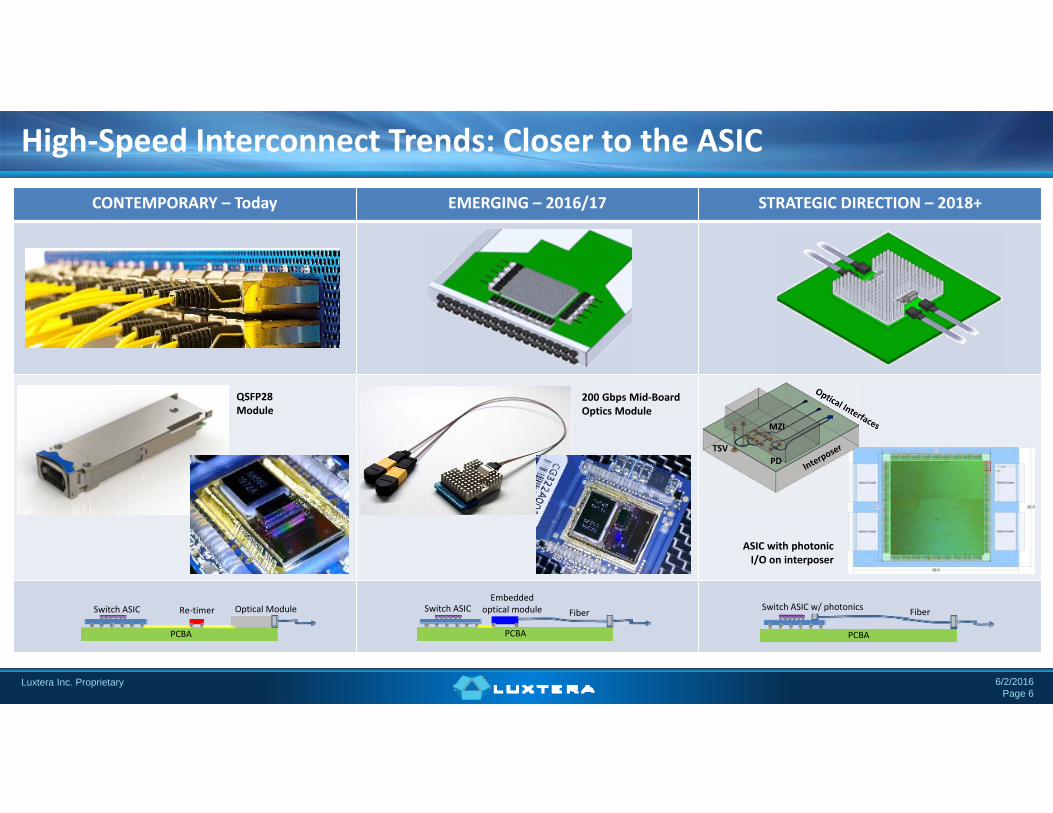
High‐Speed Interconnect Trends: Closer to the ASIC
Luxtera Inc. Proprietary 6/2/2016Page 6
CONTEMPORARY – Today EMERGING – 2016/17 STRATEGIC DIRECTION – 2018+
Embedded optical module FiberSwitch ASIC
PCBA
FiberSwitch ASIC w/ photonics
PCBA
Switch ASIC Re‐timer Optical Module
PCBA
ASIC with photonic I/O on interposer
QSFP28 Module
200 Gbps Mid‐Board Optics Module
TSV
MZI
PD

200 & 300 mm processes in two fabs:• Monolithic or hybrid integration of photonics with electronics• Qualified device libraries
Silicon Photonics Wafer Processing
Luxtera Inc. Proprietary 6/2/2016Page 7
Wafer processing:• Silicon on Insulator substrate (SOI)• Litho and etch of photonic structures• Implants for active devices• Selective Ge epitaxy for photo‐detectors• Standard BEOL
Transistor Passive Waveguide Phase Modulator Photo‐Detector

• Most transceiver applications need the light source to be integrated inside the module
• Si Photonics offers ability of using a remote light source
• Standard InP laser diode in a silicon micro package (incorporates many “lessons learned”): − Use mature InP laser diode technology− Include an optical isolator in the system− Use efficient coupling scheme− Wafer level assembly, packaging burn‐
in and test• Several versions developed:
− 1490 nm standard power− 1490 nm high power− 1310 nm high power
Light Source for Silicon Photonics: LaMP
Luxtera Inc. Proprietary 6/2/2016Page 8

Integration Photonics & Electronics
Luxtera Inc. Proprietary 6/2/2016Page 9
Monolithic Integration• Single chip solution• Lower parasitics between photonics and
electronics• More complex wafer fabrication process • Less area efficient• Moving to advanced nodes is complicated &
very expensive
Hybrid Integration• Multi chip solution• Higher parasitics between photonic and electronics• Photonics & electronics fabrication processes decoupled• Efficient use of area: photonics doesn’t take area on (expensive)
advanced e‐node• Flexible electronic node selection (CMOS, BiCMOS,..), enabling
integration with 3rd party IPMonolithic SiP IC
Electronics + Photonics
Photonic IC
Micro‐bumps
Electronic IC

Manufacturing flow for wafer level assembly & test
Luxtera Inc. Proprietary 6/2/2016Page 10
E‐Wafer WAT O‐Wafer WAT
Optical Probe
Plating
Plating E ‐ Probe
Dice
Assembly CoW
Assembly LoCoW
E‐Probe
E ‐ Probe
Dice

• Technology developed by multiple OSATs• Leverages technology developed for semiconductor electronics industry
• Enables electrical interconnect:− High density: pitch ~ 50 micron− Low parasitics− Wafer level assembly & test
Wafer Scale Assembly: Chip to wafer bonding of electronic IC
Luxtera Inc. Proprietary 6/2/2016Page 11

• Based on commercial pick‐and place tool• High throughput thanks to:− Fast active alignment− Fast adhesive curing− Wafer level assembly
• Built‐in process monitoring
Wafer Scale Assembly: Light Source to Wafer Bonding
Luxtera Inc. Proprietary 6/2/2016Page 12

• Optical & Electrical loop backs:
Wafer Level Assembly allows full optical BIST of transceiver engine
Luxtera Inc. Proprietary 6/2/2016Page 13
• Hybrid Architecture and Wafer Level Optical Assembly allow greater overall test coverage‒ Electrical & Optical sort performed on photonics die ‒ Electrical sort performed on electronics die Isolated testing of key analog blocks
‒ Final CoC assembly electrical testing with laser power
• High‐Speed Electrical loopback‒ Internal PRBS generation on TX‒ Loopback at E/O interface back to TIA/LA on the RX‒ Internal PRBS checker on the RX
• Hight‐Speed Optical loopback‒ Internal PRBS generation on TX‒ Loopback on optical interface back to replica PD and TIA on RX
‒ Internal PRBS checker on the RX
Fiber Array (16x 250u)
LaMP
LaMP
TX
RX
TX
RX
1
2
3
4
4
3
2
1
5
6
7
8
8
7
6
5

4x26 Gbps PSM‐4 Chipset & QSFP28 Module
Luxtera Inc. Proprietary 6/2/2016Page 14
Chipset mounted on PCBA:• Si Photonics IC (1310 nm)• Electronic IC (TSMC 28 nm)• Single light source (1310 nm)
Wire bonding for electrical connections:• High‐speed differential pairs• Power & ground• Low‐speed communication

8x28 Gbps PSM‐8 Chipset & 200 Gbps Module
Luxtera Inc. Proprietary 6/2/2016Page 15
Chipset mounted on PCBA:• Si Photonics IC (1310 nm)• Electronic IC (TSMC 28 nm)• Single light source (1310 nm)
Wire bonding for electrical connections:• High‐speed differential pairs• Power & ground• Low‐speed communication

Continued demand for increased data rates
– 400 G Ethernet– 200 G Ethernet– 50 G Ethernet
Data rate scaling: 100 G, 200 G, 400 G,…
6/2/2016Page 16
Data rate scaling vectors Silicon Photonics Technology
Technology platform:– Higher raw data rate: Library development
for 56Gbps NRZ and advanced modulation:o >50 GHz BW photo‐detectorso < 2 V.cm modulatorso General loss reductions
– Higher density: WDM, advanced modulation, multi‐core fiber
– Integration with Electronics/ASICs by 2.5 D integration
Advanced System and Circuit design:– Enhanced TX drivers, Enhanced RX
sensitivity– Advanced modulation– System control and monitoring– Advanced CMOS nodes (beyond 28 nm)– Integration with 3rd party IP
10
2614
56
12
48
NRZ
PAM‐4
Modulation
# WDM wavelengthsor fibers
Baud rate
Trade‐offs:– Cost– Power dissipation– Link budget margin– Scalability
Luxtera Inc. Proprietary

Advanced Transceiver Products• TSVs in photonic die (P die) eliminate power supply wire bonds to package
• TSVs allow lower parasitics for high speed interfaces• TSVs allow smaller form factor of assemblies• These improvements are beneficial for the next generation optical transceivers: 50 Gbps (NRZ) , 100 Gbps (50 Gbaud, PAM‐4)
Transition from Wire Bonding to Through‐Substrate Via (TSV)
SOC/ASIC Integration• Close integration of ASIC with photonics will revolutionize high speed interconnect
• Enables:– Drastic reduction in power dissipation by elimination of
electrical high speed I/Os– Drastic increase in density and reduction in form factor– Increase number of ports– Reduction in cost, by elimination of individual transceivers
• Form factor of SOC/ASIC chip assemblies is larger than those for transceiver products (full reticle or even larger)
6/2/2016Page 17
Luxtera Inc. Proprietary

www.luxtera.comLuxtera Proprietary
Acknowledgement:This presentation contains work of the entire Luxtera team and its technology partners, their
contributions are greatly acknowledged.
Thank you for your interest.