silicon carbide based transit time devices: the new frontier
TRANSCRIPT

Silicon Carbide Based Transit Time Devices: The New Frontier in High-power THz Electronics 143
X
Silicon Carbide Based Transit Time Devices: The New Frontier in High-power THz Electronics
Moumita Mukherjee
Centre of Millimeter-wave Semiconductor Devices and Systems, Institute of Radio Physics and Electronics,
University of Calcutta, India e-mail: [email protected]
1. Introduction
In recent years, the field of Terahertz (THz) science and technology has entered a completely new phase of unprecedented expansion that is generating ever-growing levels of broad-based international attention. Indeed, the plethora of activities that have arisen recently in both the technology and scientific arenas associated with the THz frequency domain - i.e., between 1 millimeter (300 GHz) and 100 micrometers (3 THz), suggest that the field might be attempting to undergo a dramatic transition that could lead to long-awaited payoffs in a number of application areas. The inherent advantages and potential payoffs of the THz regime for military & security as well as industry relevant applications have long stood as an important driver of interest in this science and technology area. This extremely expansive and spectrally unique portion of the EM spectrum had initial application in space-based communications, upper atmospheric sensing and potentially for short-range terrestrial communications and non-intrusive package screening. However, the very rapid growth in more recent years is arguably most closely linked to the potential payoffs of THz sensing and imaging for an array of military, security and industrial applications. These applications include the spectroscopic-based detection identification and characterization of chemical and biological agents and materials, remote and standoff early-warning for chemical-biological warfare threats, and imaging of concealed weapons and explosives, just to name a few. In addition, THz-regime finds its application possibilities in industry and private-sector areas as food-industry process control, pharmaceutical industry, biological science, medical diagnostics and security screening. Systems for rapidly emerging applications at THz frequencies thus require reliable high-power sources. In the last few years, the development of suitable sources for this frequency regime is being extensively explored worldwide. There are broadly two technology roadmaps for THz semiconductor devices. Approaching from the lower frequency range in the THz regime, electronic devices such as, Gunn diode, Resonant Tunneling diode (RTD) and nanometer Field Effect Transistors (FET) based on plasma wave have been widely investigated for THz frequency generation. From higher portion of the THz frequency spectrum, the photonics-based device Quantum Cascade Laser (QCL) extends the emission
7
www.intechopen.com

Properties and Applications of Silicon Carbide144
wavelength to Terahertz spectral range. The other approach to THz generation is through femtosecond lasers incident on materials with non-linear optical properties or on photoconductors such as InP. Parametric amplifiers are also being used for the purpose. All the above efforts are to pursue the effective generation of THz signals. Most of the available THz sources are complex and bulky. QCL, on the other hand, has the advantage of small size, though they require low temperature operation to directly generate THz. Thus it seems that there is lack of availability of small-sized suitable THz source to serve a useful purpose. So, the development of high-power, low-cost and compact semiconductor sources in THz regime has attracted the recent attention of researchers working in this field. Nowadays two-terminal solid-state Avalanche Transit-Time (ATT) devices are finding increasing applications in advanced RADAR, missile seekers and MM-wave communication systems. The performance of conventional Si (Silicon) and GaAs (Gallium Arsenide)-based IMPact ionization Avalanche Transit Time (IMPATT) devices are limited by power, operating temperature and especially by operating frequency. Recently, there is a global demand for THz-frequency applications and this warrants a new class of IMPATT oscillators which would outclass conventional Si and GaAs IMPATTs. Investigations on the prospects of Wide Bandgap (WBG) semiconductor materials, particularly IV-IV SiC semiconductors, for developing devices for high-frequency, high-power and high-temperature applications have been started recently. Considering all the above facts, the author has made an attempt to study the THz-frequency characteristics of SiC-based IMPATT oscillators. In this Chapter, light will be thrown on the reliability and experimental feasibility of this new class of devices in the THz-region. Also, photo-sensitivity of these new classes of devices will be included in the chapter.
2. Importance of SiC as a base semiconductor material for IMPATT fabrication
2.1 Hexagonal SiC SiC is recognized as a semiconductor of great importance in electronic applications because of its distinct properties, the possibility of easy growth on a native oxide, and the presence of numerous polytypes [1-4]. Silicon carbide is made up of equal parts silicon and carbon. Both are period IV elements, so they will prefer a covalent bonding such as in the left figure. Also, each carbon atom is surrounded by four silicon atoms, and vice versa. This will lead to a highly ordered configuration, a single polarized crystal. However, whereas Si or GaAs has only one crystal structure, SiC has several. The SiC family of semiconductor contains the same semiconductor material grown in many polytypes. The most commonly grown SiC materials are 4H-SiC, 6H-SiC, 3C-SiC. SiC, although of varied polytypes, generally have high carrier saturation velocity and high thermal conductivity, which make them suitable for high-temperature (above 900K), high-frequency (Terahertz region) applications [5]. Table 1 compares four semiconductors: silicon, gallium arsenide, silicon carbide and gallium nitride. Gallium Nitride is included here since in some respects it is perhaps a better material than SiC. It is also of interest to combine GaN with SiC, though the big difference is the energy bandgap. Standard semiconductors have almost three times smaller bandgaps than the wide bandgap materials SiC and GaN. However, it is probably the ten times larger critical field for breakdown which makes the biggest difference. There are no large differences in the other parameters, except the high mobility of GaAs. Cree Research Inc. [6]
was the first commercial vendor of SiC wafers which are commercially available as 4–inch wafers of 4H-SiC. It is well known that SiC wafer quality deficiencies are delaying the realization of outstandingly superior 4H-SiC high-power semiconductor devices. While efforts to date have centered on eradicating micropipes, 4H-SiC wafers and epilayers also contain elementary screw dislocations in densities on the order of thousands per cm2, nearly 100 fold micropipe densities. While not nearly as detrimental to SiC device performances as micropipes, it was shown earlier that diodes containing elementary screw dislocations exhibit a 5% to 35% reduction in breakdown voltage, higher pre-breakdown reverse leakage current, softer reverse breakdown I-V knee and concentrated microplasmic breakdown current filaments when measured under DC testing conditions. At present, the micropipe densities have decreased to less than 1 cm-2 in 4-inch wafers. 4H- and 6H- are the easiest to grow and are usually epitaxially grown on a Si substrate. Nowadays the commonly used method to grow SiC epitaxial layer is the Chemical Vapor deposition (CVD) technique. It provides good structural quality and excellent doping control. Recent advances in crystal growth and thin film epitaxy of SiC, allow the development of high-quality layers. The cubic phase, 3C-SiC, however, is difficult to grow because of lack of a suitable substrate, thus it receives less attention. However, in recent years, there has been some little interest in 3C-SiC, resulting in both experimental and theoretical works. The most difficult to grow is 2H-SiC, because of its high formation energy. The most common donors in SiC are nitrogen (N) and phosphorous (P). N substitutes on C sites in the lattice, while P on Si sites. The most common acceptors are aluminum (Al) and boron (B) which substitutes on Si sites.
Table 1. Comparison of material parameters of different semiconductors SiC was considered to be a promising material for fabrication of IMPATT diodes for the first time in 1973 by Keys [7]. In 1998, Konstantinov et al. fabricated epitaxial p-n diodes in 4H-SiC with uniform avalanche multiplications and breakdown [8]. They have performed photo-multiplication measurements to determine electron and hole ionization rates. P-n
Semiconductor
Si GaAs 4H-SiC 3C-SiC WZ-GaN Diamond
Bandgap (Eg) (eV)
1.12 1.42 3.26 2.3 3.45 5.45
Electric Breakdown field (EC)(107 V.m-1)
3.0 4.0 30.0 22.0 50.0 100.0
Relative dielectric constant (εr)
11.9 13.1 9.7 9.72 8.9 5.5
Electron mobility (µn) (m2 V-1s-1)
0.15 0.85 0.10
0.08
0.125 0.22
Hole mobility (µp) (m2 V-1s-1)
0.04 0.03 0.011
0.004 0.085 0.085
Saturated drift velocity of electrons
(vsn) (105 ms-1)
1.0 1.2 2.0 2.0 2.5 2.7
Thermal Conductivity (K)
(Wm-1 K-1)
150.0 46.0 490.0 450.0 225.0 1200.0
www.intechopen.com

Silicon Carbide Based Transit Time Devices: The New Frontier in High-power THz Electronics 145
wavelength to Terahertz spectral range. The other approach to THz generation is through femtosecond lasers incident on materials with non-linear optical properties or on photoconductors such as InP. Parametric amplifiers are also being used for the purpose. All the above efforts are to pursue the effective generation of THz signals. Most of the available THz sources are complex and bulky. QCL, on the other hand, has the advantage of small size, though they require low temperature operation to directly generate THz. Thus it seems that there is lack of availability of small-sized suitable THz source to serve a useful purpose. So, the development of high-power, low-cost and compact semiconductor sources in THz regime has attracted the recent attention of researchers working in this field. Nowadays two-terminal solid-state Avalanche Transit-Time (ATT) devices are finding increasing applications in advanced RADAR, missile seekers and MM-wave communication systems. The performance of conventional Si (Silicon) and GaAs (Gallium Arsenide)-based IMPact ionization Avalanche Transit Time (IMPATT) devices are limited by power, operating temperature and especially by operating frequency. Recently, there is a global demand for THz-frequency applications and this warrants a new class of IMPATT oscillators which would outclass conventional Si and GaAs IMPATTs. Investigations on the prospects of Wide Bandgap (WBG) semiconductor materials, particularly IV-IV SiC semiconductors, for developing devices for high-frequency, high-power and high-temperature applications have been started recently. Considering all the above facts, the author has made an attempt to study the THz-frequency characteristics of SiC-based IMPATT oscillators. In this Chapter, light will be thrown on the reliability and experimental feasibility of this new class of devices in the THz-region. Also, photo-sensitivity of these new classes of devices will be included in the chapter.
2. Importance of SiC as a base semiconductor material for IMPATT fabrication
2.1 Hexagonal SiC SiC is recognized as a semiconductor of great importance in electronic applications because of its distinct properties, the possibility of easy growth on a native oxide, and the presence of numerous polytypes [1-4]. Silicon carbide is made up of equal parts silicon and carbon. Both are period IV elements, so they will prefer a covalent bonding such as in the left figure. Also, each carbon atom is surrounded by four silicon atoms, and vice versa. This will lead to a highly ordered configuration, a single polarized crystal. However, whereas Si or GaAs has only one crystal structure, SiC has several. The SiC family of semiconductor contains the same semiconductor material grown in many polytypes. The most commonly grown SiC materials are 4H-SiC, 6H-SiC, 3C-SiC. SiC, although of varied polytypes, generally have high carrier saturation velocity and high thermal conductivity, which make them suitable for high-temperature (above 900K), high-frequency (Terahertz region) applications [5]. Table 1 compares four semiconductors: silicon, gallium arsenide, silicon carbide and gallium nitride. Gallium Nitride is included here since in some respects it is perhaps a better material than SiC. It is also of interest to combine GaN with SiC, though the big difference is the energy bandgap. Standard semiconductors have almost three times smaller bandgaps than the wide bandgap materials SiC and GaN. However, it is probably the ten times larger critical field for breakdown which makes the biggest difference. There are no large differences in the other parameters, except the high mobility of GaAs. Cree Research Inc. [6]
was the first commercial vendor of SiC wafers which are commercially available as 4–inch wafers of 4H-SiC. It is well known that SiC wafer quality deficiencies are delaying the realization of outstandingly superior 4H-SiC high-power semiconductor devices. While efforts to date have centered on eradicating micropipes, 4H-SiC wafers and epilayers also contain elementary screw dislocations in densities on the order of thousands per cm2, nearly 100 fold micropipe densities. While not nearly as detrimental to SiC device performances as micropipes, it was shown earlier that diodes containing elementary screw dislocations exhibit a 5% to 35% reduction in breakdown voltage, higher pre-breakdown reverse leakage current, softer reverse breakdown I-V knee and concentrated microplasmic breakdown current filaments when measured under DC testing conditions. At present, the micropipe densities have decreased to less than 1 cm-2 in 4-inch wafers. 4H- and 6H- are the easiest to grow and are usually epitaxially grown on a Si substrate. Nowadays the commonly used method to grow SiC epitaxial layer is the Chemical Vapor deposition (CVD) technique. It provides good structural quality and excellent doping control. Recent advances in crystal growth and thin film epitaxy of SiC, allow the development of high-quality layers. The cubic phase, 3C-SiC, however, is difficult to grow because of lack of a suitable substrate, thus it receives less attention. However, in recent years, there has been some little interest in 3C-SiC, resulting in both experimental and theoretical works. The most difficult to grow is 2H-SiC, because of its high formation energy. The most common donors in SiC are nitrogen (N) and phosphorous (P). N substitutes on C sites in the lattice, while P on Si sites. The most common acceptors are aluminum (Al) and boron (B) which substitutes on Si sites.
Table 1. Comparison of material parameters of different semiconductors SiC was considered to be a promising material for fabrication of IMPATT diodes for the first time in 1973 by Keys [7]. In 1998, Konstantinov et al. fabricated epitaxial p-n diodes in 4H-SiC with uniform avalanche multiplications and breakdown [8]. They have performed photo-multiplication measurements to determine electron and hole ionization rates. P-n
Semiconductor
Si GaAs 4H-SiC 3C-SiC WZ-GaN Diamond
Bandgap (Eg) (eV)
1.12 1.42 3.26 2.3 3.45 5.45
Electric Breakdown field (EC)(107 V.m-1)
3.0 4.0 30.0 22.0 50.0 100.0
Relative dielectric constant (εr)
11.9 13.1 9.7 9.72 8.9 5.5
Electron mobility (µn) (m2 V-1s-1)
0.15 0.85 0.10
0.08
0.125 0.22
Hole mobility (µp) (m2 V-1s-1)
0.04 0.03 0.011
0.004 0.085 0.085
Saturated drift velocity of electrons
(vsn) (105 ms-1)
1.0 1.2 2.0 2.0 2.5 2.7
Thermal Conductivity (K)
(Wm-1 K-1)
150.0 46.0 490.0 450.0 225.0 1200.0
www.intechopen.com
Properties and Applications of Silicon Carbide146
junction diodes were fabricated from p+ -n0 -n+ epitaxial structures grown by vapor phase epitaxy (VPE); n0 and n+ layers were deposited on the p+ substrates. The substrates were oriented in (0001) crystal plane with a small off-orientation angle, 3.50 or lower. The photo-multiplication measurement revealed that impact ionization in 4H-SiC appears to be dominated by holes, a hole to electron ionization co-efficient ratio up to 40-50 was observed. This ionization rate asymmetry was related to band-structure effects, to the discontinuity of the conduction band or the electron momentum along the c-direction. The results had a qualitative agreement with earlier studies of impact ionization in 6H-SiC. In 6H-SiC also, electron impact ionization was strongly suppressed and that was contributed to the discontinuity of the electron energy spectrum in the conduction band. Earlier problems in SiC device development due to poor material quality and immature device processing techniques was greatly overcome with the availability of production-quality substrates and the progress made in the processing technology. Though excellent microwave performances were demonstrated in SiC MESFETs and Static Induction transistors (SIT) [9], no experimental work was reported for SiC IMPATT devices before 2000. First experimental success of 4H-SiC based pulsed mode IMPATT was achieved by Yuan et al. in the year 2001 [10]. The DC characteristics of the high-low diodes exhibited hard, sustainable avalanche breakdown, as required for IMPATT operation. The fabricated 75 µm diameter SiC diodes were found to oscillate at 7.75 GHz at a power level of 1 mW. However, the output power level was significantly lower than the expected simulated value. They pointed out that the low-power problem is related to the measurement systems, particularly the design of the bias line. Optimization of the microwave circuit, in which the diode is embedded, is very important to properly evaluate the device performance. Any dispute in circuit optimization causes severe reduction in output power level. Thus, Yuan et al. made a comment that the measured low power, as obtained by their group, does not reflect the true power capability of SiC IMPATT [10]. Vassilevski et al. also fabricated 4H-SiC based IMPATT [11]. Microwave pulsed power of 300 mW was measured at 10 GHz. Though a comparatively higher power level was achieved, the power conversion efficiency was found to be very low ~0.3%. To increase the output power level, Ono et al. later [12] introduced a highly resistive guard ring that surrounds the diode periphery. The advantage of this guard ring is to reduce the electric field at the p-n junction edge of the junction periphery. A high current can thus be supplied through the diode without any destruction. Output power of 1.8W at 11.93 GHz was obtained from their fabricated diode and which is to date the highest reported output power from 4H-SiC IMPATT diodes. Nevertheless this power level is much lower than that expected. To increase the output power level, the residual series resistance should be minimized. No theoretical or experimental works on lo-hi-lo type 4H-SiC-based diodes have been published by other workers. The author has first time investigated the prospects of such devices in THz-frequency region for the first time.
2.2 Cubic SiC As discussed earlier, the high breakdown field and high thermal conductivity of all the polytypes of SiC coupled with high operational junction temperatures, theoretically permit extremely high power densities and efficiencies to be realized in SiC devices. Among all the polytypes of SiC, from the technological point of view, cubic (β)-SiC has certain advantages over hexagonal (α)-SiC. Although small area SiC wafers are commercially available for 4H-SiC and 6H-SiC hexagonal polytypes, their cost is 1000 times higher than that of 6 Si
substrates. Moreover, device quality 4H-SiC and 6H-SiC wafers are produced mainly by bulk-crystallization, including a process involving high substrate temperature (> 20000 C). This high temperature growth forms high density channeled defects, known as micropipes in α-SiC. Presence of such high density defects micropipes in α-SiC is a major problem, as it greatly degrades the device quality. On the other hand, β-SiC appears as a potential candidate, since it can be grown at a lower temperature. As there is no suitable substrate for growth of β-SiC crystals, the alternative is to use Si wafers which exist with good surface crystalline quality and with large surface area free of defects. Hetero-epitaxial growth of β-SiC on Si is a possible solution to overcome the problem of micropipes present in α-SiC polytypes. Moreover, the growth of good-quality 3C-SiC epilayers on Si would make it a cheaper alternative to costly 6H-SiC and 4H-SiC commercial epilayers and also makes it compatible with present Si technology. Additionally the β-SiC/Si heterostructures hold the promise for developing novel SiC/Si heterojunction devices and monolithic circuits combining SiC and Si devices. Also, the temperature coefficient of breakdown voltage of a p-n junction formed in 3C-SiC shows a positive value. A positive temperature coefficient is highly desirable to prevent runaway if devices reach the breakdown point. This indicates that IMPATT diodes can possibly be made with β-SiC, because the positive temperature coefficient is the direct result of an impact ionization process, required for the IMPATT diodes. Despite all of its advantages, the prospect of 3C-SiC as a base material for IMPATT fabrication has still not been explored. For the first time, the authors have simulated 3C-SiC based Single Drift flat profile (p+ n n+) IMPATT diode and the corresponding DC and terahertz characteristics of the device are also reported here. The authors have deposited p and n type 3C-SiC epilayers on Si substrate by Rapid Thermal Processing Chemical Vapour Deposition (RTPCVD) technique at a growth temperature as low as 8000C. A p-n junction has been grown successfully and the characterization of the grown 3C-SiC film has been completed. The corresponding results are reported here.
3. SiC (both Hexagonal and Cubic) based THz IMPATT
3.1 Design Approach SiC IMPATT diodes are designed and optimized through a generalized double iterative simulation technique used for analysis of IMPATT action [13]. The fundamental device equations, i.e. the one-dimensional Poisson’s equation and the combined current continuity equations under steady-state conditions, have been numerically solved subject to appropriate boundary conditions, through an accurate and generalized double iterative computer algorithm. Iteration over the value and location of field maximum are carried out until the boundary conditions of electric field E(x) and normalized current density P(x) = [JP(x) – Jn(x)]/J0 profiles are satisfied at both the edges of diode active layer. The DC solution gives the electric field E(x) profile, normalized current density P(x) profile, the maximum electric field (Em), drift voltage drop (VD), breakdown voltage (VB) and avalanche zone width (xa). The breakdown voltage (VB) is calculated by integrating the spatial field profile over the total depletion layer width. The boundary conditions for current density profiles are fixed by assuming a high multiplication factor (Mn, p) ~ 106, since it is well known that, avalanche breakdown occurs in the diode junction when the electric field is large enough such that the charge multiplication factors (Mn, Mp) become infinite. The edges of the depletion layer are also determined accurately from the DC analysis.
www.intechopen.com

Silicon Carbide Based Transit Time Devices: The New Frontier in High-power THz Electronics 147
junction diodes were fabricated from p+ -n0 -n+ epitaxial structures grown by vapor phase epitaxy (VPE); n0 and n+ layers were deposited on the p+ substrates. The substrates were oriented in (0001) crystal plane with a small off-orientation angle, 3.50 or lower. The photo-multiplication measurement revealed that impact ionization in 4H-SiC appears to be dominated by holes, a hole to electron ionization co-efficient ratio up to 40-50 was observed. This ionization rate asymmetry was related to band-structure effects, to the discontinuity of the conduction band or the electron momentum along the c-direction. The results had a qualitative agreement with earlier studies of impact ionization in 6H-SiC. In 6H-SiC also, electron impact ionization was strongly suppressed and that was contributed to the discontinuity of the electron energy spectrum in the conduction band. Earlier problems in SiC device development due to poor material quality and immature device processing techniques was greatly overcome with the availability of production-quality substrates and the progress made in the processing technology. Though excellent microwave performances were demonstrated in SiC MESFETs and Static Induction transistors (SIT) [9], no experimental work was reported for SiC IMPATT devices before 2000. First experimental success of 4H-SiC based pulsed mode IMPATT was achieved by Yuan et al. in the year 2001 [10]. The DC characteristics of the high-low diodes exhibited hard, sustainable avalanche breakdown, as required for IMPATT operation. The fabricated 75 µm diameter SiC diodes were found to oscillate at 7.75 GHz at a power level of 1 mW. However, the output power level was significantly lower than the expected simulated value. They pointed out that the low-power problem is related to the measurement systems, particularly the design of the bias line. Optimization of the microwave circuit, in which the diode is embedded, is very important to properly evaluate the device performance. Any dispute in circuit optimization causes severe reduction in output power level. Thus, Yuan et al. made a comment that the measured low power, as obtained by their group, does not reflect the true power capability of SiC IMPATT [10]. Vassilevski et al. also fabricated 4H-SiC based IMPATT [11]. Microwave pulsed power of 300 mW was measured at 10 GHz. Though a comparatively higher power level was achieved, the power conversion efficiency was found to be very low ~0.3%. To increase the output power level, Ono et al. later [12] introduced a highly resistive guard ring that surrounds the diode periphery. The advantage of this guard ring is to reduce the electric field at the p-n junction edge of the junction periphery. A high current can thus be supplied through the diode without any destruction. Output power of 1.8W at 11.93 GHz was obtained from their fabricated diode and which is to date the highest reported output power from 4H-SiC IMPATT diodes. Nevertheless this power level is much lower than that expected. To increase the output power level, the residual series resistance should be minimized. No theoretical or experimental works on lo-hi-lo type 4H-SiC-based diodes have been published by other workers. The author has first time investigated the prospects of such devices in THz-frequency region for the first time.
2.2 Cubic SiC As discussed earlier, the high breakdown field and high thermal conductivity of all the polytypes of SiC coupled with high operational junction temperatures, theoretically permit extremely high power densities and efficiencies to be realized in SiC devices. Among all the polytypes of SiC, from the technological point of view, cubic (β)-SiC has certain advantages over hexagonal (α)-SiC. Although small area SiC wafers are commercially available for 4H-SiC and 6H-SiC hexagonal polytypes, their cost is 1000 times higher than that of 6 Si
substrates. Moreover, device quality 4H-SiC and 6H-SiC wafers are produced mainly by bulk-crystallization, including a process involving high substrate temperature (> 20000 C). This high temperature growth forms high density channeled defects, known as micropipes in α-SiC. Presence of such high density defects micropipes in α-SiC is a major problem, as it greatly degrades the device quality. On the other hand, β-SiC appears as a potential candidate, since it can be grown at a lower temperature. As there is no suitable substrate for growth of β-SiC crystals, the alternative is to use Si wafers which exist with good surface crystalline quality and with large surface area free of defects. Hetero-epitaxial growth of β-SiC on Si is a possible solution to overcome the problem of micropipes present in α-SiC polytypes. Moreover, the growth of good-quality 3C-SiC epilayers on Si would make it a cheaper alternative to costly 6H-SiC and 4H-SiC commercial epilayers and also makes it compatible with present Si technology. Additionally the β-SiC/Si heterostructures hold the promise for developing novel SiC/Si heterojunction devices and monolithic circuits combining SiC and Si devices. Also, the temperature coefficient of breakdown voltage of a p-n junction formed in 3C-SiC shows a positive value. A positive temperature coefficient is highly desirable to prevent runaway if devices reach the breakdown point. This indicates that IMPATT diodes can possibly be made with β-SiC, because the positive temperature coefficient is the direct result of an impact ionization process, required for the IMPATT diodes. Despite all of its advantages, the prospect of 3C-SiC as a base material for IMPATT fabrication has still not been explored. For the first time, the authors have simulated 3C-SiC based Single Drift flat profile (p+ n n+) IMPATT diode and the corresponding DC and terahertz characteristics of the device are also reported here. The authors have deposited p and n type 3C-SiC epilayers on Si substrate by Rapid Thermal Processing Chemical Vapour Deposition (RTPCVD) technique at a growth temperature as low as 8000C. A p-n junction has been grown successfully and the characterization of the grown 3C-SiC film has been completed. The corresponding results are reported here.
3. SiC (both Hexagonal and Cubic) based THz IMPATT
3.1 Design Approach SiC IMPATT diodes are designed and optimized through a generalized double iterative simulation technique used for analysis of IMPATT action [13]. The fundamental device equations, i.e. the one-dimensional Poisson’s equation and the combined current continuity equations under steady-state conditions, have been numerically solved subject to appropriate boundary conditions, through an accurate and generalized double iterative computer algorithm. Iteration over the value and location of field maximum are carried out until the boundary conditions of electric field E(x) and normalized current density P(x) = [JP(x) – Jn(x)]/J0 profiles are satisfied at both the edges of diode active layer. The DC solution gives the electric field E(x) profile, normalized current density P(x) profile, the maximum electric field (Em), drift voltage drop (VD), breakdown voltage (VB) and avalanche zone width (xa). The breakdown voltage (VB) is calculated by integrating the spatial field profile over the total depletion layer width. The boundary conditions for current density profiles are fixed by assuming a high multiplication factor (Mn, p) ~ 106, since it is well known that, avalanche breakdown occurs in the diode junction when the electric field is large enough such that the charge multiplication factors (Mn, Mp) become infinite. The edges of the depletion layer are also determined accurately from the DC analysis.
www.intechopen.com

Properties and Applications of Silicon Carbide148
The high-frequency analysis of the IMPATT diodes provide insight into the dynamic performance of the diodes. The range of frequencies exhibiting negative conductance of the diode can easily be computed by Gummel-Blue method [14]. From the DC field and current profiles, the spatially dependent ionization rates that appear in the Gummel-Blue equations are evaluated and fed as input data for the small-signal analysis. The edges of the depletion layer of the diode, which are fixed by the DC analysis, are taken as the starting and end points for the small-signal analysis. The spatial variation of high-frequency negative resistivity and reactivity in the depletion layer of the diode are obtained under small-signal conditions by solving two second order differential equations in R(x, ) and X(x, ). R(x, ω) and X(x, ω) are the real and imaginary part of diode impedance Z (x,), such that, Z (x,) = R(x, ω) + j X(x, ω). A modified Runge-Kutta method is used for numerical analysis. The total integrated diode negative resistance (ZR) and reactance (Zx) at a particular frequency (ω) and current density J0, are computed from numerical integration of the R(x) and X(x) profiles over the active space-charge layer. The diode total negative conductance (G) and susceptance (B) are calculated from the equations. The basic mechanism of optical control of IMPATT diode is that, the leakage current entering the depletion region of the reversed biased p-n junction of an un-illuminated IMPATT diode is only due to thermally generated electron-hole pairs and it is so small that the multiplication factors (M n , p) become very high. When optical radiation of suitable wavelength (photon energy hc/λ > Eg) is incident on the active layer of the device, the leakage current increases significantly due to photo-generation of charge carriers. The leakage current densities due to optically generated electrons and holes, Jns, ps ׀opt depend on the incident optical power according to the following equation : (Jns or Jps)opt = q η Popt/ Ahν, (1) where, η is quantum efficiency and A is the surface area over which absorption of incident optical power Popt takes place corresponding to photon energy hν (ν is the frequency of incident radiation). If recombination is neglected, a linear response of the avalanche breakdown can be assumed, and (Jns)opt or (Jps)opt would increase linearly with Popt over a particular range of wavelengths in which appreciable absorption takes place. The enhancement of the leakage current under optical illumination of the devices is manifested as the lowering of Mn,p. In order to assess the role of leakage currents in controlling the dynamic properties of IMPATT oscillators at THz frequency, simulation experiments were carried out on the effect of electron current multiplication factor, Mn , (keeping hole current multiplication factor Mp very high ~ 106) and Mp (keeping Mn very high ~ 106) on (i) the small-signal admittance characteristics, (ii) the negative resistivity profiles, (iii) quality factor at peak frequencies (Qp), (iv) device negative resistance at peak frequencies (-ZRP) and (v) maximum power output of DDR SiC (both 4H- and 6H-) IMPATTs.
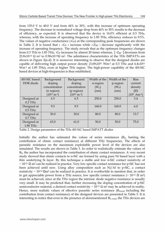
3.2 Results (Hexagonal SiC: un-illuminated diodes) The DC and small-signal properties of the designed diodes are shown in Table 2. The E(x) profiles of the THz DDR diodes are compared in Figure 1. It is found that the peak electric field (Em) increases from 4.25x10⁸ Vm-1 to 5.9x10⁸Vm-1, as the design frequency increases from 0.3 THz to 1.85 THz. The breakdown voltage and normalized voltage drop decrease
from 135.0 V to 40.0 V and from 44% to 30%, with this increase of optimum operating frequency. The decrease in normalized voltage drop from 44% to 30% results in the decrease of efficiency, as expected. It is observed that the device is 14.0% efficient at 0.3 THz, whereas, with the increase of operating frequency to 1.85 THz, efficiency reduces to 9.5%. The values of negative conductance (-GP) at the corresponding peak frequencies are shown in Table 2. It is found that ׀ –GP ׀ increase while ׀-ZRP ׀ decrease significantly with the increase of operating frequency. The study reveals that as the optimum frequency changes from 0.3 THz to 1.85 THz, -GP increases by almost 20 times whereas, -ZRP decreases from 23.8x10⁻¹⁰ Ω m2 to 0.58x10⁻¹⁰Ω m2. The admittance characteristics of the THz IMPATTs are shown in Figure 2(a-d). It is moreover interesting to observe that the designed diodes are capable of delivering high output power density (3.69x10¹¹ Wm-2 at 0.3 THz and 6.4x10¹¹ Wm-2 at 1.85 THz), even at higher THz region. The high-power capability of the 4H-SiC based devices at high-frequencies is thus established.
Table 2. Design parameters of the THz 4H-SiC based IMPATT diodes Initially the author has estimated the values of series resistances (RS, barring the contribution of ohmic contact resistance) at different THz frequencies. The effects of parasitic resistance on the maximum exploitable power level of the devices are also simulated. The results are shown in Table 3. In order to realistically estimate the values of RS, the author has incorporated the contribution of ohmic contact resistances. A very recent study showed that ohmic contacts to n-SiC are formed by using pure Ni based layer with a thin underlying Si layer. By this technique a stable and low n-SiC contact resistivity of ~ 10-11 Ω m2 can be realized in practice. Very low specific contact resistance for p-SiC has not been achieved until now. Using alloy composition such as Ni/Al to p-SiC, a contact resistivity ~ 10-10 Ωm2 can be realized in practice. It is worthwhile to mention that, in order to get appreciable power from a THz source, low specific contact resistance (~ 10-11 Ω m2) must be achieved, since at the THz region the intrinsic diode negative resistance is usually very small. It may be predicted that, further increasing the doping concentration of p-SiC semiconductor material, a desired contact resistivity ~ 10-11 Ω m2 may be achieved in reality. Hence, more realistic values of effective parasitic series resistance (RS,total including the contribution from contact resistance) of the designed devices are presented in Table 3. It is interesting to notice that even in the presence of aforementioned RS, total, the THz devices are
4H-SiC based DDR diode
Background doping
concentration (n region) (1023 m-3)
Background doping
concentration (p region) (1023 m-3)
Width of the n-region
(Wn) (nm)
Width of the p-region
(WP) (nm)
Bias current density
(J0) (109 Am-2)
Designed at 0.3 THz
6.5 6.5 250.0 250.0 3.4
Designed at 0.5 THz
9.5 9.5 160.0 160.0 6.0
Designed at 0.7 THz
30.0 30.0 80.0 80.0 13.7
Designed at 1.80 THz
63.0 61.0 50.0 50.0 75.0
www.intechopen.com
Silicon Carbide Based Transit Time Devices: The New Frontier in High-power THz Electronics 149
The high-frequency analysis of the IMPATT diodes provide insight into the dynamic performance of the diodes. The range of frequencies exhibiting negative conductance of the diode can easily be computed by Gummel-Blue method [14]. From the DC field and current profiles, the spatially dependent ionization rates that appear in the Gummel-Blue equations are evaluated and fed as input data for the small-signal analysis. The edges of the depletion layer of the diode, which are fixed by the DC analysis, are taken as the starting and end points for the small-signal analysis. The spatial variation of high-frequency negative resistivity and reactivity in the depletion layer of the diode are obtained under small-signal conditions by solving two second order differential equations in R(x, ) and X(x, ). R(x, ω) and X(x, ω) are the real and imaginary part of diode impedance Z (x,), such that, Z (x,) = R(x, ω) + j X(x, ω). A modified Runge-Kutta method is used for numerical analysis. The total integrated diode negative resistance (ZR) and reactance (Zx) at a particular frequency (ω) and current density J0, are computed from numerical integration of the R(x) and X(x) profiles over the active space-charge layer. The diode total negative conductance (G) and susceptance (B) are calculated from the equations. The basic mechanism of optical control of IMPATT diode is that, the leakage current entering the depletion region of the reversed biased p-n junction of an un-illuminated IMPATT diode is only due to thermally generated electron-hole pairs and it is so small that the multiplication factors (M n , p) become very high. When optical radiation of suitable wavelength (photon energy hc/λ > Eg) is incident on the active layer of the device, the leakage current increases significantly due to photo-generation of charge carriers. The leakage current densities due to optically generated electrons and holes, Jns, ps ׀opt depend on the incident optical power according to the following equation : (Jns or Jps)opt = q η Popt/ Ahν, (1) where, η is quantum efficiency and A is the surface area over which absorption of incident optical power Popt takes place corresponding to photon energy hν (ν is the frequency of incident radiation). If recombination is neglected, a linear response of the avalanche breakdown can be assumed, and (Jns)opt or (Jps)opt would increase linearly with Popt over a particular range of wavelengths in which appreciable absorption takes place. The enhancement of the leakage current under optical illumination of the devices is manifested as the lowering of Mn,p. In order to assess the role of leakage currents in controlling the dynamic properties of IMPATT oscillators at THz frequency, simulation experiments were carried out on the effect of electron current multiplication factor, Mn , (keeping hole current multiplication factor Mp very high ~ 106) and Mp (keeping Mn very high ~ 106) on (i) the small-signal admittance characteristics, (ii) the negative resistivity profiles, (iii) quality factor at peak frequencies (Qp), (iv) device negative resistance at peak frequencies (-ZRP) and (v) maximum power output of DDR SiC (both 4H- and 6H-) IMPATTs.
3.2 Results (Hexagonal SiC: un-illuminated diodes) The DC and small-signal properties of the designed diodes are shown in Table 2. The E(x) profiles of the THz DDR diodes are compared in Figure 1. It is found that the peak electric field (Em) increases from 4.25x10⁸ Vm-1 to 5.9x10⁸Vm-1, as the design frequency increases from 0.3 THz to 1.85 THz. The breakdown voltage and normalized voltage drop decrease
from 135.0 V to 40.0 V and from 44% to 30%, with this increase of optimum operating frequency. The decrease in normalized voltage drop from 44% to 30% results in the decrease of efficiency, as expected. It is observed that the device is 14.0% efficient at 0.3 THz, whereas, with the increase of operating frequency to 1.85 THz, efficiency reduces to 9.5%. The values of negative conductance (-GP) at the corresponding peak frequencies are shown in Table 2. It is found that ׀ –GP ׀ increase while ׀-ZRP ׀ decrease significantly with the increase of operating frequency. The study reveals that as the optimum frequency changes from 0.3 THz to 1.85 THz, -GP increases by almost 20 times whereas, -ZRP decreases from 23.8x10⁻¹⁰ Ω m2 to 0.58x10⁻¹⁰Ω m2. The admittance characteristics of the THz IMPATTs are shown in Figure 2(a-d). It is moreover interesting to observe that the designed diodes are capable of delivering high output power density (3.69x10¹¹ Wm-2 at 0.3 THz and 6.4x10¹¹ Wm-2 at 1.85 THz), even at higher THz region. The high-power capability of the 4H-SiC based devices at high-frequencies is thus established.
Table 2. Design parameters of the THz 4H-SiC based IMPATT diodes Initially the author has estimated the values of series resistances (RS, barring the contribution of ohmic contact resistance) at different THz frequencies. The effects of parasitic resistance on the maximum exploitable power level of the devices are also simulated. The results are shown in Table 3. In order to realistically estimate the values of RS, the author has incorporated the contribution of ohmic contact resistances. A very recent study showed that ohmic contacts to n-SiC are formed by using pure Ni based layer with a thin underlying Si layer. By this technique a stable and low n-SiC contact resistivity of ~ 10-11 Ω m2 can be realized in practice. Very low specific contact resistance for p-SiC has not been achieved until now. Using alloy composition such as Ni/Al to p-SiC, a contact resistivity ~ 10-10 Ωm2 can be realized in practice. It is worthwhile to mention that, in order to get appreciable power from a THz source, low specific contact resistance (~ 10-11 Ω m2) must be achieved, since at the THz region the intrinsic diode negative resistance is usually very small. It may be predicted that, further increasing the doping concentration of p-SiC semiconductor material, a desired contact resistivity ~ 10-11 Ω m2 may be achieved in reality. Hence, more realistic values of effective parasitic series resistance (RS,total including the contribution from contact resistance) of the designed devices are presented in Table 3. It is interesting to notice that even in the presence of aforementioned RS, total, the THz devices are
4H-SiC based DDR diode
Background doping
concentration (n region) (1023 m-3)
Background doping
concentration (p region) (1023 m-3)
Width of the n-region
(Wn) (nm)
Width of the p-region
(WP) (nm)
Bias current density
(J0) (109 Am-2)
Designed at 0.3 THz
6.5 6.5 250.0 250.0 3.4
Designed at 0.5 THz
9.5 9.5 160.0 160.0 6.0
Designed at 0.7 THz
30.0 30.0 80.0 80.0 13.7
Designed at 1.80 THz
63.0 61.0 50.0 50.0 75.0
www.intechopen.com

Properties and Applications of Silicon Carbide150
still capable of generating appreciable output power, as shown in Table 2. The effects of RS, total on the maximum power density of the devices are shown in Figure 3(a-d). It is very important to note that device negative resistances are much higher (at least 3.0 times) than the positive series resistance , which is an essential criteria for oscillations to take place. This observation also opens the prospect of 4H-SiC-based devices in the THz region.
4H-SiC based DDR diode Designed at 0.3 THz
Designed at 0.5 THz
Designed at 0.7 THz
Designed at 1.8 THz
Electric field maximum (Em) (108 V m-1)
4.25 4.30 5.25 5.9
Breakdown Voltage (VB) (V) 135.0 96.0 55.3 40.0 Normalized voltage drop
(VD/VB) (%) 44.0 37.7 32.97 30.0
Efficiency () (%) 14.0 12.0 10.5 9.5 Avalanche frequency (fa)
(THz) 0.170 0.425 0.6 1.2
Peak frequency (fP) (THz) 0.325 0.515 0.7 1.85 Negative conductance
(-Gp) (108 Sm-2) 1.62 2.90 7.4 32.0
Pmax (RS =0.0Ω) (1011 Wm-2)
3.69 3.34 2.82 6.4
Pmax (RS = RS, total) (1011 Wm-2)
3.37 2.9 2.5 5.75
Negative resistance (-ZRP) (10-10Ω m2)
23.8 7.3 3.8 0.58
-QP 1.26 1.95 1.6 2.15
Table 3. DC and Small-signal results of 4H-SiC based THz IMPATTs
Table 4. Estimation of Series resistance of the THz IMPATTs
4H-SiC DDR Diode
Negative conductance (-G) (108 Sm-2)
Susceptance (B)(108 Sm-2)
Estimated load
conductance (GL)(108Sm-2)
Negative resistance
(-ZR) (10-10Ωm2)
Series Resistance (RS)(10-10
Ωm2)
Total Series Resistance
(RS,total) (10-10 Ωm2)
Designed at 0.3 THz
1.53 1.50 1.30 33.4 10.2 (estimated at
0.3 THz)
10.40
Designed at 0.5 THz
2.75 3.00 2.42 16.60 3.66 (estimated at
0.5 THz)
3.86
Designed at 0.7 THz
7.4 12.0 6.7 3.8 0.49 (estimated at
0.7 THz)
0.69
Designed at 1.80 THz
27.0 30.0 26.8 1.66 0.022 (estimated at
1.5 THz)
0.22
The plots of variation of impedance of the diodes with frequencies are shown in Figure 4 (a-d). The graphs show that all the devices in the THz regime, posses negative resistance for all frequencies above the avalanche frequency (fa), where its reactance is capacitive. This is due to the fact that, in the oscillating frequency range, the magnitude of ZR is found to be small compared to ZX. Figures indicate that the values of |-ZR| and |-ZX| decrease as the operating frequency increases. The diode total negative resistance is thus an important parameter for designing a suitable THz device, as it determines the output power level and oscillation condition of the device. The simulation program has been used to obtain the negative resistivity profiles (R(x)) of the DDR diodes shown in Figure 5 (a-d). It is observed that the R(x) profile in each case is characterized by two negative resistivity peaks (Rmax) in the middle of the each drift layer along with a central negative resistivity minimum (Rmin) located near the metallurgical junction. The magnitudes of the two peaks in the electron and hole drift layers are found to decrease when the operating frequency increases. Thus the diode negative resistances,–ZRP, i.e. the area under the R(x) profiles, for the DDR diodes decrease very sharply with the increase of the frequency of operation. This observation is also reflected in Table 2, where the values of –ZRP are shown at different THz frequencies. Furthermore, the negative resistivity peaks produced by holes in the hole drift layers are appreciably higher than the peaks produced by electrons in the electron drift layers. Relative magnitudes of hole and electron ionization co-efficient in 4H-SiC at the operating electric field range are found to be correlated with the above effect. For practical realization of THz IMPATT, self-heating of the device is a major problem that will be discussed here. IMPATT devices are designed to be operated at a large current density in order to generate appreciable power in the THz region. It is found from the present simulation experiment, that the diodes are capable of generating high power density in the THz region. But, as the conversion efficiencies of the devices are within 10-14%, a small fraction of DC input power is converted into output power and the rest is dissipated as heat raising the junction temperature of the device. The optimized design however requires that the device will dissipate the power without increasing the junction temperature much over the ambient (300K), since the enhancement of junction temperature degrades the over-all performances of the THz devices. The safe operating temperature for Si (K=150 W m-1K-1) based IMPATT device is 573K. The value of K for SiC (490.0 W m-1K-1) is much higher (~ 3.3 times) than that of Si (Table 1). Hence, the SiC based IMPATT devices are expected to withstand much higher junction temperature, before they burn out. Thus the higher thermal conductivity allows 4H-SiC based devices to handle higher power. Moreover, if the SiC based THz diodes are mounted on a semi-infinite diamond (K Diamond = 1200 Wm-1K-1) heat-sink of much larger diameter as compared to the diameter of the device, the effective thermal conductivity will be very high and as a result it may be expected that the diode will be capable of dissipating the large amount of heat quickly from the junction, without increasing the junction temperature substantially. So the rise in junction temperature can be limited by proper heat-sink design and by using multiple mesas or ring geometry so that the thermal resistances of the diode and the heat-sink are reduced. The best way to resolve the self-heating problem is to operate the device under pulsed mode conditions with a small duty cycle so that the device does not heat up significantly and degrade in performance in the THz region.
www.intechopen.com

Silicon Carbide Based Transit Time Devices: The New Frontier in High-power THz Electronics 151
still capable of generating appreciable output power, as shown in Table 2. The effects of RS, total on the maximum power density of the devices are shown in Figure 3(a-d). It is very important to note that device negative resistances are much higher (at least 3.0 times) than the positive series resistance , which is an essential criteria for oscillations to take place. This observation also opens the prospect of 4H-SiC-based devices in the THz region.
4H-SiC based DDR diode Designed at 0.3 THz
Designed at 0.5 THz
Designed at 0.7 THz
Designed at 1.8 THz
Electric field maximum (Em) (108 V m-1)
4.25 4.30 5.25 5.9
Breakdown Voltage (VB) (V) 135.0 96.0 55.3 40.0 Normalized voltage drop
(VD/VB) (%) 44.0 37.7 32.97 30.0
Efficiency () (%) 14.0 12.0 10.5 9.5 Avalanche frequency (fa)
(THz) 0.170 0.425 0.6 1.2
Peak frequency (fP) (THz) 0.325 0.515 0.7 1.85 Negative conductance
(-Gp) (108 Sm-2) 1.62 2.90 7.4 32.0
Pmax (RS =0.0Ω) (1011 Wm-2)
3.69 3.34 2.82 6.4
Pmax (RS = RS, total) (1011 Wm-2)
3.37 2.9 2.5 5.75
Negative resistance (-ZRP) (10-10Ω m2)
23.8 7.3 3.8 0.58
-QP 1.26 1.95 1.6 2.15
Table 3. DC and Small-signal results of 4H-SiC based THz IMPATTs
Table 4. Estimation of Series resistance of the THz IMPATTs
4H-SiC DDR Diode
Negative conductance (-G) (108 Sm-2)
Susceptance (B)(108 Sm-2)
Estimated load
conductance (GL)(108Sm-2)
Negative resistance
(-ZR) (10-10Ωm2)
Series Resistance (RS)(10-10
Ωm2)
Total Series Resistance
(RS,total) (10-10 Ωm2)
Designed at 0.3 THz
1.53 1.50 1.30 33.4 10.2 (estimated at
0.3 THz)
10.40
Designed at 0.5 THz
2.75 3.00 2.42 16.60 3.66 (estimated at
0.5 THz)
3.86
Designed at 0.7 THz
7.4 12.0 6.7 3.8 0.49 (estimated at
0.7 THz)
0.69
Designed at 1.80 THz
27.0 30.0 26.8 1.66 0.022 (estimated at
1.5 THz)
0.22
The plots of variation of impedance of the diodes with frequencies are shown in Figure 4 (a-d). The graphs show that all the devices in the THz regime, posses negative resistance for all frequencies above the avalanche frequency (fa), where its reactance is capacitive. This is due to the fact that, in the oscillating frequency range, the magnitude of ZR is found to be small compared to ZX. Figures indicate that the values of |-ZR| and |-ZX| decrease as the operating frequency increases. The diode total negative resistance is thus an important parameter for designing a suitable THz device, as it determines the output power level and oscillation condition of the device. The simulation program has been used to obtain the negative resistivity profiles (R(x)) of the DDR diodes shown in Figure 5 (a-d). It is observed that the R(x) profile in each case is characterized by two negative resistivity peaks (Rmax) in the middle of the each drift layer along with a central negative resistivity minimum (Rmin) located near the metallurgical junction. The magnitudes of the two peaks in the electron and hole drift layers are found to decrease when the operating frequency increases. Thus the diode negative resistances,–ZRP, i.e. the area under the R(x) profiles, for the DDR diodes decrease very sharply with the increase of the frequency of operation. This observation is also reflected in Table 2, where the values of –ZRP are shown at different THz frequencies. Furthermore, the negative resistivity peaks produced by holes in the hole drift layers are appreciably higher than the peaks produced by electrons in the electron drift layers. Relative magnitudes of hole and electron ionization co-efficient in 4H-SiC at the operating electric field range are found to be correlated with the above effect. For practical realization of THz IMPATT, self-heating of the device is a major problem that will be discussed here. IMPATT devices are designed to be operated at a large current density in order to generate appreciable power in the THz region. It is found from the present simulation experiment, that the diodes are capable of generating high power density in the THz region. But, as the conversion efficiencies of the devices are within 10-14%, a small fraction of DC input power is converted into output power and the rest is dissipated as heat raising the junction temperature of the device. The optimized design however requires that the device will dissipate the power without increasing the junction temperature much over the ambient (300K), since the enhancement of junction temperature degrades the over-all performances of the THz devices. The safe operating temperature for Si (K=150 W m-1K-1) based IMPATT device is 573K. The value of K for SiC (490.0 W m-1K-1) is much higher (~ 3.3 times) than that of Si (Table 1). Hence, the SiC based IMPATT devices are expected to withstand much higher junction temperature, before they burn out. Thus the higher thermal conductivity allows 4H-SiC based devices to handle higher power. Moreover, if the SiC based THz diodes are mounted on a semi-infinite diamond (K Diamond = 1200 Wm-1K-1) heat-sink of much larger diameter as compared to the diameter of the device, the effective thermal conductivity will be very high and as a result it may be expected that the diode will be capable of dissipating the large amount of heat quickly from the junction, without increasing the junction temperature substantially. So the rise in junction temperature can be limited by proper heat-sink design and by using multiple mesas or ring geometry so that the thermal resistances of the diode and the heat-sink are reduced. The best way to resolve the self-heating problem is to operate the device under pulsed mode conditions with a small duty cycle so that the device does not heat up significantly and degrade in performance in the THz region.
www.intechopen.com

Properties and Applications of Silicon Carbide152
All the above observations are studied by the author for the first time and these definitely establish the prospects of 4H-SiC based devices in the THz regime, where conventional Si and GaAs diodes cannot perform.
Fig. 1. Electric field profiles of SiC THz IMPATTs
Fig. 2(a-d). Admittance plots of SiC THz IMPATTs within 0.3 – 1.8 THz
Fig. 3(a-d). Effects of series resistance on output power density of SiC THz IMPATTs within 0.3 – 1.8 THz (a: without Rs, b: with Rs)
www.intechopen.com

Silicon Carbide Based Transit Time Devices: The New Frontier in High-power THz Electronics 153
All the above observations are studied by the author for the first time and these definitely establish the prospects of 4H-SiC based devices in the THz regime, where conventional Si and GaAs diodes cannot perform.
Fig. 1. Electric field profiles of SiC THz IMPATTs
Fig. 2(a-d). Admittance plots of SiC THz IMPATTs within 0.3 – 1.8 THz
Fig. 3(a-d). Effects of series resistance on output power density of SiC THz IMPATTs within 0.3 – 1.8 THz (a: without Rs, b: with Rs)
www.intechopen.com

Properties and Applications of Silicon Carbide154
Fig. 4(a-d). Impedance plots of SiC THz IMPATTs within 0.3 – 1.8 THz.
Fig. 5(a-d). Negative resistivity profiles of SiC THz IMPATTs within 0.3 – 1.8 THz.
www.intechopen.com

Silicon Carbide Based Transit Time Devices: The New Frontier in High-power THz Electronics 155
Fig. 4(a-d). Impedance plots of SiC THz IMPATTs within 0.3 – 1.8 THz.
Fig. 5(a-d). Negative resistivity profiles of SiC THz IMPATTs within 0.3 – 1.8 THz.
www.intechopen.com

Properties and Applications of Silicon Carbide156
3.3 Results (Cubic SiC: Un-illuminated diode) The cubic (3C)-SiC based IMPATT diode has been optimized for low punch-through condition. Figure 6 shows the electric field profiles within the depletion layer of the p+ n n+ Terahertz IMPATT diode for the same bias current density (2 x10⁹ Am-2) and different active layer background doping concentration ranging from 0.7x1024 m-3 to 4x1024 m-3. The figure clearly indicates that the decrease in n-layer doping concentration increases the punch-through and decreases the maximum breakdown field. The corresponding efficiencies of the diodes at different doping densities are also shown in Figure 6. The efficiency (13%) is found to be higher for the diode structure showing lower punch through (background doping density = 4 x1024 m-3). The low punch through diode is found to be most efficient in the THz region. Thus, the DC and high frequency properties of the optimized low punch through diode are further simulated and the corresponding results are summarized in Table 2. The diode admittance plots, with and without RS , are shown in Figure 7 and they indicate that the diode negative conductance at 0.33 THz (peak operating frequency) will be 353.0 x10⁶ Sm-2. It is also observed from Figure 7 that in the presence of RS, the device negative conductance decreases significantly. The RF power output for the optimized device is found to be 63.0W at 0.33 THz. The parasitic series resistance for the 3C-SiC SDR diode was also determined and its effect on RF power is shown in Figure 8. It is evident from Figure 8 that due to the presence of RS, the CW power reduces by ~9%. The value of total negative resistance (-ZR) is found to be much higher than Rs at 0.3 THz, which is an essential condition for diode oscillation. Figure 9 shows the negative resistivity profile at the peak frequency for the optimized 3C-SiC SDR IMPATT device, with and without RS. Negative resistivity profiles give a physical insight into the region of the depletion layer that contributes to RF power. These figures show that for both the diode structures, the profiles exhibit negative resistivity peaks in the middle of the drift layer with dips in the avalanche layer close to the junction. The peak of the profile indicates that drift region contributes major role to higher negative resistance of the diode. Ellipsometry measurement reveals that Ge layers of thickness 300- 1000 A0 are formed on the Si substrate. The thickness of the SiC layer, as measured by ellipsometry is found to vary from 0.72 to 0.80 μm. The crystallinity of the doped films, studied by X-ray diffraction (XRD) technique, reveals that the SiC layers are perfectly crystalline (Figure 10). The peaks represent reflections from (left to right) Si (200), SiC (200), Si (400) and SiC (400) crystal planes. A Ge peak close to the SiC (400) peak is also observed. The angular positions of SiC (200), Si (400) and SiC (400) planes, as shown in the XRD spectrum match close with the corresponding angular position found by other researchers. The AFM pictures of the samples are shown in Figures 11 (a-b). Figure 11(a) reveals that there are large spots which are not visible, but these regions are visible for SiC layer grown on a Ge modified Si substrate (Figure 11(b)). Such large spots are indicative of holes or deeper lying parts on the SiC surface. Such features are connected with voids beneath the SiC layers. Therefore in the case of Ge pre-deposition the void formation is suppressed. Consequently the surface roughness of doped SiC film is found to be 16.0 nm, which is lower than the surface roughness of the film grown on Si surface without Ge pre-deposition. Transmission Electron Microscopy (TEM) measurement of sample without Ge incorporation is shown in Figure 12 (a). To improve the contrast of the TEM picture, the scale of the same sample in TEM mode is changed and shown in Figure 12 (b). In Figure 12(b), a comparison is made between TEM
measurements of samples with and without Ge incorporation. It is found that there is a noticeable improvement on the quality of SiC layer (Figure 12(b)). Scanning TEM of samples with Ge and without Ge are shown in Figure 13. It can be observed that Ge layer displaces a better contrast under STEM mode, as shown in Figure 13. Hence, it is expected that Ge layer acts as a barrier between Si/SiC interfaces, and prevents out-diffusion of substrate Si into the SiC films. These improvements are likely to reduce the leakage current flowing through the p-n junction. From Figure 14 it is observed that Ge-layer displays a better contrast under STEM mode (b). Figure 15 shows the SIMS profiling of doped 3C-SiC film on Si. It is evident that a clear p-n junction with doping concentration of 4.5 x 1024 atoms m-3 is formed, which is very close to the simulation data. The p-and n-layer thickness are (in μm) 1.38 and 0.472, respectively. The location of p-n junction is found to be 0.99μm. The location of Ge layer is 1.28 μm.
Fig. 6. Electric field profiles of 3C-SiC THz IMPATTs.
www.intechopen.com

Silicon Carbide Based Transit Time Devices: The New Frontier in High-power THz Electronics 157
3.3 Results (Cubic SiC: Un-illuminated diode) The cubic (3C)-SiC based IMPATT diode has been optimized for low punch-through condition. Figure 6 shows the electric field profiles within the depletion layer of the p+ n n+ Terahertz IMPATT diode for the same bias current density (2 x10⁹ Am-2) and different active layer background doping concentration ranging from 0.7x1024 m-3 to 4x1024 m-3. The figure clearly indicates that the decrease in n-layer doping concentration increases the punch-through and decreases the maximum breakdown field. The corresponding efficiencies of the diodes at different doping densities are also shown in Figure 6. The efficiency (13%) is found to be higher for the diode structure showing lower punch through (background doping density = 4 x1024 m-3). The low punch through diode is found to be most efficient in the THz region. Thus, the DC and high frequency properties of the optimized low punch through diode are further simulated and the corresponding results are summarized in Table 2. The diode admittance plots, with and without RS , are shown in Figure 7 and they indicate that the diode negative conductance at 0.33 THz (peak operating frequency) will be 353.0 x10⁶ Sm-2. It is also observed from Figure 7 that in the presence of RS, the device negative conductance decreases significantly. The RF power output for the optimized device is found to be 63.0W at 0.33 THz. The parasitic series resistance for the 3C-SiC SDR diode was also determined and its effect on RF power is shown in Figure 8. It is evident from Figure 8 that due to the presence of RS, the CW power reduces by ~9%. The value of total negative resistance (-ZR) is found to be much higher than Rs at 0.3 THz, which is an essential condition for diode oscillation. Figure 9 shows the negative resistivity profile at the peak frequency for the optimized 3C-SiC SDR IMPATT device, with and without RS. Negative resistivity profiles give a physical insight into the region of the depletion layer that contributes to RF power. These figures show that for both the diode structures, the profiles exhibit negative resistivity peaks in the middle of the drift layer with dips in the avalanche layer close to the junction. The peak of the profile indicates that drift region contributes major role to higher negative resistance of the diode. Ellipsometry measurement reveals that Ge layers of thickness 300- 1000 A0 are formed on the Si substrate. The thickness of the SiC layer, as measured by ellipsometry is found to vary from 0.72 to 0.80 μm. The crystallinity of the doped films, studied by X-ray diffraction (XRD) technique, reveals that the SiC layers are perfectly crystalline (Figure 10). The peaks represent reflections from (left to right) Si (200), SiC (200), Si (400) and SiC (400) crystal planes. A Ge peak close to the SiC (400) peak is also observed. The angular positions of SiC (200), Si (400) and SiC (400) planes, as shown in the XRD spectrum match close with the corresponding angular position found by other researchers. The AFM pictures of the samples are shown in Figures 11 (a-b). Figure 11(a) reveals that there are large spots which are not visible, but these regions are visible for SiC layer grown on a Ge modified Si substrate (Figure 11(b)). Such large spots are indicative of holes or deeper lying parts on the SiC surface. Such features are connected with voids beneath the SiC layers. Therefore in the case of Ge pre-deposition the void formation is suppressed. Consequently the surface roughness of doped SiC film is found to be 16.0 nm, which is lower than the surface roughness of the film grown on Si surface without Ge pre-deposition. Transmission Electron Microscopy (TEM) measurement of sample without Ge incorporation is shown in Figure 12 (a). To improve the contrast of the TEM picture, the scale of the same sample in TEM mode is changed and shown in Figure 12 (b). In Figure 12(b), a comparison is made between TEM
measurements of samples with and without Ge incorporation. It is found that there is a noticeable improvement on the quality of SiC layer (Figure 12(b)). Scanning TEM of samples with Ge and without Ge are shown in Figure 13. It can be observed that Ge layer displaces a better contrast under STEM mode, as shown in Figure 13. Hence, it is expected that Ge layer acts as a barrier between Si/SiC interfaces, and prevents out-diffusion of substrate Si into the SiC films. These improvements are likely to reduce the leakage current flowing through the p-n junction. From Figure 14 it is observed that Ge-layer displays a better contrast under STEM mode (b). Figure 15 shows the SIMS profiling of doped 3C-SiC film on Si. It is evident that a clear p-n junction with doping concentration of 4.5 x 1024 atoms m-3 is formed, which is very close to the simulation data. The p-and n-layer thickness are (in μm) 1.38 and 0.472, respectively. The location of p-n junction is found to be 0.99μm. The location of Ge layer is 1.28 μm.
Fig. 6. Electric field profiles of 3C-SiC THz IMPATTs.
www.intechopen.com

Properties and Applications of Silicon Carbide158
Fig. 7. Admittance plots of 3C-SiC THz IMPATT.
Fig. 8. Series resistance effects on RF power of 3C-SiC THz IMPATT.
Fig. 9. Series resistance effects on negative resistivity of 3C-SiC THz IMPATT.
. Fig. 10. XRD spectrum of β-SiC grown on Ge-modified Si <100> substrate.
www.intechopen.com

Silicon Carbide Based Transit Time Devices: The New Frontier in High-power THz Electronics 159
Fig. 7. Admittance plots of 3C-SiC THz IMPATT.
Fig. 8. Series resistance effects on RF power of 3C-SiC THz IMPATT.
Fig. 9. Series resistance effects on negative resistivity of 3C-SiC THz IMPATT.
. Fig. 10. XRD spectrum of β-SiC grown on Ge-modified Si <100> substrate.
www.intechopen.com

Properties and Applications of Silicon Carbide160
Fig. 11.(a) AFM picture taken from sample without Ge pre-deposition.
Fig. 11.(b) AFM picture taken from sample with Ge pre-deposition.
Fig. 12.(a) TEM micrograph of sample without Ge.
Fig. 12.(b) TEM micrographs of samples with Ge and without Ge.
www.intechopen.com

Silicon Carbide Based Transit Time Devices: The New Frontier in High-power THz Electronics 161
Fig. 11.(a) AFM picture taken from sample without Ge pre-deposition.
Fig. 11.(b) AFM picture taken from sample with Ge pre-deposition.
Fig. 12.(a) TEM micrograph of sample without Ge.
Fig. 12.(b) TEM micrographs of samples with Ge and without Ge.
www.intechopen.com

Properties and Applications of Silicon Carbide162
Fig. 13. Scanning-TEM of samples (a) with Ge & (b) without Ge. The arrow in Fig. 13(a) indicates a Ge layer formed at the interface of Si and 3C-SiC.
Fig. 14. 3C-SiC on Ge-modified Si: TEM and Scanning TEM analysis. Ge layer displays better contrast under STEM mode (figure 14(b))
Fig. 15. SIMS profile of β-SiC grown on Ge-modified Si <100> substrate.
3.3 Results (illuminated diodes) The effects of optical illumination on the THz behavior of the designed diode at 0.3 THz are shown in Figures 16 and 17. The computed values of –GP, -ZRP, Pmax, fP and –QP for different electron and hole current multiplication factors are shown there. Admittance plots of the SiC DDR IMPATT under the three different illumination conditions, as mentioned before, are shown in Figure 6. It is evident from the figures that the values of -GP at the optimum frequencies decrease with the lowering of Mn or Mp. At the same time, the frequency ranges over which the devices exhibit negative conductance, shift towards higher frequencies with the lowering of Mn and Mp. In the present calculation Mn and MP changes from 106 to 25, i.e. by a factor of 4x10⁴ due to photo-illumination, thus indicating an increase of leakage current by the same factor. The leakage current can be increased in reality by varying the incident optical power. Previous experiments on illuminated Si IMPATTs revealed that the leakage current increase from 1 nA to 500 µA, that is by a factor of 5x10⁵ by varying the incident optical power.
www.intechopen.com

Silicon Carbide Based Transit Time Devices: The New Frontier in High-power THz Electronics 163
Fig. 13. Scanning-TEM of samples (a) with Ge & (b) without Ge. The arrow in Fig. 13(a) indicates a Ge layer formed at the interface of Si and 3C-SiC.
Fig. 14. 3C-SiC on Ge-modified Si: TEM and Scanning TEM analysis. Ge layer displays better contrast under STEM mode (figure 14(b))
Fig. 15. SIMS profile of β-SiC grown on Ge-modified Si <100> substrate.
3.3 Results (illuminated diodes) The effects of optical illumination on the THz behavior of the designed diode at 0.3 THz are shown in Figures 16 and 17. The computed values of –GP, -ZRP, Pmax, fP and –QP for different electron and hole current multiplication factors are shown there. Admittance plots of the SiC DDR IMPATT under the three different illumination conditions, as mentioned before, are shown in Figure 6. It is evident from the figures that the values of -GP at the optimum frequencies decrease with the lowering of Mn or Mp. At the same time, the frequency ranges over which the devices exhibit negative conductance, shift towards higher frequencies with the lowering of Mn and Mp. In the present calculation Mn and MP changes from 106 to 25, i.e. by a factor of 4x10⁴ due to photo-illumination, thus indicating an increase of leakage current by the same factor. The leakage current can be increased in reality by varying the incident optical power. Previous experiments on illuminated Si IMPATTs revealed that the leakage current increase from 1 nA to 500 µA, that is by a factor of 5x10⁵ by varying the incident optical power.
www.intechopen.com

Properties and Applications of Silicon Carbide164
Fig. 16. Admittance plots of illuminated SiC THz IMPATTs at 0.3 THz.
Fig. 17. Negative resistivity profiles of illuminated SiC THz IMPATTs at 0.3 THz. Similar trends are observed in case of illuminated SiC THz IMPATTs at 0.5 THz, 0.7 THz and 1.85 THz.
4. Experimental feasibility
SiC epiwafer (n++ substrate and n-type epilayer) can be procured from Cree Inc., Durham, NC, USA. The n-type doping is usually realized at Cree using nitrogen gas as the precursor. A SiC IMPATT device can be fabricated on the epiwafer following the process steps described below and published elsewhere [M. Mukherjee, N. Mazumder and S. K. Roy 2008].
www.intechopen.com

Silicon Carbide Based Transit Time Devices: The New Frontier in High-power THz Electronics 165
Fig. 16. Admittance plots of illuminated SiC THz IMPATTs at 0.3 THz.
Fig. 17. Negative resistivity profiles of illuminated SiC THz IMPATTs at 0.3 THz. Similar trends are observed in case of illuminated SiC THz IMPATTs at 0.5 THz, 0.7 THz and 1.85 THz.
4. Experimental feasibility
SiC epiwafer (n++ substrate and n-type epilayer) can be procured from Cree Inc., Durham, NC, USA. The n-type doping is usually realized at Cree using nitrogen gas as the precursor. A SiC IMPATT device can be fabricated on the epiwafer following the process steps described below and published elsewhere [M. Mukherjee, N. Mazumder and S. K. Roy 2008].
www.intechopen.com

Properties and Applications of Silicon Carbide166
(i) Growth of p++ 4H-SiC layer: In order to assist p-type ohmic contact formation, the p++ 4H-SiC layer can be grown on top of the n-type film by Al2+ ion implantation; the doping concentration should be NA ≥ 2 x 1019 cm-3. The post-implantation annealing may be performed at ≈ 1600 º C for 45 minutes in argon atmosphere. (ii) Formation of low resistive p++ and n++ contacts: The power dissipation of IMPATT devices strongly depend on the contact resistance. Following step (i), the samples may be cleaned by a “piranha” solution. After rinsing in DI water, the samples may be dipped in dilute hydrofluoric (HF) acid solution for 30 seconds and dried. Immediately after the cleaning, a SiO2 layer on the p++ side can be grown by Plasma Enhanced Chemical Vapor Deposition (PECVD) at 2850C. Through photolithographic process, windows can be opened inside the oxide layer. Using photolithography and lift-off techniques, contact metals (Al/Ti/Al) can then be deposited in the oxide windows by an electron beam evaporator. In order to obtain ohmic contacts the samples may be annealed for 3 minutes in a Rapid Thermal Anneal (RTA) furnace in nitrogen atmosphere at 950 0C. The post-deposition annealing at high temperature is generally preferred to reduce the specific contact resistance. As mentioned in the literature, Ni is the preferred material for ohmic contact on n-type SiC (Roccaforte et al., 2006). Hence, for n++-type contact, a Ni layer of 200 nm thickness may be evaporated on the back-side (n++-side) of the wafer, followed by RTA treatment for 3 minutes at 950 0C. The choice of the metallic composition is based on the formation of Ni2Si alloy. As mentioned in several publications (Konishi et al, 2003), the higher the concentration of the Ni2Si in the contacts, the lower is the specific contact resistance. Finally, a composition of Ti/Au contact overlay is deposited on the p++-side by an electron beam evaporator. The specific contact resistance can be determined from transmission line measurement (TLM) data. (iii) The oxide layer from the p++-side can then be removed by Buffered Oxide Etch (BOE). (iv)Formation of diode mesa using Reactive Ion Etching (RIE): Si-C bonds show high chemical inertness, hence, wet etching is not efficient for reaching deep trenches. The more appropriate dry plasma etching, Reactive Ion Etching (RIE), may be used in separating the diode mesa. Patterning of mesas may be carried out with photoresists: AZ 5214 (standard) and TI 35 ES (special photoresist for deep RIE Si etching) (Lazar et al., 2006). A titanium/nickel (Ti/Ni) bilayer metal can be evaporated onto the sample. The metallic bilayer may be used as RIE mask that covers areas that will form mesa diodes. The dry etching can be performed in the Plasma Therm 790 reactor (say), an RIE reactor with a plasma (composed of SF6 and O2 gases) source generated at 13.56 MHz operating at a maximum power of 300W. The depth and etch rate of the mask may be determined by profilometry measurements with a Tencor Alpha Step. (v) On-Wafer DC Testing: After finishing the fabrication process, on-wafer DC testing are performed before the diodes are packaged. DC testing may serve as the initial screening step of the devices and the test results can be used for process evaluation. (vi)SiC IMPATT Device Packaging: The packaging should provide a low thermal resistance between the SiC diode chip and wave guide mount and should be mechanically rugged and hermetically sealed. The device can be bonded to a pill-type package. In pill-type configuration, the diode is bonded to a heat sink, which is usually gold plated. A ceramic or quartz ring encloses the diode and separates the heat sink from the package cap.
4.1 Terahertz transmission and measurement It is highly desirable that a THz transmission system should have low signal attenuation, low radiation loss, and high mode-confining property. Sommerfeld wires exhibit very low attenuation and dispersion, but suffers from large field extension into the surrounding medium. Moreover, it suffers from significant radiation loss at bendings. Metallic parallel plate waveguides, on the other hand, exhibit undistorted wave propagation of broadband sub-picosecond pulses even at bendings, but the propagating wave is confined in one transverse dimension giving rise to divergence loss. Transmission of THz signals from an IMPATT device may be possible with a dielectric coplanar wave guide, the device being an integral part of the waveguide. For THz (0.1-1 THz) signal transmission, a metallic slit waveguide, fabricated by sawing a 270 μm wide slit through a 140 mm wide and 300 μm thick silicon slabs may be used (Wachter et al., 2007). The metallic slit waveguide shows dispersion less transmission of THz signals with very low attenuation. However, the residual edge roughness from wafer sawing can cause a small degree of radiation loss. For higher frequency (3 THz) power transfer, a ribbon-like structure fabricated from ceramic alumina may be utilized (Yeh et al., 2005). Measurements of THz power and frequency may be done with a THz VNA (Vector Network Analyzer) or, by employing Photoconductive Method. In the Terahertz regime, vector network measurements are challenging because of the reduced wavelength. Also, large phase errors resulting from temperature fluctuation can occur. In addition, flexing of the cable linking the scanning waveguide probe to the measurement equipment adds to the phase uncertainty. There are other systems for measurement and detection of THz signals for example Hot Electron Bolometer mixer- receiver and THz Time Domain Spectroscopy (THz-TDS). For detection and measurement of THz beam by photoconductive method, a THz-TDS set-up may be used (Wachter et al, 2007). The photoconductive setup can avoid the input and output coupling of free space Terahertz beams, giving rise to a compact and versatile setup. THz Time Domain Spectroscopy measurement require multiple time delay scans, which is time consuming and can result in a systemic error caused by the intensity fluctuations of the THz beam. THz-TDS has smaller spectral range than Fourier Transform Spectroscopy (FTS) system and provide lower resolution than narrowband THz spectroscopy (Ferguson and Zhang, 2002).
5. Conclusion
It may be concluded that, the results reported here, reveal the potential of hexagonal and cubic -SiC IMPATTs as high-power THz source and the design may be used for experimental realization of SiC THz IMPATT. Based on the design, the authors have also successfully grown β-SiC p-n junction on Ge modified Si <100> substrate. Efforts have been made to reduce the lattice mismatch at Si/SiC interface by incorporating Ge. The preliminary results are encouraging and need further improvement to obtain 3C-SiC based IMPATTs with minimum reverse leakage current, additional results will be the subject of another paper.
www.intechopen.com

Silicon Carbide Based Transit Time Devices: The New Frontier in High-power THz Electronics 167
(i) Growth of p++ 4H-SiC layer: In order to assist p-type ohmic contact formation, the p++ 4H-SiC layer can be grown on top of the n-type film by Al2+ ion implantation; the doping concentration should be NA ≥ 2 x 1019 cm-3. The post-implantation annealing may be performed at ≈ 1600 º C for 45 minutes in argon atmosphere. (ii) Formation of low resistive p++ and n++ contacts: The power dissipation of IMPATT devices strongly depend on the contact resistance. Following step (i), the samples may be cleaned by a “piranha” solution. After rinsing in DI water, the samples may be dipped in dilute hydrofluoric (HF) acid solution for 30 seconds and dried. Immediately after the cleaning, a SiO2 layer on the p++ side can be grown by Plasma Enhanced Chemical Vapor Deposition (PECVD) at 2850C. Through photolithographic process, windows can be opened inside the oxide layer. Using photolithography and lift-off techniques, contact metals (Al/Ti/Al) can then be deposited in the oxide windows by an electron beam evaporator. In order to obtain ohmic contacts the samples may be annealed for 3 minutes in a Rapid Thermal Anneal (RTA) furnace in nitrogen atmosphere at 950 0C. The post-deposition annealing at high temperature is generally preferred to reduce the specific contact resistance. As mentioned in the literature, Ni is the preferred material for ohmic contact on n-type SiC (Roccaforte et al., 2006). Hence, for n++-type contact, a Ni layer of 200 nm thickness may be evaporated on the back-side (n++-side) of the wafer, followed by RTA treatment for 3 minutes at 950 0C. The choice of the metallic composition is based on the formation of Ni2Si alloy. As mentioned in several publications (Konishi et al, 2003), the higher the concentration of the Ni2Si in the contacts, the lower is the specific contact resistance. Finally, a composition of Ti/Au contact overlay is deposited on the p++-side by an electron beam evaporator. The specific contact resistance can be determined from transmission line measurement (TLM) data. (iii) The oxide layer from the p++-side can then be removed by Buffered Oxide Etch (BOE). (iv)Formation of diode mesa using Reactive Ion Etching (RIE): Si-C bonds show high chemical inertness, hence, wet etching is not efficient for reaching deep trenches. The more appropriate dry plasma etching, Reactive Ion Etching (RIE), may be used in separating the diode mesa. Patterning of mesas may be carried out with photoresists: AZ 5214 (standard) and TI 35 ES (special photoresist for deep RIE Si etching) (Lazar et al., 2006). A titanium/nickel (Ti/Ni) bilayer metal can be evaporated onto the sample. The metallic bilayer may be used as RIE mask that covers areas that will form mesa diodes. The dry etching can be performed in the Plasma Therm 790 reactor (say), an RIE reactor with a plasma (composed of SF6 and O2 gases) source generated at 13.56 MHz operating at a maximum power of 300W. The depth and etch rate of the mask may be determined by profilometry measurements with a Tencor Alpha Step. (v) On-Wafer DC Testing: After finishing the fabrication process, on-wafer DC testing are performed before the diodes are packaged. DC testing may serve as the initial screening step of the devices and the test results can be used for process evaluation. (vi)SiC IMPATT Device Packaging: The packaging should provide a low thermal resistance between the SiC diode chip and wave guide mount and should be mechanically rugged and hermetically sealed. The device can be bonded to a pill-type package. In pill-type configuration, the diode is bonded to a heat sink, which is usually gold plated. A ceramic or quartz ring encloses the diode and separates the heat sink from the package cap.
4.1 Terahertz transmission and measurement It is highly desirable that a THz transmission system should have low signal attenuation, low radiation loss, and high mode-confining property. Sommerfeld wires exhibit very low attenuation and dispersion, but suffers from large field extension into the surrounding medium. Moreover, it suffers from significant radiation loss at bendings. Metallic parallel plate waveguides, on the other hand, exhibit undistorted wave propagation of broadband sub-picosecond pulses even at bendings, but the propagating wave is confined in one transverse dimension giving rise to divergence loss. Transmission of THz signals from an IMPATT device may be possible with a dielectric coplanar wave guide, the device being an integral part of the waveguide. For THz (0.1-1 THz) signal transmission, a metallic slit waveguide, fabricated by sawing a 270 μm wide slit through a 140 mm wide and 300 μm thick silicon slabs may be used (Wachter et al., 2007). The metallic slit waveguide shows dispersion less transmission of THz signals with very low attenuation. However, the residual edge roughness from wafer sawing can cause a small degree of radiation loss. For higher frequency (3 THz) power transfer, a ribbon-like structure fabricated from ceramic alumina may be utilized (Yeh et al., 2005). Measurements of THz power and frequency may be done with a THz VNA (Vector Network Analyzer) or, by employing Photoconductive Method. In the Terahertz regime, vector network measurements are challenging because of the reduced wavelength. Also, large phase errors resulting from temperature fluctuation can occur. In addition, flexing of the cable linking the scanning waveguide probe to the measurement equipment adds to the phase uncertainty. There are other systems for measurement and detection of THz signals for example Hot Electron Bolometer mixer- receiver and THz Time Domain Spectroscopy (THz-TDS). For detection and measurement of THz beam by photoconductive method, a THz-TDS set-up may be used (Wachter et al, 2007). The photoconductive setup can avoid the input and output coupling of free space Terahertz beams, giving rise to a compact and versatile setup. THz Time Domain Spectroscopy measurement require multiple time delay scans, which is time consuming and can result in a systemic error caused by the intensity fluctuations of the THz beam. THz-TDS has smaller spectral range than Fourier Transform Spectroscopy (FTS) system and provide lower resolution than narrowband THz spectroscopy (Ferguson and Zhang, 2002).
5. Conclusion
It may be concluded that, the results reported here, reveal the potential of hexagonal and cubic -SiC IMPATTs as high-power THz source and the design may be used for experimental realization of SiC THz IMPATT. Based on the design, the authors have also successfully grown β-SiC p-n junction on Ge modified Si <100> substrate. Efforts have been made to reduce the lattice mismatch at Si/SiC interface by incorporating Ge. The preliminary results are encouraging and need further improvement to obtain 3C-SiC based IMPATTs with minimum reverse leakage current, additional results will be the subject of another paper.
www.intechopen.com

Properties and Applications of Silicon Carbide168
6. Acknowledgment
The author wishes to acknowledge (late) Prof. S. K. Roy, founder Director, CMSDS, University of Calcutta and (late) Prof. N. Mazumder, Professor, West Bengal University of Technology, for their support and keen interest in the work. The author is also grateful to Prof. Sanjay K. Banerjee, Director MRC, UT Austin, USA for providing experimental support. Thanks are also due to Seyoung Kim and Shagandeep Kour for their assistance in 3C-SiC layer growth and characterization. The assistance of Domingo Ferrer for TEM measurements is also gratefully acknowledged. The author also gratefully acknowledges DRDO (Defence Research and Development Organisation), Ministry of Defence, Govt. of India, and University Grants Commission (Govt. of India) for their financial support to carry out this work.
7. References
[1] Bhatnagar M ; and Baligla B, (1993) “Comparison of 6H-SiC, 3C-SiC, and Si for power devices,” IEEE Transactions on Electron Devices, vol. 40, no. 3, pp. 645–55.
[2] Weitzel, C.E ; Palmour, J. W ; Carter, J. C. H ; Moore, K. ; Nordquist, S ; Allen, C. Thero, and Bhatnagar, M ; (1996), “Silicon carbide high-power devices,”IEEE Transactions on Electron Devices, vol. 43, no. 10, pp. 1732–41.
[3] Cooper, J.A ; (1997) “Advances in SiC MOS technology,” Physica Status Solidi A, vol. 162, no. 1, pp. 305–320.
[4] Elasser A ; and Chow, T.P, (2002) “Silicon carbide benefits and advantages for power electronics circuits and systems,” Proceedings of the IEEE, vol. 90, no. 6, pp. 969–86.
[5] Ruff, M ; Mitlehner, H ; and Helbig, R ; (1994) “SiC devices: physics and numerical simulation,” IEEE Transactions on Electron Devices, vol. 41, no. 6, pp. 1040–54.
[6] www. Cree. Com [7] Keyes, R.W ; (1973) “Silicon Carbide from the prospective of physical limits on
semiconductor devices”, Proc. Silicon Carbide Conference: 1973, pp. 534 -542. [8] Konstantinov, A.O ; Waheb, Q ; Nordell N ; and Lindefelt, U ; (1998) “Ionization rates
and critical fields in 4H-SiC junction devices”, Mat. Sci. Forum, vol. 264 -268, pp. 513-515.
[9] Brandt, C.D ; Clarke, R.C ; Siergieg, R.C ; Casady, J.B ; Morse, A.W ; Sriram S ; and Agarwal, A. K ; “SiC for applications in high-power electronics”, in Semiconductors and Semimetals, Editor – Y. S. Park, New York, Academic, vol. 52, pp. 195 – 236, 1998.
[10] Yuan, L ; Copper, J.A ; Melloch M.R ; and Webb, K. J. (2001) “Experimental demonstration of a Silicon Carbide IMPATT oscillator”, IEEE Electron Device Letters, vol. 22, pp. 266 -268.
[11] Vassilevski, k ; Zorenko A ; et al., (2001) “4H-SiC IMPATT diode fabrication and testing”, Tech. Digest of Int. Conf. on SiC and Related Materials- ICSCRM, Tsukuba, Japan, p. 713, 2001.
[12] Ono, S ; Arai M ; and Kimura, C ; (2005) “Demonstration of high power X-band oscillation in p+ n - n+ 4H- SiC IMPATT diodes with guard-ring termination”, Materials Science Forum, Vol. 483-485, pp.981-984.
[13] Mukherjee M ; Mazumder N and Roy S. K ; (2008) “Photo-sensitivity analysis of GaN and SiC Terahertz IMPATT oscillators: comparason of theoretical reliability and study on experimental feasibility”, IEEE Trans. Device and Materials Reliability, vol. 8, p. 608.
[14] Gummel H.K ; and Blue, J. L. ; (1967) “A small signal theory of avalanche noise on IMPATT diodes”, IEEE Trans. Electron Devices, vol. ED -14, p. 569, 1967.
[15] F. Roccaforte, F. La Via, and V. Raineri, “SiC Materials and Devices; vol. 1, eds: M. Shur, S. Rumyantsev, and M. Levinshtein, World Scientific Publishing, p. 40, 2006.
[16] R. Konishi, R. Yasokuchi, O. Nakatsuka, Y. Koide, M. Moriyama, M Murakami “Development of Ni/Al and Ni/Ti/Al ohmic contact materials for p-type 4H-SiC” Mater. Sci. & Eng. B, vol. 98, pp. 286-293, 2003
[17] M. Lazar, H. Vang, P.Brosselard, C. Raynaud, P. Cremillieu, J.-L Leclercq, A.Descamps, S. Scharnholz, D. Planson,. “Deep SiC etching with RIE”, Supperlattices and Microstructures, vol. 40, pp. 388-392, 2006
[18] M. Wachter, M. Nagel and H. Kurz, “Metallic slit waveguide for dispersion-free low–loss terahertz signal transmission”, Applied Physics Letters, vol. 90, pp. 061111-061111-3, February 2007
[19] C. Yeh, F. Shimabukuro and P. H. Siegel, “ Low-loss terahertz ribbon waveguides”, Applied Optics, vol.44, No.28, pp. 5937-5946, October 2005
[20] M. Wachter, M. Nagel and H. Kurz, “Metallic slit waveguide for dispersion-free low–loss terahertz signal transmission”, Applied Physics Letters, vol. 90, pp. 061111-061111-3, February 2007
[21] B. Ferguson and X. Zhang, “Materials for THz science and technology”, Nat. Matr, vol. 1, pp.26-33, 2002.
www.intechopen.com

Silicon Carbide Based Transit Time Devices: The New Frontier in High-power THz Electronics 169
6. Acknowledgment
The author wishes to acknowledge (late) Prof. S. K. Roy, founder Director, CMSDS, University of Calcutta and (late) Prof. N. Mazumder, Professor, West Bengal University of Technology, for their support and keen interest in the work. The author is also grateful to Prof. Sanjay K. Banerjee, Director MRC, UT Austin, USA for providing experimental support. Thanks are also due to Seyoung Kim and Shagandeep Kour for their assistance in 3C-SiC layer growth and characterization. The assistance of Domingo Ferrer for TEM measurements is also gratefully acknowledged. The author also gratefully acknowledges DRDO (Defence Research and Development Organisation), Ministry of Defence, Govt. of India, and University Grants Commission (Govt. of India) for their financial support to carry out this work.
7. References
[1] Bhatnagar M ; and Baligla B, (1993) “Comparison of 6H-SiC, 3C-SiC, and Si for power devices,” IEEE Transactions on Electron Devices, vol. 40, no. 3, pp. 645–55.
[2] Weitzel, C.E ; Palmour, J. W ; Carter, J. C. H ; Moore, K. ; Nordquist, S ; Allen, C. Thero, and Bhatnagar, M ; (1996), “Silicon carbide high-power devices,”IEEE Transactions on Electron Devices, vol. 43, no. 10, pp. 1732–41.
[3] Cooper, J.A ; (1997) “Advances in SiC MOS technology,” Physica Status Solidi A, vol. 162, no. 1, pp. 305–320.
[4] Elasser A ; and Chow, T.P, (2002) “Silicon carbide benefits and advantages for power electronics circuits and systems,” Proceedings of the IEEE, vol. 90, no. 6, pp. 969–86.
[5] Ruff, M ; Mitlehner, H ; and Helbig, R ; (1994) “SiC devices: physics and numerical simulation,” IEEE Transactions on Electron Devices, vol. 41, no. 6, pp. 1040–54.
[6] www. Cree. Com [7] Keyes, R.W ; (1973) “Silicon Carbide from the prospective of physical limits on
semiconductor devices”, Proc. Silicon Carbide Conference: 1973, pp. 534 -542. [8] Konstantinov, A.O ; Waheb, Q ; Nordell N ; and Lindefelt, U ; (1998) “Ionization rates
and critical fields in 4H-SiC junction devices”, Mat. Sci. Forum, vol. 264 -268, pp. 513-515.
[9] Brandt, C.D ; Clarke, R.C ; Siergieg, R.C ; Casady, J.B ; Morse, A.W ; Sriram S ; and Agarwal, A. K ; “SiC for applications in high-power electronics”, in Semiconductors and Semimetals, Editor – Y. S. Park, New York, Academic, vol. 52, pp. 195 – 236, 1998.
[10] Yuan, L ; Copper, J.A ; Melloch M.R ; and Webb, K. J. (2001) “Experimental demonstration of a Silicon Carbide IMPATT oscillator”, IEEE Electron Device Letters, vol. 22, pp. 266 -268.
[11] Vassilevski, k ; Zorenko A ; et al., (2001) “4H-SiC IMPATT diode fabrication and testing”, Tech. Digest of Int. Conf. on SiC and Related Materials- ICSCRM, Tsukuba, Japan, p. 713, 2001.
[12] Ono, S ; Arai M ; and Kimura, C ; (2005) “Demonstration of high power X-band oscillation in p+ n - n+ 4H- SiC IMPATT diodes with guard-ring termination”, Materials Science Forum, Vol. 483-485, pp.981-984.
[13] Mukherjee M ; Mazumder N and Roy S. K ; (2008) “Photo-sensitivity analysis of GaN and SiC Terahertz IMPATT oscillators: comparason of theoretical reliability and study on experimental feasibility”, IEEE Trans. Device and Materials Reliability, vol. 8, p. 608.
[14] Gummel H.K ; and Blue, J. L. ; (1967) “A small signal theory of avalanche noise on IMPATT diodes”, IEEE Trans. Electron Devices, vol. ED -14, p. 569, 1967.
[15] F. Roccaforte, F. La Via, and V. Raineri, “SiC Materials and Devices; vol. 1, eds: M. Shur, S. Rumyantsev, and M. Levinshtein, World Scientific Publishing, p. 40, 2006.
[16] R. Konishi, R. Yasokuchi, O. Nakatsuka, Y. Koide, M. Moriyama, M Murakami “Development of Ni/Al and Ni/Ti/Al ohmic contact materials for p-type 4H-SiC” Mater. Sci. & Eng. B, vol. 98, pp. 286-293, 2003
[17] M. Lazar, H. Vang, P.Brosselard, C. Raynaud, P. Cremillieu, J.-L Leclercq, A.Descamps, S. Scharnholz, D. Planson,. “Deep SiC etching with RIE”, Supperlattices and Microstructures, vol. 40, pp. 388-392, 2006
[18] M. Wachter, M. Nagel and H. Kurz, “Metallic slit waveguide for dispersion-free low–loss terahertz signal transmission”, Applied Physics Letters, vol. 90, pp. 061111-061111-3, February 2007
[19] C. Yeh, F. Shimabukuro and P. H. Siegel, “ Low-loss terahertz ribbon waveguides”, Applied Optics, vol.44, No.28, pp. 5937-5946, October 2005
[20] M. Wachter, M. Nagel and H. Kurz, “Metallic slit waveguide for dispersion-free low–loss terahertz signal transmission”, Applied Physics Letters, vol. 90, pp. 061111-061111-3, February 2007
[21] B. Ferguson and X. Zhang, “Materials for THz science and technology”, Nat. Matr, vol. 1, pp.26-33, 2002.
www.intechopen.com

www.intechopen.com

Properties and Applications of Silicon CarbideEdited by Prof. Rosario Gerhardt
ISBN 978-953-307-201-2Hard cover, 536 pagesPublisher InTechPublished online 04, April, 2011Published in print edition April, 2011
InTech EuropeUniversity Campus STeP Ri Slavka Krautzeka 83/A 51000 Rijeka, Croatia Phone: +385 (51) 770 447 Fax: +385 (51) 686 166www.intechopen.com
InTech ChinaUnit 405, Office Block, Hotel Equatorial Shanghai No.65, Yan An Road (West), Shanghai, 200040, China
Phone: +86-21-62489820 Fax: +86-21-62489821
In this book, we explore an eclectic mix of articles that highlight some new potential applications of SiC anddifferent ways to achieve specific properties. Some articles describe well-established processing methods,while others highlight phase equilibria or machining methods. A resurgence of interest in the structural arena isevident, while new ways to utilize the interesting electromagnetic properties of SiC continue to increase.
How to referenceIn order to correctly reference this scholarly work, feel free to copy and paste the following:
Moumita Mukherjee (2011). Silicon Carbide Based Transit Time Devices: The New Frontier in High-power THzElectronics, Properties and Applications of Silicon Carbide, Prof. Rosario Gerhardt (Ed.), ISBN: 978-953-307-201-2, InTech, Available from: http://www.intechopen.com/books/properties-and-applications-of-silicon-carbide/silicon-carbide-based-transit-time-devices-the-new-frontier-in-high-power-thz-electronics

© 2011 The Author(s). Licensee IntechOpen. This chapter is distributedunder the terms of the Creative Commons Attribution-NonCommercial-ShareAlike-3.0 License, which permits use, distribution and reproduction fornon-commercial purposes, provided the original is properly cited andderivative works building on this content are distributed under the samelicense.