sideline: how delay-lines (may) leak secrets from your soc
TRANSCRIPT

SideLine: How Delay-Lines (May) Leak Secretsfrom your SoC
Joseph Gravellier1, Jean-Max Dutertre2, Yannick Teglia1, and Philippe LoubetMoundi1
1 Thales, La Ciotat, France{name.surname}@thalesgroup.com
2 Mines Saint-Etienne, CEA-Tech, Centre CMP. Gardanne, [email protected]
Abstract. To meet the ever-growing need for performance in silicon de-vices, SoC providers have been increasingly relying on software-hardwarecooperation. By controlling hardware resources such as power or clockmanagement from the software, developers earn the possibility to buildmore flexible and power efficient applications. Despite the benefits, thesehardware components are now exposed to software code and can poten-tially be misused as open-doors to new kind of attacks. In this work,we introduce SideLine, a novel side-channel vector based on delay-linecomponents widely implemented in high-end SoCs. We demonstrate thatthese entities can be used to perform remote power side-channel attacksand we detail several attack scenarios in which an adversary process lo-cated in one processor core aims at eavesdropping the activity of a victimprocess located in another core. For each scenario, we demonstrate theadversary ability to fully recover the secret key of an AES algorithmrunning in the victim core. Even more detrimental, we show that theseattacks are still practicable when a rich operating system is used.
1 Introduction
The need for direct physical access to a target to perform a hardware attackwas recently proved obsolete. Software-exposed hardware mechanisms imple-mented to improve SoC performance or power consumption were shown to besusceptible to remote hijacking by attackers seeking to perform fault injectionor Side-Channel Attacks (SCAs).
Since 2014, and the Rowhammer vulnerability’s disclosure [14], the remoteattack threat has become prevalent in hardware security researches. As a matterof fact, the influx of connected devices associated with the multiplication of cloudservices offers a new playing field for attackers. Moreover, despite the appearanceof trusted entities (ARM TrustZone, Intel SGX) that testify a growing need forSoC security, the hardware threat remains underestimated.
Between 2014 and today, Rowhammer capability evolved from random bitflips generation to privilege escalation on remote devices [12,17,32]. Meanwhile,the CLKSCREW exploit demonstrated that power and clock glitch attacks can
Author’s version Constructive Side-Channel Analysis and
Secure Design - COSADE 2021
DOI:10.1007/978-3-030-89915-8_1
arX
iv:2
009.
0777
3v2
[cs
.CR
] 2
Nov
202
1

2 J. Gravellier et al.
be launched from within an ARM SoC using software programmable voltage-frequency regulators [28]. Recently, this attack was improved [24] and deployedon Intel SGX devices [13,21]. From a side-channel point of view, two novel fami-lies of remote attacks have been introduced. On the one hand, micro-architecturaltiming attacks with Meltdown-Spectre [19,15], Foreshadow (SGX) [29] and morerecentlyMDS exploits [30,5]. These attacks leverage speculative and out-of-orderexecution in modern processors to steal secret data from victim processes. Onthe other hand, remote power SCAs have been introduced through several workson FPGA devices. Through the implementation of sensors inside a multi-userFPGA fabric, it was demonstrated that an adversary can eavesdrop the activityof the other users [26]. More recently, remote power SCAs have been extended tomicrocontroller devices using the ADCs they embed [10,22] and to Intel devicesusing the RAPL interface [18]. This spreads further the threats posed by remoteSCAs from FPGA fabrics to general purpose microcontrollers as those found inusual connected devices.
In this paper we introduce SideLine, a novel side-channel vector based onthe intentional misuse of hardware resources available in high-end SoC devices.SideLine leverages delay-lines components embedded in SoCs that use externalmemory; it neither requires embedded reconfigurable logic (FPGA) nor ana-log circuitry (ADC). Two delay-line blocks namely delay-locked-loop and pro-grammable delay-block are hijacked to perform voltage measurements and mali-ciously used to conduct power SCAs on application processors (AP) and micro-controllers units (MCU). SideLine makes it possible for an attacker to performsoftware-induced hardware attacks without direct physical access to the target.Our contributions are listed below:
• We reveal that delay-line-based components available in a broad range ofSoCs that employ external memories can be turned into power consumptionmeasurement units.
• We describe three attacker-victim (core-vs-core) delay-line-based SCA sce-narios over two SoC devices:AP-vs-AP attack (on a Xilinx Zynq 7000 SoC),AP-vs-MCU attack and MCU-vs-AP attack (on a STMicroelectronicsSTM32MP1 SoC) where AP and MCU respectively denote the applicationprocessor and the microcontroller.
• For each scenario a correlation power analysis attack is conducted againstthe publicly available OpenSSL AES encryption algorithm and the full secretkey is successfully recovered. The attack feasibility is demonstrated on baremetal and Linux OS-based applications.
Responsible Disclosure: We responsibly disclosed our findings to Xilinxon September 22th, 2020 and STMicroelectronics on November 2nd, 2020. Bothacknowledged and agreed on the publication of these results. Moreover, thisdisclosure led to a close collaboration with these companies to find and buildefficient countermeasures against SideLine and similar attacks. Please keep inmind that SideLine has been performed on these two processors for demonstra-tion purposes but the concept is generic and any devices that embed delay-linescan be affected.
SideLine 3
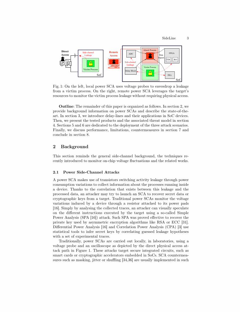
Fig. 1: On the left, local power SCA uses voltage probes to eavesdrop a leakagefrom a victim process. On the right, remote power SCA leverages the target’sresources to monitor the victim process leakage without requiring physical access.
Outline: The remainder of this paper is organized as follows. In section 2, weprovide background information on power SCAs and describe the state-of-the-art. In section 3, we introduce delay-lines and their applications in SoC devices.Then, we present the tested products and the associated threat model in section4. Sections 5 and 6 are dedicated to the deployment of the three attack scenarios.Finally, we discuss performance, limitations, countermeasures in section 7 andconclude in section 8.
2 Background
This section reminds the general side-channel background, the techniques re-cently introduced to monitor on-chip voltage fluctuations and the related works.
2.1 Power Side-Channel Attacks
A power SCA makes use of transistors switching activity leakage through powerconsumption variations to collect information about the processes running insidea device. Thanks to the correlation that exists between this leakage and theprocessed data, an attacker may try to launch an SCA to recover secret data orcryptographic keys from a target. Traditional power SCAs monitor the voltagevariations induced by a device through a resistor attached to its power pads[16]. Simply by analysing the collected traces, an attacker can visually speculateon the different instructions executed by the target using a so-called SimplePower Analysis (SPA [16]) attack. Such SPA was proved effective to recover theprivate key used by asymmetric encryption algorithms like RSA or ECC [31].Differential Power Analysis [16] and Correlation Power Analysis (CPA) [3] usestatistical tools to infer secret keys by correlating guessed leakage hypotheseswith a set of experimental traces.
Traditionally, power SCAs are carried out locally, in laboratories, using avoltage probe and an oscilloscope as depicted by the direct physical access at-tack path in Figure 1. These attacks target secure integrated circuits, such assmart cards or cryptographic accelerators embedded in SoCs. SCA countermea-sures such as masking, jitter or shuffling [34,36] are usually implemented in such

4 J. Gravellier et al.
secure devices. It encourages the use of high resolution and high sampling rateoscilloscopes on the attacker side to outperform the countermeasures.
Because traditional hardware attacks are assumed local and expensive, alarge number of electronic devices are not prepared to withstand remote hard-ware attack scenarios. For this reason, even with limited performances, digitaland analog integrated sensors may manage to jeopardize the security of devicesranging from IoT components to cloud servers (remote access in Figure 1). Withthe advent of these software-induced hardware attacks that do not require eitherdirect physical access to the target or specific equipment, the alleged hardwareattack limitations are called into question or even removed.
2.2 On-Chip Voltage Sensing
Two families of sensors enable malicious on-chip voltage sensing: either delaysensors built with digital logic gates which aim at measuring fluctuations inthe power consumption through delay variations [37,38], or analog sensors us-ing ADCs usually embedded in MCUs [10,22]. Until this work, digital sensorsdedicated to SCAs have been exclusively implemented in FPGAs. Their avail-able programmable logic makes it possible to design and tune such delay sensorsin order to measure the power consumption of a device. We describe hereafterthe principles of these delay sensors as their working principle is similar to thedelay-line components we used.
Delay-based voltage sensors leverage a side-effect of voltage fluctuations overdigital logic behavior, which is the relationship between the time taken by asignal to propagate through a digital logic gate and the on-chip voltage level. Anincrease of the gate’s power supply translates into a shortening of its propagationdelay, and respectively a reduction of the voltage induces its increase [9]. As aresult, measuring the variations of the logic gates propagation delay providesan image of their voltage supply variations. Temperature and capacitive effectsalso play a significant part in its equation [9]. Unlike voltage, the propagationdelay can be directly measured using digital logic. Commonly used FPGA-basedsensors are the Ring-Oscillator (RO [37]) and the Time-to-Digital Converters(TDC [26]).
2.3 Related Works
In 2018, Schellenberg et al. demonstrated that FPGA-based sensors were pre-cise enough to be used for SCAs on public and secret cryptographic algorithms[26]. To enable this attack, the adversary (a TDC-based delay sensor and itscontrol logic for power supply measurement) and the victim (an AES hardwareencryption block) needed to be located within the same FPGA. We define it asan FPGA-to-FPGA attack. The associated threat model targets multi-userFPGA cloud services that may appear over the next few years [6]. The sameyear, Zhao et al. disclosed that power SCAs can be conducted on heterogeneousplatforms that include both an application processor and an FPGA fabric on thesame silicon die. As a proof of concept, they were able to successfully retrieve
SideLine 5
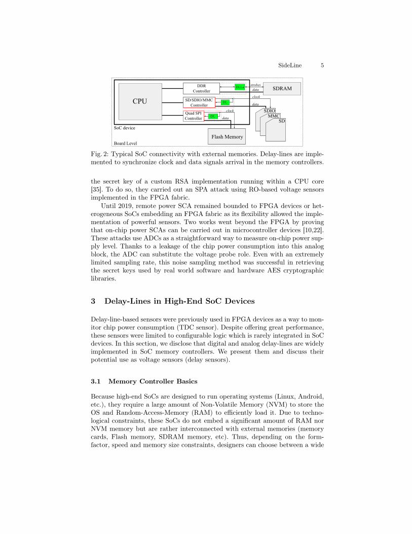
Fig. 2: Typical SoC connectivity with external memories. Delay-lines are imple-mented to synchronize clock and data signals arrival in the memory controllers.
the secret key of a custom RSA implementation running within a CPU core[35]. To do so, they carried out an SPA attack using RO-based voltage sensorsimplemented in the FPGA fabric.
Until 2019, remote power SCA remained bounded to FPGA devices or het-erogeneous SoCs embedding an FPGA fabric as its flexibility allowed the imple-mentation of powerful sensors. Two works went beyond the FPGA by provingthat on-chip power SCAs can be carried out in microcontroller devices [10,22].These attacks use ADCs as a straightforward way to measure on-chip power sup-ply level. Thanks to a leakage of the chip power consumption into this analogblock, the ADC can substitute the voltage probe role. Even with an extremelylimited sampling rate, this noise sampling method was successful in retrievingthe secret keys used by real world software and hardware AES cryptographiclibraries.
3 Delay-Lines in High-End SoC Devices
Delay-line-based sensors were previously used in FPGA devices as a way to mon-itor chip power consumption (TDC sensor). Despite offering great performance,these sensors were limited to configurable logic which is rarely integrated in SoCdevices. In this section, we disclose that digital and analog delay-lines are widelyimplemented in SoC memory controllers. We present them and discuss theirpotential use as voltage sensors (delay sensors).
3.1 Memory Controller Basics
Because high-end SoCs are designed to run operating systems (Linux, Android,etc.), they require a large amount of Non-Volatile Memory (NVM) to store theOS and Random-Access-Memory (RAM) to efficiently load it. Due to techno-logical constraints, these SoCs do not embed a significant amount of RAM norNVM memory but are rather interconnected with external memories (memorycards, Flash memory, SDRAM memory, etc). Thus, depending on the form-factor, speed and memory size constraints, designers can choose between a wide

6 J. Gravellier et al.
range of external memory devices. A typical scenario of a SoC using externalmemories is depicted in Figure 2.
Several memory controllers are required to interface the SoC with its exter-nal memories. Each memory controller acts as a request arbiter, a transactionscheduler and as a physical interface to manage data flowing from the SoC tothe memory, and vice-versa. In embedded systems, for cost and efficiency rea-sons, the memory controller is more likely to be directly integrated as a partof the SoC. At the edge of the memory controller, a physical controller (dot-ted lines in Figure 2) outputs and captures the signals that will flow betweenthe SoC I/Os and the memory device I/Os (clock, data, configuration signals,etc.). The physical controller also ensures that these signals arrive on time re-gardless of the interconnection tracks length on the PCB, the voltage and thetemperature variations. To better understand the extent of memory signal prop-agation timings, we draw a simple example of SoC/Synchronous Dynamic-RAM(SDRAM) association. When a read operation is initiated by the SoC, the ex-ternal SDRAM memory outputs the requested data edge-aligned with a clocksignal (strobe) later dedicated to data sampling. Depending on the PCB trackslength, the clock signal is likely to shift ahead of the data signals, leading then toa sampling error. To mitigate this effect, the SoC physical controller implementsdelay-line-based components (delay-locked-loop DLL and programmable delay-block DL in Figure 2) to calibrate the phase alignment between the samplingclock and the data signals. This calibration can be manual and made once andfor all after testing at manufacturing or performed at each chip power-up. It canalso be adjusted dynamically to counterbalance any misalignment due to powersupply or temperature fluctuations.
The relationship between the delay applied and the SoC voltage fluctuationsdrew our interest. In the following paragraphs, we present two different delay-line-based mechanisms that can be used to generate these delays for low andhigh-bandwidth external memory applications.
3.2 Delay-blocks in Low-Bandwidth Memory Controllers
In relatively low-bandwidth external memories such as Flash memories, SD cardsand multimedia cards, the impact of voltage and temperature fluctuations isconsidered not significant enough to jeopardize the communication integrity:dynamic calibration is not required. Delay-lines are nonetheless used to mitigatethe impact of the PCB track length on the data and clock signals propagationtimings (these delays are not predictable by SoC designers, they are set only atboard design time). As track lengths are fixed, a static delay is sufficient to ensuregood operation. For a read transaction, the delay-line is typically calibrated inorder to add a phase shift of 90◦ to the clock signal. Thus, it ensures thatdata signals are in place when sampling occurs. The delay-line calibration iscarried out through a series of training steps. These training steps modify thedelay of the elements forming the chain and, for each configuration, verify ifthe external memory has been properly read. If the training is successful, the

SideLine 7
Fig. 3: An example of delay-block used in low-bandwidth memory controllers.
delay-line configuration is saved in a dedicated register and remains unchangeduntil the next test.
Several SoC vendors provide user programmable delay-blocks as a way fordevelopers to be able to use a wide range of memory chips or cards with dif-ferent bus speeds. Unlike traditional static delay-lines, these delay-blocks comewith both a complete calibration toolkit and a detailed documentation. Figure3 illustrates the delay-block structure that was observed in one of the SoC webenchmarked. Its purpose is to delay the clock signal with respect to the datasignals when a read operation is conducted. The block consists in a simple delay-line associated with a set of control and status registers. A Command Registercontrols the delay t of all the delay-line elements and thus the phase shift addedto the clk signal. To ensure that the phase shift obtained is conform to the ap-plied command, a state register captures the output of each element forming thedelay-line every time a clkin rising edge event occurs. Then, a specific trainingis performed to verify whether the captured pattern matches the command ornot.
Despite some missing parts, this structure is reminiscent of that of a TDC asthe delay-line state is continuously captured and stored in an accessible register.In section 6, we demonstrate that this delay-block can be turned into a voltagesensor and hijacked to perform a power SCA.
3.3 DLLs in High-Bandwidth Memory Controllers
Because of the continuous increasing in memory bus speeds, the available slacktime for data sampling is gradually shrinking. Double data rate memories (DDR)such as SDRAM memory perform one data transfer per clock edge (both risingand falling) while reaching gigahertz frequencies [25]. On these devices, the datasampling is very likely to get corrupted by temperature and voltage variations.This time, a static delay source is not suitable to ensure correct operations. Toeffectively cancel voltage and temperature noise side-effects, a dynamic way toadapt the clock delay has to be considered.
Delay Locked Loops (DLLs) are generally used in recent DDR memory con-trollers to dynamically track and control the phase shift applied between thesampling clock and the external memory (e.g. SDRAM) data signals [2,7]. Asillustrated in Figure 4, a DLL has two main blocks: a delay-line, and a feedback

8 J. Gravellier et al.
Fig. 4: An example of delay-locked-loop used in DDR memory controllers.
circuit. The delay-line is calibrated to provide a phase shift to a clk signal us-ing both coarse and fine delay elements. However, the propagation delay jitterassociated with on-chip voltage and temperature fluctuations is likely to skewthe applied phase. This is why a DLL includes a feedback circuit to tune thedelay-line in order to provide a dynamic control of the phase shift and thus,counterbalance voltage and temperature variations. The feedback circuit comeswith a phase detector that compares the phase shift between the clock signalat the input of the delay-line, clkin, and its phase-shifted clock output, clkout.Then, according to the measured error, a delay controller applies a correction inorder to "deskew" the result, that is, to get back to the initial delay. The appliedcorrection modifies the delay of the elements forming the delay-line and can beeither analog or digital-controlled depending on the delay-line type [1].
A command register stores the delay settings, it is memory-mapped and hencecan be read from the SoC AP or MCU cores. The DLL operates autonomously,this means that through a simple access to this register, a process can retrieve thestate of the DLL, which shall be correlated to on-chip voltage and temperaturevariations. As a result, tracking the command register content shall provide animage of the SoC power consumption that may be used to carry out SCAs.Note that this measurement methodology (tracking the command of a feedbackdynamically controlled system) differs from that described in Section 3.2 fordelay-blocks (sampling a clock signal propagating inside a fixed delay-line). If thisunusual measurement medium provides enough resolution and sampling rate toeavesdrop power consumption of secure applications running on a processor, thiscould represent an important backdoor for computer security. This hypotheticalvulnerability is strengthened by the fact that this attack only requires a readaccess to the command register, no configuration steps are required. This attackscenario is developed in section 5.
4 Experimental Setup
4.1 Tested Devices
Two devices from two different SoC providers have been studied in our experi-ments. The first target considered in this work is a Xilinx Zynq-7000 SoC [33]that comes with a dual-core Cortex-A9 application processor (AP). It is a typical
SideLine 9
multi-purpose SoC providing many additional resources: FPGA, I/O, ADCs, buscontrollers, etc. It supports DDR2-DDR3, Flash and SD/MMC external mem-ories and provides several DLL blocks to interface properly with DDR externalmemories. The experiments made on this target have been conducted withoutusing an OS: we denote it as a bare metal attack. This configuration makesSCA easier as there are fewer interruptions (with respect to the case in whichan OS is used) that may disturb the attack and victim processes and cause syn-chronization issues. The entire Zynq-based SideLine attack code can be clonedfrom GitHub: https://github.com/Remote-HWA/SideLine_Zynq.
The second target is a STMicroelectronics STM32MP157C-DK2 developmentboard [20] that embeds a dual-core Cortex-A7 AP associated with a Cortex-Mprocessor (MCU). It also supports DDR2-DDR3, Flash and SD/MMC externalmemories and embeds several DLL blocks. Additionally, it provides user pro-grammable delay-blocks (DLYB [20]) that can be employed for interfacing lowbandwidth memory (e.g. an SD card). These programmable delay-blocks are thesecond case we studied. The experiments done on this SoC have been carriedout with a Linux OS running on its AP (i.e. the Cortex-A7 processor). The re-sults are those of a Linux OS attack. The entire STM32MP1-based SideLineattack code can be cloned from GitHub: https://github.com/Remote-HWA/SideLine_STM32MP1.
4.2 OpenSSL AES Architecture
The OpenSSL library [23] provides several cryptographic algorithms used for se-curing channels over computer networks. In this work, we focus on the OpenSSLAES-128 (version 1.1.1) that implements a 32-bit tabulated version of the text-book AES encryption algorithm [8]. This variant merges the Mixcolumn andSubBytes transformations into 4 pre-computed look-up tables known as T-tables(256 x 32-bit) as a way to optimize the computations on 32-bit processors.
4.3 Threat Model
In this work, we introduce three core-vs-core attack scenarios in order to assessthe SCA capabilities of the delay-line-based sensors. For each scenario depicted inFigure 5, we first deploy a cryptographic application (in green) within a processorcore. This application located either in the AP or in the MCU allows the end-userto launch AES encryptions/decryptions, with the plaintexts/ciphertexts that heprovides. Secondly, we introduce a malicious user (in red) that has the privilegelevel necessary to access the delay-line blocks presented in Section 3 and thatuses them to retrieve the leakage induced by the AES application.
Although not used in this research work, Trusted Execution Environment(TEE) and TrustZone [2] architecture stand as potential realistic targets forthe delay-lines. TrustZone attacks from the normal-world to the secure-worldhave been widely covered in recent remote attack works [28,24,4,22]. However,from a side-channel point of view, the current TrustZone does not provide any

10 J. Gravellier et al.
delay-locked loop
Power leakage
DLL command
ZYNQ-7000 SoC STM32MP1 SoC
MC
U
Victim Process
delay block
a) AP-vs-AP Attack b) MCU-vs-AP Attack c) AP-vs-MCU Attack
Power leakage
Power leakage
Attack Process Victim Process
AP#0 AP#1
Attack Process
delay block
AP#0 AP#1 AP#0 AP#1Attack Process
Victim Process
MC
UDelay Line state
Delay Line state
STM32MP1 SoC
Fig. 5: Basic principle of the three core-vs-core attack variants proposed in thiswork. It shows the leakage path from the victim process to the delay sensor andthe sensor data flow retrieved by the attack process.
countermeasures. Thus, the ability of an attacker to turn our feasibility attackinto an end-to-end TrustZone attack is reasonably expected.
In the remainder of the paper, the three scenarios presented are referred toas:
1. A DLL-based attack (Figure 5.a), or AP-vs-AP attack, that demonstratesthe ability of a DLL to serve as a power supply sensor suitable for a CPAattack against the AES algorithm. In this scenario, one core of the Zynqprocessor runs the AES victim application, while the second core executesthe attack process (both victim and aggressor processes are C programs, inbare metal mode). The attacker code is in charge of collecting the leakagedata of the AES. It does so by configuring the access to the DLL commandregister that makes it possible to sample its values during AES encryptionsperformed by the first core. The attacker core is also in charge of providingthe plaintext to be ciphered by the victim process and to trigger both theencryption and readback of DLL states. This AP-vs-AP attack scenario isdescribed in details in Section 5.
2. A first Delay-Block-based attack (Figure 5.b), or MCU-vs-AP attack,where the victim process is ran on the STM32MP1 AP (a C code AESrunning on top of a Linux OS) and the attack process is executed by theCortex-M MCU (a C program, in bare metal mode). In this scenario theMCU is in charge of calibrating and using a delay-block to eavesdrop theactivity of the AP. This MCU-vs-AP attack scenario is addressed in Section6.
3. A second Delay-Block-based attack (Figure 5.c), or AP-vs-MCU attack,that matches a typical state-of-the-art industrial case where the crypto-graphic and security operations of a SoC embedding AP cores are delegatedto a less complex MCU core. In this scenario the AP core (Cortex-A7) runsthe attack process while the MCU core (Cortex-M) runs the AES victimprocess. This AP-vs-MCU attack scenario is reported in Section 6.

SideLine 11
Fig. 6: DLL response to sudden temperature drops induced by three successiveexposition of the SoC to a cooling spray.
5 DLL-based Power Side-Channel Attack
This section presents a novel way to monitor on-chip voltage fluctuations andconduct power SCAs using the DLLs embedded in SoC memory controllers.
5.1 Validating DLL Effectiveness: Monitoring Temperature
As a proof of concept, a simple experiment was carried-out on the Zynq SoC toconfirm that the DLL command is actually tracking the SoC package temper-ature variations. The test uses a C program designed to continuously read andstore the DLL command register content into an acquisition array for a period of30 seconds. Simultaneously, a cooling spray was used at specific moments to cooldown the SoC package. To limit the acquisition size, each array index containsthe average of 1,000 successive DLL readings. Figure 6 reports the evolutionof the measured DLL command (y-axis) as a function of time (x-axis). Eachspray shot induces a temperature drop (translated into a DLL command dropin Figure 6) that progressively recovers until the next one. This simple experi-ment confirms that a DLL is suitable to dynamically track the SoC temperaturevariations. As the temperature decreases, the propagation speed of the clk sig-nal through the delay-line increases [9]. Thus, the phase-shift between clkin andclkout progressively drifts. To counterbalance this effect, the DLL dynamicallyadapts its command in order to maintain a constant phase shift. Because packagetemperature evolves relatively slowly, the sampling frequency for this experimentwas limited to 300 kHz. However, as this paper focuses on power side-channel,which itself depends on transient voltage drops measurements, a higher samplingrate needs to be achieved: it is the subject of the next subsection 5.2.
5.2 Improving Sampling Rate and Synchronisation using DMA
As mentioned before, the DLL command value can be directly accessed throughits memory address. Then, a loop associated with an array can be added tocollect more samples. This CPU-based sampling method works in principle buthas several drawbacks:
12 J. Gravellier et al.
First, it requires a constant time between each acquisition. If this constanttime is not achieved, the samples won’t be correctly aligned. Consequently, sta-tistical attacks will be less accurate as the averaging of several acquisitions willsuffer from de-synchronisation. Achieving constant time is feasible in bare metalapplications because they rarely suffer from interruptions. However, if the appli-cation runs over an OS, interrupts will dramatically affect the timing of acqui-sitions and make their averaging impossible. The second limitation is related tothe achievable sampling rate. Indeed, the delay induced by CPU memory accessplus the storage of the acquired data into an array is not optimal. Using thismethod on the Zynq SoC, the sampling frequency was limited to 2.2 MHz.
To solve these issues, we choose to use Direct Memory Access (DMA) in orderto improve the sampling rate as well as the synchronisation of our samples (asproposed in [10]). A DMA is a hardware module able to transfer data from aperipheral to another without processor intervention. For this reason, it is fasterin transmitting data, but also not affected by OS interrupts. The source address(address from which the DMA should sample the data) is the register containingthe DLL command. The destination address (destination of the DMA transfer)is the base address of an array whose size depends on the number of samplesrequired. At the end of the DMA transfer, an interrupt flag is set and ends thesampling process. With DMA up and running, we improved the DLL samplingfrequency from 2.2 MHz to 16 MHz.
5.3 Bare Metal OpenSSL AES Attack Setup
According to the threat model we consider (see subsection 4.3), the attack pro-cess shall be able (1) to trigger the start of an AES encryption by the victimprocess, and (2) to control the gathering of the leakage from the AES through aDLL-based voltage sensor. Our test bench includes two processes (their pseudocodes are given in appendix 1 and 2) executed by the two application cores of ourtarget in bare metal mode: the attack process on AP#0 and the victim processon AP#1.
In addition to this attack setup, we used embedded hardware performancecounters to precisely measure the duration of an AES encryption. On average, anencryption took 837 AP clock cycles or 1,25 µs at a frequency of 667 MHz (bothattack and victim programs were compiled with the optimization parameter setto -O2). The DMA transfer method we used provides a constant 62.5 ns samplingperiod (i.e. a 16 MHz sampling frequency). As a result, 21 samples of the DLLcommand are gathered per AES encryption.
5.4 DLL-based SCA Attack on Zynq SoC
The bottom part of Figure 7 illustrates the results of two experiments conductedto assess the AES encryption impact on the DLL command value and preciselydetect its encryption time window. The two traces depicted in black (1st case)and red (2nd case) represent the averaged DLL command value (y-axis) obtainedfor 1,000 acquisitions as a function of time (expressed in DMA samples). For the

SideLine 13
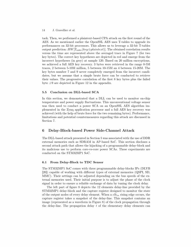
Fig. 7: DLL-based attack results: the bottom part represents the impact of anAES encryption on the DLL command value. The top part zooms on the AESencryption windows and provides the temporal correlation rate for two key bytes.
first experiment (in black), the victim program was kept idle during the entiretyof the DMA sampling operations. The DLL command drop visible between sam-ple 0 and 1,000 was induced by the extra power consumption linked to the DMAmodule activation. The DLL applied a strong correction to maintain a constantphase shift, that was finally relaxed as the power consumption returned to nor-mal (sample 2,000 to the end of sampling). The second case (in red) reportsan actual iteration of the attack and victim processes when an AES encryptionis done. The red trace experienced the same DLL command undershoot dueto DMA module activation (sample 0 to 1,000) but also a second undershootcorresponding to the AES encryption (starting at sample 4,500). It is finallyrestored to a steady value lower than the initial one (sample 6,000 to the end ofsampling). The AES encryption window was deduced from the position of thesecond DLL command drop. Based on this information the CPA attack couldbe conducted on a smaller amount of samples.
We launched a total number of 20 million AES encryptions and acquired200 DLL command samples per encryption. Samples and plaintexts extractionthrough UART took around 8 hours at 921,600 bauds. Then, an external com-puter was used to apply post-processing to the traces and conduct the CPAattack. The top part of Figure 7 depicts a filtered and averaged trace of the DLLcommand (in red). High-pass filtering was used as a way to reduce the impact oflow frequency variations (induced for instance by temperature fluctuations) onthe acquired traces and thus to reduce the number of traces required for the at-
14 J. Gravellier et al.
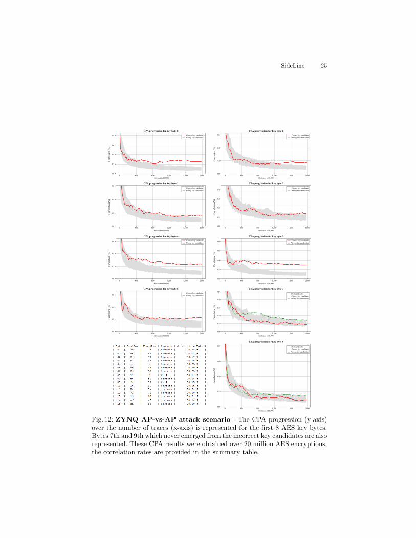
tack. Then, we performed a plaintext-based CPA attack on the first round of theAES. As we mentioned earlier the OpenSSL AES uses T-tables to upgrade itsperformances on 32-bit processors. This allows us to leverage a 32-bit T-tablesoutput prediction: HW [Ttable(key⊕plaintext)]. The obtained correlation resultsversus the time are represented above the averaged trace in Figure 7 (for twokey bytes). The correct key hypotheses are depicted in red and emerge from theincorrect hypotheses (in grey) at sample 120. Based on 20 million encryptions,we achieved a full AES key recovery. 3 bytes were retrieved in the range 0-5Mtraces, 2 between 5-10M million, 5 between 10-15M an 4 between 15-20M. Thekey bytes number 7 and 9 never completely emerged from the incorrect candi-dates, but we assume that a simple brute force can be conducted to retrievetheir values. The progressive correlation of the first 8 key bytes plus the failedbyte #9 are depicted in Figure 12 in the appendix.
5.5 Conclusion on DLL-based SCA
In this section, we demonstrated that a DLL can be used to monitor on-chiptemperature and power supply fluctuations. This unconventional voltage sensorwas then used to conduct a power SCA on an OpenSSL AES algorithm im-plemented in the Zynq application processor and a full AES key recovery wasachieved (with the help of brute force for the two remaining bytes). Performance,limitations and potential countermeasures regarding this attack are discussed inSection 7.
6 Delay-Block-based Power Side-Channel Attack
The DLL-based attack presented in Section 5 was associated with the use of DDRexternal memories such as SDRAM in AP-based SoC. This section discloses asecond attack path that allows the hijacking of a programmable delay-block andits malicious use to perform core-vs-core power SCAs. These experiments areconducted on the STM32MP1 SoC.
6.1 From Delay-Block to TDC Sensor
The STM32MP1 SoC comes with three programmable delay-blocks IPs (DLYB[20]) capable of working with different types of external memories (QSPI, SD,MMC). Their settings can be adjusted depending on the bus speeds of the ex-ternal memories used. Their initial purpose is to adjust the phase of the clocksignal in order to ensure a reliable exchange of data by tuning the clock delay.
The left part of figure 8 depicts the 12 elements delay-line provided by theSTM32MP1 delay-block and the capture register designed to monitor the stateof the output nodes of every delay element. When a clkin rising edge occurs, thecapture register takes a snapshot of the delay-line. This snapshot contains animage (represented as a waveform in Figure 8) of the clock propagation throughthe delay-line. The propagation delay t of the elementary delay elements can

SideLine 15
Fig. 8: Effect of on-chip voltage variations on the sampled delay values.
be set using a dedicated register. If this delay is set to its minimum the delay-line width (acquisition window) is small. Thus, only a part of the clock signalcan be captured. By gradually increasing t, the clock signal observation can beextended, possibly to several periods.
We leveraged this t parameter to make the delay-block sensitive to on-chipvoltage fluctuations. To that end, we took a significant number of delay-line snap-shots for each of the 128 possible t delay values. A vast majority of them gavestable results; which means that the captured image remained stable betweensuccessive register readings. For a few however, delay variations arose betweensubsequent captures. This interesting behavior can be explained by (1) on-chipvoltage fluctuations that affect the clock propagation time through the delayelements, and (2) by the fact that several delay values t naturally position theclock edges in unstable places within the delay line (i.e. in between two delay ele-ments). The left part of figure 8 displays three waveforms (delay-line snapshots)obtained with such a t setting. In this configuration, three clock periods stand inthe entire delay line. From top to bottom we have: (1) the steady state registerwaveform which stands as our reference (it outputs a 0x666 reference value), (2)a slowed down waveform that can be obtained due to a supply voltage decrease(it outputs a 0x64c), and (3) an accelerated waveform that can be obtained dueto a supply voltage increase (it outputs a 0x262). In our experiments, the threeobtained hexadecimal digits are weighted and added to translate into an imageof the voltage supply.
On the right part of figure 8, a program displays as an oscilloscope the actualdelay-line state on the STM32MP1 touchscreen. This way, the actual power con-sumption noise impact on the delay-block state can be directly observed. To makeit possible, the implemented program automatically calibrates the delay-blockby testing various delay parameters. For each delay value, it collects multipledelay-line state samples, computes their variance and adopts the calibration thatprovided the highest variance. Indeed, a higher variance indicates an importantdelay instability and thus a stronger relationship with voltage fluctuations.
6.2 Linux-based OpenSSL AES Attack Setup
Similarly to the attack setup described in subsection 5.3, we used the OpenSSLAES implementation to evaluate the threat posed by delay-block-based SCAs.
16 J. Gravellier et al.
The STM32MP1 embeds both a dual core AP and a MCU that makes it possibleto test the MCU-vs-AP and AP-vs-MCU attack scenarios introduced in subsec-tion 4.3. Depending on the scenario, the attack and victim processes were raneither on the AP core or on the MCU core. Here, we consider the MCU-vs-APattack to describe our attack setup.
We use an adapted version of the Zynq-based attack. On the adversary’sside (here the MCU), delay-block calibration and use of Hardware PerformanceCounters (HPCs) were added to the initial algorithm. HPCs are used to accu-rately time the successive encryptions and to mitigate the de-synchronisationbrought by the Linux OS. For each acquisition, the number of cycles elapsedduring the encryption is compared to a maximal limit Nbcycle set by the ad-versary above which the entire acquisition is discarded. Prior to the attack, apreliminary test was conducted in order to identify the optimal value for Nbcycle(assuming that a lower number of clock cycles corresponds to a lower numberof interrupts). Hence, by launching thousands of AES encryptions, we were ableto find a reference number of clock cycles for almost interrupt-free encryptions.Then, based on this reference, we set a maximal limit Nbcycle beyond whichwe decided to discard the acquisitions. By doing so, at least half of the totalacquisitions were retained and used for the subsequent CPA calculations.
Regarding the CPA, we embedded it directly within the STM32MP1. Thisway, we drastically limited the amount of data exported. Moreover, this allowedus to directly plot the results on screen as illustrated in appendix figure 11.
6.3 Delay-block-based SCA Attacks on STM32MP1 SoC
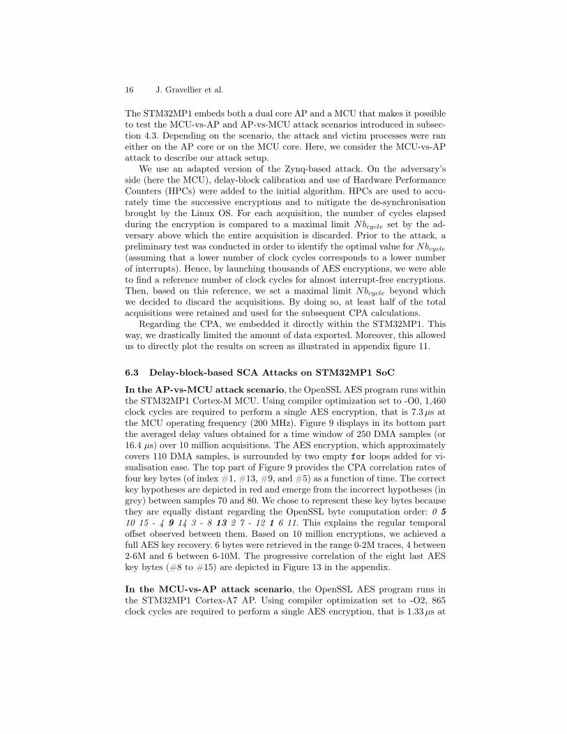
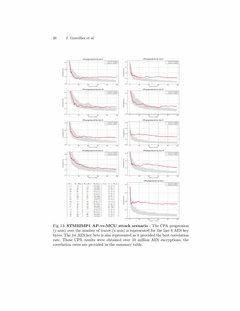
In the AP-vs-MCU attack scenario, the OpenSSL AES program runs withinthe STM32MP1 Cortex-M MCU. Using compiler optimization set to -O0, 1,460clock cycles are required to perform a single AES encryption, that is 7.3µs atthe MCU operating frequency (200 MHz). Figure 9 displays in its bottom partthe averaged delay values obtained for a time window of 250 DMA samples (or16.4 µs) over 10 million acquisitions. The AES encryption, which approximatelycovers 110 DMA samples, is surrounded by two empty for loops added for vi-sualisation ease. The top part of Figure 9 provides the CPA correlation rates offour key bytes (of index #1, #13, #9, and #5) as a function of time. The correctkey hypotheses are depicted in red and emerge from the incorrect hypotheses (ingrey) between samples 70 and 80. We chose to represent these key bytes becausethey are equally distant regarding the OpenSSL byte computation order: 0 510 15 - 4 9 14 3 - 8 13 2 7 - 12 1 6 11. This explains the regular temporaloffset observed between them. Based on 10 million encryptions, we achieved afull AES key recovery. 6 bytes were retrieved in the range 0-2M traces, 4 between2-6M and 6 between 6-10M. The progressive correlation of the eight last AESkey bytes (#8 to #15) are depicted in Figure 13 in the appendix.
In the MCU-vs-AP attack scenario, the OpenSSL AES program runs inthe STM32MP1 Cortex-A7 AP. Using compiler optimization set to -O2, 865clock cycles are required to perform a single AES encryption, that is 1.33µs at

SideLine 17
Fig. 9: AP-vs-MCU attack results: the bottom part represents the averaged AESpower consumption, the top part provides the correlation rates as a function oftime for four AES key bytes.
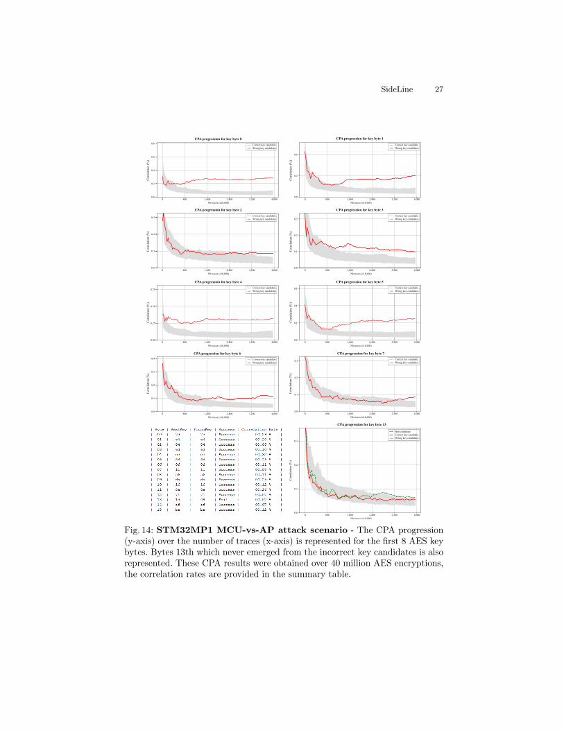
the AP operating frequency (650 MHz). Figure 10 displays in its bottom partthe averaged delay value obtained for a time window of 100 DMA samples (or6,6 µs) over 40 million acquisitions. The AES encryption, which approximatelycovers 20 DMA samples, is surrounded by two empty for loops added for visu-alisation ease. The top part of Figure 10 provides the temporal correlation rateof four key bytes as a function of time . The correct key hypotheses are depictedin red and emerge from the incorrect hypotheses (in grey) between samples 30and 40. Again, we chose to represent these specific key bytes because they areequally distant in the OpenSSL byte computation order. However, the AES en-cryption in the AP is faster than that of the MCU (1.33 µs vs. 7.3 µs) and theDMA sampling frequency that remained fixed between the two experiments isno longer sufficient to let the temporal offsets appear. This limited samplingfrequency partly explains the higher number of acquisitions required to retrievesome key bytes. For instance, byte #12 in Figure 10, seems to suffer from the un-der sampling and gave poorer correlation results (0,07%) than byte #4 (0,32%)or byte #0 (0,29%). We were able to confirm this assumption through a sec-ond experiment where the AES encryption temporal window had been slightlyshifted regarding the DMA: the AES leakage was thus sampled at different tim-ings. This experiment gave better results on several key bytes that struggled toemerge in the previous attack. Based on 40 million encryptions, we achieved afull AES key recovery. 3 bytes were retrieved in the range 0-10M traces, 6 be-tween 10-20M, 2 between 40-30M, 4 between 30-40M. The 13th key byte nevercompletely emerged from the incorrect candidates, but we assume that a simplebrute force can be conducted to retrieve its value. The progressive correlation ofthe first key bytes (0 to 7) are depicted in Figure 14 in the appendix.

18 J. Gravellier et al.
Fig. 10: MCU-vs-AP attack results: the bottom part represents the averagedAES power consumption. The top part provides the correlation over the timeresults over four AES key bytes.
7 Discussion
Two delay-line-based power measurement techniques, using a DLL or a delay-block were introduced and studied in this research work. Because such delay-line-based components are embedded in almost every high-end digital SoC thatuses external memories, the threat model we introduced is serious and shallbe considered feasible for a large number of complex SoCs. In this section, wediscuss performance, additional attack scenarios and potential countermeasuresregarding the SideLine attack.
7.1 Performance and Limitations of SideLine
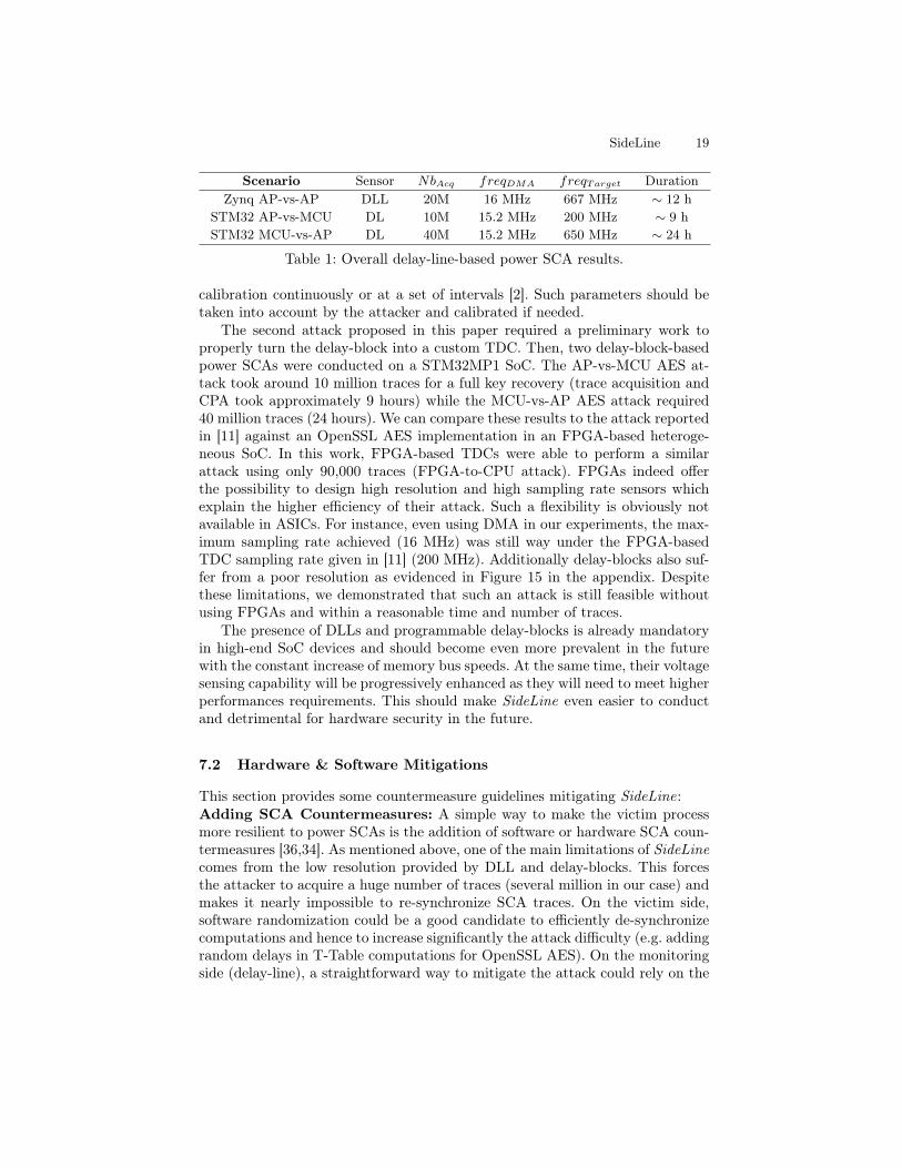
Table 1 summarizes the results obtained for the three attack scenarios consid-ered in this paper. First, an AP-vs-AP attack was performed on a Zynq SoCusing DLL-based sensors. As DLLs provide a limited resolution, a large amountof acquisitions were required to integrate enough information for the CPA tosucceed (20 million traces required for full AES key recovery). It took around12 hours to extract the traces, apply post-processing (filtering) and conductthe CPA attack. The lack of resolution also made post-synchronization nearlyimpossible and thus implied the collection of leakage traces with a constant syn-chronization. Apart from performances, the DLL was by far the simplest sensorto implement in our experiments, as it only required the reading of a memory-mapped register. However, care must be taken as in certain cases, DLLs mayrequire additional calibration. For instance, some DLLs can either perform delay
SideLine 19
Scenario Sensor NbAcq freqDMA freqTarget DurationZynq AP-vs-AP DLL 20M 16 MHz 667 MHz ∼ 12 h
STM32 AP-vs-MCU DL 10M 15.2 MHz 200 MHz ∼ 9 hSTM32 MCU-vs-AP DL 40M 15.2 MHz 650 MHz ∼ 24 h
Table 1: Overall delay-line-based power SCA results.
calibration continuously or at a set of intervals [2]. Such parameters should betaken into account by the attacker and calibrated if needed.
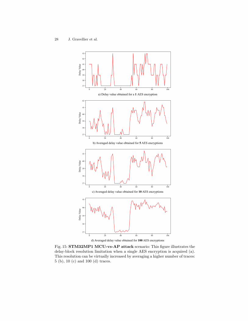
The second attack proposed in this paper required a preliminary work toproperly turn the delay-block into a custom TDC. Then, two delay-block-basedpower SCAs were conducted on a STM32MP1 SoC. The AP-vs-MCU AES at-tack took around 10 million traces for a full key recovery (trace acquisition andCPA took approximately 9 hours) while the MCU-vs-AP AES attack required40 million traces (24 hours). We can compare these results to the attack reportedin [11] against an OpenSSL AES implementation in an FPGA-based heteroge-neous SoC. In this work, FPGA-based TDCs were able to perform a similarattack using only 90,000 traces (FPGA-to-CPU attack). FPGAs indeed offerthe possibility to design high resolution and high sampling rate sensors whichexplain the higher efficiency of their attack. Such a flexibility is obviously notavailable in ASICs. For instance, even using DMA in our experiments, the max-imum sampling rate achieved (16 MHz) was still way under the FPGA-basedTDC sampling rate given in [11] (200 MHz). Additionally delay-blocks also suf-fer from a poor resolution as evidenced in Figure 15 in the appendix. Despitethese limitations, we demonstrated that such an attack is still feasible withoutusing FPGAs and within a reasonable time and number of traces.
The presence of DLLs and programmable delay-blocks is already mandatoryin high-end SoC devices and should become even more prevalent in the futurewith the constant increase of memory bus speeds. At the same time, their voltagesensing capability will be progressively enhanced as they will need to meet higherperformances requirements. This should make SideLine even easier to conductand detrimental for hardware security in the future.
7.2 Hardware & Software Mitigations
This section provides some countermeasure guidelines mitigating SideLine:Adding SCA Countermeasures: A simple way to make the victim processmore resilient to power SCAs is the addition of software or hardware SCA coun-termeasures [36,34]. As mentioned above, one of the main limitations of SideLinecomes from the low resolution provided by DLL and delay-blocks. This forcesthe attacker to acquire a huge number of traces (several million in our case) andmakes it nearly impossible to re-synchronize SCA traces. On the victim side,software randomization could be a good candidate to efficiently de-synchronizecomputations and hence to increase significantly the attack difficulty (e.g. addingrandom delays in T-Table computations for OpenSSL AES). On the monitoringside (delay-line), a straightforward way to mitigate the attack could rely on the

20 J. Gravellier et al.
addition of phase and frequency jitter to the clock signal used for sampling thedelay-line registers.Preventing Delay-Line Access: Another countermeasure would act at systemlevel by preventing the access to the delay-line registers by unauthorized softwareentities. Hence, only the OS for instance would have access to this resource.TrustZone could also be used to place DLLs and Delay-blocks in the secureworld and make their use by non-secure world impossible in practice. Lockingthe access to the DMA module or the hardware performance counters would alsorepresent a significant limitation for the attack setup.Reducing Delay-Line Sampling Rate: Preventing delay-line access throughprivilege rights seems insufficient as a malicious attacker or a compromised OScould overpass it (privileges escalation). A hardware way to mitigate the threatwould be to limit the delay-block access to a lower sampling rate (e.g. 10KHz).This could be simply achieved by limiting the access rate to the register thatstores delay-line information. This way, even if the power consumption monitor-ing would remain feasible, it will highly affect the delay sensor performances.With such a limited sampling rate it would be probably very challenging for anattacker to conduct SCAs on fast encryption algorithms such as AES.Abandoning Delay-Lines in SoCs: As SideLine revealed their potential mis-use as power consumption sensors, the delay-line-based components could beremoved from SoC devices and instead, be placed directly within the externalmemory devices. This drastic choice would require the addition of configurationI/Os in external memories to efficiently calibrate the delay-lines but will almostentirely remove the delay-line threat from the SoC die. However, even outsidethe SoC, the delay-line threat may remain problematic as inter-chip power SCAshave already been shown feasible [27].
8 Conclusion
Previous works demonstrated that remote power SCAs were feasible using FPGA-based delay sensors and microcontroller ADC-based sensors. SideLine goes fur-ther by proving that unsuspected hardware components available in a broadrange of high-end SoC devices, can be turned into power consumption mea-surement units. In this work, we studied two common SoC resources knownas delay-locked-loops and delay-blocks and proved their capability to eavesdropthe voltage activity of cryptographic programs running in different processors.Several core-vs-core attack scenarios on application processors and microcon-troller units were conducted. For each scenario, we achieved a full key recoveryside-channel attack on the publicly available OpenSSL AES implementation. Webelieve that these findings open a new era for remote power side-channel attacks.SideLine has the advantage of being portable on a wide range of devices as itdoes not requires the presence of specific circuitry (e.g. FPGA). Because Side-Line feeds upon SoC complexity, we also believe that it represents a major threatfor actual high-end SoC security. More importantly this threat is likely to scaleup in line with the constant performance improvements in SoCs and memorydevices.
SideLine 21
References
1. Bilal I Abdulrazzaq, Izhal Abdul Halin, Shoji Kawahito, Roslina M Sidek, SuhaidiShafie, and Nurul Amziah Md. Yunus. A review on high-resolution CMOS delaylines towards sub-picosecond jitter performance. SpringerPlus, 2016.
2. Limited ARM. ARM PrimeCell MultiPort Memory Controller (PL176) TechnicalReference Manual. Technical report, 2003.
3. Eric Brier, Christophe Clavier, and Francis Olivier. Correlation Power Analysiswith a Leakage Model. Cryptographic Hardware and Embedded Systems, 2004.
4. Sebanjila Kevin Bukasa, Ronan Lashermes, Hélène Le Bouder, Jean-Louis Lanet,and Axel Legay. How TrustZone Could Be Bypassed: Side-Channel Attacks on aModern System-on-Chip. In Lecture Notes in Computer Science. 2018.
5. Claudio Canella, Daniel Genkin, Lukas Giner, Daniel Gruss, Moritz Lipp, MarinaMinkin, Daniel Moghimi, Frank Piessens, Michael Schwarz, Berk Sunar, Jo VanBulck, and Yuval Yarom. Fallout: Leaking data on meltdown-resistant CPUs.Proceedings of the ACM Conference on Computer and Communications Security,2019.
6. Fei Chen, Yi Shan, Yu Zhang, Yu Wang, Hubertus Franke, Xiaotao Chang, andKun Wang. Enabling FPGAs in the cloud. In ACM Computing Frontiers, 2014.
7. Ching Che Chung, Pao Lung Chen, and Chen Yi Lee. An all-digital delay-lockedloop for DDR SDRAM controller applications. In International Symposium onVLSI Design, Automation and Test, 2007.
8. Joan Daemen and Vincent Rijmen. The Rijndael Block Cipher. 1999.9. Jean-Max Dutertre, Bruno Robisson, Assia Tria, and Loic Zussa. Investigation
of timing constraints violation as a fault injection means. Design of Circuits andIntegrated Systems, 2012.
10. Dennis R. E. Gnad, Jonas Krautter, and Mehdi B. Tahoori. Leaky Noise : NewSide-Channel Attack Vectors in Mixed-Signal IoT Devices. IACR Transactions onCryptographic Hardware and Embedded Systems, 2019.
11. Joseph Gravellier, Jean-max Dutertre, Philippe Loubet Moundi, Yannick Teglia,and Francis Olivier. Remote Side-Channel Attacks on Heterogeneous SoC. 18thSmart Card Research and Advanced Application Conference, 2019.
12. Daniel Gruss, Clémentine Maurice, and Stefan Mangard. Rowhammer.js: A Re-mote Software-Induced Fault Attack in JavaScript. Detection of Intrusions andMalware, and Vulnerability Assessment, jul 2015.
13. Zijo Kenjar, Tommaso Frassetto, David Gens, Michael Franz, and Ahmad-RezaSadeghi. V0LTpwn: Attacking x86 Processor Integrity from Software. CoRR,2019.
14. Yoongu Kim, Ross Daly, Jeremie Kim, Chris Fallin, Ji Hye Lee, Donghyuk Lee,Chris Wilkerson, Konrad Lai, and Onur Mutlu. Flipping bits in memory withoutaccessing them: An experimental study of DRAM disturbance errors. In 2014ACM/IEEE 41st International Symposium on Computer Architecture (ISCA),pages 361–372, jun 2014.
15. Paul Kocher, Jann Horn, Anders Fogh, Daniel Genkin, Daniel Gruss, Werner Haas,Mike Hamburg, Moritz Lipp, Stefan Mangard, Thomas Prescher, Michael Schwarz,and Yuval Yarom. Spectre Attacks: Exploiting Speculative Execution. In 2019IEEE Symposium on Security and Privacy (SP), may 2019.
16. Paul Kocher, Joshua Jaffe, and Benjamin Jun. Differential Power Analysis. Ad-vances in Cryptology, 1999.
22 J. Gravellier et al.
17. Anil Kurmus, Nikolas Ioannou, Matthias Neugschwandtner, Nikolaos Papandreou,and Thomas Parnell. From random block corruption to privilege escalation: Afilesystem attack vector for rowhammer-like attacks. 11th USENIX Workshop onOffensive Technologies, 2017.
18. Moritz Lipp, Andreas Kogler, David Oswald, Michael Schwarz, Catherine Eas-don, Claudio Canella, and Daniel Gruss. PLATYPUS: Software-based Power Side-Channel Attacks on x86. In 2021 IEEE Symposium on Security and Privacy (SP).IEEE, 2021.
19. Moritz Lipp, Michael Schwarz, Daniel Gruss, Thomas Prescher, Werner Haas, Ste-fan Mangard, Paul Kocher, Daniel Genkin, Yuval Yarom, and Mike Hamburg.Meltdown. CoRR, jan 2018.
20. ST Microelectronics. STM32MP1 Reference manual. 2019.21. K Murdock, D Oswald, F D Garcia, J Van Bulck, D Gruss, and Frank Piessens.
Plundervolt: Software-based Fault Injection Attacks against Intel SGX. 41st IEEESymposium on Security and Privacy, 2020.
22. Colin O’Flynn and Alex Dewar. On-Device Power Analysis Across Hardware Secu-rity Domains.: Stop Hitting Yourself. IACR Transactions on Cryptographic Hard-ware and Embedded Systems, 2019.
23. OpenSSL Software Foundation. https://www.openssl.org/, 2002.24. Pengfei Qiu, Dongsheng Wang, Yongqiang Lyu, and Gang Qu. Voltjockey: Breach-
ing trustzone by software-controlled voltage manipulation over multi-core frequen-cies. Proceedings of the ACM Conference on Computer and Communications Se-curity, 2019.
25. Joaquin Romo. DDR Memories Comparison and overview.26. Falk Schellenberg, Dennis R. E. Gnad, Amir Moradi, and Mehdi B. Tahoori. An
inside job: Remote power analysis attacks on FPGAs. In Design, Automation &Test in Europe Conference & Exhibition, 2018.
27. Falk Schellenberg, Dennis R. E. Gnad, Amir Moradi, and Mehdi B. Tahoori. Re-mote inter-chip power analysis side-channel attacks at board-level. In Proceedingsof the International Conference on Computer-Aided Design, New York, NY, USA,nov 2018. ACM.
28. Adrian Tang, Simha Sethumadhavan, and Salvatore Stolfo. CLKSCREW: Expos-ing the Perils of Security-Oblivious Energy Management. In 26th USENIX SecuritySymposium (USENIX Security 17), 2017.
29. Jo Van Bulck, Marina Minkin, Ofir Weisse, Daniel Genkin, Baris Kasikci, FrankPiessens, Mark Silberstein, Thomas F Wenisch, Yuval Yarom, and Raoul Strackx.Foreshadow: Extracting the Keys to the Intel SGX Kingdom with Transient out-of-Order Execution. In Proceedings of the 27th USENIX Conference on SecuritySymposium, SEC’18, USA, 2018. USENIX Association.
30. S van Schaik, A Milburn, S Österlund, P Frigo, G Maisuradze, K Razavi, H Bos,and C Giuffrida. RIDL: Rogue In-Flight Data Load. In 2019 IEEE Symposium onSecurity and Privacy (SP), 2019.
31. Colin D Walter. Simple Power Analysis of Unified Code for ECC Double and Add.In Cryptographic Hardware and Embedded Systems, 2004.
32. Zane Weissman, Thore Tiemann, Daniel Moghimi, Evan Custodio, Thomas Eisen-barth, and Berk Sunar. JackHammer: Efficient Rowhammer on HeterogeneousFPGA-CPU Platforms. IACR Transactions on Cryptographic Hardware and Em-bedded Systems, dec 2020.
33. Xilinx. Zynq-7000 SoC Data Sheet. 190:1–25, 2012.34. Lu Zhang, Luis Vega Gutierrez, and Michael Bedford Taylor. Power Side Channels
in Security ICs: Hardware Countermeasures. CoRR, 2016.

SideLine 23
35. Mark Zhao and G. Edward Suh. FPGA-Based Remote Power Side-Channel At-tacks. In IEEE Symposium on Security and Privacy, 2018.
36. Yongbin Zhou and DengGuo Feng. Side-Channel Attacks: Ten Years After ItsPublication and the Impacts on Cryptographic Module Security Testing. IACRCryptology ePrint Archive, 2005.
37. Kenneth M. Zick and John P. Hayes. Low-cost sensing with ring oscillator arrays forhealthier reconfigurable systems. ACM Transactions on Reconfigurable Technologyand Systems, 2012.
38. Kenneth M. Zick, Meeta Srivastav, Wei Zhang, and Matthew French. Sensingnanosecond-scale voltage attacks and natural transients in FPGAs. ACM/SIGDA,2013.

24 J. Gravellier et al.
9 Appendix
Algorithm 1 Zynq processor attack, AP#0 attack pseudo-algorithmInput: Nbacq, Nbsample
DMAinit();UARTinit();while Nbacq has not been reached do
Send AES plaintext to AP#1;Launch DMA transfer(Nbsample);Send StartAES to AP#1;Wait for EndAES flag();Wait for EndDMA flag();Export samples through UART;
end while
Algorithm 2 Zynq processor attack, AP#1 victim pseudo-algorithmInput: AESkey, AESplaintext
AESinit();while infinity do
Wait for StartAES flag();Get AP#0 plaintext;OpenSSL AES encrypt();Send EndAES flag to AP#0;Send AES ciphertext to AP#0;
end while
Fig. 11: AES traces acquisition, CPA computation and GTK display (imple-mented for demonstration) are all embedded in the same application runningwithin the STM32MP157-DK2 board.
SideLine 25
Fig. 12: ZYNQ AP-vs-AP attack scenario - The CPA progression (y-axis)over the number of traces (x-axis) is represented for the first 8 AES key bytes.Bytes 7th and 9th which never emerged from the incorrect key candidates are alsorepresented. These CPA results were obtained over 20 million AES encryptions,the correlation rates are provided in the summary table.
26 J. Gravellier et al.
Fig. 13: STM32MP1 AP-vs-MCU attack scenario - The CPA progression(y-axis) over the number of traces (x-axis) is represented for the last 8 AES keybytes. The 1st AES key byte is also represented as it provided the best correlationrate. These CPA results were obtained over 10 million AES encryptions, thecorrelation rates are provided in the summary table.
SideLine 27
Fig. 14: STM32MP1 MCU-vs-AP attack scenario - The CPA progression(y-axis) over the number of traces (x-axis) is represented for the first 8 AES keybytes. Bytes 13th which never emerged from the incorrect key candidates is alsorepresented. These CPA results were obtained over 40 million AES encryptions,the correlation rates are provided in the summary table.
28 J. Gravellier et al.
Fig. 15: STM32MP1 MCU-vs-AP attack scenario: This figure illustrates thedelay-block resolution limitation when a single AES encryption is acquired (a).This resolution can be virtually increased by averaging a higher number of traces:5 (b), 10 (c) and 100 (d) traces.