shape-controlled deterministic assembly of nanowires€¦ · · 2016-03-25shape-controlled...
TRANSCRIPT

Shape-Controlled Deterministic Assembly of NanowiresYunlong Zhao,† Jun Yao,† Lin Xu,†,§ Max N. Mankin,† Yinbo Zhu,⊥ Hengan Wu,⊥ Liqiang Mai,§
Qingjie Zhang,§ and Charles M. Lieber*,†,‡
†Department of Chemistry and Chemical Biology and ‡Harvard John A. Paulson School of Engineering and Applied Sciences,Harvard University, Cambridge, Massachusetts 02138, United States§State Key Laboratory of Advanced Technology for Materials Synthesis and Processing, Wuhan University of Technology, Wuhan430070, China⊥CAS Key Laboratory of Mechanical Behavior and Design of Materials, Department of Modern Mechanics, University of Science andTechnology of China, Hefei, Anhui 230027, China
*S Supporting Information
ABSTRACT: Large-scale, deterministic assembly of nano-wires and nanotubes with rationally controlled geometriescould expand the potential applications of one-dimensionalnanomaterials in bottom-up integrated nanodevice arrays andcircuits. Control of the positions of straight nanowires andnanotubes has been achieved using several assembly methods,although simultaneous control of position and geometry hasnot been realized. Here, we demonstrate a new conceptcombining simultaneous assembly and guided shaping toachieve large-scale, high-precision shape controlled deterministic assembly of nanowires. We lithographically pattern U-shapedtrenches and then shear transfer nanowires to the patterned substrate wafers, where the trenches serve to define the positions andshapes of transferred nanowires. Studies using semicircular trenches defined by electron-beam lithography yielded U-shapednanowires with radii of curvature defined by inner surface of the trenches. Wafer-scale deterministic assembly produced U-shapednanowires for >430 000 sites with a yield of ∼90%. In addition, mechanistic studies and simulations demonstrate that shapingresults in primarily elastic deformation of the nanowires and show clearly the diameter-dependent limits achievable for accessibleforces. Last, this approach was used to assemble U-shaped three-dimensional nanowire field-effect transistor bioprobe arrayscontaining 200 individually addressable nanodevices. By combining the strengths of wafer-scale top-down fabrication with diverseand tunable properties of one-dimensional building blocks in novel structural configurations, shape-controlled deterministicnanowire assembly is expected to enable new applications in many areas including nanobioelectronics and nanophotonics.
KEYWORDS: Silicon nanowires, nanowire arrays, elastic deformation, bioelectronics, nanoelectronics, field-effect transistors
Interest in the assembly of nanoscale wires, such assemiconductor nanowires and carbon nanotubes, has long
been motivated by the development of bottom-up integratednanodevice arrays and circuits.1−6 Existing assembly methods7,8
have been used to align9−17 and in some cases deterministicallyposition18−22 straight nanoscale wires. These methods haveused a variety of forces to achieve alignment includingmechanical,9,18,22 electric,19,20 magnetic,7 liquid surface ten-sion,10,12,15 optical,13,17 and chemical.14,16,21 In addition,patterning regions of selective interaction on substrates havealso been used with some success for deterministicassembly.18−22 Most recently, we have described a nano-combing assembly method18,22 that allowed for separateanchoring and then straightening/aligning of nanowires withshear forces and showed that this could be used to assemble bydeterministic design large-scale integrated finite state ma-chine.22
These latter studies, which separate anchoring from align-ment, suggest that the flexibility and large elastic strainssustainable in nanoscale wires23,24 could be exploited with the
combing method to assemble nanoscale wires with well-controlled curvature. Assembly of nanoscale wires with definedcurvature and position could open up many opportunities notpossible with straight nanoscale wires and thus represents animportant target. Conceptually, to realize shape control duringdeterministic assembly requires that (i) applied forces aresufficiently large to bend the nanoscale wires, and (ii) thebending curvature and directions should be rationallycontrolled at the nanoscale. Here we address these require-ments by introducing controlled curvature anchors to enableguided shaping during nanowire combing.Our assembly method (Figure 1a) involves two key steps.
First, trenches with designed shapes are patterned in a surfacelayer on the target substrate (Figure 1a(i)). Second, thenanowire growth substrate is flipped over and translated with afixed normal load and specific orientation with respect to the
Received: January 22, 2016Revised: March 15, 2016
Letter
pubs.acs.org/NanoLett
© XXXX American Chemical Society A DOI: 10.1021/acs.nanolett.6b00292Nano Lett. XXXX, XXX, XXX−XXX

trenches over the target substrate.18 During this latter process(Figure 1a(ii)), the trench structures serve to anchor and guidethe bending of nanowires during the shear transfer process withoverall alignment determined by the linear translation.A prototypical example of our concept is shape-controlled
deterministic assembly of U-shaped nanowires as it captures allof the essential elements of the assembly process; that is, the U-shape structure requires assembly to define the radius ofcurvature, position, and alignment. We first explored thecapabilities of our approach in wafer scale deterministicassembly. First, photolithography was used to define>430 000 U-shaped trenches in nine arrays on a 3 in. wafer,where the trench radius of curvature and depth were 1.5 μmand 260 nm, respectively (see Materials and Methods inSupporting Information). This patterned target substrate wasmounted on a linear translation stage, coated with highviscosity mineral oil, and then the nanowire growth substrate(randomly distributed and straight silicon nanowires: lengths,40−80 μm; mean diameter, 80 nm) was placed on the targetsubstrate. After the pressure was set between the patternedtarget and nanowire growth substrates (∼4.8 N cm−2 in thisexperiment), the target substrate was translated in a directionperpendicular to the tangent of the U-shape (red arrow, Figure1b) at a constant velocity.
Optical microscopy and scanning electron microscopy(SEM) images of the assembled nanowire arrays (Figure1b,c) show several important features. First, U-shaped nano-wires are uniformly assembled on the patterned regions of thewhole wafer with pitch of adjacent nanowires of 15 μm androw-to-row pitch of 100 μm. The overall assembly yield, whichis estimated from statistics from several different areas, eachfeaturing a size of 1.5 × 1.5 mm2 and containing 1500 sites(trench depth, 260 nm), is 86−94%. Specifically, 43−51% ofthe trenches contain a single nanowire. Second, nanowires areprecisely anchored in the U-shaped trenches. The nanowireradii of curvature in these experiments are defined by the inneredge of the trenches, and thus it is not necessary to definenanometer width trenches to match the nanowire diameters toachieve precise assembly.We assembled nanowires in U-shaped trenches with varying
width and depth to determine how these parameters affectassembly yield (Figure S1). First, the overall yield increaseswith trench width, with >90% for widths ≥ 2 μm. Second, weobserved that when trench depth is less than the nanowirediameter, the anchoring yield is close to zero, but the yieldincreases to >90% for depths ≥ ∼4-times the nanowirediameter. We fabricated U-shaped trenches with different radiiof curvature to rationally control the radii of curvature ofnanowires. SEM images of 80 nm diameter nanowires
Figure 1. Shape-controlled nanowire assembly. (a) Schematic of deterministic assembly of U-shaped nanowire arrays. The red arrow (right side)shows the sliding direction of the nanowire growth substrate with respect to the target substrate. (b) Photograph and optical images of wafer-scaledeterministically assembled U-shaped silicon nanowire arrays by trenches. Nanowire diameter is 80 nm. The arrow in (i) shows the sliding directionof the nanowire growth substrate with respect to the target substrate. Scale bars in (i)−(iii) are 10 mm, 200 μm, and 50 μm, respectively. (c)Representative SEM image of U-shaped silicon nanowire array. Scale bar, 20 μm. (d) Plot of the radius of nanowire curvature versus the trenchradius of curvature. Nanowire diameter is 80 nm. Insets: Representative SEM images of U-shaped silicon nanowires assembled by U-shaped trencheswith controlled radius, R, of curvature: (i) 1 μm; (ii) 2 μm; (iii) 3 μm. Nanowire diameter is 80 nm. Scale bars, 2 μm.
Nano Letters Letter
DOI: 10.1021/acs.nanolett.6b00292Nano Lett. XXXX, XXX, XXX−XXX
B

assembled in trenches with radii of curvature from 1−3 μm(Figure 1d) show that the nanowire curvature closely followsthe inner edge of trenches for these different radii; we addresslower limits versus nanowire diameter further.We conducted experiments and modeling to understand
better the process and bending limits of shape-controlledassembly. First, we used a micromanipulator (SupportingInformation) to translate the growth substrate a short about100−200 μm distance over the target substrate trenches (vsacross the entire target substrate) to yield a distribution ofassembled nanowire positions from early to end stages ofassembly. Representative dark field optical microscopy images(Figure 2a) reveal that the roughly straight nanowires areinitially anchored on the inner edge of U-shaped trenches(Figure 2a(i)), then bend around the curved edge of thetrenches (Figure 2a(ii,iii)), and finally the two arms of nanowire
are aligned along the translation direction (Figure 2a(iv)). Onthe basis of these results and the trench width/depth dependentdata (Figure S1), we suggest that shape-controlled nanowireassembly (Figure 2b) proceeds by an anchor-bend-alignprocess. The trenches serve to initially anchor/mechanicallytrap nanowires, and then the shear force produced during thetransfer3,9,18,22 bends the nanowires around the shaped trenchand aligns their arms to the transfer direction.Second, we studied the effect of contact pressure on
nanowire curvature by transferring 80 nm diameter nanowiresinto trenches with small ∼200 nm radii of curvature. SEMimages (Figure S2) and analyses (Figure 2c; N = 10) fornanowires assembled with contact pressures of 0.8, 4.8, and 7.2N cm−2 yield radii of 2.0 ± 0.3, 1.3 ± 0.2, and 0.7 ± 0.2 μm andestimated strains (Figure 2c, inset) of 1.9 ± 0.3, 3.3 ± 0.3, and5.8 ± 0.4%, respectively; these values correspond to the
Figure 2. Shape-controlled nanowire assembly. (a) Optical images of nanowires at different stages of assembly and bending process. The red arrowsshow the sliding direction of the nanowire growth substrate with respect to the target substrate. Scale bars, 3 μm. (b) Schematics of anchor-bend-align assembly process. The red arrows show the sliding direction of the nanowire growth substrate with respect to the target substrate. (c) Plot ofsilicon nanowire R versus contact pressure. Left inset: Model and force analysis of nanowire bending during assembly. Right inset: Plot of strain ofsilicon nanowires versus contact pressure. Nanowire diameters are 80 nm. (d) Simulation of the deformation of the nanowire under bending loads0−20 nN/μm. (e) The corresponding radius of curvature at the fixed end calculated from the simulation results in panel d. (f) Plot of minimum Rversus nanowire diameter under standard assembly conditions (pressure = 4.8 N cm−2). Inset: Plot of nanowire strain versus diameter.
Nano Letters Letter
DOI: 10.1021/acs.nanolett.6b00292Nano Lett. XXXX, XXX, XXX−XXX
C

maximum strain at the surface of nanowires. A geometricallynonlinear finite element model (Supporting Information) wasused to simulate the large deformation of the nanowire underuniform distributed in-plane force, Fload. The simulation results(Figure 2d,e) show that the radius of curvature decreases andstrain increases with increasing Fload applied to nanowires.These results are thus consistent with the experimental dataand our suggestion that increasing contact pressure duringtransfer yields increased Fload. Last, we characterized theminimum radius of curvature as a function of nanowirediameter for a fixed contact pressure of 4.8 N cm−2. A summaryof results for assembly of U-shaped nanowires with diameters of10, 30, and 80 nm (Figure 2f, N = 10) yields minimum radii ofcurvature 0.16 ± 0.04, 0.36 ± 0.1, and 1.29 ± 0.17 μm andestimated strains of 3.2 ± 0.5, 4.0 ± 0.8, and 3.2 ± 0.4%,respectively. The 80 and 30 nm diameter nanowires wereassembled on 200 nm radii of inner curvature trenches
fabricated by electron-beam lithography, while the 10 nmdiameter nanowires were assembled on 75 nm radii ofcurvature gold nanoparticles (Supporting Information; FigureS3). These results show that smaller diameter nanowiresachieve smaller radii of curvature for fixed contact pressure andthus are consistent with the anchor-bend-align assemblyprocess.We fabricated free-standing mesh structures with assembled
arrays of different radii of curvature U-shaped silicon nanowiresto enable substrate-free studies of the nanowires (SupportingInformation). The arms of the assembled nanowires were fixedbetween Au layers while the suspended U-shaped nanowire tipswere left exposed (Figure 3a), and the mesh structure wastransferred onto a copper transmission electron microscopy(TEM) grid (Figure 3b) for characterization. First, a focusedion beam (FIB) was used to cut one arm of suspended U-shaped nanowires (Supporting Information), and in situ SEM
Figure 3. Strain characterization of shape-controlled nanowires. (a) Schematics highlighting the structure of the free-standing U-shaped siliconnanowire arrays with arms embedded in Au mesh. (b) Dark-field optical image of U-shaped silicon nanowire array fixed and encapsulated in adouble-layer gold mesh network transferred to a copper TEM grid. Scale bar, 50 μm. (c) A time sequence of three SEM images showing the releaseprocess for a U-shaped silicon nanowire (R = 1.5 μm) after cutting by FIB. (right) TEM image of a nanowire following FIB cutting. Scale bars, 1 μm.(d) Normalized Raman spectra acquired on silicon nanowires: (i) straight/unbent nanowire; (ii−iv) U-shaped tip with R = 3.0, 1.5, and 0.8 μm,respectively; and (v) roughly straight nanowire following FIB cutting on arm remote from bend (R = 1.5 μm prior to cutting). (e) Plot of full widthat half-maximum (fwhm) of the first-order Raman scattering mode versus R of assembled U-shaped silicon nanowires.
Nano Letters Letter
DOI: 10.1021/acs.nanolett.6b00292Nano Lett. XXXX, XXX, XXX−XXX
D

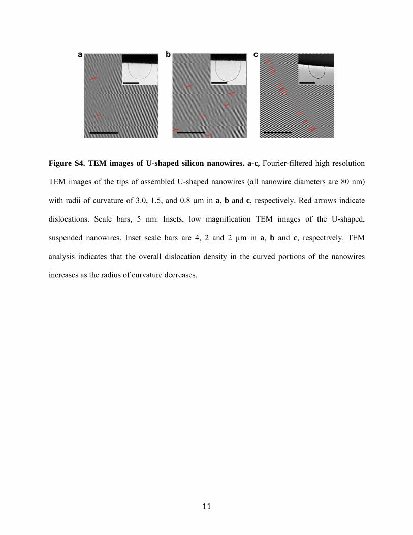
imaging (Figure 3c and Supplementary Video 1) revealed thatthe nanowire rapidly released most of the strain within 0.3 sand then further relaxed to a nearly straight configuration afterthe cutting process (Figure 3c, right). These results suggest thatbending is largely elastic for the assembly conditions. Second,high-resolution TEM images of suspended 80 nm diameternanowires with 3, 1.5, and 0.8 μm radii of curvature (Figure S4)show that dislocation density in the curved portions of thenanowires increases with reduced radius of curvature. Thesedata indicate that although strain in the nanowires is largelyelastic, an inelastic component is present for these strains,which is consistent with previous nanowire studies at highstrain levels.25
We have further investigated the nature of the strained U-shaped nanowires using Raman spectroscopy (SupportingInformation). Representative spectra recorded from 80 nmdiameter individual U-shaped nanowires with radii of curvature
from 3−0.8 μm and straight nanowires (i.e., not bent during theassembly process and cut by FIB to relax strain) suspendedfrom a free-standing mesh (Supporting Information) revealseveral key features (Figure 3d). The first-order scatteringpeaks centered at ∼520 cm−1 are consistent with bulk Si atpresent in all samples. However, the full width at half-maximum(fwhm) of this mode increases from 3.1 ± 0.2 cm−1 in as-grownstraight nanowires to 7.0 ± 0.6, 10.9 ± 2.4, and 14.9 ± 3.1 cm−1
as the radius of curvature decreases 3, 1.5, and 0.8 μm,respectively (N = 5; Figure 3e). Interestingly, following releaseby FIB-cutting, the fwhm returns to a value 3.3 ± 0.3 cm−1 (N= 5, Figure 3e), similar to unstrained nanowires, and is thusconsistent with SEM and TEM results described earlier.Previous studies26 indicate that the increases in fwhm can beattributed to compressive (positive frequency shift) and tensile(negative shift) strains present in bent semiconductor nano-wires, which both will be present in our U-shaped nanowires.
Figure 4. 3D U-shaped nanowire bioprobe arrays. (a) Photograph of a 3 in. wafer with deterministic 3D U-shaped nanowire probe arrays. Scale bar,10 mm. (b, c) Optical microscopy images of a representative region of 3D nanowire probe arrays. Scale bars are 200 and 20 μm in panels b and c,respectively. Two-hundred total devices were fabricated in four blocks with 50 devices per block. (d) Representative tilt-view SEM image of the tipsof 3D bend-up probe array. Scale bar, 10 μm. (e) Mapping of sensitivity-to-noise ratios of all 200 U-shaped silicon nanowire probes on the 3 in.wafer. 1, 2, 3, and 4 designate the four blocks. Each pixel (color from blue to red) indicates the sensitivity-to-noise (V−1) of individual devices; graypixels correspond to nonconductive devices.
Nano Letters Letter
DOI: 10.1021/acs.nanolett.6b00292Nano Lett. XXXX, XXX, XXX−XXX
E
Last, we demonstrate a potential application of shape-controlled deterministic nanowire assembly with design-based22
fabrication of large-scale three-dimensional (3D) nanowirebioprobe arrays. We targeted U-shaped silicon nanowires in a3D bend-up geometry since previous studies of 3D kinkednanowires highlighted the capability of these nanodevices forrecording intracellular action potentials.27 We note that overallfabrication (Supporting Information) is substantially simplifiedas all connections, including source/drain and interconnects,are made without the need to register to individual nanowiressince all alignments can be made relative to the original U-shaped trenches used for the deterministic assembly process. Aphotograph (Figure 4a) and optical microscopy images (Figure4b,c) highlight the regular structure of the probe chip with 200individually addressable nanodevices. A representative SEMimage of a portion of the probe tip region of the chip (Figure4d) shows the regular 3D U-shaped nanowire devices withpitch of ∼20 μm.Significantly, analysis of the device conductance values
showed that 181/200 devices were conducting, giving anabout 90% overall yield. Characterization of the water-gatetransconductance or sensitivity and sensitivity to noise ratio forthe 181 active nanodevices (Supporting Information) furtheryielded values for the mean ±1 standard deviation of 2.5 ± 2.0μS/V and 2.7 ± 1.2 × 10³ V−1, respectively. A map of thesensitivity to noise values (Figure 4e) highlights the high-yieldof high-sensitivity/noise devices, where 90% have values ≥ 500.These values are comparable to or better than the performanceof reported individual kinked nanowire devices28−30 and thusshould be capable of improved signal recording.In summary, we have demonstrated a new concept
combining simultaneous assembly and guided shaping toachieve large-scale, high-precision shape-controlled determin-istic assembly of nanowires. We lithographically pattern U-shaped trenches and then shear transfer nanowires to thepatterned substrate wafers, where the trenches serve to definethe positions and shapes of transferred nanowires. Studies usingsemicircular trenches have shown the capability for wafer-scaledeterministic assembly produced U-shaped nanowires withyields of ∼90% over nearly one-half million sites. In addition,mechanistic studies and simulations have shown that theshaping process results primarily in elastic deformation of thenanowires, and they have defined diameter-dependent limitsachievable for experimentally accessible forces. Last, thisapproach was used to assemble 3D U-shaped nanowire field-effect transistor bioprobe arrays containing 200 individuallyaddressable nanodevices with sensitivities suitable for actionpotential recording from electrogenic cells.27,28,30 In the future,we believe these 3D bioprobe arrays could be particularlyattractive for probing neural networks, including measurementsfrom acute brain slices,31 and possibly in vivo recording.32 Moregenerally, use of shape-controlled deterministic nanowireassembly to combine the strengths of wafer-scale top-downfabrication with diverse and tunable properties of one-dimensional building blocks in novel structural configurationsfor new functional integrated nanodevices based on nanowirestrain-engineering33,34 and possible directions has not yet beenimagined.
■ ASSOCIATED CONTENT*S Supporting InformationThe Supporting Information is available free of charge on theACS Publications website at DOI: 10.1021/acs.nano-lett.6b00292.
Materials and methods; dependence of nanowireanchoring yields on key trench dimensions; dependenceof nanowire bending curvature on contact pressure;dependence of nanowire bending curvature on nanowirediameter; TEM images of U-shaped silicon nanowires(PDF)SEM video recordings of the release process of a U-shaped silicon nanowire (AVI)
■ AUTHOR INFORMATIONCorresponding Author*E-mail: [email protected] ContributionsY.Z. and J.Y. contributed equally to this work.NotesThe authors declare no competing financial interest.
■ ACKNOWLEDGMENTSC.M.L. acknowledges support from Air Force Office ofScientific Research. L.M. acknowledges support from NationalBasic Research Program of China (2013CB934103), Interna-tional Science and Technology Corporation Program of China(2013DFA50840), and the National Natural Science Fund forDistinguished Young Scholars (51425204). M.N.M. acknowl-edges a Fannie and John Hertz Foundation GraduateFellowship and a NSF Graduate Research Fellowship. Thiswork was performed in part at the Center for NanoscaleSystems (CNS) of Harvard University.
■ REFERENCES(1) Lu, W.; Lieber, C. M. Nat. Mater. 2007, 6, 841−850.(2) Rutherglen, C.; Jain, D.; Burke, P. Nat. Nanotechnol. 2009, 4,811−819.(3) Yan, H.; Choe, H. S.; Nam, S. W.; Hu, Y.; Das, S.; Klemic, J. F.;Ellenbogen, J. C.; Lieber, C. M. Nature 2011, 470, 240−244.(4) Takei, K.; Takahashi, T.; Ho, J. C.; Ko, H.; Gillies, A. G.; Leu, P.W.; Fearing, R. S.; Javey, A. Nat. Mater. 2010, 9, 821−826.(5) LeMieux, M. C.; Roberts, M.; Barman, S.; Jin, Y. W.; Kim, J. M.;Bao, Z. Science 2008, 321, 101−104.(6) Lipomi, D. J.; Vosgueritchian, M.; Tee, B. C-K.; Hellstrom, S. L.;Lee, J. A.; Fox, C. H.; Bao, Z. Nat. Nanotechnol. 2011, 6, 788−792.(7) Wang, M. C. P.; Gates, B. D. Mater. Today 2009, 12, 34−43.(8) Druzhinina, T.; Hoeppener, S.; Schubert, U. S. Adv. Mater. 2011,23, 953−970.(9) Fan, Z.; Ho, J. C.; Jacobson, Z. A.; Yerushalmi, R.; Alley, R. L.;Razavi, H.; Javey, A. Nano Lett. 2008, 8, 20−25.(10) Tao, A.; Kim, F.; Hess, C.; Goldberger, J.; He, R.; Sun, Y.; Xia,Y.; Yang, P. Nano Lett. 2003, 3, 1229−1233.(11) Huang, Y.; Duan, X.; Wei, Q.; Lieber, C. M. Science 2001, 291,630−633.(12) Yu, G.; Cao, A.; Lieber, C. M. Nat. Nanotechnol. 2007, 2, 372−377.(13) Pauzauskie, P. J.; Radenovic, A.; Trepagnier, E.; Shroff, H.;Yang, P.; Liphardt, J. Nat. Mater. 2006, 5, 97−101.(14) Lee, M.; Im, J.; Lee, B. Y.; Myung, S.; Kang, J.; Huang, L.;Kwon, Y.-K.; Hong, S. Nat. Nanotechnol. 2006, 1, 66−71.(15) Cao, Q.; Han, S.; Tulevski, G. S.; Zhu, Y.; Lu, D. D.; Haensch,W. Nat. Nanotechnol. 2013, 8, 180−186.
Nano Letters Letter
DOI: 10.1021/acs.nanolett.6b00292Nano Lett. XXXX, XXX, XXX−XXX
F

(16) Park, H.; Afzali, A.; Han, S.-J.; Tulevski, G. S.; Franklin, A. D.;Tersoff, J.; Hannon, J. B.; Haensch, W. Nat. Nanotechnol. 2012, 7,787−791.(17) Agarwal, R.; Ladavac, K.; Roichman, Y.; Yu, G.; Lieber, C. M.;Grier, D. G. Opt. Express 2005, 13, 8906−8912.(18) Yao, J.; Yan, H.; Lieber, C. M. Nat. Nanotechnol. 2013, 8, 329−335.(19) Freer, E. M.; Grachev, O.; Duan, X.; Martin, S.; Stumbo, D. P.Nat. Nanotechnol. 2010, 5, 525−530.(20) Li, M.; Bhiladvala, R. B.; Morrow, T. J.; Sioss, J. A.; Lew, K.-K.;Redwing, J. M.; Keating, C. D.; Mayer, T. S. Nat. Nanotechnol. 2008, 3,88−92.(21) Rao, S. G.; Huang, L.; Setyawan, W.; Hong, S. Nature 2003, 425,36−37.(22) Yao, J.; Yan, H.; Das, S.; Klemic, J. F.; Ellenbogen, J. C.; Lieber,C. M. Proc. Natl. Acad. Sci. U. S. A. 2014, 111, 2431−2435.(23) Tang, D. M.; Ren, C.-L.; Wang, M.-S.; Wei, X.; Kawamoto, N.;Liu, C.; Bando, Y.; Mitome, M.; Fukata, N.; Golberg, D. Nano Lett.2012, 12, 1898−1904.(24) Superfine, R.; Falvo, M. R.; Clary, G. J.; Taylor, R. M.; Chi, V.;Brooks, F. P.; Washburn, S. Nature 1997, 389, 582−584.(25) Wang, L.; Zheng, K.; Zhang, Z.; Han, X. Nano Lett. 2011, 11,2382−2385.(26) Chen, J.; Conache, G.; Pistol, M.-E.; Gray, S. M.; Borgstrom, M.T.; Xu, H.; Xu, H. Q.; Samuelson, L.; Hakanson, U. Nano Lett. 2010,10, 1280−1286.(27) Tian, B.; Cohen-Karni, T.; Qing, Q.; Duan, X.; Xie, P.; Lieber,C. M. Science 2010, 329, 830−834.(28) Qing, Q.; Jiang, Z.; Xu, L.; Gao, R.; Mai, L.; Lieber, C. M. Nat.Nanotechnol. 2013, 9, 142−147.(29) Xu, L.; Jiang, Z.; Qing, Q.; Mai, L.; Zhang, Q.; Lieber, C. M.Nano Lett. 2013, 13, 746−751.(30) Xu, L.; Jiang, Z.; Mai, L.; Qing, Q. Nano Lett. 2014, 14, 3602−3607.(31) Qing, Q.; Pal, S. K.; Tian, B.; Duan, X.; Timko, B. P.; Cohen-Karni, T.; Murthy, V. N.; Lieber, C. M. Proc. Natl. Acad. Sci. U. S. A.2010, 107, 1882−1887.(32) Liu, J.; Fu, T.-M.; Cheng, Z. G.; Hong, G. S.; Zhou, T.; Jin, L.H.; Duvvuri, M.; Jiang, Z.; Kruskal, P.; Xie, C.; Suo, Z. G.; Fang, Y.;Lieber, C. M. Nat. Nanotechnol. 2015, 10, 629−636.(33) Sun, L.; Kim, D. H.; Oh, K. H.; Agarwal, R. Nano Lett. 2013, 13,3836−3842.(34) Cao, J.; Ertekin, E.; Srinivasan, V.; Fan, W.; Huang, S.; Zheng,H.; Yim, J. W. L.; Khanal, D. R.; Ogletree, D. F.; Grossman, J. C.; Wu,J. Nat. Nanotechnol. 2009, 4, 732−737.
Nano Letters Letter
DOI: 10.1021/acs.nanolett.6b00292Nano Lett. XXXX, XXX, XXX−XXX
G

1
Supporting Information for
Shape-Controlled Deterministic Assembly of Nanowires
Yunlong Zhao†, Jun Yao†, Lin Xu†,§, Max N. Mankin†, Yinbo Zhu⊥, Hengan Wu⊥, Liqiang Mai§,
Qingjie Zhang§ & Charles M. Lieber*,†,‡
†Department of Chemistry and Chemical Biology, and ‡Harvard John A. Paulson School of
Engineering and Applied Sciences, Harvard University, Cambridge, Massachusetts 02138,
United States
§State Key Laboratory of Advanced Technology for Materials Synthesis and Processing, Wuhan
University of Technology, Wuhan 430070, China
⊥CAS Key Laboratory of Mechanical Behavior and Design of Materials, Department of Modern
Mechanics, University of Science and Technology of China, Hefei, Anhui 230027, China
This file includes:
Materials and Methods
Supplementary Figures S1-S4
Supplementary Video-1 Description
Supplementary References

2
Materials and Methods
Nanowire synthesis. Silicon nanowires were synthesized using a gold (Au) nanoparticle-
catalysed vapour-liquid-solid (VLS) process described previously.1 Briefly, 10, 30 and 80 nm
diameter Au nanoparticles (15703, 15706 and 15710, Ted Pella, Redding, CA) were dispersed on
the SiO2 surface of Si growth substrates (600 nm thermal SiO2, Nova Electronic Materials,
Flower Mound, TX). Nanowire growth was carried out at 430–455 °C. Specifically, the intrinsic
nanowires were synthesized at a total pressure of 40 Torr with 2.5 standard cubic centimetres per
minute (sccm) silane (SiH4, 99.9999%, Voltaix, Branchburg, NJ) as the silicon reactant, 60 sccm
hydrogen (H2, 99.999%; Matheson, Basking Ridge, NJ) as the carrier gas. Growth temperatures
of 435 °C, 450 °C, and 450 °C were used for diameters of 10, 30, and 80 nm, respectively. For
the synthesis of p-type nanowires, additional 3.1 sccm diborane (B2H6, 100 p.p.m. in H2, Voltaix,
Branchburg, NJ) was introduced as the p-type dopant. Growth temperatures of 430 °C, 450 °C,
and 450 °C were used for diameters of 10, 30, and 80 nm, respectively. Intrinsic nanowires were
used for nanowire assembly and p-type nanowires were used for fabrication of bioprobe device
arrays in this work. Typical growth times of 1–2 h yielded nanowires with average lengths of
40–80 µm.
Shape controlled assembly. A range of target substrates were used in our studies, including Si
wafers (Nova Electronic Materials, Flower Mound, TX) with SiO2, Si3N4, Au, nickel (Ni) and
SU-8 polymer (SU-8 2000.5, Microchem, Inc., Westborough, MA) surface layers. The substrate
surface layer was cleaned by rinsing in isopropanol (IPA, Cleanroom® MB, KMG Electronic
Chemicals, Inc., Houston, TX) for 30 s followed by nitrogen drying. LOR 1A and diluted S1805
(1:2 (vol : vol) diluted in Thinner-P) (Microchem, Westborough, MA) for photolithography (PL)

3
or double layer polymethyl methacrylate (PMMA, 950-C2, Microchem, Westborough, MA) for
electron beam lithography (EBL) was spin-coated, and PL or EBL was used to define arrays of
trenches with thicknesses of ~260 nm and with shapes and widths as described in the main text.
For trenches with thicknesses of ~20, ~50, ~130, and ~260 nm, diluted PMMA 950-A2 (1:1 (vol :
vol) diluted in Anisole), PMMA 950-A2, PMMA 950-C2 and PMMA 950-A6 was spin-coated
as resist, respectively. The minimum radii of curvature trench structures fabricated by PL and
EBL were 1.5 m and 200 nm, respectively. No additional surface modification followed
exposure and development of these patterns.
Shape-controlled assembly of nanowires was carried out in a manner similar to shear-
printing described elsewhere.1-3 Briefly a target substrate patterned with an array of trenches was
mounted onto a micromanipulator-controlled moveable stage, covered with mineral oil (330760,
viscosity, v, ≈ 70 mPa•s, Sigma-Aldrich, St. Louis, MO), and then the nanowire growth
substrate was brought into contact with the target substrate with controlled contact pressure
(values in text). The target substrate was moved at a constant velocity of ~5 mm min-1 with
respect to the fixed nanowire growth substrate, and then the growth substrate was removed and
the target substrate rinsed with octane (98%, Sigma-Aldrich, St. Louis, MO) to remove the
lubricant. The minimum radius of nanowire curvature achievable by this process was determined
by using ca. 200 nm radii of curvature trenches fabricated by EBL for 80 and 30 nm diameter
silicon nanowires. For 10 nm diameter silicon nanowires, 76 +/- 1.1 nm (mean +/- standard
deviation) radius Au nanoparticles (15712, Ted Pella, Redding, CA; size statistics obtained from
the vendor’s characterization) were used as anchoring means. In this case, the Au nanoparticles
were dispersed on SiO2/Si substrate modified with poly-L-lysine (P8920, Sigma-Aldrich, St.
Louis, MO), followed by deposition of ~10 nm thick Al2O3 film by atomic layer deposition

4
(ALD) at 150oC (90 cycles). In addition, experiments were carried out by placing the nanowire
growth substrate directly over the substrate with trenches, translating approximately 100–200µm,
and then removing the growth substrate and imaging the positions of the transferred nanowires
with respect to the trenches; the data in Figure 2a was obtained in this manner.
TEM sample preparation and characterization. Arrays of U-shaped silicon nanowires with
different radii of curvature were prepared for transmission electron microscopy (TEM)
characterization by fixing the arms of the assembled wires between Au metal layers while
leaving the suspended nanowire tips exposed for imaging. We introduced Au layers on both top
and bottom of patterned PMMA for assembly as follows. (1) A Ni sacrificial layer (100 nm) was
deposited on an oxidized silicon substrate by thermal evaporation (TE). (2) A square mesh gold
ribbon network (100 nm) was defined on the Ni layer by EBL and TE. (3) Arrays of U-shaped 80
nm diameter silicon nanowires were patterned as described above such that the straight arms and
U-tips were on top of the gold mesh and open areas, respectively. (4) PMMA under the straight
arms of U-shaped nanowires was cross-linked by EBL using a dose of ~8,000 µC/cm2. (5) A
second Au mesh (100 nm thick) which was coincident in the x-y plane with the bottom mesh was
defined on top of the cross-linked PMMA and deposited via TE. (6) The nickel sacrificial layer
was etched in nickel etchant (TFB, Transene Company, Inc., Danvers, MA) for 1 h and then the
free-standing arrays of U-shaped silicon nanowires embedded in the Au-mesh/PMMA/Au-mesh
trilayer were transferred to a copper TEM grid (300 mesh Cu, Ted Pella, Redding, CA). TEM
characterization (JEOL 2100, JEOL Ltd. or aberration-corrected Zeiss Libra MC TEM, Carl
Zeiss AG) was carried out at a beam accelerating voltage of 200 kV. Fourier-filtered images

5
processed from the high-resolution TEM (HRTEM) images were used to characterize
dislocations in the bent nanowires.
Strain release tests. Arrays of suspended U-shaped silicon nanowires were transferred to TEM
grids as described above and introduced into a focused ion beam (FIB) instrument (dual
ion/electron beam Zeiss NVision 40, Carl Zeiss AG). The FIB was used to cut one of the two
suspended arms of a U-shaped nanowire (Ga+ ions, 30 kV) while monitoring the nanowire
release process in situ by SEM video-rate imaging(8 frames per second).
Raman spectroscopy characterization. Arrays of suspended U-shaped silicon nanowires with
some nanowires cut by FIB in a free-standing mesh supported on a Cu TEM grid were placed on
a glass slide. Straight nanowires that adhered in random positions on the PMMA surface (i.e., not
bent during the assembly process) were also transferred and suspended in the same mesh for
control measurements. Raman spectra were acquired with a LabRam Evolution Multiline Raman
Spectrometer (Horiba, Kyoto, Japan) equipped with 1800 blaze/mm grating and a 100x
microscope objective lens with numerical aperture (N.A.) of 0.95. A continuous-wave (CW)
diode laser with a wavelength of 633 nm was used as incident light source and circularly
polarized using a zero-order quarter waveplate optimized for 633 nm. The laser power was ~26
µW and the laser spot size was ~1.5 µm in diameter.
Finite element simulations of nanowire bending. A geometrically nonlinear finite element
model was used to simulate the large deformations of nanowires under load. The modelling and
simulations were carried out with commercial ANSYS 14.5 software. In our model, the nanowire

6
is considered as a linearly elastic cantilever beam with elastic modulus of 188 GPa and Poisson
ratio of 0.3 characteristic of silicon.4 The length and diameter of the cantilever beam are 20 μm
and 80 nm, respectively. The in-plane forces generated during the experimental assembly process
are expected to produce approximately uniform distributed bending loads, which are applied in
the simulations; these uniform bending loads ranged from 0 to 20 nN/μm. The deformation of the
nanowire under different loading is shown in Figure 2d. The corresponding load-dependent radii
of curvature at the fixed end were calculated from the simulated results and are plotted in Figure
2e.
Bend-up nanowire probe arrays. Arrays of U-shaped silicon nanowires were used as building
blocks to fabricate three-dimensional (3D) bend-up nanoprobe device arrays. Briefly, (1) a Ni
sacrificial layer (100 nm) was defined by EBL and deposited on a silicon substrate (600 nm
thermal SiO2). (2) The substrate was coated with SU-8 resist (1:1 diluted SU-8R 2000.5 in
cyclopentanone, Microchem, Inc., Westborough, MA), and then the bottom SU-8 support layer
was defined by EBL. (3) After definition of the U-shaped PMMA trench arrays by EBL, U-
shaped 10−80 nm diameter silicon nanowires were deterministically assembled in the trenches.
(4) Source/drain metal contacts Cr/Pd/Cr (1.5/75/50 nm) were defined by EBL and TE. Typically,
the source/drain contact separation was 1.5 μm in each probe, and the free end of the nanowire
extended 2−6 μm from the source contact. (5) A top SU-8 (SU-8R 2000.5, Microchem, Inc.,
Westborough, MA) layer was subsequently defined by EBL to complete the passivation of the
metal contacts/interconnects. (6) The nickel layer was etched (~1 h, TFB etchant, Transene
Company, Inc., Danvers, MA) to yield the 3D bend-up probes. The individual nanowire probe
devices were fabricated without registration to nanowires, since the patterns of bottom SU-8

7
passivation layer, contact electrodes and top SU-8 passivation layer, and x- and y- coordinates of
U-shaped nanowires all precisely match the original trench pattern used for U-shape
deterministic assembly; that is, the process follows a design-oriented fabrication approach.5
Device sensitivities were characterized by water-gate measurements in 1× phosphate
buffered saline (PBS) with a Ag/AgCl reference electrode.6-8 The nanowire device conductance
values were measured with a DC bias of 0.5 V, and the current was converted to voltage with a
current preamplifier (10-7 A/V, Model 1211, DL Instruments, Brooktondale, NY), and digitized
at 20 kHz sampling rate (Axon Digi1440A, Molecular Devices). The sensitivity of our U-shaped
silicon nanowires is 2.5 ± 2.0 µS/V. The sensitivity of our previous reported kinked silicon
nanowires6 is 8.5 ± 4.3µS/V.
8
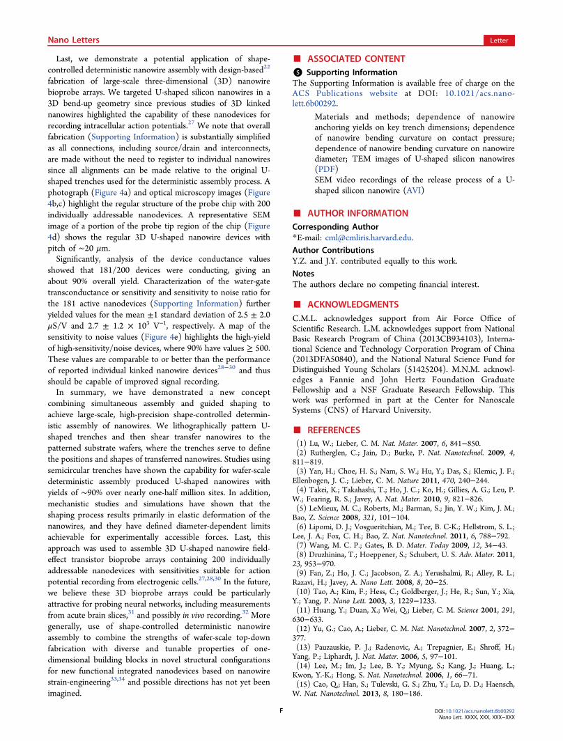
Figure S1. Dependence of nanowire anchoring yields on key trench dimensions. The
nanowire anchoring yield versus trench (a) width and (b) depth. For (a), trench widths are 0.5, 1,
2, 3, 4, 5 µm and depth is fixed at 260 nm. For each data point, statistics is based on analysis of
210 sites randomly selected. For (b), trench depths are 20, 50, 130, 260, 390 nm and width is
fixed at 3 µm. For each data point, statistics is based on analysis of 600 sites randomly selected.
The blue vertical dashed line corresponds to the 80 nm diameter nanowires used in the
measurements. These results indicate that trench width and depth can be used to optimize the
anchoring yield of nanowires during assembly.

9
Figure S2. Dependence of nanowire bending curvature on contact pressure. Representative
SEM images of 80 nm diameter silicon nanowires assembled with normal pressures of (a) 0.8, (b)
4.8 and (c) 7.2 N cm-2. Scale bars all 1 µm. These results are consistent with increasing in-plane
bending loads as the contact pressure is increased; that is, we find decreases in nanowire radius
of curvature with increasing bending loads (simulation) or transfer normal pressures
(experiments).

10
Figure S3. Dependence of nanowire bending curvature on nanowire diameter.
Representative SEM images of silicon nanowires with different diameters assembled with
normal pressures of 4.8 N cm-2. a, 10 nm diameter nanowires anchored on Au particles (radii
~75 nm). b, 30 nm diameter nanowire anchored on trenches with depth of 130 nm, width of 1µm,
and radii of inner curvature of 200 nm. c, 80 nm diameter nanowire anchored on trenches with
depth of 260 nm, width of 3 µm, and radii of inner curvature of 200 nm. Scale bars, 500 nm.
11
Figure S4. TEM images of U-shaped silicon nanowires. a-c, Fourier-filtered high resolution
TEM images of the tips of assembled U-shaped nanowires (all nanowire diameters are 80 nm)
with radii of curvature of 3.0, 1.5, and 0.8 µm in a, b and c, respectively. Red arrows indicate
dislocations. Scale bars, 5 nm. Insets, low magnification TEM images of the U-shaped,
suspended nanowires. Inset scale bars are 4, 2 and 2 µm in a, b and c, respectively. TEM
analysis indicates that the overall dislocation density in the curved portions of the nanowires
increases as the radius of curvature decreases.

12
Supplementary Video 1. SEM video recordings of the release process of a U-shaped silicon
nanowire. The radius of curvature of the U-shaped nanowire (diameter = 80 nm) assembled on a
copper TEM grid is 1.5 µm before cutting one arm with a FIB. After cutting the upper arm at the
position indicated by the green arrow, the nanowire springs back to an almost straight
configuration, suggesting that much of the strain introduced during U-shaped assembly of the
nanowires is elastic.

13
Supplementary References
1. Yao, J.; Yan, H.; Lieber, C. M. Nat. Nanotechnol. 2013, 8, 329–335.
2. Yan, H.; Choe, H. S.; Nam, S. W.; Hu, Y.; Das, S.; Klemic, J. F.; Ellenbogen, J. C.;
Lieber, C. M. Nature 2011, 470, 240–244.
3. Fan, Z.; Ho, J. C.; Jacobson, Z. A.; Yerushalmi, R.; Alley, R. L.; Razavi, H.; Javey, A.
Nano Lett. 2008, 8, 20–25.
4. Stan, G.; Krylyuk, S.; Davydov, A. V.; Cook, R. F. J. Mater. Res. 2012, 27, 562–570.
5. Yao, J.; Yan, H.; Das, S.; Klemic, J. F.; Ellenbogen, J. C.; Lieber, C. M. Proc. Natl.
Acad. Sci. U. S. A. 2014, 111, 2431–2435.
6. Qing, Q. Jiang, Z.; Xu, L.; Gao, R.; Mai, L.; Lieber, C. M. Nat. Nanotechnol. 2014, 9,
142–147.
7. Xu, L.; Jiang, Z.; Qing, Q.; Mai, L.; Zhang, Q.; Lieber, C. M. Nano Lett. 2013, 13, 746–
751.
8. Xu, L.; Jiang, Z.; Mai, L.; Qing, Q. Nano Lett. 2014, 14, 3602–3607.