sgls271a − october 2004 − revised june 2008 ... · sgls271a − october 2004 − revised june...
TRANSCRIPT

SGLS271A − OCTOBER 2004 − REVISED JUNE 2008
!"#$ % &'!!($ #% )'*+&#$ ,#$(- !,'&$% &!" $%)(&&#$% )(! $.( $(!"% (/#% %$!'"($% %$#,#!, 0#!!#$1- !,'&$ )!&(%%2,(% $ (&(%%#!+1 &+',( $(%$2 #++ )#!#"($(!%-
FEATURES Qualified for Automotive Applications
3.3-V Single-Supply Operation
Dual Simultaneous Sample-and-Hold Inputs
Differential or Single-Ended Analog Inputs Programmable Gain Amplifier: 0 dB to 18 dB
Separate Serial Control Interface
Single or Dual Parallel Bus Output
60-dB SNR at f IN = 10.5 MHz 73-dB SFDR at f IN = 10.5 MHz
Low Power: 275 mW
300-MHz Analog Input Bandwidth
3.3-V TTL/CMOS-Compatible Digital I/O Internal or External Reference
Adjustable Reference Input Range
Power-Down (Standby) Mode
TQFP-48 Package
APPLICATIONS Digital Communications (Baseband Sampling)
Portable Instrumentation
Video Processing
DESCRIPTIONThe ADS5204 is a dual 10-bit, 40 MSPS analog-to-digitalconverter (ADC). It simultaneously converts each analoginput signal into a 10-bit, binary coded digital word up toa maximum sampling rate of 40 MSPS per channel. Alldigital inputs and outputs are 3.3-V TTL/CMOScompatible.
An innovative dual pipeline architecture implemented ina CMOS process and the 3.3-V supply results in verylow power dissipation. In order to provide maximumflexibility, both top and bottom voltage references canbe set from user-supplied voltages. Alternatively, if noexternal references are available, the on-chip internalreferences can be used. Both ADCs share a commonreference to improve offset and gain matching. Ifexternal reference voltage levels are available, theinternal references can be powered downindependently from the rest of the chip, resulting in evengreater power savings.
The ADS5204 also features dual, onboard programmablegain amplifiers (PGAs) that allow a setting of 0 dB to 18 dBto adjust the gain of each set of inputs in order to matchthe amplitude of the incoming signal.
The ADS5204 is characterized for operation from −40°Cto +85°C and is available in a TQFP-48 package.
Please be aware that an important notice concerning availability, standard warranty, and use in critical applications of Texas Instrumentssemiconductor products and disclaimers thereto appears at the end of this data sheet.
www.ti.com
Copyright 2008, Texas Instruments Incorporated

SGLS271A − OCTOBER 2004 − REVISED JUNE 2008
www.ti.com
2
This integrated circuit can be damaged by ESD. Texas Instruments recommends that all integrated circuits be handledwith appropriate precautions. Failure to observe proper handling and installation procedures can cause damage.
ESD damage can range from subtle performance degradation to complete device failure. Precision integrated circuits may be moresusceptible to damage because very small parametric changes could cause the device not to meet its published specifications.
BLOCK DIAGRAM
ORDERING INFORMATION
PRODUCT PACKAGE−LEADPACKAGE
DESIGNATOR
SPECIFIEDTEMPERATURE
RANGE
PACKAGEMARKING
ORDERINGNUMBER
TRANSPORTMEDIA, QUANTITY
ADS5204 TQFP−48 PFB −40°C to +85°C AZ5204Q ADS5204IPFBRQ1 Tape and Reel, 1000
† For the most current package and ordering information, see the Package Option Addendum at the end of this document, or see the TI web siteat http://www.ti.com.
‡ Package drawings, thermal data, and symbolization are available at http://www.ti.com/packaging.
ABSOLUTE MAXIMUM RATINGS
ADS5204−Q1
AVDD to AGND,DVDD to DGND
Supply voltage
−0.5 V to 3.6 V
AVDD to DVDD,AGND to DGND
Supply voltage−0.5 V to 0.5 V
Digital input voltage range to DGND −0.5 V to DVDD + 0.5 V
Now Analog input voltage range to AGND −0.5 V to AVDD + 0.5 V
Now Digital output voltage applied from Ext. Source to DGND −0.5 V to DVDD + 0.5 V
VREFT, VREFB Reference voltage input range to AGND −0.5 V to AVDD + 0.5 V
TA Operating free−air temperature range (ADS5204I −40°C to 85°C
TSTG Storage temperature range −65°C to 150°C
Now Soldering temperature 1,6 mm (1/16 inch) from case for 10 seconds 300°C
(1) Stresses beyond those listed under “absolute maximum ratings” may cause permanent damage to the device. These are stress ratings only, andfunctional operation of the device at these or any other conditions beyond those indicated under “recommended operating conditions” is notimplied. Exposure to absolute-maximum-rated conditions for extended periods may affect device reliability.

SGLS271A − OCTOBER 2004 − REVISED JUNE 2008
www.ti.com
3
RECOMMENDED OPERATING CONDITIONSover operating free-air temperature range, TA, unless otherwise noted(1)
PARAMETER CONDITIONS MIN NOM MAX UNIT
POWER SUPPLY
AVDDDVDD Supply voltage 0 3.3 3.6 VDRVDD
Supply voltage 0 3.3 3.6 V
ANALOG AND REFERENCE INPUTS
VREFT Reference input voltage (top) fCLK = 1 MHz to 80 MHz 1.9 2 2.15 V
VREFB Reference input voltage (bottom) fCLK = 1 MHz to 80 MHz 0.95 1 1.1 V
VREFT–VREFB Reference voltage differential fCLK = 1 MHz to 80 MHz 0.95 1 1.1 V
RREF Reference input resistance fCLK = 80 MHz 1650 ΩIREF Reference input current fCLK = 80 MHz 0.62 mA
VIN Analog input voltage, differential −1 1 V
VIN Analog input voltage, single−ended(1) CML −1 CML +1 V
CI Analog input capacitance 8 pF
Clock input(2) 0 AVDD V
ANALOG OUTPUTS
CML voltage AVDD/2 V
CML output resistance 2.3 kΩDIGITAL INPUTS
VIH High-level input voltage 2.4 DVDD V
VIL Low-level input voltage DGND 0.8 V
Input capacitance 5 pF
tc (80 MHz) Clock period 12.5 ns
tw(CLKH), tw(CLKL)(80 MHz)
Pulse duration Clock high or low 5.25 ns
tc (40 MHz) Clock period 25 ns
tw(CLKH), tw(CLKL)(40 MHz)
Pulse duration Clock high or low 11.25 ns
(1) Applies only when the signal reference input connects to CML.(2) Clock pin is referenced to AVDD/AVSS.

SGLS271A − OCTOBER 2004 − REVISED JUNE 2008
www.ti.com
4
ELECTRICAL CHARACTERISTICSover recommended operating conditions with fCLK = 80MHz and use of internal voltage references, and PGA Gain = 0dB, unless otherwise noted.
PARAMETER TEST CONDITIONS MIN TYP MAX UNIT
POWER SUPPLY
AVDDAVDD = DVDD = DRVDD = 3.3 V,
64 72
DVDD IDD Operating Supply CurrentAVDD = DVDD = DRVDD = 3.3 V,CL = 10 pF, VIN = 3.5 MHz, −1 dBFS
1.7 2.2 mADRVDD
IDD Operating Supply Current CL = 10 pF, VIN = 3.5 MHz, −1 dBFS18 27
mA
PD Power DissipationPWDN_REF = ‘L’ 275 345
mWPD Power DissipationPWDN_REF = ‘H’ 240 300
mW
PD(STBY) Standby Power STDBY = ‘H’, CLK Held HIGH or LOW 125 175 µW
tPD Power-up time for all references from standby 550 ms
tWU Wake-up time External Reference 40 µs
DIGITAL INPUTS
IIH High-level input current on digital inputs include CLKAVDD = DVDD = DRVDD = 3.6 V
−1 1 µA
IIL Low-level input current on digital inputs include CLKAVDD = DVDD = DRVDD = 3.6 V
−1 1 µA
DIGITAL OUTPUTS
VOH High−level output voltageAVDD = DVDD = DRVDD = 3 V atIOH = 50 µA, Digital outputs forced HIGH
2.8 2.96 V
VOL Low-level output voltageAVDD = DVDD = DRVDD = 3 V atIOL = 50 µA, Digital outputs forced LOW
0.04 0.2 V
CO Output capacitance 5 pF
IOZH High- impedance state output current to high levelAVDD = DVDD = DRVDD = 3.6 V
−1 1 µA
IOZL High-impedance state output current to low levelAVDD = DVDD = DRVDD = 3.6 V
−1 1 µA
Data output rise and fall timeCLOAD = 10 pF, Single-bus mode 3 ns
Data output rise and fall timeCLOAD = 10 pF, Dual-bus mode 5 ns
REFERENCE OUTPUTS
VREFTO Reference top voltage Absolute Min/Max values valid and tested 1.85 2 2.1 V
VREFBO Reference bottom voltageAbsolute Min/Max values valid and testedfor AVDD = 3.3 V 0.925 1 1.05 V
REFT−REFB Differential reference voltage 0.925 1.0 1.05 V
DC ACCURACY
INL Integral nonlinearity, end point . Internal
(1) TA = −40°C to 85°C −1.5 ±0.4 1.5 LSBINL Integral nonlinearity, end point . Internalreferences(1) TA = −40°C to 85°C −1.5 ±0.4 1.5 LSB
DNL Differential nonlinearityInternalreferences(2) TA = −40°C to 85°C −0.9 ±0.4 1.0 LSB
Missing codes No Missing Codes Assured
Zero error(3)
AVDD = DVDD = DRVDD = 3.3 V0.12 ±1.5 %FS
Full-scale errorAVDD = DVDD = DRVDD = 3.3 VExternal References (3) 0.28 ±1.5 %FS
Gain errorExternal References (3)
0.24 ±1.5 %FS(1) Integral nonlinearity refers to the deviation of each individual code from a line drawn from zero to full-scale. The point used as zero occurs 1/2 LSB
before the first code transition. The full-scale point is defined as a level 1/2 LSB beyond the last code transition. The deviation is measured fromthe center of each particular code to the best-fit line between these two endpoints.
(2) Integral nonlinearity refers to the deviation of each individual code from a line drawn from zero to full-scale. The point used as zero occurs 1/2 LSBbefore the first code transition. The full-scale point is defined as a level 1/2 LSB beyond the last code transition. The deviation is measured fromthe center of each particular code to the best-fit line between these two endpoints.
(3) Zero error is defined as the difference in analog input voltage—between the ideal voltage and the actual voltage—that switches the ADC outputfrom code 0 to code 1. The ideal voltage level is determined by adding the voltage corresponding to 1/2 LSB to the bottom reference level. Thevoltage corresponding to 1 LSB is found from the difference of top and bottom references divided by the number of ADC output levels (1024).Full-scale error is defined as the difference in analog input voltage—between the ideal voltage and the actual voltage—that switches the ADCoutput from code 1022 to code 1023. The ideal voltage level is determined by subtracting the voltage corresponding to 1.5 LSB from the topreference level. The voltage corresponding to 1 LSB is found from the difference of top and bottom references divided by the number of ADC outputlevels (1024).

SGLS271A − OCTOBER 2004 − REVISED JUNE 2008
www.ti.com
5
DYNAMIC PERFORMANCE(1)TA = TMIN to TMAX, AVDD = DVDD = DRVDD = 3.3 V, fIN = −1 dBFS, Internal Reference, fCLK = 80 MHz, fS = 40 MSPS, Differential Input Range= 2 Vp−p, and PGA Gain = 0 dB, unless otherwise noted
PARAMETER TEST CONDITIONS MIN TYP MAX UNIT
fIN = 3.5 MHz 9.7 Bits
ENOB Effective number of bits fIN = 10.5 MHz 9.3 9.7 BitsENOB Effective number of bitsfIN = 20 MHz 9.6 Bits
fIN = 3.5 MHz −71 dB
THD Total harmonic distortion fIN = 10.5 MHz −71 −63 dBTHD Total harmonic distortionfIN = 20 MHz −68 dB
fIN = 3.5 MHz 60.5 dB
SNR Signal-to-noise ratio fIN = 10.5 MHz 60.5 dBSNR Signal-to-noise ratiofIN = 20 MHz 60 dB
fIN = 3.5 MHz 60 dB
SINAD Signal-to-noise ratio + distortion fIN = 10.5 MHz 57 60 dBSINAD Signal-to-noise ratio + distortionfIN = 20 MHz 60 dB
fIN = 3.5 MHz 75 dB
SFDR Spurious-free dynamic range fIN = 10.5 MHz 66 73 dBSFDR Spurious-free dynamic rangefIN = 20 MHz 70.5 dB
Analog input bandwidth See Note (2) 300 MHz
IMD 2-Tone intermodulation distortion f1 = 9.5 MHz, f2 = 9.9 MHz −68 dBc
A/B channel crosstalk −75 dBc
A/B channel offset mismatch 0.016 1.75 % of FS
A/B channel full-scale error mismatch 0.025 1 % of FS(1) These specifications refer to a 25-Ω series resistor and 15-pF differential capacitor between A/B+ and A/B− inputs; any source impedance brings
the bandwidth down.(2) Analog input bandwidth is defined as the frequency at which the sampled input signal is 3 dB down on unity gain and is limited by the input switch
impedance.
PGA SPECIFICATIONS
PARAMETER MIN TYP MAX UNIT
Gain Range 0 to 18 dB
Gain Step Size(1) 0.5826 dB
Gain Error(2) −0.15 ±0.025 0.15 dB
Control Bits Per Channel 5 Bits
(1) See Table 2, PGA Gain Code. Ideal step size: 18.0618 dB / 31 = 0.5826 dB(2) Deviation from ideal. See Table 2, all gain settings.

SGLS271A − OCTOBER 2004 − REVISED JUNE 2008
www.ti.com
6
PIN CONFIGURATION
Terminal FunctionsTERMINAL
I/O DESCRIPTIONNAME NO.
I/O DESCRIPTION
DRVDD 1,13 I Supply Voltage for Output Drivers
DRVSS 12, 24 I Digital Ground for Output Drivers
DA 9..0 14-23 O Data Outputs for Bus A. D9 is MSB. This is the primary bus. Data from both input channels can be output on this busor data from channel A only. The data outputs are in 3-state during power-down (see the Register Configuration table).
DB 9..0 2-11 O Data Outputs for Bus B. D9 is MSB. This is the second bus. Data is output from the B channel when dual bus outputmode is selected. The data outputs are in 3-state during power-down and single-bus modes (see the Timing Optionstable).
OE 48 I Output Enable. A low on this terminal will enable the data output bus, COUT and COUT.
COUT 26 O Latch Clock for the Data Outputs. COUT is in 3-state during power down.
COUT 25 O Inverted Latch Clock control for the Data Outputs. COUT is in 3-state during power down.
SDI 44 I Serial Data I/O
DVSS 43 I Digital Ground
CLK 47 I Clock Input. The input is sampled on each rising edge of CLK when using a 40-MHz input and alternate rising edgeswhen using an 80-MHz input. The clock pin is referenced to AVDD and AVSS to reduce noise coupling from digital logic.
DVDD 45 I Digital Supply Voltage
AVDD 27,37,41 I Analog Supply Voltage
CS 29 I Serial Data Registers Chip Select
AVSS 28,36,40 I Analog Ground
B− 35 I Negative Input for the Analog B Channel
B+ 34 I Positive Input for the Analog B Channel
REFT 31 I/O Reference Voltage Top. The voltage at this terminal defines the top reference voltage for the ADC. Sufficient filteringshould be applied to this input: the use of 0.1-µF capacitor between REFT and AVSS is highly recommended.Additionally a 0.1-µF capacitor should be connected between REFT and REFB.
REFB 30 I/O Reference Voltage Bottom. The voltage at this terminal defines the bottom reference voltage for the ADC. Sufficientfiltering should be applied to this input: the use of 0.1-µF capacitor between REFB and AVSS is recommended.Additionally, a 0.1-µF capacitor should be connected between REFT and REFB.
CML 32 O Common-Mode Level. This voltage is equal to (AVDD − AVSS)/2. An external capacitor of 0.1µF should be connectedbetween this terminal and AVSS when CML is used as a bias voltage. No capacitor is required if CML is not used.
PDWN_REF 33 I Power-Down for Internal Reference Voltages. A HIGH on this terminal disables the internal reference circuit.
STBY 42 I Standby Input. A high on this terminal powers down the device.
A− 39 I Negative Input for the Analog A Channel
A+ 38 I Positive Input for Analog A Channel
SCLK 46 I Serial Data Clock. Maximum clock rate is 20 MHz.

SGLS271A − OCTOBER 2004 − REVISED JUNE 2008
www.ti.com
7
TIMING REQUIREMENTS
PARAMETER TEST CONDITIONS MIN TYP MAX UNIT
fCLK Input clock rate 1 80 MHz
Conversion rate 1 40 MSPS
Clock duty cycle (40MHz) 45 50 55 %
Clock duty cycle (80MHz) 42 50 58 %
td(o) Output delay time CL = 10 pF 9 14 ns
ts(m) Mux setup time 9 10.4 ns
th(m) Mux hold time CL = 10 pF 1.7 2.1 ns
ts(o) Output setup time CL = 10 pF 9 10.4 ns
td(pipe) Pipeline delay (latency, channels A and B) MODE = 0, SELB = 0 8 CLK Cycles
td(pipe) Pipeline delay (latency, channels A and B) MODE = 1, SELB = 0 4 CLK Cycles
td(pipe) Pipeline delay (latency, channel A) MODE = 0, SELB = 1 8 CLK Cycles
td(pipe) Pipeline delay (latency, channel B) MODE = 0, SELB = 1 9 CLK Cycles
td(pipe) Pipeline delay (latency, channel A) MODE = 1, SELB = 1 8 CLK Cycles
td(pipe) Pipeline delay (latency, channel B) MODE = 1, SELB = 1 9 CLK Cycles
th(o) Output hold time CL = 10 pF 1.5 2.2 ns
td(a) Aperture delay time 3 ns
tJ(a) Aperture jitter 1.5 ps, rms
tdis Disable time, OE rising to Hi-Z 5 8 ns
ten Enable T\time, OE falling to valid data 5 8 ns
(1) All internal operations are performed at a 40-MHz clock rate.
SERIAL INTERFACE TIMING
PARAMETER MIN TYP MAX UNIT
fSCLK Maximum Clock Rate 20 MHz
tWH SCLK Pulse Width high 25 ns
tWH SCLK Pulse Width low 25 ns
tSU(CS_CK) Setup Time, CS low Before First Negative SCLK Edge 5 ns
tWH(CS) CS HIGH Width 10 ns
tSU(C16_CK) Setup Time, 16th Negative SCLK Edge before CS Rising Edge 5 ns
tSU(D) Setup Time, Data Ready Before SCLK Falling Edge 5 ns
tSU(H) Hold Time, Data Held Valid After SCLK Falling Edge 5 ns
TIMING OPTIONS
OPERATING MODE MODE SELB TIMING DIAGRAM FIGURE
80-MHz Input Clock, Dual-Bus Output, COUT = 40 MHz 0 0 1
40-MHz Input Clock, Dual-Bus Output, COUT = 40 MHz 1 0 2
80-MHz Input Clock, Single-Bus Output, COUT = 40 MHz 0 1 3
80-MHz Input Clock, Single-Bus Output, COUT = 80 MHz 1 1 4

SGLS271A − OCTOBER 2004 − REVISED JUNE 2008
www.ti.com
8
TIMING DIAGRAMS
Analog_A
Analog_B
DA[9:0]
DB[9:0]
DAB[19:0]
A1 A2 A3 A4 A5
B1 B2 B3 B4 B5
A1 A2 A3 A4 A5
B1 B2 B3 B4 B5
A&B 1 A&B 2 A&B 3 A&B 4 A&B 5
td(pipe)
t
td(o)
td(pipe)
ts(o) th(o)
0 1 2 3 4 5 6 7 8 9 10 11 12 13 14 15 16 17 18
Sample A1 and B1
DAB[19:0] is used to illustrate the placement of the busses DA and DB
ADCOUTA[9:0](3)
ADCOUTB[9:0](3)
COUT
COUT
d(o)
CLK(1)
CLK40INT(2)
(1) In this option CLK = 80 MHz.(2))CLK40INT refers to 40-MHz Internal Clock, per channel.(3))Internal signal only.
Figure 1. Dual Bus Output—Option 1
Sample A1 and B1
Analog_A
Analog_B
DA[9:0]
DB[9:0]
DAB[19:0]
A1 A2 A3 A4 A5
B1 B2 B3 B4 B5
A1 A2 A3 A4 A5
B1 B2 B3 B4 B5
A&B 1 A&B 2 A&B 3 A&B 4 A&B 5
td(o)
td(o)
ts(o) th(o)
td(pipe)
td(pipe)
8 9 101 2 3 4 5 6 7
DAB[19:0] is used to illustrate the combined busses DA and DB
ADCOUTA[9:0](2)
ADCOUTB[9:0](2)
COUT
COUT
CLK(1)
(1) In this option CLK = 40 MHz, per channel.(2))Internal signal only.
Figure 2. Dual Bus Output—Option 2

SGLS271A − OCTOBER 2004 − REVISED JUNE 2008
www.ti.com
9
Analog_A
Analog_B
DA[9:0]
A1 A2 A3 A4 A5
B1 B2 B3 B4 B5
A1 B1 A2 B2 A3 B3 A4 B4 A5 B5
td(pipe)
td(o)
td(pipe)
td(o)
th(o)
th(o)
ts(o)
ts(o)
0 1 2 3 4 5 6 7 8 9 10 11 12 13 14 15 16 17 18
Sample A1 and B1
ADCOUTA[9:0](3)
ADCOUTB[9:0](3)
COUT
COUT
CLK(1)
CLK40INT(2)
(1) In this option CLK = 80 MHz, per channel.(2))CLK40INT refers to 40-MHz internal Clock, per channel.(3))Internal signal only.
Figure 3. Single Bus Output—Option 1
Analog_A
Analog_B
DA[9:0]
A1 A2 A3 A4 A5
B1 B2 B3 B4 B5
A1 B1 A2 B2 A3 B3 A4 B4 A5 B5
td(pipe)
td(o)
td(pipe)
td(o)
ts(o)
th(o)
ts(m)
th(m)
0 1 2 3 4 5 6 7 8 9 10 11 12 13 14 15 16 17 18
Sample A1 and B1
ADCOUTA[9:0](3)
ADCOUTB[9:0](3)
COUT
COUT
CLK(1)
CLK40INT(2)
(1) In this option CLK = 80 MHz.(2))CLK40INT refers to 40-MHz internal Clock, per channel.(3))Internal signal only.
Figure 4. Single Bus Output—Option 2

SGLS271A − OCTOBER 2004 − REVISED JUNE 2008
www.ti.com
10
SCLK
CS
SDI
1 2 3 4 15 16
D15 D14 D13 D12 D01 D00D00
tSU(CS_CK)
tSU(D)
tH(D)
tSU(C16_CS)
tWH tWL
tWH(CS)
Figure 5. Serial Data Write
Table 1. Register Configuration
PGA4B
15
TWOS
14 13 12 11 10 9 8 7 6 5 4 3 2 1 0PGA0
APGA1
APGA2
APGA3
APGA4
APGA1
BPGA2
BPGA3
B00
Always write 0
SELBMODEPGA0
BReserved
Default (power up) condition for this register is all bits = 0.The user register is updated on either the first rising edgeof SCLK after the 16th falling edge or CS rising, whichevercomes first. Raising CS before 16 falling SCLK edgeshave been seen is an incomplete write error and noregister update occurs. The PGA gain settings areresynchronized to the internal data conversion clock toavoid data glitches caused by changing gain settingswhile sampling the inputs.
PGA gain control data is applied to the PGAs on thesecond falling edge of the ADC sample clock(CLK40INT) after a successful register write. Thisresynchronization ensures that no analog glitch occurseven when SCLK is asynchronous to CLK.
Note that only the PGA data is resynchronized. TheTWOS, MODE, and SELB register bits take effectimmediately after a successful register write.
OUTPUT DATA FORMATThe output data format can either be in Binary Two’sComplement ouput mode or in unsigned binary mode,which affects both A and B channels.
TWOS − Binary Two’s Complement Mode:
0 − Unsigned Binary
1 − Binary Two’s Complement Output.

SGLS271A − OCTOBER 2004 − REVISED JUNE 2008
www.ti.com
11
Table 2. PGA DB[0:4], 5−bit PGA gain code for channel A or B
GAIN (dB) PGx4 PGx3 PGx2 PGx1 PGx0
0 0 0 0 0 0
0.5606 0 0 0 0 1
1.1599 0 0 0 1 0
1.6643 0 0 0 1 1
2.3806 0 0 1 0 0
2.8703 0 0 1 0 1
3.5218 0 0 1 1 0
4.0824 0 0 1 1 1
4.6817 0 1 0 0 0
5.1630 0 1 0 0 1
5.8451 0 1 0 1 0
6.3903 0 1 0 1 1
6.9807 0 1 1 0 0
7.6040 0 1 1 0 1
8.0497 0 1 1 1 0
8.7712 0 1 1 1 1
9.2831 1 0 0 0 0
9.8272 1 0 0 0 1
10.4078 1 0 0 1 0
11.0301 1 0 0 1 1
11.7005 1 0 1 0 0
12.0412 1 0 1 0 1
12.7970 1 0 1 1 0
13.2208 1 0 1 1 1
14.0944 1 1 0 0 0
14.5400 1 1 0 0 1
15.0666 1 1 0 1 0
15.5630 1 1 0 1 1
16.1623 1 1 1 0 0
16.7229 1 1 1 0 1
17.4181 1 1 1 1 0
18.0618 1 1 1 1 1

SGLS271A − OCTOBER 2004 − REVISED JUNE 2008
www.ti.com
12
TYPICAL CHARACTERISTICS
At TA = 25°C, AVDD = DVDD = DRVDD = 3.3 V, fIN = −0.5 dBFS, Internal Reference, fCLK = 80 MHz, fS = 40 MSPS, Differential Input Range = 2 Vp-p,25-Ω series resistor, and 15-pF differential capacitor at A/B+ and A/B− inputs, unless otherwise noted.

SGLS271A − OCTOBER 2004 − REVISED JUNE 2008
www.ti.com
13
TYPICAL CHARACTERISTICS (Continued)
At TA = 25°C, AVDD = DVDD = DRVDD = 3.3 V, fIN = −0.5 dBFS, Internal Reference, fCLK = 80 MHz, fS = 40 MSPS, Differential Input Range = 2 Vp-p,25-Ω series resistor, and 15-pF differential capacitor at A/B+ and A/B− inputs, unless otherwise noted.

SGLS271A − OCTOBER 2004 − REVISED JUNE 2008
www.ti.com
14
PRINCIPLE OF OPERATIONThe ADS5204 implements a dual high-speed 10-bit,40MSPS converter in a cost-effective CMOS process.The differential inputs on each channel are sampledsimultaneously. Signal inputs are differential and the clocksignal is single-ended. The clock signal is either 80 MHzor 40 MHz, depending on the device configuration set bythe user. Powered from 3.3 V, the dual-pipeline designarchitecture ensures low-power operation and 10-bitresolution. The digital inputs are 3.3-V TTL/CMOScompatible. Internal voltage references are included forboth bottom and top voltages. Alternatively, the user mayapply externally generated reference voltages. In doingso, the input range can be modified to suit the application.
The ADC is a 5-stage pipelined ADC with four stages offully-differential switched capacitor sub-ADC/MDACpairs and a single sub-ADC in stage five. All stagesdeliver two bits of the final conversion result. A digitalerror correction is used to compensate for modestcomparator offsets in the sub-ADCs.
SAMPLE-AND-HOLD AMPLIFIER
Figure 6 shows the internal SHA/SHPGA architecture.The circuit is balanced and fully differential for goodsupply noise rejection. The sampling circuit has beenkept as simple as possible to obtain good performancefor high-frequency input signals.
Figure 6. SHA/SHPGA Architecture
The analog input signal is sampled on capacitors CSPand CSN while the internal device clock is low. Thesampled voltage is transferred to capacitors CHP andCHN and held on these while the internal device clockis high. The SHA can sample both single-ended anddifferential input signals.
The load presented to the AIN pin consists of theswitched input sampling capacitor CS (approximately2 pF) and its various stray capacitances. A simplifiedequivalent circuit for the switched capacitor input isshown in Figure 7. The switched capacitor circuit ismodeled as a resistor RIN. fCLK is the clock frequency,which is 40 MHz at full speed, and CS is the samplingcapacitor. The use of 25-Ω series resistors and adifferential 15-pF capacitor at the A/B+ and A/B− inputsis recommended to reduce noise.
NOTE: AIN can be any variation
of A or B inputs.
VCM = 0.5 (V(A/B+) + V(A/B−))
VCM
fCLK = 40MHz
Figure 7. Equivalent Circuit for the Switched Capacitor Input
ANALOG INPUT, DIFFERENTIALCONNECTION
The analog input of the ADS5204 is a differentialarchitecture that can be configured in various waysdepending on the signal source and the required levelof performance. A fully differential connection willdeliver the best performance from the converter. Theanalog inputs must not go below AVSS or above AVDD.The inputs can be biased with any common-modevoltage provided that the minimum and maximum inputvoltages stay within the range AVSS to AVDD. It isrecommended to bias the inputs with a common-modevoltage around AVDD/2. This can be accomplishedeasily with the output voltage source CML, which isequal to AVDD/2. CML is made available to the user tohelp simplify circuit design. This output voltage sourceis not designed to be a reference or to be loaded butmakes an excellent dc bias source and stays well withinthe analog input common-mode voltage range overtemperature.

SGLS271A − OCTOBER 2004 − REVISED JUNE 2008
www.ti.com
15
Table 3 lists the digital outputs for the correspondinganalog input voltages.
Table 3. Output Format for Differential Configuration
DIFFERENTIAL INPUT
VIN = (A/B+) – (A/B−), REFT − REFB = 1 V, PGA = 0 dB
ANALOG INPUT VOLTAGE DIGITAL OUTPUT CODE
VIN = +1 V 3FFHVIN = 0 200H
VIN = −1 V 000H
DC-COUPLED DIFFERENTIAL ANALOGINPUT CIRCUIT
Driving the analog input differentially can be achievedin various ways. Figure 8 gives an example where asingle-ended signal is converted into a differential signalby using a fully differential amplifier such as theTHS4141. The input voltage applied to VOCM of theTHS4141 shifts the output signal into the desiredcommon-mode level. VOCM can be connected to CMLof the ADS5204, the common-mode level is shifted toAVDD/2.
ADS5204
Figure 8. Single-Ended to Differential ConversionUsing the THS4141
AC-COUPLED DIFFERENTIAL ANALOGINPUT CIRCUIT
Driving the analog input differentially can be achieved byusing a transformer coupling, as illustrated in NO TAG.The center tap of the transformer is connected to thevoltage source CML, which sets the common-modevoltage to AVDD/2. No buffer is required at the output ofCML since the circuit is balanced and no current is drawnfrom CML.
ADS5204
Figure 9. AC-Coupled Differential Input withTransformer
ANALOG INPUT, SINGLE-ENDEDCONFIGURATION
For a single-ended configuration, the input signal isapplied to only one of the two inputs. The signal appliedto the analog input must not go below AVSS or aboveAVDD. The inputs can be biased with any common-modevoltage provided that the minimum and maximum inputvoltage stays within the range AVSS to AVDD. It isrecommended to bias the inputs with a common-modevoltage around AVDD/2. This can be accomplished easilywith the output voltage source CML, which is equal toAVDD/2. An example for this is shown in Figure 10.
ADS5204
Figure 10. AC-Coupled, Single-EndedConfiguration
The signal amplitude to achieve full-scale is 2 Vp-p. Thesignal, which is applied at A/B+ is centered at the biasvoltage. The input A/B− is also centered at the biasvoltage. The CML output is connected via a 4.7-kΩresistor to bias the input signal. There is a directdc-coupling from CML to A/B− while this input isac-decoupled through the 10-µF and 0.1-µF capacitors.The decoupling minimizes the coupling of A/B+ into theA/B− path.
SGLS271A − OCTOBER 2004 − REVISED JUNE 2008
www.ti.com
16
Table 4 lists the digital outputs for the correspondinganalog input voltages.
Table 4. Output Format for Single-Ended Configuration
SINGLE-ENDED INPUT, REFT − REFB = 1V, PGA = 0dB
ANALOG INPUT VOLTAGE DIGITAL OUTPUT CODE
V(A/B+) = VCML + 1V 3FFH
V(A/B+) = VCML 200HV(A/B+) = VCML − 1V 000H
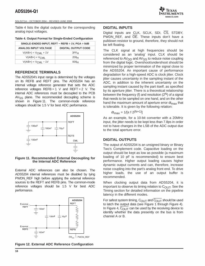
REFERENCE TERMINALSThe ADS5204’s input range is determined by the voltageson its REFB and REFT pins. The ADS5204 has aninternal voltage reference generator that sets the ADCreference voltages REFB = 1 V and REFT = 2 V. Theinternal ADC references must be decoupled to the PCBAVSS plane. The recommended decoupling scheme isshown in Figure 11. The common-mode referencevoltages should be 1.5 V for best ADC performance.
ADS5204
Figure 11. Recommended External Decoupling forthe Internal ADC Reference
External ADC references can also be chosen. TheADS5204 internal references must be disabled by tyingPWDN_REF high before applying the external referencesources to the REFT and REFB pins. The common-modereference voltages should be 1.5 V for best ADCperformance.
ADS5204
Figure 12. External ADC Reference Configuration
DIGITAL INPUTSDigital inputs are CLK, SCLK, SDI, CS, STDBY,PWDN_REF, and OE. These inputs don’t have apulldown resistor to ground, therefore, they should notbe left floating.
The CLK signal at high frequencies should beconsidered as an ‘analog’ input. CLK should bereferenced to AVDD and AVSS to reduce noise couplingfrom the digital logic. Overshoot/undershoot should beminimized by proper termination of the signal close tothe ADS5204. An important cause of performancedegradation for a high-speed ADC is clock jitter. Clockjitter causes uncertainty in the sampling instant of theADC, in addition to the inherent uncertainty on thesampling instant caused by the part itself, as specifiedby its aperture jitter. There is a theoretical relationshipbetween the frequency (f) and resolution (2N) of a signalthat needs to be sampled on one hand, and on the otherhand the maximum amount of aperture error dtmax thatis tolerable. It is given by the following relation:
dtmax = 1/[π f 2(N+1)]
As an example, for a 10-bit converter with a 20MHzinput, the jitter needs to be kept less than 7.8ps in ordernot to have changes in the LSB of the ADC output dueto the total aperture error.
DIGITAL OUTPUTSThe output of ADS5204 is an unsigned binary or BinaryTwo’s Complement code. Capacitive loading on theoutput should be kept as low as possible (a maximumloading of 10 pF is recommended) to ensure bestperformance. Higher output loading causes higherdynamic output currents and can, therefore, increasenoise coupling into the part’s analog front end. To drivehigher loads, the use of an output buffer isrecommended.
When clocking output data from ADS5204, it isimportant to observe its timing relation to COUT. See theTiming section for detailed information on the pipelinelatency in the different modes.
For safest system timing, COUT and COUT should be usedto latch the output data (see Figure 1 through Figure 4).In Figure 4, COUT can be used by the receiving device toidentify whether the data presently on the bus is fromchannel A or B.

SGLS271A − OCTOBER 2004 − REVISED JUNE 2008
www.ti.com
17
LAYOUT, DECOUPLING, AND GROUNDINGRULESProper grounding and layout of the PCB on which theADS5204 is populated is essential to achieve the statedperformance. It is advised to use separate analog anddigital ground planes that are spliced underneath the IC.The ADS5204 has digital and analog pins on oppositesides of the package to make this easier. Since there isno connection internally between analog and digitalgrounds, they have to be joined on the PCB. It isadvised to do this at one point in close proximity to theADS5204.
As for power supplies, separate analog and digital supplypins are provided on the part (AVDD/DVDD). The supply tothe digital output drivers is kept separate as well (DRVDD).Lowering the voltage on this supply to 3 V instead of thenominal 3.3 V improves performance because of thelower switching noise caused by the output buffers.Due to the high sampling rate and switched-capacitorarchitecture, the ADS5204 generates transients on thesupply and reference lines. Proper decoupling of theselines is, therefore, essential.
SERIAL INTERFACE
A falling edge on CS enables the serial interface,allowing the 16-bit control register date to be shifted(MSB first) on subsequent falling edges of SCLK. Thedata is loaded into the control register on the first risingedge of SCLK after its 16th falling edge or CS rising,whichever occurs first. CS rising before 16 falling SCLKedges have been counted is an error and the controlregister will not be updated.
The maximum update rate is:
NOTES1. Integral Nonlinearity (INL)— Integral nonlinearityrefers to the deviation of each individual code from a linedrawn from zero to full-scale. The point used as zerooccurs 1/2 LSB before the first code transition. Thefull-scale point is defined as a level 1/2 LSB beyond thelast code transition. The deviation is measured from thecenter of each particular code to the true straight linebetween these two endpoints.
2. Differential Nonlinearity (DNL)— An ideal ADCexhibits code transitions that are exactly 1 LSB apart. DNLis the deviation from this ideal value. Therefore, thismeasure indicates how uniform the transfer function stepsizes are. The ideal step size is defined here as the stepsize for the device under test [ i.e. (last transition level −
first transition level)/(2n − 2)]. Using this definition for DNLseparates the effects of gain and offset error. A minimumDNL better than –1LSB ensures no missing codes.
3. Zero and Full-Scale Error— Zero error is defined asthe difference in analog input voltage—between theideal voltage and the actual voltage—that switches theADC output from code 0 to code 1. The ideal voltagelevel is determined by adding the voltage correspondingto 1/5 LSB to the bottom reference level. The voltagecorresponding to 1 LSB is found from the difference oftop and bottom references divided by the number ofADC output levels (1024).
Full-scale error is defined as the difference in analog inputvoltage—between the ideal voltage and the actualvoltage—that switches the ADC output from code 1022 tocode 1023. The ideal voltage level is determined bysubtracting the voltage corresponding to 1. 5LSB from thetop reference level. The voltage corresponding to 1 LSBis found from the difference of top and bottom referencesdivided by the number of ADC output levels (1024).
4. Analog Input Bandwidth— The analog inputbandwidth is defined as the max. frequency of a 1-dBFSinput sine that can be applied to the device for which anextra 3-dB attenuation is observed in the reconstructedoutput signal.
5. Output Timing— Output timing td(o) is measuredfrom the 1.5-V level of the CLK input falling edge to the10%/90% level of the digital output. The digital outputload is not higher than 10 pF. Output hold time th(o) ismeasured from the 1.5-V level of the COUT input risingedge to the 10%/90% level of the digital output. Thedigital output is load is not less than 2 pF. Aperture delaytd(A) is measured from the 1.5-V level of the CLK inputto the actual sampling instant.
The OE signal is asynchronous. OE timing tdis ismeasured from the VIH(MIN) level of OE to the high-impedance state of the output data. The digital output loadis not higher than 10 pF. OE timing ten is measured fromthe VIL(MAX) level of OE to the instant when the outputdata reaches VOH(min) or VOL(max) output levels. Thedigital output load is not higher than 10 pF.6. Pipeline Delay (latency)— The number of clockcycles between conversion initiation on an input sampleand the corresponding output data being madeavailable from the ADC pipeline. Once the data pipelineis full, new valid output data is provided on every clockcycle. The first valid data is available on the output pinsafter the latency time plus the output delay time td(o)through the digital output buffers. Note that a minimumtd(o) is not assured because data can transition beforeor after a CLK edge. It is possible to use CLK for latchingdata, but at the risk of the prop delay varying overtemperature, causing data to transition one CLK cycle

SGLS271A − OCTOBER 2004 − REVISED JUNE 2008
www.ti.com
18
earlier or later. The recommended method is to use thelatch signals COUT and COUT which are designed toprovide reliable setup and hold times with respect to thedata out.7. Wake-Up Time— Wake-up time is from thepower-down state to accurate ADC samples being takenand is specified for external reference sources applied tothe device and an 80-MHz clock applied at the time ofrelease of STDBY. Cells that need to power up are thebandgap, bias generator, SHAs, and ADCs.
8. Power-Up Time— Power-up time is from thepower-down state to accurate ADC samples beingtaken with an 80-MHz clock applied at the time ofrelease of STDBY. Cells that need to power up are thebandgap, internal reference circuit, bias generator,SHAs, and ADCs.

PACKAGE OPTION ADDENDUM
www.ti.com 11-Mar-2011
Addendum-Page 1
PACKAGING INFORMATION
Orderable Device Status (1) Package Type PackageDrawing
Pins Package Qty Eco Plan (2) Lead/Ball Finish
MSL Peak Temp (3) Samples
(Requires Login)
ADS5204IPFBRG4Q1 ACTIVE TQFP PFB 48 1000 Green (RoHS& no Sb/Br)
CU NIPDAU Level-3-260C-168 HR
ADS5204IPFBRQ1 ACTIVE TQFP PFB 48 1000 Green (RoHS& no Sb/Br)
CU NIPDAU Level-3-260C-168 HR
(1) The marketing status values are defined as follows:ACTIVE: Product device recommended for new designs.LIFEBUY: TI has announced that the device will be discontinued, and a lifetime-buy period is in effect.NRND: Not recommended for new designs. Device is in production to support existing customers, but TI does not recommend using this part in a new design.PREVIEW: Device has been announced but is not in production. Samples may or may not be available.OBSOLETE: TI has discontinued the production of the device.
(2) Eco Plan - The planned eco-friendly classification: Pb-Free (RoHS), Pb-Free (RoHS Exempt), or Green (RoHS & no Sb/Br) - please check http://www.ti.com/productcontent for the latest availabilityinformation and additional product content details.TBD: The Pb-Free/Green conversion plan has not been defined.Pb-Free (RoHS): TI's terms "Lead-Free" or "Pb-Free" mean semiconductor products that are compatible with the current RoHS requirements for all 6 substances, including the requirement thatlead not exceed 0.1% by weight in homogeneous materials. Where designed to be soldered at high temperatures, TI Pb-Free products are suitable for use in specified lead-free processes.Pb-Free (RoHS Exempt): This component has a RoHS exemption for either 1) lead-based flip-chip solder bumps used between the die and package, or 2) lead-based die adhesive used betweenthe die and leadframe. The component is otherwise considered Pb-Free (RoHS compatible) as defined above.Green (RoHS & no Sb/Br): TI defines "Green" to mean Pb-Free (RoHS compatible), and free of Bromine (Br) and Antimony (Sb) based flame retardants (Br or Sb do not exceed 0.1% by weightin homogeneous material)
(3) MSL, Peak Temp. -- The Moisture Sensitivity Level rating according to the JEDEC industry standard classifications, and peak solder temperature.
Important Information and Disclaimer:The information provided on this page represents TI's knowledge and belief as of the date that it is provided. TI bases its knowledge and belief on informationprovided by third parties, and makes no representation or warranty as to the accuracy of such information. Efforts are underway to better integrate information from third parties. TI has taken andcontinues to take reasonable steps to provide representative and accurate information but may not have conducted destructive testing or chemical analysis on incoming materials and chemicals.TI and TI suppliers consider certain information to be proprietary, and thus CAS numbers and other limited information may not be available for release.
In no event shall TI's liability arising out of such information exceed the total purchase price of the TI part(s) at issue in this document sold by TI to Customer on an annual basis.
OTHER QUALIFIED VERSIONS OF ADS5204-Q1 :
• Catalog: ADS5204
NOTE: Qualified Version Definitions:

PACKAGE OPTION ADDENDUM
www.ti.com 11-Mar-2011
Addendum-Page 2
• Catalog - TI's standard catalog product

TAPE AND REEL INFORMATION
*All dimensions are nominal
Device PackageType
PackageDrawing
Pins SPQ ReelDiameter
(mm)
ReelWidth
W1 (mm)
A0(mm)
B0(mm)
K0(mm)
P1(mm)
W(mm)
Pin1Quadrant
ADS5204IPFBRG4Q1 TQFP PFB 48 1000 330.0 16.4 9.6 9.6 1.5 12.0 16.0 Q2
ADS5204IPFBRQ1 TQFP PFB 48 1000 330.0 16.4 9.6 9.6 1.5 12.0 16.0 Q2
PACKAGE MATERIALS INFORMATION
www.ti.com 14-Jul-2012
Pack Materials-Page 1

*All dimensions are nominal
Device Package Type Package Drawing Pins SPQ Length (mm) Width (mm) Height (mm)
ADS5204IPFBRG4Q1 TQFP PFB 48 1000 367.0 367.0 38.0
ADS5204IPFBRQ1 TQFP PFB 48 1000 367.0 367.0 38.0
PACKAGE MATERIALS INFORMATION
www.ti.com 14-Jul-2012
Pack Materials-Page 2

MECHANICAL DATA
MTQF019A – JANUARY 1995 – REVISED JANUARY 1998
POST OFFICE BOX 655303 • DALLAS, TEXAS 75265
PFB (S-PQFP-G48) PLASTIC QUAD FLATPACK
4073176/B 10/96
Gage Plane
0,13 NOM
0,25
0,450,75
Seating Plane
0,05 MIN
0,170,27
24
25
13
12
SQ
36
37
7,206,80
48
1
5,50 TYP
SQ8,809,20
1,050,95
1,20 MAX0,08
0,50 M0,08
0°–7°
NOTES: A. All linear dimensions are in millimeters.B. This drawing is subject to change without notice.C. Falls within JEDEC MS-026


IMPORTANT NOTICE
Texas Instruments Incorporated and its subsidiaries (TI) reserve the right to make corrections, enhancements, improvements and otherchanges to its semiconductor products and services per JESD46C and to discontinue any product or service per JESD48B. Buyers shouldobtain the latest relevant information before placing orders and should verify that such information is current and complete. Allsemiconductor products (also referred to herein as “components”) are sold subject to TI’s terms and conditions of sale supplied at the timeof order acknowledgment.
TI warrants performance of its components to the specifications applicable at the time of sale, in accordance with the warranty in TI’s termsand conditions of sale of semiconductor products. Testing and other quality control techniques are used to the extent TI deems necessaryto support this warranty. Except where mandated by applicable law, testing of all parameters of each component is not necessarilyperformed.
TI assumes no liability for applications assistance or the design of Buyers’ products. Buyers are responsible for their products andapplications using TI components. To minimize the risks associated with Buyers’ products and applications, Buyers should provideadequate design and operating safeguards.
TI does not warrant or represent that any license, either express or implied, is granted under any patent right, copyright, mask work right, orother intellectual property right relating to any combination, machine, or process in which TI components or services are used. Informationpublished by TI regarding third-party products or services does not constitute a license to use such products or services or a warranty orendorsement thereof. Use of such information may require a license from a third party under the patents or other intellectual property of thethird party, or a license from TI under the patents or other intellectual property of TI.
Reproduction of significant portions of TI information in TI data books or data sheets is permissible only if reproduction is without alterationand is accompanied by all associated warranties, conditions, limitations, and notices. TI is not responsible or liable for such altereddocumentation. Information of third parties may be subject to additional restrictions.
Resale of TI components or services with statements different from or beyond the parameters stated by TI for that component or servicevoids all express and any implied warranties for the associated TI component or service and is an unfair and deceptive business practice.TI is not responsible or liable for any such statements.
Buyer acknowledges and agrees that it is solely responsible for compliance with all legal, regulatory and safety-related requirementsconcerning its products, and any use of TI components in its applications, notwithstanding any applications-related information or supportthat may be provided by TI. Buyer represents and agrees that it has all the necessary expertise to create and implement safeguards whichanticipate dangerous consequences of failures, monitor failures and their consequences, lessen the likelihood of failures that might causeharm and take appropriate remedial actions. Buyer will fully indemnify TI and its representatives against any damages arising out of the useof any TI components in safety-critical applications.
In some cases, TI components may be promoted specifically to facilitate safety-related applications. With such components, TI’s goal is tohelp enable customers to design and create their own end-product solutions that meet applicable functional safety standards andrequirements. Nonetheless, such components are subject to these terms.
No TI components are authorized for use in FDA Class III (or similar life-critical medical equipment) unless authorized officers of the partieshave executed a special agreement specifically governing such use.
Only those TI components which TI has specifically designated as military grade or “enhanced plastic” are designed and intended for use inmilitary/aerospace applications or environments. Buyer acknowledges and agrees that any military or aerospace use of TI componentswhich have not been so designated is solely at the Buyer's risk, and that Buyer is solely responsible for compliance with all legal andregulatory requirements in connection with such use.
TI has specifically designated certain components which meet ISO/TS16949 requirements, mainly for automotive use. Components whichhave not been so designated are neither designed nor intended for automotive use; and TI will not be responsible for any failure of suchcomponents to meet such requirements.
Products Applications
Audio www.ti.com/audio Automotive and Transportation www.ti.com/automotive
Amplifiers amplifier.ti.com Communications and Telecom www.ti.com/communications
Data Converters dataconverter.ti.com Computers and Peripherals www.ti.com/computers
DLP® Products www.dlp.com Consumer Electronics www.ti.com/consumer-apps
DSP dsp.ti.com Energy and Lighting www.ti.com/energy
Clocks and Timers www.ti.com/clocks Industrial www.ti.com/industrial
Interface interface.ti.com Medical www.ti.com/medical
Logic logic.ti.com Security www.ti.com/security
Power Mgmt power.ti.com Space, Avionics and Defense www.ti.com/space-avionics-defense
Microcontrollers microcontroller.ti.com Video and Imaging www.ti.com/video
RFID www.ti-rfid.com
OMAP Mobile Processors www.ti.com/omap TI E2E Community e2e.ti.com
Wireless Connectivity www.ti.com/wirelessconnectivity
Mailing Address: Texas Instruments, Post Office Box 655303, Dallas, Texas 75265Copyright © 2012, Texas Instruments Incorporated