sgd gktw70snae4ed datasheet - datadisplay group gktw70snae4ed sg-01-005 product specification model:...
TRANSCRIPT

The information contained in this document has been carefully researched and is, to the best
of our knowledge, accurate. However, we assume no liability for any product failures or
damages, immediate or consequential, resulting from the use of the information provided
herein. Our products are not intended for use in systems in which failures of product could
result in personal injury. All trademarks mentioned herein are property of their respective
owners. All specifications are subject to change without notice.
Datasheet
SGD GKTW70SNAE4ED
SG-01-005

P r o d u c t S p e c i f i c a t i o n
Model: GKTW70SNAE4ED
Rev. No. Issued Date. Page.
A 2012, Jan. 19 1 / 25
Thin-Film-Transistor LCD Module Model: GKTW70SNAE4ED
Acceptance
Solomon Goldentek Display Corp. NO. 18 Ta-Yeh St., Ta-Fa Industrial Park,Ta-Liao Hsiang, Kaohsiung Hsien 831, TAIWAN , R.O.C.
FAX: 886-7-7886800
Approved and Checked by
Approved by Checked by Made by

P r o d u c t S p e c i f i c a t i o n
Model: GKTW70SNAE4ED
Rev. No. Issued Date. Page.
A 2012, Jan. 19 2 / 25
Revise Records
Rev. Date Contents Written Approved
A 2012/01/19 Preliminary Specification Aron Jau James Lu
Special Notes
Note1.
Note2.
Note3.
Note4.
Note5.

P r o d u c t S p e c i f i c a t i o n
Model: GKTW70SNAE4ED
Rev. No. Issued Date. Page.
A 2012, Jan. 19 3 / 25
Contents
1. General Description and Features .......................................................... 4 1.1 Features 4 1.2 LCD Module 4 2. Mechanical Information .......................................................................... 4 3. Electrical Specifications .......................................................................... 5 3.1 Absolute Max. Ratings 5 3.2 LVDS Switching Characteristics 11 4. Optical Characteristics ......................................................................... 13 4.1 Optical characteristic of the LCD 13 5. I/O Terminal .......................................................................................... 16 5.1 Pin Assignment 16 5.2 Back-light Dimming 17 5.3 Block Diagram 18 6. Display Color and Input Data ................................................................ 19 7. Reliability Condition .............................................................................. 20 8. Dimensional Outlines ............................................................................ 21 9. Incoming Inspection Standards ........................................................... 22

P r o d u c t S p e c i f i c a t i o n
Model: GKTW70SNAE4ED
Rev. No. Issued Date. Page.
A 2012, Jan. 19 4 / 25
1. General Description and Features
GKTW70SNAE4ED is a transmissive type color active matrix TFT (Thin Film Transistor) liquid crystal display (LCD) that uses amorphous silicon TFT as a switching device. This model is composed of a TFT-LCD module, a receiver circuit, and a back-light unit. Graphics and texts can be displayed on a WVGA 800 (W) x 3 x 480 (H) dots (16:9 aspect ratio) with 262,144 colors by supplying 18 bits data signal (6bits/each color). The following table described the features of GKTW70SNAE4ED. 1.1 Features
- Transmissive and back-light with 27 LEDs are available. - TN (Twisted Nematic) mode. - LVDS Receiver 18 bit Interface. - Back-light Dimming control
1.2 LCD Module
Item Specification Unit
Screen Size 7.0 inches Diagonal
Display Resolution 800 (H) x 480 (V) Pixel
Active Area 153.6 (H) x 86.64 (V) mm
Outline Dimension 165.00 (H) x 104.00 (V) x 5.4 (T) mm
Display Mode Normally white mode/ Transmissive --
Surface Treatment Anti-glare(AG) --
Pixel Arrangement R,G,B Vertical Stripe --
Pixel Size 192 x 180.5 um
Display Color 262k --
Viewing Direction 6 o’clock --
Input Interface LVDS Receiver 18 bit Interface --
2. Mechanical Information
Item Min. Typ. Max. Unit Note
Module Size
Horizontal (H) -- 165.00 -- mm
Vertical (V) -- 104.00 -- mm
Thickness (T) -- 5.4 -- mm (1)
Weight -- (150) -- g --
Note (1) Not Include Component. Refer to the Outline Dimension Drawing as attached.

P r o d u c t S p e c i f i c a t i o n
Model: GKTW70SNAE4ED
Rev. No. Issued Date. Page.
A 2012, Jan. 19 5 / 25
3. Electrical Specifications 3.1 Absolute Max. Ratings
3.1.1 Absolute Ratings of Environment If the operating condition exceeds the following absolute maximum ratings, the TFT LCD module may be damaged permanently.
(Ta=252°C, VSS=GND=0)
Item Symbol Min. Max. Unit Note
Storage temperature TSTG -30 80 °C (1)
Operating temperature TOPR -20 70 °C (1,2,3)
Note (1) 95 % RH Max. ( 40 °C ≥ Ta ). Maximum wet-bulb temperature at 39 °C or less. (Ta > 40 °C) No condensation.
Note (2) In case of below 0°, the response time of liquid crystal (LC) becomes slower and the color of panel becomes darker than normal one. Level of retardation depends on temperature, because of LC's character
Note (3) Only operation is guarantied at operating temperature. Contrast, response time, another display quality are evaluated at +25°C.

P r o d u c t S p e c i f i c a t i o n
Model: GKTW70SNAE4ED
Rev. No. Issued Date. Page.
A 2012, Jan. 19 6 / 25
3.1.2 Electrical Absolute Maximum Ratings
(VSS=GND=0)
Parameter Symbol Min. Max. Unit Remark
Power supply Logic voltage VCC -0.3 4.0 V
Power supply LED voltage VLED -0.3 6.0 V
Permissive input ripple voltage VRF -- 100 mVp-p VCC=+3.0V
Display On/Off Sequence :

P r o d u c t S p e c i f i c a t i o n
Model: GKTW70SNAE4ED
Rev. No. Issued Date. Page.
A 2012, Jan. 19 7 / 25
3.1.3 DC Electrical Characteristics of the TFT LCD
(Ta=252°C, VSS=GND=0)
Item Symbol Min. Typ. Max. Unit Remark
Power supply Logic Voltage VCC 3.0 3.3 3.6 V
Power supply LED Voltage VLED 4.5 5 5.5 V
Input Voltage for logic
H Level VIH 0.7xVCC - VCC V
L Level VIL 0 - 0.3xVCC V
Power Supply current ICC - (170) - mA Note 1
Power Supply current ILED - 450 600 mA
LED Life time - (30000) - - Hr Note 2
Note1: fv =60Hz , Ta=25°C , Display pattern : Black pattern
Note2: The environmental conducted under ambient air flow ,at Ta=25±2°C,60%RH±5%
P r o d u c t S p e c i f i c a t i o n
Model: GKTW70SNAE4ED
Rev. No. Issued Date. Page.
A 2012, Jan. 19 8 / 25
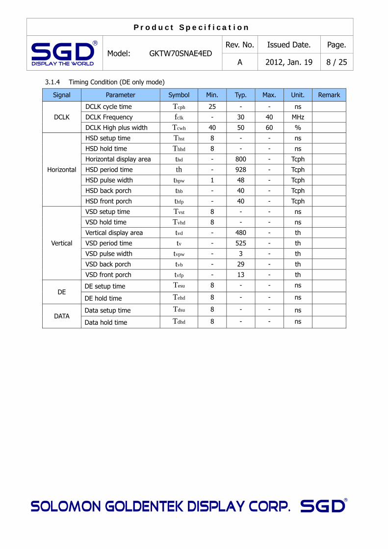
3.1.4 Timing Condition (DE only mode)
Signal Parameter Symbol Min. Typ. Max. Unit. Remark
DCLK
DCLK cycle time Tcph 25 - - ns
DCLK Frequency fclk - 30 40 MHz
DCLK High plus width Tcwh 40 50 60 %
Horizontal
HSD setup time Thst 8 - - ns
HSD hold time Thhd 8 - - ns
Horizontal display area thd - 800 - Tcph
HSD period time th - 928 - Tcph
HSD pulse width thpw 1 48 - Tcph
HSD back porch thb - 40 - Tcph
HSD front porch thfp - 40 - Tcph
Vertical
VSD setup time Tvst 8 - - ns
VSD hold time Tvhd 8 - - ns
Vertical display area tvd - 480 - th
VSD period time tv - 525 - th
VSD pulse width tvpw - 3 - th
VSD back porch tvb - 29 - th
VSD front porch tvfp - 13 - th
DE DE setup time Tesu 8 - - ns
DE hold time Tehd 8 - - ns
DATA Data setup time Tdsu 8 - - ns
Data hold time Tdhd 8 - - ns

P r o d u c t S p e c i f i c a t i o n
Model: GKTW70SNAE4ED
Rev. No. Issued Date. Page.
A 2012, Jan. 19 9 / 25
3.1.5 Timing Characteristic 3.1.5.1 DE and RGB Input Timing

P r o d u c t S p e c i f i c a t i o n
Model: GKTW70SNAE4ED
Rev. No. Issued Date. Page.
A 2012, Jan. 19 10 / 25

P r o d u c t S p e c i f i c a t i o n
Model: GKTW70SNAE4ED
Rev. No. Issued Date. Page.
A 2012, Jan. 19 11 / 25
3.2 LVDS Switching Characteristics 3.2.1 LVDS Timing Condition
Symbol Parameter Min. Typ. Max. Unit. Note
tRCP CLK OUT Period VCC = 3.0 - 3.6V 11.76 T 50.0 ns
VCC = 2.5 - 3.6V 14.28 T 50.0 ns
tRCH CLK OUT High Time - 4T/7 - ns
tRCL CLK OUT Low Time - 3T/7 - ns
tRCD RCLK +/- to CLK OUT Delay - 5T/7 - ns
tRS TTL Data Setup to CLK OUT 0.35T-0.3 - - ns
tRH TTL Data Hold from CKL OUT 0.45T-1.6 - - ns
tTLH TTL Low to High Transition Time - 2.0 3.0 ns
tTHL TTL High to Low Transition Time - 1.8 3.0 ns
tRIP1 Input Data Position0 (T = 11.76ns) -0.4 0.0 0.4 ns
tRIP0 Input Data Position1 (T = 11.76ns) T/7-0.4 T/7 T/7+0.4 ns
tRIP6 Input Data Position2 (T = 11.76ns) 2T/7-0.4 2T/7 2T/7+0.4 ns
tRIP5 Input Data Position3 (T = 11.76ns) 3T/7-0.4 3T/7 3T/7+0.4 ns
tRIP4 Input Data Position4 (T = 11.76ns) 4T/7-0.4 4T/7 4T/7+0.4 ns
tRIP3 Input Data Position5 (T = 11.76ns) 5T/7-0.4 5T/7 5T/7+0.4 ns
tRIP2 Input Data Position6 (T = 11.76ns) 6T/7-0.4 6T/7 6T/7+0.4 ns
tRPLL Phase Lock Loop Set 10.0 ms

P r o d u c t S p e c i f i c a t i o n
Model: GKTW70SNAE4ED
Rev. No. Issued Date. Page.
A 2012, Jan. 19 12 / 25
3.2.2 LVDS AC Timing

P r o d u c t S p e c i f i c a t i o n
Model: GKTW70SNAE4ED
Rev. No. Issued Date. Page.
A 2012, Jan. 19 13 / 25
4. Optical Characteristics 4.1 Optical characteristic of the LCD The following items are measured under stable conditions. The optical characteristics should be measured in a dark room or equivalent state with the methods. Measuring equipment: BM-7A
Item Symbol Condition Min Type Max Unit Note
Brightness B (500) (550) -- cd/m2
Response time Tr
=0 - 5 7 ms
. Tf -- 20 28 ms
Contrast ratio CR
At optimized viewing angle
(400) (500) -- --
Luminance Uniformity ΔL 70 80 %
Color Chromaticity (CIE 1931)
White Wx =0
Normal Viewing Angle
(0.280) (0.310) (0.340) -- BM-7A
Wy (0.330) (0.360) (0.390)
Viewing Angle (6H)
Hor. R
CR10
60 70 --
Degree L 60 70 --
Ver. U 40 50 --
D 50 60 --

P r o d u c t S p e c i f i c a t i o n
Model: GKTW70SNAE4ED
Rev. No. Issued Date. Page.
A 2012, Jan. 19 14 / 25
a. Test equipment setup
After stabilizing and leaving the panel alone shall be warmed up for the stable operation of LCM, the measurement should be executed. Measurement should be executed in a stable, windless, and dark room. Optical specifications are measured by Topcon BM-7A(fast) with a viewing angle of 2 at a distance of 50cm and normal direction.
b. Definition of response time: Tr and Tf
The response time is defined as the following figure and shall be measured by switching the input signal for “black” and “white”.
c. Definition of contrast ratio:
Brightness measured when LCD is at “white state”
Contrast Ratio (CR) =
Brightness measured when LCD is at “black state”
d. Measured at the center area of the panel when all the input terminals of LCD panel are electrically
opened.

P r o d u c t S p e c i f i c a t i o n
Model: GKTW70SNAE4ED
Rev. No. Issued Date. Page.
A 2012, Jan. 19 15 / 25
e. View Angle
f. Definition of Luminance of White: Luminance of white at the center points
Light Source of Back-Light Unit LED Type
g. Definition of White Uniformity
Min. luminance of white among 9-pointsWhite Uniformity = X 100%
Max. luminance of white among 9-points

P r o d u c t S p e c i f i c a t i o n
Model: GKTW70SNAE4ED
Rev. No. Issued Date. Page.
A 2012, Jan. 19 16 / 25
5. I/O Terminal 5.1 Pin Assignment
Pin No. Symbol I/O Function Remark
1 VCC P Power Supply Logic voltage +3.3V
2 VCC P Power Supply Logic voltage +3.3V
3 VSS P Ground
4 VSS P Ground
5 RIN0- I Negative LVDS differential data input
6 RIN0+ I Positive LVDS differential data input
7 VSS P Ground
8 RIN1- I Negative LVDS differential data input
9 RIN1+ I Positive LVDS differential data input
10 VSS P Ground
11 RIN2- I Negative LVDS differential data input
12 RIN2+ I Positive LVDS differential data input
13 VSS P Ground
14 RCLK- I Negative LVDS differential clock input
15 RCLK+ I Positive LVDS differential clock input
16 VSS P Ground
17 VLED P Power Supply LED voltage +5V
18 VLED P Power Supply LED voltage +5V
19 ADJ I Back-light Dimming control
20 VSS P Ground
I: Input, O: Output, P: Power Notes: 1) VSS Pin must ground contact, can not be floating.

P r o d u c t S p e c i f i c a t i o n
Model: GKTW70SNAE4ED
Rev. No. Issued Date. Page.
A 2012, Jan. 19 17 / 25
5.2 Back-light Dimming Note 2: ADJ signal=0~3.3V, Operating frequency:1KHz

P r o d u c t S p e c i f i c a t i o n
Model: GKTW70SNAE4ED
Rev. No. Issued Date. Page.
A 2012, Jan. 19 18 / 25
5.3 Block Diagram

P r o d u c t S p e c i f i c a t i o n
Model: GKTW70SNAE4ED
Rev. No. Issued Date. Page.
A 2012, Jan. 19 19 / 25
6. Displayed Color and Input Data
Color & Gray Scale
Data Signal R5 R4 R3 R2 R1 R0 G5 G4 G3 G2 G1 G0 B5 B4 B3 B2 B1 B0
Basic Color
Black 0 0 0 0 0 0 0 0 0 0 0 0 0 0 0 0 0 0 Red(0) 1 1 1 1 1 1 0 0 0 0 0 0 0 0 0 0 0 0 Green(0) 0 0 0 0 0 0 1 1 1 1 1 1 0 0 0 0 0 0 Blue(0) 0 0 0 0 0 0 0 0 0 0 0 0 1 1 1 1 1 1 Cyan 0 0 0 0 0 0 1 1 1 1 1 1 1 1 1 1 1 1 Magenta 1 1 1 1 1 1 0 0 0 0 0 0 1 1 1 1 1 1 Yellow 1 1 1 1 1 1 1 1 1 1 1 1 0 0 0 0 0 0 White 1 1 1 1 1 1 1 1 1 1 1 1 1 1 1 1 1 1
Red
Black 0 0 0 0 0 0 0 0 0 0 0 0 0 0 0 0 0 0 Red(62) 0 0 0 0 0 1 0 0 0 0 0 0 0 0 0 0 0 0 Red(61) 0 0 0 0 1 0 0 0 0 0 0 0 0 0 0 0 0 0 : : : : : : : : : : : : : : : : : : : Red(31) 0 1 1 1 1 1 0 0 0 0 0 0 0 0 0 0 0 0 : : : : : : : : : : : : : : : : : : : Red(1) 1 1 1 1 1 0 0 0 0 0 0 0 0 0 0 0 0 0 Red(0) 1 1 1 1 1 1 0 0 0 0 0 0 0 0 0 0 0 0
Green
Black 0 0 0 0 0 0 0 0 0 0 0 0 0 0 0 0 0 0 Green(62) 0 0 0 0 0 0 0 0 0 0 0 1 0 0 0 0 0 0 Green(61) 0 0 0 0 0 0 0 0 0 0 1 0 0 0 0 0 0 0 : : : : : : : : : : : : : : : : : : : Green(31) 0 0 0 0 0 0 0 1 1 1 1 0 0 0 0 0 0 0 : : : : : : : : : : : : : : : : : : : Green(1) 0 0 0 0 0 0 1 1 1 1 1 0 0 0 0 0 0 0 Green(0) 0 0 0 0 0 0 1 1 1 1 1 1 0 0 0 0 0 0
Blue
Black 0 0 0 0 0 0 0 0 0 0 0 0 0 0 0 0 0 0 Blue(62) 0 0 0 0 0 0 0 0 0 0 0 0 0 0 0 0 0 1 Blue(61) 0 0 0 0 0 0 0 0 0 0 0 0 0 0 0 0 1 0 : : : : : : : : : : : : : : : : : : : Blue(31) 0 0 0 0 0 0 0 0 0 0 0 0 0 1 1 1 1 1 : : : : : : : : : : : : : : : : : : : Blue(1) 0 0 0 0 0 0 0 0 0 0 0 0 1 1 1 1 1 0 Blue(0) 0 0 0 0 0 0 0 0 0 0 0 0 1 1 1 1 1 1
0 : Low level voltage, 1 :High level voltage Each basic color can be displayed in 64 gray scales from 6 bit data signals. With the combination of total 18 bit data signals, the 262,144-color display can be achieved on the screen.

P r o d u c t S p e c i f i c a t i o n
Model: GKTW70SNAE4ED
Rev. No. Issued Date. Page.
A 2012, Jan. 19 20 / 25
7. Reliability Condition No change on display and in operation under the following test condition. Condition: Unless otherwise specified, tests will be conducted under the following condition. Temperature: 205C. Humidity: 655RH. Tests will be not conducted under functioning state.
No. Parameter Condition Notes
1 High Temperature Operating 70C2C, 240hrs (Operation state).
2 Low Temperature Operating -20C2C, 240hrs (Operation state). 1
3 High Temperature Storage 80C2C, 240hrs. 2
4 Low Temperature Storage -30C2C, 240hrs. 1,2
5 High Temperature and High Humidity Operation Test
50C2C, 90%, 240hrs. 1,2
6 Vibration Test
Total fixed amplitude: 1.5mm. Vibration Frequency: 1055Hz. One cycle 60 seconds to 3 direction of X, Y, Z each 15 minutes.
3
7. Drop Test
To be measured after dropping from 60cm high on the concrete surface in packing state.
Dropping method corner dropping: A corner: Once edge dropping. B, C, D edge: Once face dropping.
E, F, G face: Once.
Notes: 1. No dew condensation to be observed. 2. The function test shall be conducted after 4 hours storage at the normal temperature and
humidity after removed from the test chamber. 3. Vibration test will be conducted to the product itself without putting I in a container.

P r o d u c t S p e c i f i c a t i o n
Model: GKTW70SNAE4ED
Rev. No. Issued Date. Page.
A 2012, Jan. 19 21 / 25
8. Dimensional Outlines

P r o d u c t S p e c i f i c a t i o n
Model: GKTW70SNAE4ED
Rev. No. Issued Date. Page.
A 2012, Jan. 19 22 / 25
9. Incoming Inspection Standards 9.1 Inspection and Environment Conditions
9.1.1 Inspection Conditions:
(1)Inspection Distance: 35 cm±5cm
(2)View Angle : Light-on Inspection Angle︰±5°
Cosmetic Inspection Angle︰±45°
( perpendicular to LCD panel surface)
9.1.2 Environment Conditions:
Ambient Temperature 23℃±5℃ Ambient Humidity 55±10%RH
Ambient Illumination
Cosmetic Inspection more than 600 Lux
Functional Inspection 300~500 Lux
9.1.3 Sampling Conditions:
(1) Lot Size: Quantity of shipment lot per model (2) Sampling Method:
Sampling Plan MIL-STD-105E
Normal Inspection, Single Sampling Level II
AQL Major Defect 1.0% Minor Defect 1.5%
(3) The classification of Major(MA) and Minor(MI) defects is shown as 3. Inspection Criteria.
TFT-LCD
45°
Cosmetic Insp.
Light-on Insp.
5° 30cm~40cm
90°

P r o d u c t S p e c i f i c a t i o n
Model: GKTW70SNAE4ED
Rev. No. Issued Date. Page.
A 2012, Jan. 19 23 / 25
9.1.4 Inspection Criteria
9.1.4.1 Cosmetic Inspection(Panel):
Item Judgment Criteria Classification
Chipping on Panel
b
a
b
a≦3.0mm、b≦3.0mm、c≦t
( Bottom glass thickness)
MA
Scratch on Panel *Note-2
W≦0.05mm or L< 5mm: Ignored 0.05mm<W≦0.1mm and L≦5mm: N≦5
W>0.1mm or L>5mm: Not allowed MI
Bubble or Dent on Panel
*Note-3
D≦0.2mm: Ignored 0.2mm<D≦0.3mm: N≦5
D>0.3mm: Not allowed MI
Panel Crack
Not Allowed crack
MA
Bezel Deformation Obvious deformation is not allowed. MI
Bezel Oxidation Not allowed if it rusts continuously over 1 cm (It is out of
warranty with rusted tin plate) MI
Bezel Scratch L≦20mm , W≦0.2 , N≦3 MI
Metal Squash Dent
/Flange(Front Side) D(W)≦1,L≦3,N≦3; MI
B/L High Voltage Wire
Denudation Not allowed MA
Polarizer flaw or leak
out resin Defect is defined as the active area. MI
Outline Dimension Must in Spec, refer to related product spec. MI
c
a
b
ab

P r o d u c t S p e c i f i c a t i o n
Model: GKTW70SNAE4ED
Rev. No. Issued Date. Page.
A 2012, Jan. 19 24 / 25
9.1.4.2 Functional Inspection:
Item Judgment Criteria
Classification Area(Note1) I O
Point Defect
Bright dot
Random 2
MI
2 dots adjacent 0 0
3 dots adjacent or more 0 0
Dark dot
Random 3
2 dots adjacent 0
3 dots adjacent or more 0 0
Total Dot Defect 5
Distance
Distance between Bright and Bright dot
L≧5mm
Distance between Bright and Dark dot
L≧5mm
Distance between Dark dot
L≧5mm
(1) It is defined as Point Defect if defect area>0.5dot (2) It is ignored if defect area≦0.5dot (3)Weak point defect will be defined as Bright Dot if it can be
observed through ND filter 5%( Full Screen Black Inspection)
Line Defect Obvious vertical or horizontal line defect is not allowed. MA
Mura Not allowed if it can be observed through ND Filter 5 % MI
Foreign Material in spot shape
*Note-3
D≦0.2mm: Ignored 0.2mm<D≦0.5mm: N≦8
D>0.5mm: Not allowed MI
Foreign Material in line
or spiral shape *Note-4
W≦0.05mm or L≦5mm: Ignored 0.05mm<W≦0.2mm and L1.0mm≦5mm: N≦8
W>0.2mm or L>5mm: Not allowed MI
Display Function Abnormal No Malfunction can be allowed MA

P r o d u c t S p e c i f i c a t i o n
Model: GKTW70SNAE4ED
Rev. No. Issued Date. Page.
A 2012, Jan. 19 25 / 25
LW
Note-1︰ I/O Area Definition Note-2︰ Polarizer Scratch
Note-3︰Spot Foreign Material (W ≧L / 4 )
Note-4︰Line or Spiral Foreign Material (W<L / 4)
L
W L W
2
)( WLD

Our company network supports you worldwide with offices in Germany, Great Britain, Italy, Turkey and the
USA. For more information please contact:
Distec GmbH
Augsburger Str. 2b
82110 Germering
Germany
Phone: +49 (0)89 / 89 43 63-0
Fax: +49 (0)89 / 89 43 63-131
E-Mail: [email protected]
Internet: www.datadisplay-group.de
Display Technology Ltd.
5 The Oaks Business Village
Revenge Road, Lordswood
Chatham, Kent, ME5 8LF
United Kingdom
Phone: +44 (0)1634 / 67 27 55
Fax: +44 (0)1634 / 67 27 54
E-Mail: [email protected]
Internet: www.datadisplay-group.co.uk
Apollo Display Technologies, Corp.
87 Raynor Avenue, Unit 1Ronkonkoma, NY
11779
United States of America
Phone: +1 631 / 580-43 60
Fax: +1 631 / 580-43 70
E-Mail: [email protected]
Internet: www.datadisplay-group.com
Sales Partner: Sales Partner:
REM Italy s.a.s.
di Michieletto Flavio & C.
Via Obbia Bassa, 10
I-35010 Trebaseleghe (PD)
Italy
Phone: +39 335 521 37 89
E-Mail: [email protected]
Internet:www.remitaly.com
DATA DISPLAY BİLİŞİM TEKNOLOJİLERİ
İÇ VE DIŞ TİCARET LİMİTED ŞİRKETİ
Barbaros Mh Ak Zamabak Sk A Blok
D:143 Ataşehir/İstanbul
Turkey
Phone: +90 (0)216 / 688 04 68
Fax: +90 (0)216 / 688 04 69
E-Mail: [email protected]
Internet:www.data-display.com.tr