sfp+ c-band tunable dwdm optical transceiver€¦ · sfp+ c-band tunable dwdm optical transceiver...
TRANSCRIPT

SFP+ C-Band Tunable DWDM Optical Transceiver
Key Benefits
• Supports line rates from 9.95 to 11.3 Gbps
• Full C-Band tunable laser source
• 50 GHzITU channel spacing
• 80 km reach
• Operating temperature range of –5°C to 70°C
• Maximum power dissipation of 2 W
• Limiting SFI AC-coupled electrical output interface
• Supports digital diagnostic monitoring
The FIBERDYNE Tunable SFP+ Optical Transceiver is a fully duplex, integrated fiber
optic transceiver that provides a high-speed serial link at signaling rates from 9.95 to
11.3 Gbps. The module complies with the Enhanced Small Form Factor Pluggable
Module (SFP+) specification SFF-8431 Rev. 4.1 for the electrical interface, SFF-
8432 Rev. 5.0 for the mechanical interface, SFF-8690 Rev. 1.4 for the tunability
interface, and SFF-8472 Rev. 11.0 for the management interface.
Applications
• Wide AreaNetwork (WAN)
• Local Area Network (LAN)
• Storage AreaNetwork (SAN)
• Ethernet switches and applications
• Fibre Channel switches and
applications
The transceiver complies with IEEE 802.3-2012 clause 52 10GBase-ZR/ZW
(Ethernet), 10GFC (Fibre Channel) and corresponding forward error correction
(FEC) rates. It also supports Telcordia GR-253-CORE OC-192 LR-2 and ITU-T
G.959.1 P1L1-2D2 data rates.
Compliance
The transceiver integrates the receive and transmit path on one module. In the
transmit side, the serial data stream is passed from the electrical connector to a
modulator driver. The modulator driver biases and modulates a C-Band cooled
tunable transmitter, enabling data transmission over up to 80 km of single-mode
fiber through an industry standard LC connector. In the receive side, the 10 Gbps
optical data stream is recovered from an avalanche photodetector (APD) through
a transimpedance amplifier to the electrical connector. This module features a hot-
pluggable SFI compliant limiting electrical interface.
• IEEE 802.3-2012 Clause 52 Standard
• 10 G Fibre Channel standard
• SFF 8431 Rev 4.1
• SFF 8432 Rev 5.0
• SFF 8472 Rev 11.0
• SFF 8690 Rev 1.4
• Class 1 Laser Safety
• Tested in accordance with Telcordia
GR-468
• RoHS6/6
FDN-SFP-10G-TD-80DXX

Section 1:
Functional Description
The transceiver is a fully duplex serial electric, serial optical device with both
transmit and receive functions contained in a single module that provides a high-
speedserial link at signaling rates from 9.95 to 11.3 Gbps.It is compliant with IEEE
802.3-2012 clause 52 10GBase-ZR / ZW (Ethernet), 10 GFC (Fibre Channel), and
corresponding FEC rates. The module complies with the SFP+specification SFF-
8431 Rev. 4.1 for the electrical interface, SFF-8432 Rev. 5.0 for the mechanical
interface, SFF-8690 Rev 1.4 for the tunability interface, and SFF-8472 Rev. 11.0 for
the management interface. A block diagram is shown in Figure 1 below.
The transceiver has several low-speed interface connections. These connections
include: transmitter fault (Tx_Fault), transmitter disable (TX_Disable), rate select
(RS0 and RS1), module absent (Mod_ABS), receive loss of signal (RX_LOS), and
a 2-wire serial interface clock(SCL) and data (SDA).
The transceiver supports an SFI electrical interface. The electrical interface is based
on a high-speed, low-voltage logic AC-coupled limiting interface with a nominal
differential impedance of 100Ω.
1.1 Transmitter
The transmitter path converts serial NRZ electrical data from line rates of 9.95to
11.3 Gbps to a standard compliant optical signal. The transmitter accepts a 100 Ω
differential 190 mV to 700 mV peak-to-peak CML electrical signal on TD– and
TD+ pins.
Inside the module, differential signals are input to the modulator driver which
transforms the small swing voltage to an output modulation that drives a cooled
InP integrated laser Mach-Zehnder (ILMZ) modulator. The optical signal is
engineered to meet 10 Gigabit Ethernet, 10 G Fibre Channel, and corresponding
FEC rates. DWDM specifications at ITU grids with 50 GHz channel spacing.
Closed-loop control of the transmitted laser power and modulation swing over
temperature and voltage variations is provided. The laser is coupled to single-
mode optical fiberthrough an industry-standard LC optical connector.
1.2 Receiver
The receiver converts incoming DC-balanced serial NRZ optical data from line
rates of 9.95 to 11.3 Gbps into serial SFI electrical data. Light is coupled to an APD
photodetector from single-mode optical fiber through an industry-standard LC
optical connector. The electrical current from the APD photodetector is converted
to a voltage in a limiting transimpedance amplifier.
The amplified signal is output directly on the RD+ and RD– pins as a 100Ω CML
signal. The output signal meets SFP+ MSA limiting interface requirements.

Figure 1. Functional block diagram

1.3 Low-Speed Signaling
Low-speed signaling isbased on low-voltage TTL (LVTTL) operating at anominal
voltage of 3.3V. Hosts should use a pull-up resistor connected to Vcc3.3V on the
2-wireinterface SCL (clock),SDA (data), and all low-speedoutputs.
SCL/SDA: 2-wire serial interface clockand data line.
Tx_Fault: Output pin. When asserted high, indicates that the module has detected a
transmitter fault condition related to laseroperation or safety.
TX_Disable: Input pin. When asserted high or left open, the transmitter output is
turned off. When Tx_Disable is asserted low or grounded the module transmitter is
operating normally.
RS0 and RS1: Input pins. Pulled low to VeeT with >100 kΩ resistors in the module.
These pins are not used in this product.
Mod_ABS: Output pin. Asserted high when the SFP+ module is absent and is pulled
low when the SFP+ module is inserted.
RX_LOS: Output pin. Asserted high when insufficient optical power for reliable sig-
nal reception is received.
Section 2 :
Application Schematics
Recommended MSA connections to the transceiver are shown in Figure 2 below.
Tunable SFP+ modules are hot pluggable and active connections are powered by
individual power connections for the transmitter (VccT) and the receiver (VccR).
Multiple modules can share a single 3.3 V power supply with individual filtering
for each VccT and VccR. The host shall generate an effective weighted integrated
spectrum RMS noise less than 25 mV in the frequency range 10 Hz to 10 MHz.
Detailed power supply specifications are given in SFF-8431 Rev. 4.1 Section 2.8.

Section 3:
Specifications
Technical specifications related to the transceiver include:
• Section 3.1
• Section 3.2
• Section 3.3
• Section 3.4
• Section 3.5
• Section 3.6
• Section 3.7
• Section 3.8
• Section 3.9
• Section 3.10
• Section 3.11
• Section 3.12
• Section 3.13
• Section 3.14
Pin Function Definitions
SFP+ SFI Reference Model Compliance Points
Absolute Maximum Ratings
Low-Speed Electrical and Power Characteristics
High-Speed Electrical Specifications
Timing Requirement of Control and Status I/O
SFP+ 2-Wire Interface Protocol and Management Interface
Optical Transmitter Characteristics
Optical Receiver Characteristics
OSNR Characteristics with External CDR
Tunable SFP+ Channel Number and Wavelength Grid
Regulatory Compliance
Module Outline
Connectors
3.1 Pin Function Definitions

Table 1. Pin Descriptions
Pin Number Type Name Description
1
2
3
VeeT 1 Module transmitter ground
Module transmitter fault
Transmitter disable; When held high or left open, transmitter
LVTTL-O
LVTTL-I
Tx_Fault Tx_Disable
laser source is turned off.
4
5
6
LVTTL-I/O
LVTTL-I
SDA
SCL
2 Two wire interface data line
Two wire interface clock
Indicates module is not present. Grounded to VeeTor VeeR in
the module.
2
Mod_Abs 2
7
8
9
LVTTL-I
LVTTL-O
LVTTL-I
RS0
RX_LOS
RS1
Rate select 0 (not used)
Receiver loss of signal indicator
Rate select 1 (not used)
2
10
11
12
13
14
15
16
17
18
19
20
VeeR
VeeR
RD–
RD+
VeeR
VccR
VccT
VeeT
TD+
TD–
VeeT
1 Module receiver ground
Module receiver ground 1
CML-O
CML-O
Receiver inverted data output Receiver non-inverted data output
Module receiver ground
Module receiver +3.3V supply
Module transmitter +3.3V supply
Module transmitter ground
Transmitter non-inverted data input
Transmitter inverted data input
Module transmitter ground
1
1
1
CML-I
CML-I
1. Module ground pins (GND) are isolated from the module caseand chassis ground within the module.
2. Shall be pulled up with 4.7kΩ − 10 kΩ to a voltage between 3.15 V and 3.45 V on the host board.
3.2 SFP+ SFI Reference Model Compliance Points

3.3 Absolute Maximum Ratings
Parameter Symbol Ratings Unit
Storage temperature
Operating case temperature
Relative humidity
TST
TOP
−40 to +85
−5 to +70
°C
°C
% RH 5 to 85 (non-condensing)
Static electrical discharge (human body model)
Power supply voltages
ESD 100 −0.3 to 4.0
V V VCCT, VCCR, max
Receive input optical power (damage threshold) Pdth +3 dBm
Note:
Absolute maximum ratings represent the damage threshold of the device. Damage may occur if the device is operated above the limits stated here except for brief excursions.
Performance is not guaranteed and reliability is not implied for operation at any condition outside the recommended operating limits.
3.4 Low-Speed Electrical and Power Characteristics
Parameter Symbol Minimum Typical Maximum Unit Notes
Supply currents and voltages
Supply voltage
Instantaneous operating
peak
Sustained operating
peak
VCCT, VCCR 3.13 3.3 3.47 V With respect to GND
1000
600
2
mA
mA
W
current
current
Power dissipation Pwr Maximum module power
consumption for power level II
module is 1.5 W per SFF_8431.
Low-speed
Outputs
(TX_Fault, RX_LOS) IOH
control and
VOL
sense
−0.3
−50
signals (detailed specification
0.4
37.5
in SFP+
V
μA
MSA SFF 8431 Rev. 4.1)
At 0.7 mA
Measured with a 4.7kΩ load pulled
Vcc_host
Pulled up in module to VCCT
Pulled up in module to VCCT
up to
Inputs (TX_Disable,
RS0, RS1)
VIL
VIH
−0.3 0.8 V
2 Vcc3+ 0.3 V
SCL and SDA inputs V
VIH
−0.3
Vcc3*0.7
Vcc3*0.3
Vcc3+0.5
V
V
Rpullup pulled to Vcc_host Rpullup pulled to Vcc _host

3.5 High-Speed Electrical Specifications
Parameter Symbol Min Max Unit Notes
Transmitter Electrical Input Jitter from Host at B” (detailed specification in SFP+ MSA SFF 8431 Rev. 4.1)
Data-dependent jitter
Uncorrelated jitter
Pulse-width
shrinkage
Total jitter
DDJ 0.10 UI(p-p) PRBS9 pattern, TP1, at 10.3 Gbps
UJ 0.023 UI(rms)
jitter DDPWS
TJ
0.055
0.28
UI(p-p)
UI(p-p) PRBS31 pattern, TP1, BER <1x10 , −12 at 10.3 Gbps
Eye mask
Eye mask
Eye mask
Eye mask
X1
X2
Y1
Y2
0.12
0.33
UI
UI
mV
mV
Mask hit ratio of 5x10 −5
−5
−5
−5
Mask hit ratio of 5x10
Mask hit ratio of 5x10
Mask hit ratio of 5x10
95
350
Limiting Module Receiver Electrical Output Jitter to Host at C’ (detailed specification in SFP+ MSA SFF 8431 Rev. 4.1)
Output rise and fall time Tr, Tf
(20%
28 ps
to 80%)
Total jitter
Eye mask
Eye mask
Eye mask
TJ
X1
Y1
0.70
0.35
UI PRBS31 pattern, BER <1x10
Mask hit ratio of 1x10
Mask hit ratio of 1x10
−12
−12
−12
UI
mV 100
Y2 425 mV Mask hit ratio of 1x10
−12
3.6 Timing Requirement of Control and Status I/O
Parameter Symbol Min Max
100
2
Unit
µs
Notes
TX_Disable assert time t_off Rising edge of TX_Disable to fall of output signal below 10% of nominal.
Falling edgeof TX_DIS to rise of output TX_Disable negate time t_on ms
signal above 90% of nominal .
1
From power on or hot plug.
Time to initialize
2-wire
t_2w_start_up 300 ms
interface
Time to initialize
Tx_Fault assert
t_start_up_cooled 60 s
From occurrence of fault to assertion of
Tx_Fault.
Time Tx_Disable must be held high to reset
Tx_Fault.
From occurrence of lossof signalto
assertion of RX_LOS.
From power on or hot plug.
Tx_Fault_on
Tx_Fault_reset
t_loss_on
50 ms
µs
µs
µs
Tx_Fault reset 10
RX_LOS assert delay
RX_LOS negate delay
100
100 t_loss_off From occurrence of return of signalto
negation of RX_LOS.
1. The transceiver is stabilized prior to TX_Disable negating event.

SFP+ C-BAND TUNABLE DWDM OPTICAL TRANSCEIvER
3.7 SFP+ 2-Wire Interface Protocol and Management Interface
The transceiver incorporates a 2-wire management interface which is used for serial ID, digital diagnostics, and certain control functions. It is modeled on
the SFF-8472 Rev 11.0 specification modified to accommodate a single 2-wire
interface address. Details of the protocol and interface are explicitly described in
the MSA. Please refer to the MSA for design reference.
3.8 Optical Transmitter Characteristics
Parameter Symbol Minimum Typical Maximum Unit
Average optical power 1 Pavg
ER
−1.0
9
3.0 dBm
dB Extinction ratio
2 Wavelength range1, 3 λc 1528.384 1568.77 nm
Frequency range 191.1 196.15 THz
GHz
GHz
GHz
ms
Center wavelength spacing
Wavelength stability (BOL)
Wavelength stability (EOL)
50
λc
λc
λc−1.5
λc−2.5
λc+1.5
λc+2.5
50 Channel tuning time 4
Sidemode suppression ratio
Relative intensity noise
Return loss tolerance
SMSR
RIN
35 dB
dB/Hz −130
27 dB
1. Optical power and wavelength range is only guaranteed when electrical input is applied to TD+ and TD−.
2. Tested with PRBS 2 −1pattern.
3. ITU grid wavelength
4. Any channel to any channel
31

3.9 Optical Receiver Characteristics
Parameter Symbol Minimum Typical Maximum Unit
Center wavelength
Receiver sensitivity
λ
Rsen
1260 1600
−24
−22
nm
dBm
dBm
dBm
dB
1
Receiver sensitivity over fiber
Receive overload
2 Rsen_fiber
Pmax
Rrx
Plos_on
Plos_off
3 −7
Receiver reflectance
LOS assert
LOS deassert
−27
−26 −33.5 dBm
dBm
LOS hysteresis 0.5 4 dB
1. Measured with worst ER; BER<10
2. Measured with worst ER; BER<10
3. Guaranteed up to 10.709 Gbps.
−12
−12
; PRBS 2
; PRBS 2
31
31
− 1 pattern; BTB; 10.709 Gbps.
− 1 pattern; −400ps/nm to +1600ps/nm dispersion; 10.709 Gbps.
3.10 OSNR Characteristics with External CDR
Parameter Maximum Unit
OSNR tolerance (EOL), fixed RxDTV, non-FEC rates (9.95/10.3/10.5 Gbps)
Back to back, 1E-12, −7 dBm to −24 dBm
Back to back, 1E-12, −7 dBm to −19 dBm
−400 ps/nm to +1600 ps/nm, 1E-12, −7 dBm to −19 dBm
OSNR tolerance (EOL), fixed RxDTV, FECrate 10.709G
Back to back, 1E-4, −7 dBm to −24 dBm
−400 ps/nm to +1600 ps/nm, 1E-4, −7 dBm to −24 dBm
OSNR tolerance (EOL), fixed RxDTV, FECrate 11.09G
Back to back, 1E-4, −7 dBm to −24 dBm
30
25
26
dB
dB
dB
16.5
18.5
dB
dB
17 dB
dB −400 ps/nm to +1600 ps/nm, 1E-4, −7 dBm to −24 dBm 19.5

3.11 Tunable SFP+ Channel Number andWavelength grid
Channel Frequency (THz) Center Wavelength (nm) Channel Frequency (THz) Center Wavelength (nm)
1
2
3
4
5
6
7
8
191.1
191.15
191.2
191.25
191.3
191.35
191.4
191.45
191.5
191.55
191.6
191.65
191.7
191.75
191.8
191.85
191.9
191.95
192
192.05
192.1
192.15
192.2
192.25
192.3
192.35
192.4
192.45
192.5
192.55
192.6
192.65
192.7
192.75
192.8
192.85
192.9
192.95
193
1568.77
1568.36
1567.95
1567.54
1567.13
1566.72
1566.31
1565.90
1565.50
1565.09
1564.68
1564.27
1563.86
1563.45
1563.05
1562.64
1562.23
1561.83
1561.42
1561.01
1560.61
1560.20
1559.79
1559.39
1558.98
1558.58
1558.17
1557.77
1557.36
1556.96
1556.55
1556.15
1555.75
1555.34
1554.94
1554.54
1554.13
1553.73
1553.33
1552.93
1552.52
1552.12
1551.72
1551.32
1550.92
1550.52
1550.12
1549.72
1549.32
1548.91
1548.51
52
53
54
55
56
57
58
59
60
61
62
63
64
65
66
67
68
69
70
71
72
73
74
75
76
77
78
79
80
81
82
83
84
85
86
87
88
89
90
91
92
93
94
95
96
97
98
99
100
101
102
193.65
193.7
193.75
193.8
193.85
193.9
193.95
194
1548.11
1547.72
1547.32
1546.92
1546.52
1546.12
1545.72
1545.32
1544.92
1544.53
1544.13
1543.73
1543.33
1542.94
1542.54
1542.14
1541.75
1541.35
1540.95
1540.56
1540.16
1539.77
1539.37
1538.98
1538.58
1538.19
1537.79
1537.40
1537.00
1536.61
1536.22
1535.82
1535.43
1535.04
1534.64
1534.25
1533.86
1533.47
1533.07
1532.68
1532.29
1531.90
1531.51
1531.12
1530.72
1530.33
1529.94
1529.55
1529.16
1528.77
1528.38
9 194.05
194.1
194.15
194.2
194.25
194.3
194.35
194.4
194.45
194.5
194.55
194.6
194.65
194.7
194.75
194.8
194.85
194.9
194.95
195
195.05
195.1
195.15
195.2
195.25
195.3
195.35
195.4
195.45
195.5
195.55
195.6
195.65
195.7
195.75
195.8
195.85
195.9
195.95
196
10
11
12
13
14
15
16
17
18
19
20
21
22
23
24
25
26
27
28
29
30
31
32
33
34
35
36
37
38
39
40
41
42
43
44
45
46
47
48
49
50
51
193.05
193.1
193.15
193.2
193.25
193.3
193.35
193.4
193.45
193.5
193.55
193.6
196.05
196.1
196.15
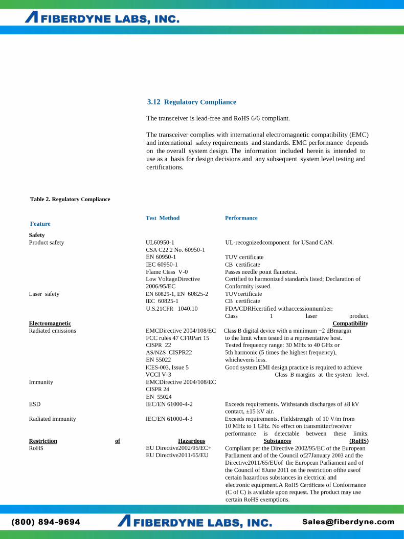
3.12 Regulatory Compliance
The transceiver is lead-free and RoHS 6/6 compliant.
The transceiver complies with international electromagnetic compatibility (EMC)
and international safety requirements and standards. EMC performance depends
on the overall system design. The information included herein is intended to
use as a basis for design decisions and any subsequent system level testing and
certifications.
Table 2. Regulatory Compliance
Feature Test Method Performance
Safety
Product safety UL60950-1 UL-recognizedcomponent for USand CAN.
CSA C22.2 No. 60950-1
EN 60950-1 TUV certificate
IEC 60950-1 CB certificate
Flame Class V-0
Low VoltageDirective
2006/95/EC
Passes needle point flametest.
Certified to harmonized standards listed; Declaration of
Conformity issued.
Laser safety EN 60825-1, EN 60825-2
IEC 60825-1
TUVcertificate
CB certificate
U.S.21CFR 1040.10 FDA/CDRHcertified withaccessionnumber;
Class 1 laser product.
Electromagnetic Compatibility
Radiated emissions EMCDirective 2004/108/EC Class B digital device with a minimum −2 dBmargin
FCC rules 47 CFRPart 15
CISPR 22
AS/NZS CISPR22
EN 55022
to the limit when tested in a representative host.
Tested frequency range: 30 MHz to 40 GHz or
5th harmonic (5 times the highest frequency),
whicheveris less.
ICES-003, Issue 5
VCCI V-3
Good system EMI design practice is required to achieve
Class B margins at the system level.
Immunity EMCDirective 2004/108/EC
CISPR 24
EN 55024
ESD IEC/EN 61000-4-2 Exceeds requirements. Withstands discharges of ±8 kV
contact, ±15 kV air.
Radiated immunity IEC/EN 61000-4-3 Exceeds requirements. Fieldstrength of 10 V/m from
10 MHz to 1 GHz. No effect on transmitter/receiver
performance is detectable between these limits.
Restriction
RoHS
of Hazardous
EU Directive2002/95/EC+
EU Directive2011/65/EU
Substances (RoHS)
Compliant per the Directive 2002/95/EC of the European Parliament and of the Council of27January 2003 and the
Directive2011/65/EUof the European Parliament and of
the Council of 8June 2011 on the restriction ofthe useof
certain hazardous substances in electrical and
electronic equipment.A RoHS Certificate of Conformance
(C of C) is available upon request. The product may use
certain RoHS exemptions.

3.13 Module Outline

SFP+ C-BAND TUNABLE DWDM OPTICAL TRANSCEIvER
Note: It is recommended that the connector plug remain on whenever the trans-
ceiver optical fiber connector is not inserted.
Recommended Cleaning and De-greasing Chemicals
FIBERDYNE recommends the use of methyl, isopropyl and isobutyl alcohols for
cleaning.
This product is not designed for aqueous wash.
Housing
The transceiver housing is made from zinc.
3.14 Connectors
Fiber
Themodule has a duplex LC receptacleconnector.
Do not use halogenated hydrocarbons (e.g. trichloroethane, ketones such as acetone,
chloroform, ethyl acetate, MEK, methylene chloride, methylene dichloride, phenol,
N-methylpyrolldone).
Electrical
The electrical connector is the 20-way, two-row PCB edge connector. Customer
connector is Tyco/AMP Part No. 188247 or equivalent.
The transceiver is supplied with an LC duplex receptacle. The connector plug
supplied protects the connector during standard manufacturing processes and
handling by preventing contamination from dust, aqueous solutions, body oils, or
airborne particles.
Connector Covers
4.1 Package and Handling Instructions
• Section 4.1
• Section 4.2
• Section 4.3
Packing and Handling Instructions
ElectrostaticDischarge (ESD)
Laser Safety
Other information related to the transceiver includes:
Related
Information
Section 4 :

Caution
Use of controls or adjustments or performance of procedures other than these
specified in this product data sheet may result in hazardous radiation exposure.
Tampering with this laser product or operating this product outside the limits of
this specification may be considered an “act of manufacturing” and may require
recertification of the modified product.
Viewing the laser output with certain opticalinstruments (for example, eye loupes,
magnifiers,microscopes) within a distance of 100mm may pose an eye hazard.
Ordering Information
Model Number Data Wavelength Material Fib Distance D
FDN-SFP-10G-TD-40DXX 8/10g Tunable Wavelength DWDM+PIN SM 40km
FDN-SFP-10G-TD-80DXX 8/10g Tunable Wavelength DWDM+APD SM 80km
Operating this product in a manner inconsistent with intended usageand specifi-
cations may result in hazardous radiation exposure.
The transceiver complies with 21 CFR 1040.10 except for deviations pursuant to
Laser Notice No. 50 dated June 24,2007.
The transceiver is certified as a Class 1 laser product per international standard
IEC 60825-1:2007 2nd edition and is considered non-hazardous when operated
within the limits of this specification.
4.3 Laser Safety
In most applications, the optical connector will protrude through the system chassis
and be subjected to the same ESD environment as the system. Once properly
installed in the system, this transceiver should meet and exceed common ESD
testing practices and fulfill systemESD requirements.
Typical of optical transceivers, this module’s receiver contains a highly sensitive
optical detector and amplifier which may become temporarily saturated during
an ESD strike. This could result in a short burst of bit errors. Such an event might
require that the application re-acquire synchronization at the higher layers (for
example,viaa serializer/deserializer chip).
Test and Operation
Normal ESD precautions are required during the handling of this module. This
transceiver is shipped in ESD protective packaging. It should be removed from
the packaging and otherwise handled in an ESD protected environment utilizing
standard grounded benches, floor mats, and wrist straps.
Handling
4.2 Electrostatic Discharge (ESD)