session t1a microelectronic engineering education for...
TRANSCRIPT
Session T1A
/10/$25.00 ©2010 IEEE October 27 - 30, 2010, Washington, DC 40th ASEE/IEEE Frontiers in Education Conference T1A-1
Microelectronic Engineering Education for Emerging Technologies
Santosh Kurinec, Michael Jackson, Davide Mariotti, Surendra Gupta, Sean Rommel, Dale Ewbank, Karl Hirschman, Robert Pearson, and Lynn Fuller
Rochester Institute of Technology [email protected], [email protected]; [email protected], [email protected], [email protected],
[email protected], [email protected], [email protected], [email protected]
Abstract- The Department of Microelectronic Engineering at Rochester Institute of Technology received NSF Department Level Reform (DLR) planning and implementation grants in 2003-04 and 2005-10, respectively. The primary mission of these efforts was to evaluate and develop educational initiatives towards nanotechnology aligned with recommendations from the institution of National Nanotechnology Initiatives published by the US Government in 2000. The Department proposed to take this opportunity further and guide its curriculum toward new frontiers in nanotechnology and micro-electro-mechanical systems (MEMs). Advances in semiconductor technology have resulted in micro/nanofabrication techniques being employed in MEMs, chemical & bio sensors, and in energy harvesting devices and systems. The technology has evolved through aggressive process control and scalability characterized by Moore’s Law. The result has been emergence of a multifunctional “More than Moore” regime that is increasingly multidisciplinary in nature. Under this effort, new courses and curricula in Microelectronics and Nanofabrication providing access to state-of-the art semiconductor fabrication facilities to students from different science and engineering programs have been formulated. Index Terms – Department Level Reform, Nanotechnology Education, Nanofabrication, MEMs
INTRODUCTION
Every major world economy has identified the areas - nanotechnology, microelectronics, photonics, new materials, alternative energy, and biotech that will drive innovation and economic growth. The most fundamental driver is modernization of education in these areas. RIT started the nation’s first Bachelor of Science program in Microelectronic Engineering in 1982 to drive the PC revolution that had just begun. The 196 quarter credit BS program combines the basic electrical engineering curriculum with optics, lithography, semiconductor processing, materials science, design, and manufacturing. The program requires 15 months of co-op experience. The
Co-op commences after the second year, and students alternate school with paid employment in the semiconductor industry. The program has constantly advanced its integrated circuit fabrication laboratory in order to graduate students with state- of-the-art knowledge, who become immediate and efficient contributors to their company or graduate program. Today, this facility serves as a key resource for research in semiconductor devices, processes, MEMS, nanotechnology, and Microsystems [1].
The Engineering Education Center (EEC) division of the National Science Foundation (NSF) established the Department-Level Reform (DLR) initiative for Undergraduate Engineering Education programs in 2002 [2,3]. The DLR solicitation was an opportunity to compete for grants to enable departments to 1) reformulate, streamline and update engineering degree programs; 2) develop novel curricula in newly developing areas for meeting the emerging workforce and educational needs of U.S. industry, and 3) integrate research and teaching with service learning. Grants were available for both planning and implementation efforts. The Department of Microelectronic Engineering received a planning grant in 2003 and an implementation grant in 2005 to take its curriculum to emerging frontiers of nanotechnology and MEMs. The highlights of each of these grants are described as follows.
I. DLR Planning Initiative
A one-year DLR planning grant entitled “Undergraduate Co-op Based Concentration Curriculum in MEMs and Nanotechnology” was to define and develop new undergraduate nanotechnology and MEMS concentration courses. A multidisciplinary planning team was assembled. The uniqueness of this proposal was a direct collaboration between the College of Engineering and the RIT Office of Cooperative Education and Career Services. The team collected information from industry leaders and employers. With the existing BS Microelectronic Engineering curriculum as a foundation, the team sought to assemble multidisciplinary curricula that best met the educational needs of students and the workforce needs of employers in the emerging fields of nanotechnology and MEMS [4]. At
/10/$25.00 ©2010 IEEE 40th ASEE/IEEE Frontiers in Education Conference
the same time RIT instituted the nation’s first PhD program in Microsystems Engineering building upon the strength of Microelectronic Engineering undergraduate program and its cleanroom IC fabrication facility. undergraduate program became necessary for feeding students to the PhD program.
II. DLR Implementation Initiative
Following the successful execution of the planning grant, the department of Microelectronic Engineeringproposal for an implementation grant in 2005. The main thrusts were (1) crafting a five course elective sequence within the existing curriculum by eliminating legacy material and course consolidation; (2) offering a Microelectronics and Nanofabrication access to state-of-the art semiconductor fabrication facilities to students from other science and engineering programs; (3) developing a concentration program in nanotechnology and MEMS; (4) delivering outreach programs for attra larger and more diverse population to meet workforce needs for the nation’s future high tech industry; (5) enhancing student learning through co-op and service. The proposal was endorsed by leading industries and consortia that included ASML, IBM, Intel, Micron, National Semiconductors, Texas Instruments, SemicResearch Corporation and SEMATECH.
APPROACH
The planning phase began with organization of a on Nanotechnology and Microelectromechanical Systems (MEMS) Education. The objective of the workshop was to raise the awareness among educational institutions, KUniversity, and in industry of the emergence of technologies, such as nanotechnology and MEMS. The workshop was attended by over 70 peopleand industry, including 13 participants from and High schools. After exhaustive deliberations following the one year planning period, the following needs were identified:
• Development of flexible curricula in engineering and science that allowed courses in nanotechnology and MEMs.
• Development of hands-on laboratory based outreach for K-12 Teachers in practical nanotechnology
• Innovation of relevant service learning program for microelectronic engineering students
These findings were communicated to Dean of the College of Engineering and the Provost for Academic Affairs. An institute wide initiative was proposed and subsequently implemented [5]. Thechange was that all undergraduate degree programs must
October 27ASEE/IEEE Frontiers in Education Conference
T1A-2
the same time RIT instituted the nation’s first PhD program in Microsystems Engineering building upon the strength of
lectronic Engineering undergraduate program and its Reformulation of
necessary for feeding
the planning grant, the department of Microelectronic Engineering submitted a proposal for an implementation grant in 2005. The main thrusts were (1) crafting a five course elective sequence within the existing curriculum by eliminating legacy material and course consolidation; (2) offering a
brication minor promoting the art semiconductor fabrication facilities
to students from other science and engineering programs; (3) developing a concentration program in nanotechnology and MEMS; (4) delivering outreach programs for attracting a larger and more diverse population to meet workforce needs for the nation’s future high tech industry; (5)
op and service. The leading industries and consortia
, Intel, Micron, National Semiconductors, Texas Instruments, Semiconductor Research Corporation and SEMATECH.
The planning phase began with organization of a workshop on Nanotechnology and Microelectromechanical Systems
tive of the workshop was to raise the awareness among educational institutions, K-12 to
of the emergence of disruptive anotechnology and MEMS. The
workshop was attended by over 70 people from academia , including 13 participants from local Middle
After exhaustive deliberations following following needs were
Development of flexible curricula in engineering urses in nanotechnology
on laboratory based 12 Teachers in practical
Innovation of relevant service learning program for microelectronic engineering students
communicated to the faculty, the Dean of the College of Engineering and the Provost for
institute wide initiative was proposed ]. The key feature of this
ate degree programs must
contain at least 12 quarter credits of entirely open electiveswithin the degree program’s distribution
MINOR PROGRAMS
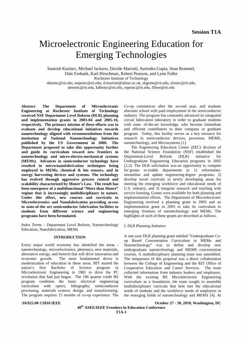
These five free elective courses provided opportunities for creation of a number of new minor programs withininstitute. This allowed student to attain multidisciplinary education. The BS Microelectronic Engineering curriculumthat had only two professional electivesby course restructuring and consolidation three free electives. These three electives combined with two professional electives allowed students to take minor programs as depicted in Figure 1.
FIGURE
CREATION OF FIVE ELECTIVE COURSES TO
PROGRAMS
A new minor program “
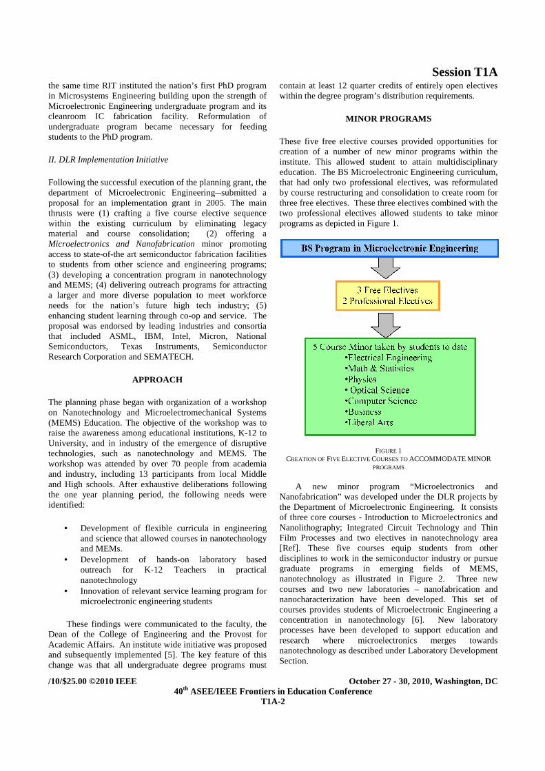
Nanofabrication” was developed under the DLR projects the Department of Microelectronic Engineering. It of three core courses - IntrodNanolithography; Integrated CircuitFilm Processes and two electives in nanotechnology area [Ref]. These five courses disciplines to work in the semiconductor industry graduate programs in emerging fields of MEMS, nanotechnology as illustrated in Figure 2. courses and two new laboratories nanocharacterization have been developedcourses provides students of Microelectronic Engineering a concentration in nanotechnologyprocesses have been developed to support education and research where microelectronics merges towards nanotechnology as described under Laboratory Development Section.
Session T1A
27 - 30, 2010, Washington, DC
12 quarter credits of entirely open electives distribution requirements.
MINOR PROGRAMS
These five free elective courses provided opportunities for creation of a number of new minor programs within the institute. This allowed student to attain multidisciplinary
The BS Microelectronic Engineering curriculum, that had only two professional electives, was reformulated by course restructuring and consolidation to create room for
lectives. These three electives combined with the two professional electives allowed students to take minor programs as depicted in Figure 1.
IGURE 1 OURSES TO ACCOMMODATE MINOR
PROGRAMS
A new minor program “Microelectronics and developed under the DLR projects by
the Department of Microelectronic Engineering. It consists Introduction to Microelectronics and
Nanolithography; Integrated Circuit Technology and Thin Film Processes and two electives in nanotechnology area
These five courses equip students from other disciplines to work in the semiconductor industry or pursue graduate programs in emerging fields of MEMS,
ustrated in Figure 2. Three new two new laboratories – nanofabrication and
have been developed. This set of students of Microelectronic Engineering a
concentration in nanotechnology [6]. New laboratory ocesses have been developed to support education and
research where microelectronics merges towards as described under Laboratory Development
/10/$25.00 ©2010 IEEE 40th ASEE/IEEE Frontiers in Education Conference
FIGURE 2
MOTIVATION FOR MINOR PROGRAM IN MICROELECTRONICS AND
NANOFABRICATION
I. Courses Restructured
The following courses were restructured:Electromagnetic Fields (Undergraduate)A single course in Electromagnetic (EM) Fields out of the two existing courses. Extensive deliberations were done to ensure that students get a sufficient foundation in EM field fundamentals for applications involvingsemiconductor devices, optics and processing courses. An online precourse tutorial was prepared that students could access prior to taking the new EM Fields course to review the necessary calculus. Reformatting the EM course helpcreate room for a free elective necessary for enablminor program within the BS program. Quantum and Solid Sate Fundamentals for Nanostructures (Graduate) Typically quantum mechanics and solid state ptaught as separate courses in most physics and engineering curricula. It is often not possible for students to take both of these courses in their BS (EE or MicroE) programs. Electrical engineers entering nanoscale device technologies need to know basic components coming from both of these courses. This new modified course describes the key elements of quantum mechanics and solid state physics that are necessary in understanding the modern semiconductor devices. Quantum mechanical topics includeSchrodinger equation solution for potential wells and barriers, subsequently applied to tunneling and carrier confinement. Solid state topics include crystal structures, direct and reciprocal lattices, effective mass theory, energymomentum relations in direct and in
October 27ASEE/IEEE Frontiers in Education Conference
T1A-3
ICROELECTRONICS AND
The following courses were restructured: Electromagnetic Fields (Undergraduate)
Electromagnetic (EM) Fields was crafted Extensive deliberations were
sufficient foundation in eld fundamentals for applications involving
ocessing courses. An course tutorial was prepared that students could
taking the new EM Fields course to review Reformatting the EM course help
ree elective necessary for enabling a
Quantum and Solid Sate Fundamentals for
solid state physics are taught as separate courses in most physics and engineering curricula. It is often not possible for students to take both of these courses in their BS (EE or MicroE) programs. Electrical engineers entering nanoscale device technologies
g from both of these This new modified course describes the key
elements of quantum mechanics and solid state physics that are necessary in understanding the modern semiconductor devices. Quantum mechanical topics include solution of Schrodinger equation solution for potential wells and barriers, subsequently applied to tunneling and carrier confinement. Solid state topics include crystal structures,
effective mass theory, energy-lations in direct and indirect band gap
semiconductors, and statistical physics appliedsemiconductors. Nanoscale CMOS and Beyond (Graduate)This course encompasses an inpractice of scaling-driven CMOS front processing. The course discusses International Technology Roadmap for Semiconductors (ITRS)students to the next generation of nanometerwith device concepts that include quantum mechanical phenomena such as channel confinement and dopant fluctuations. Front end processing includes super steep retrograde wells, high-k gate insultra shallow source/ drains. Back end topics include interconnect modeling and delay, land copper damanscence processessubstrates such as strained silicon, SiGe, Ge, IIIgraphene are also discussed. Microelectromechanical Systems This course provides an opportunity for students to become familiar with the technology and applications of one of the fastest growing areas in the semiconductor business. MEMS represent the inchips with microsensors, probs, lasers, and actuators. Topics include basic principles of MEMS and fabrication methodologies. The accompanying laboratory will carry out design and fabrication of MEMS structures/devices using microfabrication techniques. accompanied by MEMS design courses offered by the electrical engineering department for students interested in Microsystems concentration in their graduate II. New Courses Developed The following new courses were developed by the Department of Microelectronic Engineering during the DLR funding period: Introduction to nanotechnology (Undergraduate) Nanotechnology aims to control properties at atomic or molecular level or to realize components witdimensions below 100nm. It enables new functionality, improved performance, higher density of information storage and processing within and around advanced semiconductor technology platforms. This course nano properties based on chemimaterials and their interface with solid state devices. course provides the option to students to be involved in small experimental projects. Most students have opted for the experimental projects. The course also included 4of demonstration related to characterization tools and in collaboration with multidisciplinary faculty. Nanofabrication (Undergraduate)This course covers the different approaches for creating nanostructures and nanodevices, including “top down” an
Session T1A
27 - 30, 2010, Washington, DC
statistical physics applied to carriers in
Nanoscale CMOS and Beyond (Graduate) This course encompasses an in-depth study of principles and
driven CMOS front and back end processing. The course discusses International Technology
Semiconductors (ITRS) [7] and exposes students to the next generation of nanometer-scale CMOS with device concepts that include quantum mechanical phenomena such as channel confinement and dopant fluctuations. Front end processing includes super steep
k gate insulators, metal gates, and ultra shallow source/ drains. Back end topics include
onnect modeling and delay, low permittivity dielectric processes. The use of novel
ned silicon, SiGe, Ge, III-V and
Microelectromechanical Systems provides an opportunity for students to become
familiar with the technology and applications of MEMS - one of the fastest growing areas in the semiconductor
the integration of microelectronic chips with microsensors, probs, lasers, and actuators. Topics include basic principles of MEMS and fabrication methodologies. The accompanying laboratory will carry out design and fabrication of MEMS structures/devices using
crofabrication techniques. This course is also accompanied by MEMS design courses offered by the electrical engineering department for students interested in Microsystems concentration in their graduate study [8].
new courses were developed by the Department of Microelectronic Engineering during the DLR
Introduction to nanotechnology (Undergraduate) Nanotechnology aims to control properties at atomic or molecular level or to realize components with critical dimensions below 100nm. It enables new functionality, improved performance, higher density of information storage and processing within and around advanced
ogy platforms. This course introduces nano properties based on chemical and physical nature of materials and their interface with solid state devices. The
the option to students to be involved in small experimental projects. Most students have opted for the experimental projects. The course also included 4 hours of demonstration related to characterization tools and in collaboration with multidisciplinary faculty.
n (Undergraduate) This course covers the different approaches for creating nanostructures and nanodevices, including “top down” and
Session T1A
/10/$25.00 ©2010 IEEE October 27 - 30, 2010, Washington, DC 40th ASEE/IEEE Frontiers in Education Conference T1A-4
“bottom up” techniques, with a discussion of the capabilities and limits of each. Students learn the fundamental physics, chemistry and material science of nanofabrication, as well as the practical aspects of the creative process of building functional structures at the nanoscale. Topics covered in the course include: advanced lithography technologies, including photon, electron, ion and atom, scanning probe, “soft lithography” and nanoimprinting; pattern transfer; self-assembly; process integration; characterization; and applications. This course is developed with laboratory sessions. Micro/Nano Characterization (Graduate) This technical elective with weekly lab component focuses on tools and techniques for micro- and nano-characterization of materials, surfaces and thin films. The course covers the principles and applications of two characterization techniques: x ray diffraction and scanning probe microscopy (acquired through this grant). Students learn the physics of interaction processes used for characterization, quantification and interpretation of collected signals, and fundamental detection limits for each technique. Photovoltaics Science and Engineering (Graduate/Senior) This course focuses on the principle and engineering fundamentals of photovoltaic (PV) energy conversion. The course covers modern silicon PV devices, including the basic physics, ideal and non-ideal models, device parameters and design, and device fabrication. The course discusses crystalline, multi-crystalline, amorphous devices thin films solar cells and their manufacturing. Students are made familiar on how basic semiconductor processes are employed in solar cells manufacturing. The course further introduces third generation advanced photovoltaic concepts including compound semiconductors, spectral conversion, and organic and polymeric devices. PV applications, environmental and economic issues will also be discussed [9]. Memory Systems (Graduate) The course targets the overlapping areas of device physics and design, advanced processes, electrical characterization and circuit architecture as it applies to modern memory systems. While there are no specific set of pre-requisite courses, students should be willing to work on problems involving the previously mentioned topics. Course work will trace the design, development, fabrication, packaging and testing of SRAM, DRAM and Flash Memory, and then branch off into MRAM, FRAM and PRAM technology. The course wraps up with an exploration of future memory system candidates such as quantum, molecular and optical memory systems. SiGe and SOI Devices and Technologies (Graduate) This course introduces students to the fundamentals of SiGe and Silicon on Insulator (SOI) devices and fabrication
technologies. The course will first discuss the band structure of the SiGe material system, and how its properties of band structure and enhanced mobility may be utilized to improve traditional Si devices. Basic heterojunction theory is introduced to students. Some specific applications that are introduced include heterojunction bipolar transistors (HBTs), SiGe-channel MOS devices, and high-electron mobility transistors (HEMTs). Fabrication technologies for realizing SOI substrates that include SIMOX and SMART CUTTM technologies are described.
LABORATORY DEVELOPMENT
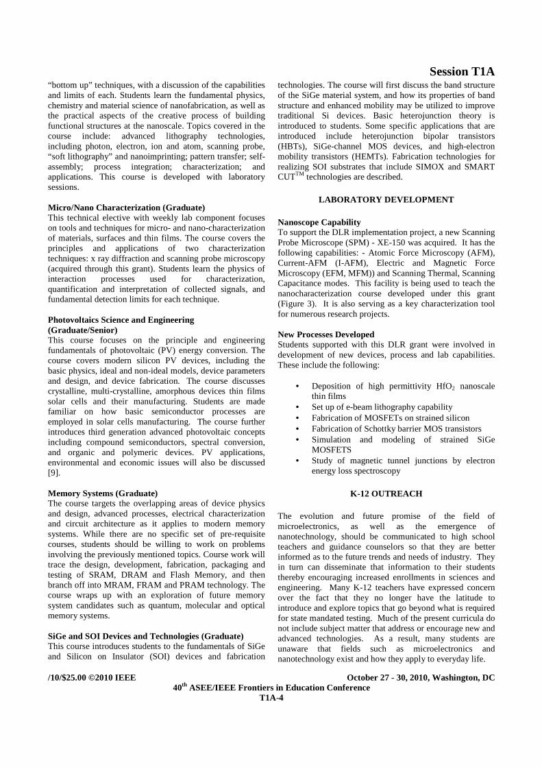
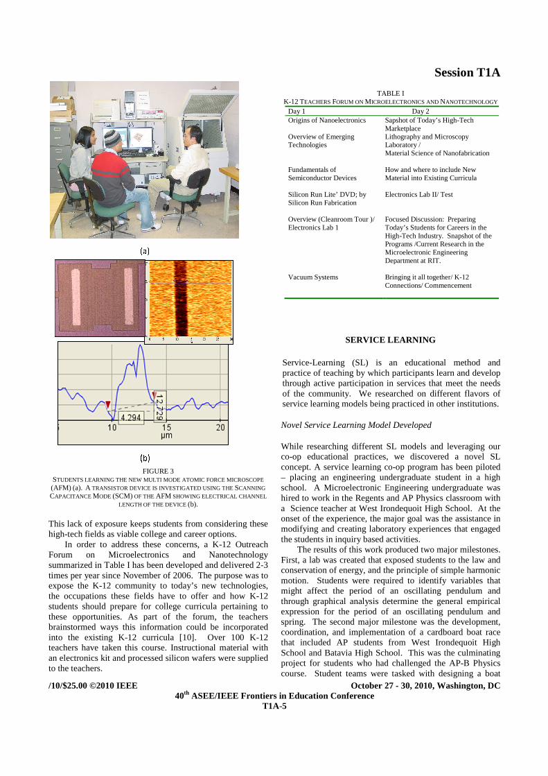
Nanoscope Capability To support the DLR implementation project, a new Scanning Probe Microscope (SPM) - XE-150 was acquired. It has the following capabilities: - Atomic Force Microscopy (AFM), Current-AFM (I-AFM), Electric and Magnetic Force Microscopy (EFM, MFM)) and Scanning Thermal, Scanning Capacitance modes. This facility is being used to teach the nanocharacterization course developed under this grant (Figure 3). It is also serving as a key characterization tool for numerous research projects. New Processes Developed Students supported with this DLR grant were involved in development of new devices, process and lab capabilities. These include the following:
• Deposition of high permittivity HfO2 nanoscale thin films
• Set up of e-beam lithography capability • Fabrication of MOSFETs on strained silicon • Fabrication of Schottky barrier MOS transistors • Simulation and modeling of strained SiGe
MOSFETS • Study of magnetic tunnel junctions by electron
energy loss spectroscopy
K-12 OUTREACH
The evolution and future promise of the field of microelectronics, as well as the emergence of nanotechnology, should be communicated to high school teachers and guidance counselors so that they are better informed as to the future trends and needs of industry. They in turn can disseminate that information to their students thereby encouraging increased enrollments in sciences and engineering. Many K-12 teachers have expressed concern over the fact that they no longer have the latitude to introduce and explore topics that go beyond what is required for state mandated testing. Much of the present curricula do not include subject matter that address or encourage new and advanced technologies. As a result, many students are unaware that fields such as microelectronics and nanotechnology exist and how they apply to everyday life.
/10/$25.00 ©2010 IEEE 40th ASEE/IEEE Frontiers in Education Conference
FIGURE 3 STUDENTS LEARNING THE NEW MULTI MODE ATOMI
(AFM) (a). A TRANSISTOR DEVICE IS INVESTIGATED USING T
CAPACITANCE MODE (SCM) OF THE AFM SHOWING ELECTRIC
LENGTH OF THE DEVICE (b This lack of exposure keeps students from considering these high-tech fields as viable college and career options.
In order to address these concerns, aForum on Microelectronics and Nanotechnology summarized in Table I has been developed and delivered 2times per year since November of 2006. expose the K-12 community to today’s new technologies, the occupations these fields have to offer and how Kstudents should prepare for college curricula pertaining to these opportunities. As part of the forum, the teachers brainstormed ways this information could be incorporainto the existing K-12 curricula [10]teachers have taken this course. Instructional material with an electronics kit and processed silicon wafers were supplied to the teachers.
October 27ASEE/IEEE Frontiers in Education Conference
T1A-5
NEW MULTI MODE ATOMIC FORCE MICROSCOPE
INVESTIGATED USING THE SCANNING
SHOWING ELECTRICAL CHANNEL
b).
keeps students from considering these tech fields as viable college and career options.
In order to address these concerns, a K-12 Outreach Forum on Microelectronics and Nanotechnology
has been developed and delivered 2-3 times per year since November of 2006. The purpose was to
12 community to today’s new technologies, the occupations these fields have to offer and how K-12
curricula pertaining to these opportunities. As part of the forum, the teachers brainstormed ways this information could be incorporated
[10]. Over 100 K-12 Instructional material with
electronics kit and processed silicon wafers were supplied
TABLE I
K-12 TEACHERS FORUM ON M ICROELECTRONICS AND
Day 1 Origins of Nanoelectronics Overview of Emerging Technologies Fundamentals of Semiconductor Devices Silicon Run Lite’ DVD; by Silicon Run Fabrication Overview (Cleanroom Tour )/ Electronics Lab 1 Vacuum Systems
Sapshot of Today’s HighMarketplaceLithography and Microscopy Laboratory /Material Science of How and where to inclMaterial into Existing C Electronics Lab II/ Test Focused Discussion: Preparing Today’s Students for Careers in the HighPrograms /Current RMicroelectDepartment at RIT. Bringing it all together/ KConnections/ Commencement
SERVICE LEARNING
Service-Learning (SL) is an educational method and practice of teaching by which participants learn and develop through active participation in services that meet the needs of the community. We researched on different flavors of service learning models being practiced in other institutions.
Novel Service Learning Model Developed
While researching different SL models and leveraging our co-op educational practices, we discovconcept. A service learning co– placing an engineering undergraduate student in a high school. A Microelectronic Engineering hired to work in the Regents and AP Physics classroom a Science teacher at West Irondequoit High School. At the onset of the experience, the major goal was the assistance in modifying and creating laboratory experiences that engaged the students in inquiry based activities.
The results of this work produced two major milestones. First, a lab was created that exposed students to the law and conservation of energy, and the principle of simple harmonic motion. Students were required to identify variables that might affect the period of an oscillating pendulum and through graphical analysis determine the general empirical expression for the period of an oscillating pendulum and spring. The second major milestone was the development, coordination, and implementation of a cardboard boat race that included AP students from West Irondequoit High School and Batavia High School. This was the culminatproject for students who had challenged the APcourse. Student teams were tasked with designing a boat
Session T1A
27 - 30, 2010, Washington, DC
TABLE I ICROELECTRONICS AND NANOTECHNOLOGY
Day 2 Sapshot of Today’s High-Tech Marketplace Lithography and Microscopy Laboratory / Material Science of Nanofabrication How and where to include New Material into Existing Curricula Electronics Lab II/ Test Focused Discussion: Preparing Today’s Students for Careers in the High-Tech Industry. Snapshot of the Programs /Current Research in the Microelectronic Engineering Department at RIT. Bringing it all together/ K-12 Connections/ Commencement
SERVICE LEARNING
Learning (SL) is an educational method and practice of teaching by which participants learn and develop through active participation in services that meet the needs
We researched on different flavors of ing practiced in other institutions.
Novel Service Learning Model Developed
While researching different SL models and leveraging our op educational practices, we discovered a novel SL
service learning co-op program has been piloted ing an engineering undergraduate student in a high
Microelectronic Engineering undergraduate was hired to work in the Regents and AP Physics classroom with
Science teacher at West Irondequoit High School. At the major goal was the assistance in
modifying and creating laboratory experiences that engaged the students in inquiry based activities.
The results of this work produced two major milestones. First, a lab was created that exposed students to the law and onservation of energy, and the principle of simple harmonic
motion. Students were required to identify variables that might affect the period of an oscillating pendulum and through graphical analysis determine the general empirical
od of an oscillating pendulum and spring. The second major milestone was the development, coordination, and implementation of a cardboard boat race that included AP students from West Irondequoit High School and Batavia High School. This was the culminating project for students who had challenged the AP-B Physics course. Student teams were tasked with designing a boat
Session T1A
/10/$25.00 ©2010 IEEE October 27 - 30, 2010, Washington, DC 40th ASEE/IEEE Frontiers in Education Conference T1A-6
made solely from cardboard and duct tape that would carry two students across a school swimming pool. Understanding concepts in structural design and buoyancy were critical to this project. It provided faster response to student questions and certainly made for a stronger learning environment in teacher’s classroom. The response to this program during the first quarter was positive from both a student perspective as well as a teacher perspective. The ability to have someone with the necessary technical knowledge to help strengthen the lab component of a course is invaluable especially when time is very limited for individually work on. The access to a second person in the classroom to assist students working in small groups provides faster response time to student questions as well as provides multiple approaches to problem solving which helps student learning.
SUMMARY
The rapid advancements in the semiconductor industry have brought the technology into new realms of nanotechnology and micro/nano systems engineering. With the support provided by the NSF DLR program and RIT Provost’s vision, a major curricular restructuring has been made possible in microelectronic engineering program at RIT. The efforts have been so far successful in creating modern and novel curricula, outreach, and service learning opportunities. These initiatives are extremely critical in producing the next generation of engineers to stay ahead in innovations and be globally competitive.
ACKNOWLEDGMENT
The authors gratefully acknowledge the support provided by the National Science Foundation for the DLR planning grant # EEC-0342703 and implementation grant # EEC-530575.
REFERENCES [1] Kurinec S.K, Fuller L. F, Smith B.W, Lane R.L, , Hirschman K.D, Jackson M.A, et al, “25 Years of Microelectronic Engineering Education”, 16th Biennial University Government Industry Microelectronics Symposium, San Jose State University, San Jose, CA, June 2006, p.23 [2] Division of Engineering Education and Centers National Science Foundation; www.nsf.gov [3] Shipp S, Mitchell N, Lal B, “ Portfolio Evaluation of the National Science Foundation’s Grants Program for the Department-level Reform of Undergraduate Engineering Education,”, IDA, Science and Technology Policy Institute, IDA Document, D-3724 [4] Kurinec S.K, Fuller L.F, Wiegand M, Arquette M, “Undergraduate Co-op Based Concentration Curriculum in MEMs and Nanotechnology” American Society for Engineering Education, St. Lawrence Section, Engineering on the Edge: Engineering in the New Century, Binghamton University, April 8-9, 2005. [5] Kurinec S. K, Jackson M. A, Mariotti D, Gupta S, Rommel S, et al, “Role of Institutional Support for NSF Department Level Reform Grants”, American Society for Engineering Education, St. Lawrence Section, Rochester, New York, March 2010
[6] Mariotti D, Jackson M, Lewis E, Schulte T, Kurinec S, “Nanotechnology in Education: Top-down and Bottom-up Approach”, “ iNEER Innovations 2008 Special Volume, Innovations 2008, World Innovations in Engineering Education and Research (2008) 261 [7] International Technology Roadmap for Semiconductors, www.itrs.net [8] Pearson R. E, Fuller L. F, Puchades I., “MEMS Fabrication Course for Pressure Sensors, Flow Sensors, Fluidic Channels and Micro-Pumps”, Proc. 17th University Government Industry Microelectronics Symposium, Louisville, Kentucky, July 2008 [9] Kurinec S. K, Jackson M. A, “A New Course on Photovoltaics for Engineering and Science Curricula” American Society for Engineering Education, St. Lawrence Section, Rochester, New York, March 2010 [10] Jackson M.A, Schulte T, Kane N, Lewis E, Gupta S.K, and Kurinec S.K, , Microelectronic Engineering and Nanotechnology Education for Undergraduates and Pre-College Students through Curriculum Reform and Outreach Activities, American Society for Engineering Education, Pittsburgh, June 2008
AUTHOR INFORMATION
Santosh K. Kurinec, Principal Investigator and Department Head of Microelectronic Engineering 2001-2009, Professor, Rochester Institute of Technology, [email protected] Michael A. Jackson, Outreach Program Director, Associate Professor of Microelectronic Engineering, Rochester Institute of Technology, [email protected] Davide Mariotti, Visiting Assistant Professor, Microelectronic Engineering, Rochester Institute of Technology, Currently at University of Ulster, UK, [email protected] Surendra Gupta, Professor, Mechanical Engineering, Director, Advanced Materials Characterization Laboratory, Rochester Institute of Technology, [email protected] Sean Rommel, Associate Professor of Microelectronic Engineering, Tunnel Devices and E-Beam Lithography Director, Rochester Institute of Technology , [email protected] Robert Pearson, Associate Professor and Program Director of Microelectronic Engineering, Rochester Institute of Technology, [email protected] Dale Ewbank, Assistant Professor, Design of Experiments and Microlithography Professor, Rochester Institute of Technology, [email protected] Karl D Hirschman , Associate Professor and Director, Semiconductor and Microsystems Fabrication Laboratory, Rochester Institute of Technology, [email protected] Lynn F Fuller , Professor and Founder Department Head of Microelectronic Engineering, Rochester Institute of Technology,[email protected]