series for design engineers - index-of.co.ukindex-of.co.uk/tutorials-2/power supply cookbook -...
TRANSCRIPT


Brown Power Supply Cookbook, Second EditionDostál Operational Amplifiers, Second EditionDye Radio Frequency Transistors: Principles and Practical Applications, Second
EditionGates Energy Products Rechargeable Batteries Applications HandbookHickman Electronic Circuits, Systems and Standards: The Best of EDNMarston Newnes Electronic Circuits Pocket BookMarston Integrated Circuit and Waveform Generator HandbookMarston Diode, Transistor and FET Circuits ManualPease Troubleshooting Analog CircuitsSinclair Passive ComponentsWilliams Analog Circuit Design: Art, Science and Personalities
Series for Design Engineers

Power Supply
CookbookSecond Edition
Marty Brown
Boston Oxford Johannesburg Melbourne New Delhi

Newnes is an imprint of Butterworth–Heinemann.Copyright © 2001 by Butterworth–HeinemannA member of the Reed Elsevier groupAll rights reserved.
No part of this publication may be reproduced, stored in a retrieval system, ortransmitted in any form or by any means, electronic, mechanical, photocopying,recording, or otherwise, without the prior written permission of the publisher.
Recognizing the importance of preserving what has been written,Butterworth–Heinemann prints its books on acid-free paper whenever possible.Butterworth–Heinemann supports the efforts of American Forests and the GlobalReLeaf program in its campaign for the betterment of trees, forests, and ourenvironment.
Library of Congress Cataloging-in-Publication Data
Brown, Marty.Power supply cookbook / Marty Brown.—2nd ed.
p. cm.Includes bibliographical references and index.ISBN 0-7506-7329-X1. Electric power supplies to apparatus—Design and construction.
2. Power electronics. 3. Electronic apparatus and appliances—powersupply. I. Title.TK7868.P6 B76 2001621.381¢044—dc21
00-050054
British Library Cataloguing-in-Publication Data
A catalogue record for this book is available from the British Library.
The publisher offers special discounts on bulk orders of this book.For information, please contact:Manager of Special SalesButterworth–Heinemann225 Wildwood AvenueWoburn, MA 01801-2041Tel: 781-904-2500Fax: 781-904-2620
For information on all Newnes publications available, contact our World Wide Webhome page at: http://www.newnespress.com
10 9 8 7 6 5 4 3 2 1
Printed in the United States of America

Power Supply CookbookSecond Edition

Contents
Preface ix
Introduction xi
1. The Role of the Power Supply within the System and the Design Program1.1 Getting Started. This Journey Starts with the First Question 11.2 Power System Organization 21.3 Selecting the Appropriate Power Supply Technology 31.4 Developing the Power System Design Specification 51.5 A Generalized Approach to Power Supplies: Introducing the
Building-block Approach to Power Supply Design 81.6 A Comment about Power Supply Design Software 91.7 Basic Test Equipment Needed 9
2. An Introduction to the Linear Regulator2.1 Basic Linear Regulator Operation 112.2 General Linear Regulator Considerations 122.3 Linear Power Supply Design Examples 142.3.1 Elementary Discrete Linear Regulator Designs 152.3.2 Basic 3-Terminal Regulator Designs 152.3.3 Floating Linear Regulators 18
3. Pulsewidth Modulated Switching Power Supplies3.1 The Fundamentals of PWM Switching Power Supplies 213.1.1 The Forward-mode Converter 223.1.2 The Boost-mode Converter 243.2 The Building-block Approach to PWM Switching Power Supply
Design 263.3 Which Topology of PWM Switching Power Supply to Use? 283.4 The “Black Box” Considerations for Switching Power Supplies 343.5 Design of the Magnetic Elements 373.5.1 The Generalized Design Flow of the Magnetic Elements 373.5.2 Determining the Size of the Magnetic Core 383.5.3 Designing the Forward-mode Transformer 403.5.4 Designing the Flyback Transformer 423.5.5 Designing the Forward-mode Filter Choke 463.5.6 Designing the Mutually Coupled, Forward-mode Filter Choke 473.5.7 Designing the dc Filter Choke 483.5.8 Base and Gate Drive Transformers 503.5.9 Winding Techniques for Switchmode Transformers 523.6 The Design of the Output Stages 563.6.1 The Passive Output Stage 58
v

3.6.2 Active Output Stages (Synchronous Rectifiers) 603.6.3 The Output Filter 613.7 Designing the Power Switch and Driver Section 633.7.1 The Bipolar Power Transistor Drive Circuit 633.7.2 The Power MOSFET Power Switch 663.7.3 The IGBT as a Power Switch 693.8 Selecting the Controller IC 703.8.1 Short Overview of Switching Power Supply Control 713.8.2 Selecting the Optimum Control Method 723.9 Designing the Voltage Feedback Circuit. 753.10 Start-up and IC Bias Circuit Designs 803.11 Output Protection Schemes 823.12 Designing the Input Rectifier/Filter Section 843.13 Additional Functions Normally Associated with Power Supplies 903.13.1 Synchronization of the Power Supply to an External Source 903.13.2 Input, Low Voltage Inhibit 913.13.3 Impending Loss of Power Signal 923.13.4 Output Voltage Shut-down 933.14 Laying Out the Printed Circuit Board 933.14.1 The Major Current Loops 933.14.2 The Grounds Inside the Switching Power Supply 963.14.3 The AC Voltage Node 983.14.4 Paralleling Filter Capacitors 993.14.5 The Best Method of Creating a PCB for a Switching Power
Supply 993.15 PWM Design Examples 1003.15.1 A Board-level 10-Watt Step-down Buck Converter 1003.15.2 Low Cost, 28 Watt PWM Flyback Converter 1053.15.3 65 Watt, Universal AC Input, Multiple-output Flyback
Converter 1143.15.4 A 280 Watt, Off-line, Half-bridge Converter 122
4. Waveshaping Techniques to Improve Switching Power SupplyEfficiency4.1 Major Losses within the PWM Switching Power Supply 1354.1.1 The Major Parasitic Elements within a Switching Power Supply 1424.2 Techniques for Reducing the Major Losses 1434.3 Snubbers 1454.3.1 Design of the Traditional Snubber 1454.3.2 The Passive Lossless Snubber 1464.4 The Active Clamp 1484.5 Saturable Inductors to Limit Rectifier Reverse Recovery
Current 1484.6 Quasi-resonant Converters 1514.6.1 Quasi-resonant Converter Fundamentals 1514.6.2 Quasi-resonant Switching Power Supply Topologies 1554.6.3 Designing the Resonant Tank Circuit 1564.6.4 Phase Modulated PWM Full-bridge Converters 1614.7 High Efficiency Design Examples 1634.7.1 A 10 Watt Synchronous Buck Converter 163
vi Contents

4.7.2 A 15 Watt, ZVS, Quasi-resonant, Current-mode Controlled FlybackConverter 170
4.7.3 A Zero-voltage Switched Quasi-resonant Off-line Half-bridge Converter 176
Appendix A. Thermal Analysis and DesignA.1 Developing the Thermal Model 187A.2 Power Packages on a Heatsink (TO-3, TO-220,
TO-218, etc.) 189A.3 Power Packages Not on a Heatsink (Free Standing) 190A.4 Radial-leaded Diodes 191A.5 Surface Mount Parts 192A.6 Examples of Some Thermal Applications 193A.6.1 Determine the Smallest Heatsink (or Maximum Allowed
Thermal Resistance) for an Application 193A.6.2 Determine the Maximum Power That Can Be Dissipated
by a Three-Terminal Regulator at the Maximum SpecifiedAmbient Temperature without a Heatsink 194
A.6.3 Determine the Junction Temperature of a Rectifier with aKnown Lead Temperature 195
Appendix B. Feedback Loop CompensationB.1 The Bode Response of Common Circuits Encountered in
Switching Power Supplies 196B.2 Defining the Open Loop Response of the Switching Power
Supply—The Control-to-Output Characteristics 201B.2.1 The Voltage-mode Controlled, Forward-mode
Converter 201B.2.2 Flyback Converters and Current-mode Forward Converter
Control-to-Output Characteristics 203B.3 The Stability Criteria Applied to Switching Power
Supplies 205B.4 Common Error Amplifier Compensation Techniques 206B.4.1 Single-pole Compensation 207B.4.2 Single-pole Compensation with In-band Gain
Limiting 211B.4.3 Pole-zero Compensation 212B.4.4 2-Pole–2-Zero Compensation 216
Appendix C. Power Factor CorrectionC.1 A Universal Input, 180 Watt Active Power Factor Correction
Circuit 225
Appendix D. Magnetism and Magnetic ComponentsD.1 Basic Magnetic Theory Applied to Switching Power
Supplies 232D.2 Selecting the Core Material and Style 236
Contents vii

viii Contents
Appendix E. Noise Control and Electromagnetic InterferenceE.1 The Nature and Sources of Electrical Noise 241E.2 Typical Sources of Noise 243E.3 Enclosure Design 245E.4 Conducted EMI Filters 245
Appendix F. Miscellaneous InformationF.1 Measurement Unit Conversions 250F.2 Wires 251
References 255
Index 257

Preface
Power Supply Cookbook was written by a practicing design engineer for practic-ing design engineers. Through designing power supplies for many years, alongwith a variety of electronic products ranging from industrial control to satellitesystems, I have acquired a great appreciation for the “systems-level” develop-ment process and the trade-offs associated with them. Many of the approachesI use involve issues outside the immediate design of the power supply and theirimpact on the design.
Power Supply Cookbook, Second Edition has been updated with the latestadvances in the field of efficient power conversion. Efficiencies of between 80to 95 percent are now possible using these new techniques. The major losseswithin the switching power supply and the modern techniques to reduce themare discussed at length. These include: synchronous rectification, lossless snubbers, and active clamps. The information on methods of control, noisecontrol, and optimum printed circuit board layout has also been updated.
As with the previous edition, the “cookbook” approach taken in Power SupplyCookbook, Second Edition facilitates information finding for both the novice andseasoned engineer. The information is organized so that the reader need onlyread the material for the degree of in-depth knowledge he or she wishes toacquire. Because of the enclosed design flow, the typical power supply can bedesigned schematically in less than 8 hours, which can cut weeks from theexpected design period.
The purpose of this book is not to advance the bastions of academia, but tooffer the tried and true design approaches implemented by many engineers inthe power field. It offers advice and examples which can be immediately appliedto the reader’s own designs.
ix


Introduction
This book is an invaluable adjunct to those engineers wanting to better under-stand power supply operation in order to effectively implement the computer-aided design (CAD) tools available. The broad implementation and success ofCAD tools, along with the internationalization of the world’s design resources,has led to competition that has shortened the typical product design cycle frommore than a year to a matter of months. As a result, it is important for designengineers to locate and apply just the right amount of information without along learning period.
Power Supply Cookbook, Second Edition is organized in a rather uniquemanner and, if followed correctly, can greatly shorten the amount of timeneeded to design a power supply. By presenting intuitive descriptions of thepower supply system’s operation along with commonly used circuit approaches,it is designed to help anyone with a working electronics knowledge to design avery complex switching power supply quickly.
I developed the concept for Power Supply Cookbook after having spent manyhours working with design engineers on their power supply designs and, subse-quently, my own designs.
The “Cookbook” Method of OrganizationPower Supply Cookbook, Second Edition follows the same tried and true “cook-book” organization as its predecessor. This easy-to-use format helps readersquickly locate the power supply design sections they need without reading thebook from start to finish. Additionally, the text follows the design flow that aseasoned power supply designer would follow. Circuit sections are designed ina way that provides information needed by subsequent circuit sections. Cover-age of more complicated design areas, such as magnetics and feedback loops,is presented in a step-by-step format to help designers reduce the opportunityfor mistakes.
The results of the calculations in this book lead to a conservative (“middle ofthe road”) design. The results are “calculated estimates” that can be adjustedone way or another to enhance a performance or a physical property of thepower supply. These compromises are discussed in the appropriate sections ofthe text.
For best results, the new reader should follow this flow:
A. Read Chapter 1 on the role of the power supply within the system anddesign program. This chapter provides the reader with insight as to therole of the power supply within the overall system, and develops the powersupply design specification.
B. Read the introduction sections for the type of power supply you wish to develop (linear, pulsewidth modulated [PWM] switching, or high-efficiency).
C. Follow the order of the design “flowchart” and refer to the appropriatesection within the book. Within each section, read the basic operation ofthat subcircuit. Then choose a design implementation that would best
xi

fit your requirements from the selection of common industry designapproaches.
D. Calculate the component values and ratings from the design equationsusing your particular set of operating conditions.
E. “Paste” the resulting subcircuit into the main schematic and proceed tothe next subcircuit to be designed.
F. At the end of the “paper design” (estimated 8 to 12 hours), read thesection on PCB layout and begin building the first prototype.
G. Debug and test the prototype.H. Finalize the physical and electrical design in preparation for production
release.
The appendices are provided for those technical areas that are commonamong the various power supply technologies. They also present more detailfor those designers who wish a deeper understanding of the subjects. The mate-rial on the design of basic PWM switching power supplies should be followedfor all switching power supply designs. Chapter 4 describes how one can furtherenhance the overall efficiency of the power supply being designed.
In short, this book is written for working engineers by a working engineer. I hope you find it infinitely useful.
xii Introduction

1. The Role of the Power Supply withinthe System and Design Program
1
The power supply assumes a very unique role within a typical system. In many respects, it is the mother of the system. It gives the system life by pro-viding consistent and repeatable power to its circuits. It defends the systemagainst the harsh world outside the confines of the enclosure and protects itswards by not letting them do harm to themselves. If the supply experiences afailure within itself, it must fail gracefully and not allow the failure to reach thesystem.
Alas, mothers are taken for granted, and their important functions are notappreciated. The power system is routinely left until late in the design programfor two main reasons. First, nobody wants to touch it because everybody wantsto design more exciting circuits and rarely do engineers have a background inpower systems. Secondly, bench supplies provide all the necessary power duringthe system debugging stage and it is not until the product is at the integrationstage that one says “Oops, we forgot to design the power supply!” All too fre-quently, the designer assigned to the power supply has very little experience in power supply design and has very little time to learn before the product isscheduled to enter production.
This type of situation can lead to the “millstone effect” which in simple termsmeans “You designed it, you fix it ( forever).” No wonder no one wants to touchit and, when asked, disavows any knowledge of having ever designed a powersupply.
1.1 Getting Started. This Journey Starts with the First Question
In order to produce a good design, many questions must be asked prior to thebeginning of the design process. The earlier they are asked the better off youare. These questions also avoid many problems later in the design program dueto lack of communication and forethought. The basic questions to be askedinclude the following.
From the marketing department
1. From what power source must the system draw its power? There are different design approaches for each power system and one can also getinformation as to what adverse operating conditions are experienced for each.

2. What safety and radio frequency interference and electromagnetic inter-ference (RFI/EMI) regulations must the system meet to be able to be soldinto the target market? This would affect not only the electrical design butalso the physical design.
3. What is the maintenance philosophy of the system? This dictates what sort of protection schemes and physical design would match the application.
4. What are the environmental conditions in which the product mustoperate? These are temperature range, ambient RF levels, dust, dirt,shock, vibration, and any other physical considerations.
5. What type of graceful degradation of product performance is desired whenportions of the product fail? This would determine the type of powerbusing scheme and power sequencing that may be necessary within thesystem.
From the designers of the other areas of the product
1. What are the technologies of the integrated circuits that are being usedwithin the design of the system? One cannot protect something, if onedoesn’t know how it breaks.
2. What are the “best guess” maximum and minimum limits of the loadcurrent and are there any intermittent characteristics in its current demandsuch as those presented by motors, video monitors, pulsed loads, and soforth? Always add 50 percent more to what is told to you since these estimates always turn out to be low. Also what are the maximum excur-sions in supply voltage that the designer feels that the circuit can with-stand. This dictates the design approaches of the cross-regulation of theoutputs, and feedback compensation in order to provide the needs of theloads.
3. Are there any circuits that are particularly noise-sensitive? These includeanalog-to-digital and digital-to-analog converters, video monitors, etc.This may dictate that the supply has additional filtering or may need to besynchronized to the sensitive circuit.
4. Are there any special requirements of power sequencing that are neces-sary for each respective circuit to operate reliably?
5. How much physical space and what shape is allocated for the power supplywithin the enclosure? It is always too small, so start negotiating for yourfair share.
6. Are there any special interfaces required of the power supply? This wouldbe any power-down interrupts, etc., that may be required by any of theproduct’s circuits.
This inquisitiveness also sets the stage for the beginning of the design by defin-ing the environment in which the power supply must operate. This then formsthe basis of the design specification of the power supply.
1.2 Power System Organization
The organization of the power system within the final product should com-plement the product philosophy. The goal of the power system is to dis-tribute power effectively to each section of the entire product and to do it in a
2 Role of the Power Supply within the System and Design Program

fashion that meets the needs of each subsection within the product. To accom-plish this, one or more power system organization can be used within theproduct.
For products that are composed of one functional “module” that is insepa-rable during the product’s life, such as a cellular telephone, CRT monitor, RFreceiver, etc., an integrated power system is the traditional system organization.Here, the product has one main power supply which is completely self-containedand outputs directly to the product’s circuits. An integrated power system mayactually have more than one power supply within it if one of the load circuitshas power demand or sequencing requirements which cannot be accommodatedby the main power supply without compromising its operation.
For those products that have many diverse modules that can be reconfiguredover the life of the product, such as PCB card cage systems and cellular tele-phone ground stations, etc., then the distributed power system is more appro-priate. This type of system typically has one main “bulk” power supply thatprovides power to a bus which is distributed throughout the entire product. Thepower needs of any one module within the system are provided by smaller,board-level regulators. Here, voltage drops experienced across connectors andwiring within the system do not bother the circuits.
The integrated power system is inherently more efficient (less losses). Thedistributed system has two or more power supplies in series, where the overallpower system efficiency is the product of the efficiencies of the two power sup-plies. So, for example, two 80 percent efficient power supplies in series producesan overall system efficiency of 64 percent.
The typical power system can usually end up being a combination of the twosystems and can use switching and linear power supplies.
The engineer’s motto to life is “Life is a tradeoff” and it comes into play here.It is impossible to design a power supply system that meets all the requirementsthat are initially set out by the other engineers and management and keep itwithin cost, space, and weight limits. The typical initial requirement of a powersupply is to provide infinitely adaptable functions, deliver kilowatts within zerospace, and cost no money. Obviously, some compromise is in order.
1.3 Selecting the Appropriate Power Supply Technology
Once the power supply system organization has been established, the designerthen needs to select the technology of each of the power supplies within thesystem. At the early stage of the design program, this process may be iterativebetween reorganizing the system and the choice of power supply technologies.The important issues that influence this stage of the design are:
1. Cost.2. Weight and space.3. How much heat can be generated within the product.4. The input power source(s).5. The noise tolerance of the load circuits.6. Battery life (if the product is to be portable).7. The number of output voltages required and their particular characteris-
tics.8. The time to market the product.
1.3 Selecting the Appropriate Power Supply Technology 3

The three major power supply technologies that can be considered within apower supply system are:
1. Linear regulators.2. Pulsewidth modulated (PWM) switching power supplies.3. High efficiency resonant technology switching power supplies.
Each of these technologies excels in one or more of the system considera-tions mentioned above and must be weighed against the other considerationsto determine the optimum mixture of technologies that meet the needs of the final product. The power supply industry has chosen to utilize each of thetechnologies within certain areas of product applications as detailed in the following.
LinearLinear regulators are used predominantly in ground-based equipments wherethe generation of heat and low efficiency are not of major concern and also wherelow cost and a short design period are desired. They are very popular as board-level regulators in distributed power systems where the distributed voltage is lessthan 40VDC. For off-line (plug into the wall) products, a power supply stageahead of the linear regulator must be provided for safety in order to producedielectric isolation from the ac power line. Linear regulators can only produceoutput voltages lower than their input voltages and each linear regulator canproduce only one output voltage. Each linear regulator has an average efficiencyof between 35 and 50 percent. The losses are dissipated as heat.
PWM switching power suppliesPWM switching power supplies are much more efficient and flexible in their use than linear regulators. One commonly finds them used within port-able products, aircraft and automotive products, small instruments, off-lineapplications, and generally those applications where high efficiency and multiple output voltages are required. Their weight is much less than that oflinear regulators since they require less heatsinking for the same output ratings.They do, however, cost more to produce and require more engineering development time.
High efficiency resonant technology switching power suppliesThis variation on the basic PWM switching power supply finds its place in appli-cations where still lighter weight and smaller size are desired, and most impor-tantly, where a reduced amount of radiated noise (interference) is desired. Thecommon products where these power supplies are utilized are aircraft avionics,spacecraft electronics, and lightweight portable equipment and modules. Thedrawbacks are that this power supply technology requires the greatest amount of engineering design time and usually costs more than the other twotechnologies.
The trends within the industry are away from linear regulators (except forboard-level regulators) towards PWM switching power supplies. Resonant and quasi-resonant switching power supplies are emerging slowly as the technology matures and their designs are made easier. To help in the selec-tion, Table 1–1 summarizes some of the trade-offs made during the selection process.
4 Role of the Power Supply within the System and Design Program

1.4 Developing the Power System Design Specification
Before actually designing the power system, the designer should develop thepower system design specification. The design specification acts as the perfor-mance goal that the ultimate power supply must meet in order for the entireproduct to meet its overall performance specification. Once developed, it shouldbe viewed as a semi-firm document and should only be changed after the needsof the product formally change.
When developing the design specification, the power supply designer mustkeep in mind what is a reasonable requirement and what is an idealistic require-ment. Engineers not experienced in power supply design often will producerequirements on the power supply that either will cost an unnecessary fortuneand take up too much space or will be impossible to meet with the present stateof the technology. Here the power supply designer should press the other engi-neers, managers, and marketers for compromises that will prompt them toreview their requirements to decide what they can actually live with.
The power system specification will be based upon the questions that shouldpreviously have been asked of the other departments involved in defining anddesigning the product. Some of the requirements can be anticipated to grow,such as the current needed by various subsystems within the product. Alwaysadd 25 to 50 percent to the output current capabilities of the power supplyduring the design process to accommodate this inevitable event. Also, the spaceallocated to the power system and its cost will almost always be less than whatwill be finally required. Some negotiations will be in order. Since the powersystem is a support function within the product, its design will always be modi-fied in reaction to design issues within the other sections of the product. Thiswill always make the power supply design the last circuit to be released for pro-duction. Recognizing and addressing these potential trouble areas early in thedesign period will help avoid delays later in the program.
To develop a good design specification, the designer should understand themeaning of the terms used within the power supply field. These are measurable
1.4 Developing the Power System Design Specification 5
Table 1–1 Comparison of the Four Power Supply TechnologiesResonant Transition Quasi-Resonant
Linear PWM Switching Switching SwitchingRegulator Regulator Regulator Regulator
Cost Low High High HighestMass High Low-medium Low-medium Low-mediumRF Noise None High Medium MediumEfficiency 35–50% 70–85% 78–92% 78–92%Multiple outputs No Yes Yes YesDevelopment time 1 week 8 person-monthsa 10 person- 10 person-monthsa
to production monthsa
5 person-monthsb 8 person- 8 person-monthsb
months
a Based upon a reasonable level of experience and facilities.b With the use of this book.

power supply parameters with a common set of test conditions that the actualdesign affects. These parameters are the following.
Input voltage
Vin(nom) The input voltage at which the product expects to operate for >99 percent of its life.
Vin(low) The lowest anticipated operational input voltage (brown-out).
Vin(hi) The highest anticipated operational average input voltage.
Line Frequency(s) dc, 50, 60, or 400Hz, etc.
Include any adverse operating conditions that may require the supply to operateoutside the conventional specifications such as:
Dropout A period of time over which the input line voltage completely disappears (the specification is typically 8mS for 60Hz ac off-line applications).
Surge A defined period of time where the input voltage will exceed the Vin(hi) specification that the unit must survive and during which it may need to operate.
Transients These are very high voltage “spikes” (+/-) that are characteristic of the input power system.
Emergency operation Any operation required of the product during any adverse operating periods. This may be because the product’s function is so critical for the survival of the operator of the unit, that it must operate to just short of its own destruction.
Input current
Iin(max) This is the maximum average input current. Its maximum limit may be specified by a safety regulatory agency.
Output voltage(s)
Vout(rated) The nominal output voltage (ideal).Vout(min) The output voltage below which the load should be inhibited or
turned off.Vout(max) The maximum output voltage under which normal operation of the
load circuits can operate.Vout(abs) The voltage at which the loads reach their destructive limits.
Ripple voltage (switching power supplies) This is measured in peak-to-peakvolts, and its frequency and level should be acceptable to the load circuits.
Output current
Iout(rated) The maximum average current that will be drawn from an output.
Iout(min) The minimum current that will be drawn from the output during normal operation.
Isc The maximum current limit that should be delivered into a short-circuited load.
6 Role of the Power Supply within the System and Design Program

Describe any unusual load demand characteristics related to any output. Theseconsist of intermittent loads such as motors, CRTs, etc., and also any loads that may be removed from or added to the system as part of an overall systemarchitecture, such as probes, handsets, and the like.
Dynamic load response time: This is the amount of time it requires the powersupply to recover to within load regulation limits in response to a stepchange in the load.
Line regulation: Percentage change in the output voltage(s) in response to achange in the input voltage.
(1.0)
Load regulation: Percentage change in the output voltage(s) in response to achange in load current from one-half rated to rated load current.
(1.1)
Overall efficiency: This will determine how much heat will be generated withinthe product and whether any heatsinking will be needed in the physicaldesign.
(1.3)
Protections
� Input fusing limits.� Overcurrent foldback on the outputs.� Overvoltage trip protection limits.� Undervoltage lockout on the input power line.� Any graceful degradation features and repair philosophy after system
failure.
Operating and Storage Ambient Temperature Ranges Outside the Product
Safety regulatory agency issues
� Dielectric withstanding voltage (hipot).� Insulation resistance.� Enclosure considerations (interlocks, insulation class, shock, marking,
etc.).
RFI/EMI (Radiofrequency and electromagnetic interference) which regulatoryagency specifications the product must meet.
� Conducted EMI: line filtering.� Radiated RFI: physical layout and enclosures.
Special functionalities required of the power supply. These include any power-onresets and power-fail signals needed by any microcomputers in the system,remote turn-off, output voltage or current programming, power sequencing,status signals, etc.
Effic. out
in
= ◊ ( )P
P100 %
Load Reg. o full-load o half-load
o rated-load
=-
◊ ( )( ) ( )
( )
V V
V100 %
Line Reg. o hi-in o lo-in
o nom-in
=-
◊ ( )( ) ( )
( )
V V
V100 %
1.4 Developing the Power System Design Specification 7

This now forms a very good basis from which to begin a power supply design.This specification is now at a point that it can dictate which design paths mustbe pursued in order to meet the above specifications and will help to guide thedesigner during the design process.
1.5 A Generalized Design Approach to Power Supplies:Introducing the Building-block Approach to PowerSupply Design
All power supply engineers follow a general pattern of steps in the design ofpower supplies. If the pattern is followed, each step actually sets the foundationfor subsequent design steps and will guide the designer through a path of leastresistance to the desired result. This text presents an approach that consists of two facets: first it breaks the power supply into distinct blocks that can bedesigned in a modular fashion; secondly, it prescribes the order in which theblocks are to be designed in order to ease their “pasting” together. The readeris further helped by the inclusion of typical industry design approaches for eachblock of various applications used by power supply designers in the field. Eachblock includes the associated design equations from which the componentvalues can be quickly calculated. The result is a coherent, logical design flow inwhich the unknowns are minimized. The approach is organized such that thetypical inexperienced designer can produce a “professional” grade power supplyschematic in under 8 working hours, which is about 40 percent of the entiredesign process. The physical design, such as breadboarding techniques, low-noise printed circuit board (PCB) layouts, transformer winding techniques, etc.,are shown through example. The physical factors always present a problem, notonly to the inexperienced designer, but to the experienced designer as well. Itis hoped that these practical examples will keep the problems to a minimum.All power supplies, regardless of whether they are linear or switching, follow ageneral design flow. The linear power supplies, though, because of the maturityof the technology and the level of integration offered by the semiconductormanufacturers, will be presented mainly via examples. The design flow of theswitching power supplies, which are much more complicated, will be covered inmore detail in the respective chapters dealing with the selected power supplytechnology. The generalized approach is as follows.
1. Select the appropriate technology and topology for your application.2. Perform “black box” approximations knowing only the design specification
requirements. This results in estimates of semiconductor power losses,peak currents and voltages. It may also indicate to the designer that thechosen topology is inappropriate and a different choice is necessary. It alsoallows the designer to order any semiconductor samples that may berequired during the breadboarding phase of the program.
3. Design the power supply schematically, guided by the design flowcharts.4. Build the breadboard using the techniques outlined in the physical layout
and construction sections in the text.5. TEST, TEST, TEST! Test the power supply against the requirements stated
in the design specification. If they do not meet the requirements, somedesign modifications may be necessary. Make “baseline” measurements so
8 Role of the Power Supply within the System and Design Program

that you can measure any subsequent changes in the power supply’s per-formance. Conduct tests with the final product connected to the supply tocheck for unwanted interactions. And by all means, begin to measure itemsrelated to safety and RFI/EMI prior to submitting the final product to theapproval bodies.
6. Finalize the physical design. This would include physical packaging withinthe product, heatsink design, and the PCB design.
7. Submit the final product for approval body safety and RFI/EMI testingand approval. Some modifications are usually required, but if you havedone your homework in the previous design stages, these can be minor.
8. Production Release!
It all sounds simple, but the legendary and cursed philosopher, Murphy, runswild through the field of power supply design, so expect many a visit from thisunwelcome guest.
1.6 A Comment about Power Supply Design Software
There is an abundance of software-based power supply design tools, particu-larly for PWM switching power supply designs. Many of these software pack-ages were written by the semiconductor manufacturers for their own highlyintegrated switching power supply integrated circuits (ICs). Many of these ICsinclude the power devices as well as the control circuitry. These types of soft-ware packages should only be used with the targeted products and not forgeneral power supply designs. The designs presented by these manufacturersare optimized for minimum cost, weight, and design time, and the arrangementsof any external components are unique to that IC.
There are several generalized switching power supply design software pack-ages available primarily from circuit simulator companies. Caution should bepracticed in reviewing all software-based switching power supply design tools.Designers should compare the results from the software to those obtained man-ually by executing the appropriate design equations. Such a comparison willenable designers to determine whether the programmer and his or her companyreally understands the issues surrounding switching power supply design.Remember, most of the digital world thinks that designing switching power supplies is just a matter of copying schematics.
The software packages may also obscure the amount of latitude a designerhas during a power supply design. By making the program as broad in its application as possible, the results may be very conservative. To the seasoneddesigner, this is only a first step. He or she knows how to “push” the result toenhance the power supply’s performance in a certain area. All generally appliedequations and software results should be viewed as calculated estimates. Inshort, the software may then lead the designer to a result that works but is notoptimum for the system.
1.7 Basic Test Equipment Needed
Power supplies, especially switching power supplies, require the designer to viewparameters not commonly encountered in the other fields of electronics. Aside
1.7 Basic Test Equipment Needed 9

from ac and dc voltage, the designer must also look at ac and dc current measurements and waveforms, and RF spectrum analysis. Although the visionof large capital expenditures flashes through your mind when this is mentioned,the basic equipment can be obtained for under US $3000. The equipment canbe classified as necessary and optional, but somewhere along the line, all theequipment will have to be used whether one buys the items or rents them.
Necessary test equipment
1. A 100 MHz or higher bandwidth, time-based oscilloscope. The bandwidthis especially needed for switching power supply design. A digital oscillo-scope may miss important transients on some of the key waveforms, soevaluate any digital oscilloscope carefully.
2. 10 :1 voltage probes for the oscilloscope.3. A dc/ac volt and ampere multimeter. A true RMS reading meter is
optional.4. An ac and/or dc current probe for the oscilloscope. Especially needed for
switching power supply design. Some appropriate models are TektronicsP6021 or P6022 and A6302 or A6303, or better.
5. A bench-top power supply that can simulate the input power source. Thiswill be a large dc power supply with voltage and current ratings in excessof what is needed. For off-line power supplies, use a variac with a currentrating in excess of what is needed.
Note: Please isolate all test equipment from earth ground when testing.
Optional test equipment
1. Spectrum analyzer. This can be used to view the RFI and EMI perfor-mance of the power supply prior to submission to a regulatory agency. Itwould be too costly to set up a full testing laboratory, so I would recom-mend using an third-party testing house.
2. A true RMS wattmeter for conveniently measuring efficiency and powerfactor. This is needed for off-line power supplies.
10 Role of the Power Supply within the System and Design Program

2. An Introduction to the Linear Regulator
11
The linear regulator is the original form of the regulating power supply. It reliesupon the variable conductivity of an active electronic device to drop voltagefrom an input voltage to a regulated output voltage. In accomplishing this, thelinear regulator wastes a lot of power in the form of heat, and therefore getshot. It is, though, a very electrically “quiet” power supply.
The linear power supply finds a very strong niche within applications whereits inefficiency is not important. These include wall-powered, ground-baseequipment where forced air cooling is not a problem; and also those applica-tions in which the instrument is so sensitive to electrical noise that it requiresan electrically “quiet” power supply—these products might include audio andvideo amplifiers, RF receivers, and so forth. Linear regulators are also popularas local, board-level regulators. Here only a few watts are needed by the board,so the few watts of loss can be accommodated by a simple heatsink. If dielec-tric isolation is desired from an ac input power source it is provided by an actransformer or bulk power supply.
In general, the linear regulator is quite useful for those power supply appli-cations requiring less than 10W of output power. Above 10W, the heatsinkrequired becomes so large and expensive that a switching power supply becomesmore attractive.
2.1 Basic Linear Regulator Operation
All power supplies work under the same basic principle, whether the supply isa linear or a more complicated switching supply. All power supplies have at theirheart a closed negative feedback loop. This feedback loop does nothing morethan hold the output voltage at a constant value. Figure 2–1 shows the majorparts of a series-pass linear regulator.
Linear regulators are step-down regulators only; that is, the input voltagesource must be higher than the desired output voltage. There are two types oflinear regulators: the shunt regulator and the series-pass regulator. The shunt regulator is a voltage regulator that is placed in parallel with the load. An unregulated current source is connected to a higher voltage source, the shuntregulator draws output current to maintain a constant voltage across the loadgiven a variable input voltage and load current. A common example of this is aZener diode regulator. The series-pass linear regulator is more efficient thanthe shunt regulator and uses an active semiconductor as the series-pass unit,between the input source and the load.

The series-pass unit operates in the linear mode, which means that the unitis not designed to operate in the full on or off mode but instead operates in adegree of “partially on.” The negative feedback loop determines the degree ofconductivity the pass unit should assume to maintain the output voltage.
The heart of the negative feedback loop is a high-gain operational amplifiercalled a voltage error amplifier. Its purpose is to continuously compare the dif-ference between a very stable voltage reference and the output voltage. If theoutput differs by mere millivolts, then a correction to the pass unit’s conductiv-ity is made. A stable voltage reference is placed on the noninverting input andis usually lower than the output voltage. The output voltage is divided down tothe level of the voltage reference. This divided output voltage is placed into theinverting input of the operational amplifier. So at the rated output voltage, thecenter node of the output voltage divider is identical to the reference voltage.
The gain of the error amplifier produces a voltage that represents the greatlyamplified difference between the reference and the output voltage (errorvoltage). The error voltage directly controls the conductivity of the pass unitthus maintaining the rated output voltage. If the load increases, the outputvoltage will fall. This will then increase the amplifier’s output, thus providingmore current to the load. Similarly, if the load decreases, the output voltage willrise, thus making the error amplifier respond by decreasing pass unit current tothe load.
The speed by which the error amplifier responds to any changes on the outputand how accurately the output voltage is maintained depends on the erroramplifier’s feedback loop compensation. The feedback compensation is con-trolled by the placement of elements within the voltage divider and between thenegative input and the output of the error amplifier. Its design dictates howmuch gain at dc is exhibited, which dictates how accurate output voltage will be.It also dictates how much gain at a higher frequency and bandwidth the ampli-fier exhibits, which dictates the time it takes to respond to output load changesor transient response time.
The operation of a linear regulator is very simple. The very same circuitryexists in the heart of all regulators, including the more complicated switchingregulators. The voltage feedback loop performs the ultimate function of thepower supply—the maintaining of the output voltage.
2.2 General Linear Regulator Considerations
The majority of linear regulator applications today are board-level, low-powerapplications that are easily satisfied through the use of highly integrated 3-
12 An Introduction to the Linear Regulator
Figure 2–1 The basic linear regulator.

terminal regulator integrated circuits. Occasionally, though, the application callsfor either a higher output current or greater functionality than the 3-terminalregulators can provide.
There are design considerations that are common to both approaches andthose that are only applicable to the nonintegrated, custom designs. These con-siderations define the operating boundary conditions that the final design willmeet, and the relevant ones must be calculated for each design. Unfortunately,many engineers neglect them and have trouble over the entire specified operating range of the product after production.
The first consideration is the headroom voltage. The headroom voltage is theactual voltage drop between the input voltage and the output voltage duringoperation. This enters predominantly into the later design process, but it shouldbe considered first, just to see whether the linear supply is appropriate for theneeds of the system. First, more than 95 percent of all the power lost within thelinear regulator is lost across this voltage drop. This headroom loss is found by
(2.1)
If the system cannot handle the heat dissipated by this loss at its maximum specified ambient operating temperature, then another design approach shouldbe taken. This loss determines how large a heatsink the linear regulator musthave on the pass unit.
A quick estimated thermal analysis will reveal to the designer whether thelinear regulator will have enough thermal margin to meet the needs of theproduct at its highest specified operating ambient temperature. One can findsuch a thermal analysis in Appendix A.
The second major consideration is the minimum dropout voltage of a par-ticular topology of linear regulator. This voltage is the minimum headroomvoltage that can be experienced by the linear regulator, below which it falls outof regulation. This is predicated only by how the pass transistors derive theirdrive bias current and voltage. The common positive linear regulator utilizes anNPN bipolar power transistor (see Figure 2–2a). To generate the needed base-emitter voltage for the pass transistor’s operation, this voltage must be derivedfrom its own collector-emitter voltage. For the NPN pass units, this is the actualminimum headroom voltage. This dictates that the headroom voltage cannotget any lower than the base-emitter voltage (~0.65 VDC) of the NPN pass unitplus the drop across any base drive devices (transistors and resistors). For thethree terminal regulators such as the MC78XX series, this voltage is 1.8 to 2.5VDC. For custom designs using NPN pass transistors for positive outputs, the
P V V IHR in out load rated= -( )( ) ( )max
2.2 General Linear Regulator Considerations 13
Base BiasVoltage
&Headroom V
+ Vin
Rb
+ Vout + Vin
Rb Rd
Headroom V
Base Bias Voltage
Vout
(a) (b)
Figure 2–2 The pass unit’s influence on the dropout voltage: (a) NPN pass unit; (b) PNPpass unit (low dropout).

dropout voltage may be higher. For applications where the input voltage maycome even closer than 1.8–2.5VDC to the output voltage, a low dropout regu-lator is recommended. This topology utilizes a PNP pass transistor, which nowderives its base-emitter voltage from the output voltage instead of the head-room or input voltage (see Figure 2–2b). This allows the regulator to have adropout voltage of 0.6 VDC minimum. P-Channel MOSFETs can also be usedin this function and can exhibit dropout voltages close to zero volts.
The dropout voltage becomes a driving issue when the input to the linear regulator during normal operation is allowed to fall close to the output voltage.If operating from an ac wall transformer, this would occur at brown-out condi-tions (minimum ac voltages). The low dropout regulator (e.g., LM29XX) wouldallow the regulator to operate to a lower ac input voltage. Low dropout regu-lators are also widely used as post regulators on the output of switching powersupplies. Within switching regulators, the efficiency is of great concern, so theheadroom drop needs to be kept to a minimum. Here, the low dropout regula-tor will save several W of loss over a conventional NPN-based linear regulator.If the application will never see headroom voltages less than 2.5 V, then use theconventional linear regulators (e.g., MC78XX).
Another consideration is the type of pass unit to be used. From a headroomloss standpoint, it makes absolutely no difference whether a bipolar power tran-sistor or a power MOSFET is used. The difference comes in the drive circuitry.If the headroom voltage is high, the controller (usually a ground-orientedcircuit) must pull current from the input or output voltage to ground. For asingle bipolar pass transistor this current is
IB = ILoad /hFE (2.2)
The power lost just in driving the bipolar pass transistor is
(2.3)
This drive loss can become significant. A driver transistor can be added to thepass transistor to increase the effective gain of the pass unit and thus decreasethe drive current, or a power MOSFET can be used as a pass unit that usesmagnitudes less dc drive current than the bipolar power transistor. Unfortu-nately, the MOSFET requires up to 10VDC to drive the gate. This can drasti-cally increase the dropout voltage. In the vast majority of linear regulatorapplications, there is little difference in operation between a buffered pass unitand a MOSFET insofar as efficiency is concerned. Bipolar transistors are muchless expensive than power MOSFETs and have less propensity to oscillate.
The linear regulator is a mature technology and therefore can usually beaccommodated by the integrated solutions provided by the semiconductor manufacturers. For applications beyond the limits of these integrated linear regulators alone, usually adding more components around the IC will satisfy therequirement. Otherwise, a completely custom approach would need to be utilized. These various approaches are overviewed in the design examples in the following section.
2.3 Linear Power Supply Design Examples
Linear regulators can be designed to meet a variety of cost and functional needs.The design examples that follow illustrate that linear regulator designs can
P V I or V Idrive in B out B= ◊ ◊( )max
14 An Introduction to the Linear Regulator

range from the very elementary to the more complex. Designs for enhanced 3-terminal regulator designs will be abbreviated, since the integrated circuitdatasheets usually contain great detail. Due to the relatively large power loss oflinear regulators, the thermal considerations typically represent a significantproblem. Some thermal analysis and design is done in the examples. For furtherinsight on this please refer to Appendix A.
2.3.1 Elementary Discrete Linear Regulator DesignsThese types of linear regulators were commonly built before the advent of operational amplifiers and they can save money in consumer designs. Some oftheir drawbacks include drift with temperature and limited load current range.
The Zener shunt regulatorThis type of regulator is typically used for very local voltage regulation for lessthan 200mW of a load. A series resistance is placed between a higher voltageand is used to limit the current to the load and Zener diode. The Zener diodecompensates for the variation in load current. The Zener voltage will drift withtemperature. The drift characteristics are given in many Zener diode datasheets.Its load regulation is adequate for most supply specifications for integrated cir-cuits. It also has a higher loss than the series-pass type of linear regulator, sinceits loss is set for the maximum load current, which for any load remains lessthan that value. A Zener shunt regulator can be seen in Figure 2–3.
The one-transistor series-pass linear regulatorBy adding a transistor to the basic Zener regulator, one can take advantage of the gain that the bipolar transistor offers. The transistor is hooked up as an emitter follower, which can now provide a much higher current to the load, and the Zener current can be lowered. Here the transistor acts as a rudi-mentary error amplifier (refer to Figure 2–4). When the load current increases,it places a higher voltage into the base, which increases its conductivity, thus restoring the voltage to its original level. The transistor can be sized tomeet the demands of the load and the headroom loss. It can be a TO-92 tran-sistor for those loads up to 0.25W or a TO-220 for heavier loads (depending onheatsinking).
2.3.2 Basic Three-Terminal Regulator DesignsThree-terminal regulators are used in the majority of board-level regulatorapplications. They excel in cost and ease of use for these applications. They canalso, with care, be used as the basis or higher functionality linear regulators.
2.3 Linear Power Supply Design Examples 15
+
Vin
R
-
Vz
1 uF
+
-
Vout
Vin(min) > Vout + 3V
VZ = Vout
Rª Vin(min)
1.1 Iout(max)
PD(R) = (Vin(max) - Vout)2 R
PD(z) ª 1.1 VZ Iout(max)
Figure 2–3 A Zener shunt regulator.

The most often ignored consideration is the overcurrent limiting method used in 3-terminal regulators. They typically use an overtemperature cutoff on the die of the regulator which is typically between +150°C and +165°C. If the load current is passed through the 3-terminal regulator, and if the heatsink is too large, the regulator may fail due to overcurrent (bondwire, ICtraces, etc.). If the heatsink is too small, then one may not be able to get enough power from the regulator. Another consideration is if the load current is being conducted by an external pass-unit the overtemperature cutoffwill be nonfunctional, and another method of overcurrent protection will beneeded.
2.3.2.1 The Basic Three-Terminal Positive Regulator DesignThis example will illustrate the design considerations that should be undertakenwith each 3-terminal regulator design. Many designers view only the electricalspecifications of the regulators and forget the thermal derating of the part. Athigh headroom voltages, and at high ambient operating temperatures, the regulator can only deliver a fraction of its full-rated performance. Actually, inthe majority of the 3-terminal applications, the heatsink determines the regu-lator’s maximum output current. The manufacturer’s electrical ratings can beviewed as having the part bolted onto a large piece of metal and placed in anocean. Any application not employing those unorthodox components mustoperate at a lower level. The following example illustrates a typical recom-mended design procedure.
Design Example 1. Using Three-Terminal Regulators
Specification Input: 12 VDC (max)8.5 VDC (min)
Output: 5.0 VDC0.1–0.25 Amp
Temperature: -40–+50°C
Note: The 1N4001 is required for discharging the 100mF capacitor when thesystem is turned off.
Thermal Design (refer also to Appendix A)Given in data sheet: RqJC = 5°C/W
RqJA = 65°C/WTj(max) = 150°C
P V V ID max in max out load max
V A W headroom loss( ) ( ) ( )= -( ) ◊
= -( )( ) = ( )12 5 0 25 1 75. .
16 An Introduction to the Linear Regulator
+
Vin
R
-
Vz
10 uF
+
-
Vout
Vin(min) > Vout + 2.5V
Rª Vin(min) hFE(min)
1.2 Iout(max)
Vz = Vout + 0.6V
2N3055
+
Figure 2–4 A discrete bipolar series-pass regulator.
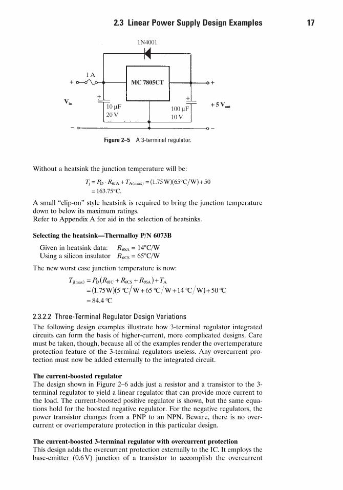
Without a heatsink the junction temperature will be:
A small “clip-on” style heatsink is required to bring the junction temperaturedown to below its maximum ratings.Refer to Appendix A for aid in the selection of heatsinks.
Selecting the heatsink—Thermalloy P/N 6073B
Given in heatsink data: RqSA = 14°C/WUsing a silicon insulator RqCS = 65°C/W
The new worst case junction temperature is now:
2.3.2.2 Three-Terminal Regulator Design VariationsThe following design examples illustrate how 3-terminal regulator integratedcircuits can form the basis of higher-current, more complicated designs. Caremust be taken, though, because all of the examples render the overtemperatureprotection feature of the 3-terminal regulators useless. Any overcurrent pro-tection must now be added externally to the integrated circuit.
The current-boosted regulatorThe design shown in Figure 2–6 adds just a resistor and a transistor to the 3-terminal regulator to yield a linear regulator that can provide more current tothe load. The current-boosted positive regulator is shown, but the same equa-tions hold for the boosted negative regulator. For the negative regulators, thepower transistor changes from a PNP to an NPN. Beware, there is no over-current or overtemperature protection in this particular design.
The current-boosted 3-terminal regulator with overcurrent protectionThis design adds the overcurrent protection externally to the IC. It employs thebase-emitter (0.6V) junction of a transistor to accomplish the overcurrent
T P R R R Tj D JC CS S A
W C W C W C W CC
max
..
( ) = + +( ) += ( ) ∞ + ∞ + ∞( ) + ∞= ∞
q q q A
1 75 5 65 14 5084 4
T P R Tj D JA A max W C W
= 163.75 C.
= ◊ + = ( ) ∞( ) +∞
( )q 1 75 65 50.
2.3 Linear Power Supply Design Examples 17
1N4001
+
-
Vin
+
10 mF20 V
MC 7805CT
100 mF10 V
+
+
-
+ 5 Vout
1 A
Figure 2–5 A 3-terminal regulator.

threshold and gain of the overcurrent stage. For the negative voltage version ofthis, all the external transistors change from NPN to PNP and vice versa. Thesecan be seen in Figures 2–7a and b.
2.3.3 Floating Linear RegulatorsA floating linear regulator is one way of achieving high-voltage linear regula-tion. Its philosophy is one in which the regulator controller section and theseries-pass transistor “float” on the input voltage. The output voltage regula-tion is accomplished by sensing the ground, which appears as a negative voltagewhen referenced to the output voltage. The output voltage serves as the “float-ing ground” for the controller and the power for the controller and series-passtransistor is drawn from the headroom voltage (the input-to-output difference)or is provided by an auxiliary isolated power supply.
18 An Introduction to the Linear Regulator
+Vin
Fuse
1N4001
Rsc
100W 2N6049
10uF 0.1uF
12N2955*
780X
3+Vout
* Heatsink required
Rsc =0.7V
Isc
2
(a)
(b)
1N4001
+Vin
Fuse Rsc
2N3055*
1 3+Vout
* Heatsink required
Rsc =0.7 V
Isc
10uF
2
790X1uF10uF
5.6W
10uF
Figure 2–7 (a) Positive current-boosted 3-terminal regulator with current limiting. (b) Negative current-boosted 3-terminal regulator with current limiting.
+Vin
Fuse1N4001
100W2N2955*
1 3
780X10uF
2
10uF
+Vout * Heatsink required
Figure 2–6 Current-boosted 3-terminal regulator without overcurrent protection.

The power transistor still needs to have a breakdown voltage rating greaterthan the input voltage, since at start-up, it must see the entire input voltageacross it. Other methods such as a bootstrap Zener diode can also be used inorder to shunt the voltage around the pass transistor, but only when the inputvoltage itself is switched on and off to activate the power supply. Also, cautionmust be taken to ensure that any controller input or output pin never goes negative with respect to the floating ground of the IC. Protection diodes areusually used for this purpose. One last caution is the little-known breakdownvoltage of common resistors. If the output voltage exceeds 200V, more than onesensing resistor must be placed in series in order to avoid the 250V breakdowncharacteristic of 1/4W resistors.
A common low-voltage positive floating regulator is the LM317 (the negativeregulator complementary part is the LM337). The MC1723 can also be used tocreate a floating linear regulator, but care must be taken to protect the ICagainst the high voltage.
2.3 Linear Power Supply Design Examples 19
39V, 1W
+Vin
+100 V
GND
+10uF150V
in outLM317
adj 4.7K
27K Iprog
+
100uF100V
GND
+75V
+Vout
5.6 V500mW
Figure 2–8 A high voltage floating linear regulator.
1N4937
BUX85 Rsc
62W+350V
210
Vo11TIP50
12K
12K3W
+400V
12
Vc
Vcc
REF6
5
1N414827K
(+)(–) Comp
VEE7
3CSLM723N
CL
+500uF400V
GND
13
47pF
4
33K
1N4148
1.5M
1.5M Isense = 116uAGND
1N5242+10uF450V
Figure 2–9 A 350 volt, 10 mA floating linear regulator.

The first example shows how an LM317 can be modified to create a 70Vlinear regulator from a 100 V input voltage. Several design restrictions must bestrictly followed, for example, the operational headroom voltage must notexceed the voltage rating of the bootstrap Zener diode or regulation will be lost.Also the use of the protection diode on the error amplifier is mandatory. Thisregulator can be seen in Figure 2–8.
The second example illustrates a 350V floating linear regulator that canprovide up to 10 mA of load current from a 400 to 450 V unregulated source.The TIP50 provides the bias supply for the controller, which must withstand thefull input voltage during start-up and power supply foldback. The controller is“grounded” on the output voltage and the minimum headroom voltage is 15 V.To readjust the output voltage, one changes the value of the two series resistorsin the voltage sensing branch and this is set by
(2.4)
Floating linear regulators are particularly suited for high-output voltage regu-lation, but may be used anywhere. This regulator can be seen in Figure 2–9.
R V Isense out senseV= +( )4 0.
20 An Introduction to the Linear Regulator

3. Pulsewidth Modulated SwitchingPower Supplies
21
Although pulsewidth modulated (PWM) switching power supplies have beenaround for a long time, it wasn’t until the mid-1970s that they became moreaccepted and broadly applied. Switching power supplies offer many advantagesover linear regulators.
Switching power supplies are more efficient and are smaller in size than linearregulators of similar ratings. They are, however, more difficult to design andradiate more electromagnetic interference (EMI).
Today, there are two ways to approach the design of switching power sup-plies. The design of board-level, dc/dc (dc-in, dc-out) switching power suppliescan be copied directly from the semiconductor maker’s datasheet and can usestandard components from other manufacturers. However, if any of the require-ments fall outside the standardized approaches, then it becomes a customdesign, and is much more complex.
This book is organized so that the massive process of designing a customswitching power supply is broken down into smaller, more understandablepieces. Each piece is then explained in “non-power engineer” terms, and com-monly accepted design approaches are illustrated with the relevant design equa-tions. The intent is for the reader to read the section, choose the best designapproach to meet his or her needs, use his or her particular system parameters,and produce a subcircuit that can be inserted into a larger power supply design.The design order is the way that seasoned power engineers use to approachtheir designs, and has proven to provide answers before the questions havearisen.
3.1 The Fundamentals of PWM Switching PowerSupplies
The operation of switching power supplies can be relatively easy to understand.Unlike linear regulators which operate the power transistor in the linear mode,the PWM switching power supply operates the power transistors in both the saturated and cutoff states. In these states, the volt-ampere product across thepower transistor is always kept low (saturated, low-V/high-I; and cutoff, Hi-V/No-I). This EI product within the power device is the loss within all the powersemiconductors.
This more efficient operation of the PWM switching power supply is done by“chopping” the direct current (dc) input voltage into pulses whose amplitude is
the magnitude of the input voltage and whose duty cycle is controlled by aswitching regulator controller. Once the input voltage is converted to an ac rec-tangular waveform, the amplitude can be stepped up or down by a transformer.Additional output voltages can be derived by adding secondaries to the trans-former. Ultimately these ac waveforms are then filtered to provide the dc outputvoltages.
The controller, whose main purpose is to maintain a regulated output voltage,operates very much like a linear style controller. That is, the functional blocks,voltage reference, and error amplifier are arranged identical to the linear regulator’s. The difference is, the output of the error amplifier (the errorvoltage) is then placed into a voltage-to-pulsewidth converter stage prior todriving the power switches.
There are two major operational types of switching power supplies: theforward-mode converter and the boost-mode converter. Although their arrange-ments of parts are subtly different, their operation is very different and eachhas advantages in certain areas of application.
3.1.1 The Forward-mode ConverterForward-mode regulators form a large family of switching power supply topolo-gies. They can be recognized by an L-C filter just after the power switch or afterthe output rectifier on the secondary of a transformer. A simple form of the forward-mode regulator can be seen in Figure 3–1. This is called the buckregulator.
Its operation can be seen as analogous to a mechanical flywheel and a one-piston engine. The L-C filter, like the flywheel, stores energy between the powerpulses of the driver. The input to the L-C filter (choke input filter) is the choppedinput voltage. The L-C filter volt-time averages this duty-cycle modulated inputvoltage waveform. The L-C filtering function can be approximated by
Vout ª Vin · duty cycle. (3.1)
The output voltage is maintained by the controller by varying the duty cycle.The buck converter is also known as a step-down converter, since its output mustbe less than the input voltage.
The operation of the buck regulator can be seen by breaking its operationinto two periods (refer to Figure 3–2). When the switch is turned on, the inputvoltage is presented to the input of the L-C filter. The inductor current rampslinearly upward and is described as
(3.2)iV V t
LiL on
in out on
o
init( ) =-( )
+ .
22 Pulsewidth Modulated Switching Power Supplies
+
–Vin
SW
D
IonIoff
Cout
+
Lo
+
Rload
–
Figure 3–1 A basic forward-mode converter (buck converter shown).

The energy stored within the inductor during this period is
(3.3)
This input energy is stored by the flux contained within the core material of theinductor.
When the power switch is turned off, the input voltage to the inductor wantsto fly below ground and the diode (D), called a catch diode, becomes forwardbiased. This continues to conduct the current that was formerly flowing throughthe power switch and some of the stored energy is discharged to the load. Thisforms a local current loop that includes the diode, inductor, and the load. Thecurrent through the inductor is described during this period by
(3.4)
The current waveform, this time, is a negative linear ramp whose slope is -Vout/L. When the power switch once again turns on, the diode snaps off andthe current now flows through the input power source and the power switch.The inductor’s current (imin) just prior to the switch being turned on, becomes the initial current the power switch must then initially pass.
The dc output load current value falls between the peak and the minimumcurrent values. In typical applications, the peak inductor current is about 150percent of the dc load current and the minimum current is about 50 percent.
The advantages of forward-mode converters are: they exhibit lower outputpeak-to-peak ripple voltages than do boost-mode converters, and they canprovide much higher levels of output power. Forward-mode converters canprovide up to kilowatts of power.
i iV t
LL off pk
out off
o
( ) = -◊
E L i istored o pk= ÊËÁ
ˆ¯ -( )1
2
2
min .
3.1 The Fundamentals of PWM Switching Power Supplies 23
Figure 3–2 The voltage and current waveforms for a forward-mode converter (buck converter).

A transformer can be placed between the power switch and the L-C filterwhich serves as a voltage step-up or step-down of the input voltage. Thesetopologies form a family of converters called transformer-isolated forward con-verters (refer to Figures 3–14 through 3–17). The transformer offers some dis-tinct advantages, such as providing a dielectric barrier from the input to theoutput and the ability to add additional outputs, and makes the output voltagesindependent from the level of the input voltage.
3.1.2 The Boost-mode ConverterThe second family of converters are the boost-mode converters. The most ele-mentary boost-mode (or boost-derived) converter can be seen in Figure 3–3. Itis called a boost converter.
As one can notice, the boost-mode converter has the same parts as theforward-mode converter, but they have been rearranged. This new arrangementcauses the converter to operate in a completely different fashion than theforward-mode converter. This time, when the power switch is turned on, acurrent loop is created that only includes the inductor, the power switch, andthe input voltage source. The diode is reverse-biased during this period. Theinductor’s current waveform (Figure 3–4) is also a positive linear ramp and isdescribed by
(3.5)i tV t
LL on
in on( ) =◊
24 Pulsewidth Modulated Switching Power Supplies
L
+
–Vin
IonIoff
SW
D +
Cout
Iload
Rload
–
+
Figure 3–4 Waveforms for a discontinuous-mode boost converter.
Figure 3–3 A basic boost-mode converter (boost converter shown).
Energy is stored in the flux within the inductor’s core material. When thepower switch is turned off, the inductor’s voltage, “flies back” above the inputvoltage. Quickly, the diode becomes forward biased when the inductor’s voltageexceeds the output voltage. The inductor voltage is then clamped at the valueof the output voltage. This voltage level is referred to as the flyback voltage andis the value of the output voltage plus one diode forward voltage drop. Theinductor current during the power switch’s off period is described by
(3.6)
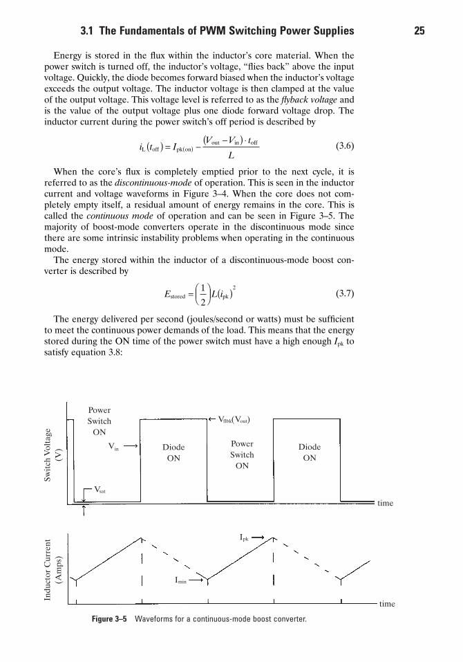
When the core’s flux is completely emptied prior to the next cycle, it isreferred to as the discontinuous-mode of operation. This is seen in the inductorcurrent and voltage waveforms in Figure 3–4. When the core does not com-pletely empty itself, a residual amount of energy remains in the core. This iscalled the continuous mode of operation and can be seen in Figure 3–5. Themajority of boost-mode converters operate in the discontinuous mode sincethere are some intrinsic instability problems when operating in the continuousmode.
The energy stored within the inductor of a discontinuous-mode boost con-verter is described by
(3.7)
The energy delivered per second (joules/second or watts) must be sufficientto meet the continuous power demands of the load. This means that the energystored during the ON time of the power switch must have a high enough Ipk tosatisfy equation 3.8:
E L istored pk= ÊËÁ
ˆ¯ ( )1
2
2
i t IV V t
LL off pk on
out in off( ) = --( ) ◊
( )
3.1 The Fundamentals of PWM Switching Power Supplies 25Sw
itch
Vol
tage
(V)
Indu
ctor
Cur
rent
(Am
ps)
PowerSwitch
ON
Vin
Vsat
DiodeON
Vflbk(Vout)
PowerSwitch
ON
DiodeON
time
time
Ipk
Imin
Figure 3–5 Waveforms for a continuous-mode boost converter.

(3.8)
where fop is the frequency of operation of the converter.The boost converter shown in Figure 3–3 can only be used as a step-up con-
verter. That is, the output voltage must be higher than the highest value of inputvoltage input. If the inductor is replaced by a transformer, as seen in Figure3–15, a topology called a flyback converter is made. The flyback voltage andcurrent, as seen by the power switch, are similar to those in the boost converter,but are affected by the turns ratio of the transformer. The flyback voltage, whichis still Vout + Vdiode on the secondary, is scaled by the turns ratio of the trans-former when viewed from the power switch. The transformer also provides adielectric barrier from the input to the output, and additional output voltagescan be derived from the same transformer. The outputs also become indepen-dent from the level of the input voltage, thus giving the flyback topology thehighest input dynamic range of all the topologies.
Due to the higher peak currents within boost-mode converters, they can onlybe used in applications of 150W or less. They have the least parts of all the topologies and are therefore very popular in the low to medium power applications.
3.2 The Building-block Approach to PWM SwitchingPower Supply Design
PWM switching power supplies lend themselves quite nicely to an organizedapproach to their design. They are more complicated and therefore can be par-titioned into more functional blocks of an elementary nature. The switchingpower supply designer, whether knowingly or unknowingly, does its design in afunctional block approach and this approach will be presented.
Executing the design in a specific order and fashion makes the design flowmuch easier by predetermining information needed for subsequent portions. Ingeneral, PWM and resonant switching power supply designs start with theoverall considerations, next comes the design of the power sections, then thedesigns proceed through the control and ancillary functions, and finally is the testing and perfecting stage. It all begins with a well-defined design specifi-cation as outlined in Section 1.3. By first defining the operation of the supplyand the environment in which it must operate, the design flow takes the formas seen in Figure 3–6. Some initial decisions must be made at the beginning,namely which topology of switching power supply to use.
Once the topology is selected, the design path is determined and the designmay proceed. By proceeding through the block diagram in Figure 3–7, in theorder indicated by the design flow in Figure 3–6, the design will progress rela-tively quickly. The first-time designer may be able to produce a very good “paperdesign” (or schematic) within 8 working hours, if he or she has a good libraryof data books. Each functional block in Figure 3–7 will have a choice of typicaldesign approaches for that block. The designer determines from his or herrequirements which approach is most appropriate for the needs of the supply.Then, by executing the design equations and using the parameters supplied bythe design specification, the block can be designed within a matter of minutes.
P P f L Iload out op pk< = ( )( )È
Î͢˚
1
2
2
26 Pulsewidth Modulated Switching Power Supplies

3.2 Building-block Approach to Switching Power Supply Design 27
Figure 3–6 Design flow for a PWM switching power supply.

3.3 Which Topology of PWM Switching Power Supply to Use?
A major decision that must be considered at the beginning of a switching powersupply design is which basic topology to use. The term topology refers to thearrangement of the power components within the switching power supplydesign. This arrangement has a large bearing on which environment the supplycan operate in safely and how much power the power supply can provide to theloads. This is the point in the design process where the major cost versus per-formance tradeoffs are made. Each topology has its relative merit. One topol-ogy may have a low parts cost, but can only provide a limited amount of power;another has ample power capability, but costs more, and so on. More than onetopology will work for any application, but one of the choices may provide thebest performance at the needed cost. A summary of the relative merits of thevarious topologies is given in Table 3–1.
The major factors that determine the optimum choice of topology are:
1. Is transformer isolation needed from input to output?2. How much input voltage appears across the primary winding of the trans-
former or inductor?3. What is the peak current through the power switches?4. What is the maximum operating voltage across the power switches?
The nontransformer isolated topologies are used for board-level converters.These are in distributed power systems where an intermediate bus voltage isdistributed throughout the system and each board within the system has its ownpower supplies. The bus voltage is always a “safe” level that is not deemed lethalto the operator of the equipment, therefore dielectric isolation is optional. I stillheartily recommend transformer isolation in most applications. The added cost
28 Pulsewidth Modulated Switching Power Supplies
Figure 3–7 The functional block diagram for a PWM switching power supply.

is minimal compared to the added level of protection for the load. Transformerisolation is mandatory for all switching power supplies having a dc input voltageof 40VDC or higher.
The amount of voltage appearing across the primary of the transformer isindicative of how much peak current is flowing through the power switches.Switching power supplies are constant power circuits. That is, the lower theprimary voltage, the higher the peak currents in order to provide the neededoutput power. For power transistors and MOSFETs in TO-220 packages andsmaller, a maximum peak current limit of 20A is recommended. Above 20A,the failure modes of the power switches become very erratic and the powerdevices are difficult to protect. By using another topology, the peak current canbe reduced.
The higher the maximum voltage the power switches experience, the greaterthe likelihood that they will exceed their safe operating areas (SOA). Voltagespikes are very common within switching power supplies, and the opportunityof these spikes exceeding the avalanche voltage rating of the power switchbecomes more likely. For transformer isolated topologies, the industry hassettled into certain topologies that they use within the different ranges of appli-cations. This is shown in Figure 3–8.
The flyback topology (see Figure 3–12) is the favorite below 100 to 150Wbecause of its low parts count (hence cost) and intrinsically better efficiency.But because its peak currents are much higher than the forward-mode con-verters, it reaches the SOA limits of the power switches at a relatively low outputpower. Between an output power of 150 and 500 W the half-bridge (see Figure3–15) becomes the favorite. The parts cost more but they are still reasonable.The half-bridge converter only places one-half of the input voltage across theprimary winding and therefore exhibits fairly high peak currents. It therefore isonly used to 500W or less. Above 500W and into many kilowatts, the full-bridge(see Figure 3–16) topology is used. This requires four power switches, two ofwhich have floating drive circuits, and is the most costly to implement, but atthese output power levels the added cost is necessary. The push-pull (see Figure3–14) can also be used in this region, but it suffers from a potentially severefailure mode called core imbalance. This is where the flux within the transformerwill operate non-symmetrically about a “zero” balance point. This will cause the
3.3 Which Topology of PWM Switching Power Supply to Use? 29
Table 3–1 Comparison of the PWM Switching Regulator Topologies

transformer to saturate in the direction of one power switch and burn it outwithin nanoseconds when step changes occur in the load. Pulse-to-pulse current-protected voltage-mode control or current-mode control techniques must beused to avoid this problem.
By reviewing Table 3–1 and Figure 3–8, you can develop a good idea as towhere your application fits. The appropriate topology then can be chosen.Figures 3–9 through 3–16 show the basic PWM switching power supply topologies along with their salient waveforms and some estimated importantparameters.
30 Pulsewidth Modulated Switching Power Supplies
1000
100
62V
10
10 100 1000
Output Power (Watts)
Buck
Non-Isolated
Full-Bridge
Very HighPeak Currents
Full-BridgeFlyback
Half-Bridge
DC
Inp
ut V
olta
ge (
Vol
ts)
+
Vin
–
Cin
Controlfeedback
D
PowerSwitch
L
+
+ Vout
Cout
–
Ipk ª1.4(Pout)
Vin(min)
Vsw ª Vin
Pout ª 0 W – 1 kW
VD
0Vfwd
IL
Ipk
Iload
0
Imin
time
time
Vin
Figure 3–8 Where various topologies are used.
Figure 3–9 The buck (step-down) converter.

3.3 Which Topology of PWM Switching Power Supply to Use? 31
Figure 3–10 The boost (step-up) converter.
Figure 3–11 The buck-boost converter.
Ipk ª5.5(Pout)
Vin(min)
Vsw ª Vout = Vflyback
Pout ª 0 W – 100 W
+
Vin
–
Cin Control
L
DSW
Cout
+
+
Vout
–
VSWVin
0
Vout
Vsat
ISWoff
SWon
Don
time
timeIDISW
Ipk
0
IL
+
–
Vin
Cin
Control SWD
Cout
Vout
–
+feedback
Vin
0
–Vout
Ipk
IL
0Isw ID
time
time
Ipk ª5.5(Pout)Vin(min)
Vsw ª Vin + abs(Vout)
Pout ª 0 W – 100 W
L+

32 Pulsewidth Modulated Switching Power Supplies
Figure 3–12 The flyback converter.
+
–
Vin CinControl
n1
D
Cout Vout
+
feedback
Vin
0
0
Ipri
Ipk
time
SW
–
time
Imin
Vsat
–2Vin
n2 +Ipk ª
2.8(Pout)Vin(min)
VSW ª 2Vin
Pout ª 0 – 300 W
T
VSW
LO
Figure 3–13 The one-transistor forward converter.
+
–
Vin Cin Control
n1
D
CoutVout
+
feedback
0
Vin
Ipri
0
Isec
Isw
time
time
SW
–
time
ID
Ipk
Vsat
Vinflybk
n2 +
Ipk ª5.5(Pout)Vin(min)
VSW ª Vin + Vout
Pout ª 0 W – 150 W
n1n2
0Vsw

3.3 Which Topology of PWM Switching Power Supply to Use? 33
+
–
VinCin
Control
SW1 D1
Cout Vout
+
feedback
Vin
0
0
ISW1 Ipk
time
SW2–
time
Imin
Vsat
–2Vin
D2+
Ipk ª1.4(Pout)Vin(min)
VSW ª 2Vin
Pout ª 0 –1 KW
T
VSW1
LO
SW1
SW2
Figure 3–14 The push-pull converter.
+
-
Vin Cin
Control
XFMRSW1
SW2
n2
n1
DsLo
Cout
+
-
Vout
C
C
T
feedback
Ipk ª2.8 (Pout)
Vin(min)
VSW ª Vin
Pout ª 0 - 500 W
Vin
2VSW2
-
0
ISW2
0Imin -
Ipk
- Vin
Vsat SW2
SW1
time
time
+
Figure 3–15 The half-bridge converter.

34 Pulsewidth Modulated Switching Power Supplies
+
-
Vout
Ipk ª1.4 (Pout)
Vin(min)
VSW ª Vin
Pout ª 0 - 1 kW+
Lo
Ds
Cout
+
XFMRSW3
CTn2
n1
SW1
SW2
XFMR
ControlCin
+
Vin
-SW4
Vin
2VSW2
0
ISW2
0
Imin -
Ipk
- Vin
Vsat SW2–3
SW1–4
time
time
Figure 3–16 The full-bridge converter.
3.4 The “Black Box” Considerations for SwitchingPower Supplies
This preliminary step in the design phase, predetermines some of the majorparameters the switching power supply will exhibit. This allows the designer to determine whether his or her choice of topology is correct and also allowsthe designer to order components for the breadboard, long before they arerequired. It also results in knowing some of the particularly important parame-ters needed later during the design. For determining the “black box” estimates,the designer need only know the environmental parameters from the designspecification and then treat the future power supply as a black box; that is, abox with only input and output lines emerging from it (refer to Figure 3–17).
The estimates are done as follows:
1. Output power
(3.9)
2. Input power
(3.10)PP
inout
effic est@
( )
P V Im m
m
n
out out out= ◊( )( ) ( )=
Â1
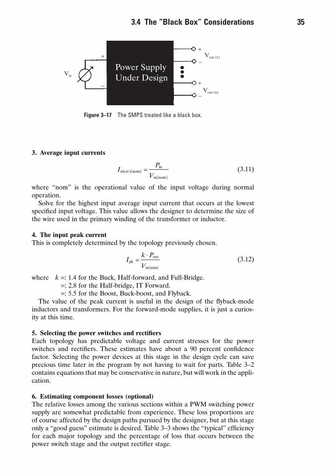
3. Average input currents
(3.11)
where “nom” is the operational value of the input voltage during normal operation.
Solve for the highest input average input current that occurs at the lowestspecified input voltage. This value allows the designer to determine the size ofthe wire used in the primary winding of the transformer or inductor.
4. The input peak currentThis is completely determined by the topology previously chosen.
(3.12)
where k =: 1.4 for the Buck, Half-forward, and Full-Bridge.=: 2.8 for the Half-bridge, IT Forward.=: 5.5 for the Boost, Buck-boost, and Flyback.
The value of the peak current is useful in the design of the flyback-modeinductors and transformers. For the forward-mode supplies, it is just a curios-ity at this time.
5. Selecting the power switches and rectifiersEach topology has predictable voltage and current stresses for the powerswitches and rectifiers. These estimates have about a 90 percent confidencefactor. Selecting the power devices at this stage in the design cycle can save precious time later in the program by not having to wait for parts. Table 3–2contains equations that may be conservative in nature, but will work in the appli-cation.
6. Estimating component losses (optional)The relative losses among the various sections within a PWM switching powersupply are somewhat predictable from experience. These loss proportions areof course affected by the design paths pursued by the designer, but at this stageonly a “good guess” estimate is desired. Table 3–3 shows the “typical” efficiencyfor each major topology and the percentage of loss that occurs between thepower switch stage and the output rectifier stage.
Ik P
Vpk
out
in min
=◊
( )
IP
Vin av nom
in
in nom
( )( )( )
=
3.4 The “Black Box” Considerations 35
Vin
+
-
+
-
+
-
Vout (1)
Vout (n)
Power SupplyUnder Design
Figure 3–17 The SMPS treated like a black box.

To determine each section’s respective loss for your power supply topology,use the following
(3.13)
where P(%) is the typical estimated percentage loss of the desired section withrespect to the total loss of the power supply (see Table 3–3).
When the topology has multiple power switches, then multiply the Ploss(ckt)
by
0.5 (50%) for the push-pull and half-bridge0.25 (25%) for the full-bridge.
To estimate the loss within each output rectifier within a multiple outputswitching power supply, use the ratio of the desired output’s power comparedto the total output power as in Equation 3.14.
(3.14)
These loss figures can be used in determining the appropriate packagesneeded for the semiconductors. That is, do some of the semiconductors need
P P P
P
Pn
nr in
out
out
effic( ) ( )( )ª ◊ -( ) ◊ ◊
ÊËÁ
ˆ¯
1 %
P P Ploss ckt in 1 effic( ) ( )= ◊ -( ) ◊ %
36 Pulsewidth Modulated Switching Power Supplies
Table 3–2 Estimating the Significant Minimum Parameters of the PowerSemiconductors

to be attached to a heatsink? Also, a guess at how much heatsinking is requiredcan be made.
This completes the black box estimates portion of the design program. As onecan see, some very useful information can be determined by performing theseestimates.
3.5 Design of the Magnetic Elements
The design of the magnetic elements forms the backbone of a good switchingpower supply design. Their proper electrical and physical design have a largeaffect on the reliable operation of every switching power supply design. Entirebooks have been written devoted to their design and theory, but in keeping withthe premise behind this publication, I have chosen to take a different approach.Since switching power supplies are a specialized narrow application of magneticelements, the design process for the magnetic elements can be greatly focusedand simplified. This yields the quickest working design without having to under-stand the subtleties involved with each facet of the design. For more detail inthe operation of the core materials, refer to Appendix D.
3.5.1 The Generalized Design Flow of the Magnetic ElementsPart of the confusion in designing the magnetic elements is the inexactnessinvolved in their design. At best, the results of calculations should be considereda “calculated estimate.” Pushing the result of a calculation in one direction oranother will still yield a working design, but may offer advantages in some otherfacet of the power supply design such as core size, power supply input dynamic
3.5 Design of the Magnetic Elements 37
Table 3–3 The “Black Box” Estimates for Losses within the Various Topologies

range, etc. These trade-offs will be discussed at the appropriate points in thetext.
The generalized design flow for the magnetic elements is as follows.
1. Select the core material appropriate for the application and for the fre-quency of operation (Appendix D).
2. Select the desirable core style that will meet the needs of the applicationand of any regulator agency the power supply should meet (Appendix D).
3. Determine the size of the core needed to provide the required outputpower of the power supply (Section 3.5.2).
4. Determine whether an airgap is needed and calculate the number of turnsneeded for each winding. Then determine whether the accuracy of theoutput voltages meets the needs of the requirements and whether thewinding actually fit into the selected core size (Sections 3.5.3 through3.5.7).
5. Wind the magnetic component using the described physical winding tech-niques given in Section 3.5.9.
6. During the prototype stage, verify its operation with respect to the levelof voltage spikes, cross regulation, output accuracy and ripple, and RFI,etc., and make corrections where necessary.
If the above procedure is executed, the initial design of any magnetic com-ponent should take less than 30 minutes. Please refer to the end of AppendixD for the listing of the core manufacturer’s websites where the needed information can be downloaded.
3.5.2 Determining the Size of the Magnetic CoreEach manufacturer uses different core sizing procedures. Some use graphs,others simply state how much power each core can handle for a particular application, and some use cryptic equations that are confused by the mixture ofunrelated units. The following two procedures are generalized approaches forestimating the initial core size.
The following methods take two forms. The first is a simple table of size versuspower which yields a good “guess” if you do not have many or complicated wind-ings. The second is a calculated approach which has “fudge factors” that involvethe number of windings, and whether the component must meet a regulatoryagency requirement. The results of both should be considered estimates, sosamples of the resulting core size should be requested along with samples of thenext larger size. This will eliminate the need to go back later if the windingsgrow too large for the core.
There are five major factors in selection of the size of a core for an application:
Factor: Parameter Affected:Output power Ac (core cross sectional area)Bipolar or unipolar flux Ac (core cross sectional area)Input voltage Aw (window area)Number of windings Aw (window area)Winding configuration Aw (window area)
Other considerations enter into the operation of the magnetic element, suchas the desired range of leakage inductance for each winding, electrostatic shield-ing, etc. (see Appendix D). These factors affect the size and cost of the finalmagnetic element.
38 Pulsewidth Modulated Switching Power Supplies

Core Sizing Method 1Use Table 3–4 to determine the range of power into which your application fits.Consult a core manufacturer’s data book for cores that fit your application andselect the closest or next larger size of core. Order those samples (refer to Table3–4).
Core Sizing Method 2This method begins with the assumption of a one-winding transformer. Eachwinding and each additional regulatory requirement only tend to make thewinding area and hence the core to grow. The influences of each of the factorsare multiplied together to arrive at a combined “scaling factor.” The scalingfactor is then used to scale the size of the basic one-winding inductor.
The first step is to determine the size of the one-winding inductor. This isfound by using Equation 3.15.
(3.15)
where: dw is the area of the wire used in the primary winding in circularmils or square inches (refer to the wire table in Appendix E).
Bmax is the peak operating flux density (G).f is the frequency of operation.
Pout is the total output power of the supply.For the MKS (pure metric) system the following equation is used:
(3.16)
where: dw is the area of the wire used in the primary winding in cm2 (referto the wire table in Appendix E).
Bmax is the peak operating flux density (Teslas).f is the frequency of operation (Hz).
Pout is the total output power of the supply (W).Next the scaling influences need to be identified and a combined scaling factor
calculated. These scaling factors are found in Table 3–5.Combine the individual scaling factors as follows:
Knet = Ka ·Kb . . . etc. (3.17)
The estimated size for the final transformer is obtained from:
Wa Ac¢ = Knet ·Wa Ac (3.18)
W AP d
B fa c
out w=◊ ◊
◊
0 68.
max
W AP d
B fa c
out w=◊ ◊ ◊
◊
0 68 103.
max
3.5 Design of the Magnetic Elements 39
Table 3–4 Approximate Core Size versus Output Power

In the U.S., the result will be in inches4; for the metric system the results willbe in meters4. The relationship to convert between the two numbering systemresults is
meters4 = 2.402 ¥ 106 inches4 (3.19a)
inches4 = 4.162 ¥ 10-7 meters4 (3.19b)
Some of the core manufacturer’s data sheets specify a core parameter WaAc
that can be compared with the results of the above calculations. The core withthe closest or next higher value should be chosen.
If you desire to use the core manufacturer’s own method of determining coresize, then feel free to do so. This phase of the transformer design is a gross estimation.
3.5.3 Designing the Forward-mode TransformerThere are two main functions the forward-mode transformer performs: the firstis to provide a dielectric isolation barrier from the input to the output; and thesecond is to step up or step down the pulsewidth modulated ac input voltagesignal. The design flow becomes a step-by-step design procedure.
The forward-mode transformer stores no energy other than a small amountwithin the magnetization of the core material itself. There are only two majorconsiderations which are important during the gross schematic design of thetransformer:
1. The peak operating flux density (Bmax) should never closely approach orenter saturation over the power supply’s entire operating range.
2. Do the resulting windings provide an accurate enough output voltage tomeet the design specifications?
Other considerations are important during the physical winding process andinvolve winding losses, leakage inductance, shielding, and physical space. Theydo not need to be considered now.
The first step is to determine the number of turns needed for the primarywinding. For this, the parameters from the core data sheet of the particular coreand core material are used. Also, the minimum level of flux density alreadyshould have been determined (refer to Appendix D). The equation for determining the number of turns for the primary winding in the CGS System(U.S.) is
(3.20a)NV
f B Apri
in nom
max c
=◊
◊ ◊ ◊( ) 10
4
8
40 Pulsewidth Modulated Switching Power Supplies
Table 3–5 Transformer Growth Scaling FactorsConsideration Scaling Factor
Flyback transformer 1.1One secondary 1.2 orTwo or more secondaries 1.3 orIsolated secondaries 1.4UL or CSA approval 1.1 orIEC approval 1.2Faraday shield 1.1
}}
}

where Ac is the effective core cross sectional area of the desired core(cm2).
Vin(nom) is the typical operating input voltage (V).Bmax is the maximum operating flux density (gauss (webers/cm2)).
In the MKS System (Europe) system this is
(3.20b)
where Ac is the effective core cross sectional area of the desired core(m2).
Vin(nom) is the typical operating input voltage (V).Bmax is the maximum operating flux density (teslas (webers/m2)).
Some core companies use still a third metric system, milliTeslas (mT), andmillimeters. These companies tend to be Japanese.
(3.20c)
where Ac is the effective core cross sectional area of the desired core(mm2).
Vin(nom) is the typical operating input voltage (V).Bmax is the maximum operating flux density (mT (webers/mm2)).
This number of turns now serves as the reference winding upon which all theother windings will be determined.
Next, one determines the number of turns of the highest power output sec-ondary winding. The voltage drop across the output rectifiers cannot be ignored.The equation to determine the number of turns for this winding is
(3.21)
where Vfwd is the forward voltage drop of the anticipated output rectifier.DCmax is the maximum expected duty cycle (0.95 is good).Vin(min) is the minimum expected input voltage.
This equation can be solved for the needed secondary turns at the lowestanticipated input voltage. At any input voltage lower than that, the regulatorwill fall out of regulation.
The next step is to determine the number of turns for the other secondariesbased on the turns of the first secondary winding. The starting point is
(3.22)
where Vout(n) is the additional output voltage.VD is the anticipated rectifier’s forward voltage drop.
The result of this calculation will always yield a noninteger number, but manycores can only accept an integer number of turns. Therefore, one must roundoff the results to the closest integer. This results in an error in the eventualoutput voltages of these additional outputs. One must now check to see if theseerrors are too much for the application. Using the original output’s “volts perturn” value, calculate the new output voltages using the rounded-off turns onthe additional windings. If the error in any of the output voltages is too great,first consider changing the technology of the rectifier—to one that has a higher
NV V N
V Vn
nsec
out D sec 1
out 1 D1
( )( ) ( )
( )=
+( )+( )
NV V
N Vsec
out fwd
pri in min maxDC=
+( )( )( )
1 1.
NV
f B Apri
in nom
c
=◊
◊ ◊ ◊( ) 10
4
9
max
NV
f B Apri
in nom
max c
=◊ ◊ ◊
( )
4
3.5 Design of the Magnetic Elements 41

or lower forward voltage drop. If that is insufficient, add a turn to the originaloutput winding, recalculate the new value for the additional turns, and recheckthat the error is acceptable. If the result is still unacceptable, go back to theprimary and add turns and recalculate the new secondaries. Remember thatadding turns on the primary winding is moving in the safe direction of lowerflux density and adding turns to the secondary makes the power supply fall outof regulation at a lower input voltage. This iterative process should continueuntil all the outputs have an acceptable amount of error from the “ideal” outputvoltage. The designer will have to accept some error in the output voltages asa fact of life.
The next step is to decide how the secondary windings should be arranged.That is, whether it is desired to have isolated secondaries, center-tapped or non-center-tapped, or have “autotransformer” style secondaries that share windingsof lower voltage outputs (refer to Figure 3–18).
Remember that the amount of current flowing through each half of a center-tapped winding is one-half the continuous current and therefore needs only one-half the wire cross-sectional area. Also, autotransfomer windings have morethan one output current flowing though the lower winding, so adjustments tothe wire gauges are necessary.
Lastly in the “paper design,” the designer should verify that the turns andtheir respective wire gauges fit inside the area reserved for windings. This isdone by summing the products of each winding times its respective wire cross-sectional area and verifying that the sum is less than the winding area specifiedfor the core or bobbin.
(3.23)
where k is the between 1.2 and 1.4 for winding inefficiencies and insulating tape.The final design step is the method for physically building the transformer;
for this refer to Section 3.5.8.
3.5.4 Designing the Flyback TransformerThe flyback transformer operates differently from the forward-mode trans-former. Instead of both windings conducting current simultaneously, energy isstored within the core material by the primary winding and then transferred tothe secondary circuit when the primary turns off. Accordingly, the classic trans-former relationships of reflected impedances and primary-to-secondary turnsratios do not apply directly. Now the voltage, time, and energy become the mainconcerns.
To start the design, the peak current should have been estimated during theproceeding “black box” estimation phase. The core style and material shouldhave also been selected (refer to Appendix D). This time an air gap is neces-sary for reliable operation.
One begins by realizing that the primary winding behaves like an elementaryinductor during the power switch’s on-time and obeys the relationship in Equation 3.24:
(3.24)
Rearranging for Lpri and substituting Ton = ∂(max)/f, one can solve for themaximum primary inductance using known power supply operating parametersusing Equation 3.25:
IV T
Lpk
in on
pri
=◊
W k N Ai ia wª ◊ ◊( )( )Â
42 Pulsewidth Modulated Switching Power Supplies

(3.25)
where ∂(max) is the maximum duty cycle (usually 50 percent or 0.5).This inductance value should be considered the maximum value since any
higher value will cause the power supply to fall out of regulation above theminimum operational input voltage.
The energy entering the core during each on time of the power switch is
(3.26)EL I
storedpri pk=
◊ ( )2
2
LV
I fpri
in min
pk
=◊
◊( ) ∂max
3.5 Design of the Magnetic Elements 43
L1
L2
+ Vout+
+GND
-Vout
Transformer
Simple. Stacked.
L2
Li+Vout2
+Vout1
Return
Transformer
(a)
TransformerTransformer
L+Vout
Return(GND)
Simple.
L1
L2
+Vout1
+Vout2
Return (GND)
Stacked.
(b)
L1
L2
+Vout2
Return2
+Vout1
Return1Transformer
Full Wave.
L2
L1
+Vout2
Return2+Vout1
Return1Transformer
Center-Tapped.
(c)
+
+
Figure 3–18 Forward-mode secondary winding arrangements: (a) center-tappedsecondaries; (b) full-wave secondaries; (c) isolated secondaries.

To verify that the maximum continuous output power capability of the trans-former can satisfy the maximum power requirements of the load, one calculates
(3.27)
An air-gap is required for all unipolar flux drive applications such as this. Onemethod of achieving this is shown in Equation 3.28a (CGS system (U.S.)).
(3.28a)
where Ac is the effective core cross-sectional area (cm2).Bmax is the maximum operational flux density (gauss (webers/cm2)).
In the MKS (Europe) system:
(3.28b)
where Ac is the effective core cross-sectional area (meters2).Bmax is the maximum operational flux density (T (webers/m2)).
This is an estimated air-gap length. The designer should use the closest valueof air-gap available within the standard core part number.
The core manufacturer provides a parameter called AL for each airgap length.This parameter is the inductance of the core when 1,000 turns is placed on it(U.S.). To determine the number of turns required to achieve the desired valueof inductance one solves Equation 3.29:
(3.29)
where Lpri is the value of the primary inductance in mH.If the AL value is not given for a particular core/air-gap combination, Equa-
tion 3.30 can be used. Do not mix CGS and MKS units (gauss and centimeterswith teslas and meters).
(3.30)
This value of Npri represents the maximum value of primary inductance that canplace the required energy in the core within the time period available at thelowest expected input voltage. Any future modifications to this number shouldbe in the downward direction.
Now determine the turns of the highest power secondary winding by usingEquation 3.31.
(3.31)
where ∂max is the maximum on-time duty cycle (usually 50 percent).The result of Equation 3.31 should be viewed as the maximum number of
turns, since any more turns would increase the secondary’s inductance and takelonger to empty the core’s energy. This calculation will always result in a non-integer number of turns. Many cores do not support fractional turns, so roundthis number to the closest fractional turn that the core will allow.
NN V V
Vsec
pri out fwd
in min
=+( ) - ∂( )
◊( )
( ) ( )
1 max
max∂
NB l
Ipri
gap actual
pk
= ( )max
.0 4p
NL
Apri
pri
L
= 1 000,
lL I
A Bgap
pri pk
c
metersª0 4 2
2
.
max
p
lL I
A Bc
gappri pk cmª
◊0 4 102 8
2
.
max
p
P L I f Pin core pri pk op out( ) = ( ) ◊ >1
2
2
44 Pulsewidth Modulated Switching Power Supplies

To determine the turns for any additional windings, use the procedure givenfor the forward-mode transformer (refer to Equation 3.22). Once again, if theresulting errors in the output voltages from the “ideal” values of output voltageare excessive, an iterative process will have to be under taken. Start by remov-ing one turn from the original secondary winding and recalculating the outputvoltages (including the forward voltage drops of the rectifiers). Eventually, someerror will have to be accepted in the output voltages.
The arrangement of the secondary should now be considered. The designermay either want to choose autotransformer style secondaries (i.e., shared turnswith lower voltage windings) or isolated windings. Since flyback secondaries arehalf-wave rectified, noncenter-tapped winding or full-wave rectifier bridges are not possible (refer to Figure 3–19). When the desired secondary windingarrangement is decided, the windings must be checked to see if they still fitwithin the core’s winding area. This is done in the same fashion as seen in Equa-tion 3.23.
The physical design of the transformer is critical in flyback converters. If they are not properly designed physically, excessive voltage spikes could begenerated that would adversely affect the reliable operation of the semi-conductor components (refer to Section 3.5.8).
3.5 Design of the Magnetic Elements 45
Figure 3–19 Flyback transformer secondary arrangements: (a) center-tapped secondaries;(b) isolated secondaries.

3.5.5 Designing the Forward-mode Filter ChokeThe forward-mode filter choke is the inductor filter on every forward-mode con-verter’s output. Its purpose is to store energy for the load during the periodswhen the power switch(es) are turned off. Its electrical function is to integratethe rectangular switching pulses into dc.
Its design is somewhat simple. First, the core should be chosen. Usually, amopermalloy toroid is used for this application. This is because this material isself-gapped. Gapped ferrite cores can also be used with no difficulties. If agapped ferrite core is desired follow the core sizing procedure in Section 3.5.2for a simple one-winding inductor. The following method will demonstrate howto design a choke using the mopermalloy toroid.
The first step is to determine the minimum inductance needed for the output,using Equation 3.32:
(3.32)
where Vin(max) is the highest peak voltage following the output rectifier of thatparticular output.
Vout is the output voltage.Toff(est) is the estimated on time of power switches at the highest input
voltage (30 percent of 1/fop is a good guess).Iout(min) is the lightest expected load current for that output.
This value represents the minimum value for the inductance, below which thecore will empty of flux at the minimum rated load current for that output.
For mopermalloy toroids, the method for estimating the needed core size isdone by calculating an intermediate value of the energy being stored in the core,using Equation 3.33:
(3.33)
Refer to Figure 3–20 and locate this value on the x-axis and move vertically untilthe first curve is intersected. Then move horizontally and read the part number.Then referring to that part number’s data sheet and reading the value of ALfor the core, the designer can calculate the number of turns needed by usingEquation 3.29. In general, the higher the average current flowing through thechoke, the lower the recommended permeability of the MPP core material.
Next the designer must check whether the turns will fit into the window orwinding area of the toroid. The percent of occupied window area is determinedby
(3.34)
where Awire is the cross-sectional area of the wire (refer to the wire tablein Appendix F) (in2 or m2).
Awindow is the available wire area of the toroid (window area) (in2 orm2).
N is the number of turns.If this value is greater than 40 to 50 percent, then too much of the window istaken up by the wire. This is because a winding shuttle must fit through thatremaining hole and it cannot pass through in less than 50 percent of the avail-able window area. The solution is to go to the next larger core size or to dropthe wire gauge by one size. The latter will increase the temperature of the induc-tor through added resistive losses.
% window wire
window
=◊ ( )N A
A100
E L IL out av2= ◊ ( )
LV V T
Imin
.=
-[ ] ◊
◊( ) ( )
( )
in max out off est
out min1 4
46 Pulsewidth Modulated Switching Power Supplies

Lastly, if the supply operates at a high frequency and the current through thefilter is high, then the one might consider using litz wire, which is a wire madeup of much smaller gauge wires to reduce the skin effect. Litz wire has an overalllarger diameter than single-strand wire with the same overall cross-sectionalarea.
3.5.6 Designing the Mutually Coupled Forward-mode Filter ChokeWithin multiple-output forward converters, it is possible to easily combine thefilter chokes of complementary outputs (i.e., +/- 5V, etc.) together on the samecore (see Figure 3–21). This offers several advantages; it saves space, vastlyimproves cross-regulation of those outputs, and exhibits superior ripple voltagelevels on both outputs.
First the core style and material should be selected. This is done in an iden-tical fashion as the single-output filter choke. Either a mopermalloy (MPP)toroid (refer to Section 3.5.5) or a ferrite bobbin core (refer to Section 3.5.2)
3.5 Design of the Magnetic Elements 47
Figure 3–20 DC bias core selector chart (L = inductance with dc bias in millihenries; I = dccurrent in amperes) (Courtesy of Magnetics, Inc.).

can be used. For the MPP toroid core, determine the size of the core needed,add the two load currents together, use the appropriate wire gauge for thiscurrent, and use Equation 3.33 for the toroid. The necessary core winding areawill be almost twice as large as for the single-winding choke.
The number of turns for both windings is determined by calculating theminimum inductance and the number of turns for the lowest current output.This is done using Equations 3.32 and 3.29. The other winding will have theidentical number of turns.
These windings should be bifilar wound, which means that the wires aretwisted together prior to winding them on the core or bobbin. This guaranteesthat the turns will be identical, which is critical for its operation. A twist pitchof about three twists per linear inch is good for #22 AWG and a lower twistpitch works for larger gauge wires.
The fluxes contributed by both windings should add within the core. Since thewinding sense (i.e., wound in the same direction) and the voltage polarities areboth opposite in complementary output, then the polarity dots should be onopposite sides of the inductor (see Figure 3–20). If the windings are mistakenlyhooked up in the wrong polarity, the windings will fight one another and theoverall operation of the power supply will be impaired.
More windings could be added to the mutually coupled filter choke core, butI highly recommend against this temptation. If the windings are not exact (tothe turn), the supply will loose approximately 1 percent in efficiency for eachturn in error on each output. Instead, use a mutually coupled filter choke foreach complementary set of outputs, and use the output cross-sensing techniquedescribed in Section 3.9.
3.5.7 Designing the dc Filter ChokeThe DC filter choke is used for ripple voltage and current reduction on theoutput of the switching power supply immediately following the existing filters.It is also used as an EMI filter on switching power supplies that have a singlepower line on the input, such as battery and distributed power systems.
The dc filter inductor has dc current flowing through the inductor with a smallac signal summed onto it. With such a large dc current flowing through thechoke, an air-gap is needed. The common choice of core is the MPP toroid core.These cores have distributed air-gaps within the core material and come invarious permeabilities. The rule of thumb is that the higher the dc currentsflowing through the inductor, the lower the permeability that should be used.
Actually the design of the dc EMI filter inductor is an easy matter. The coremanufacturer provides a graph entitled “Normal Magnetization Curves” for the MPP cores, as seen in Figure 3–22. A permeability of 60 or below is recommended.
The first step is to determine the wire size needed. This can be done byknowing the average dc current flowing through the inductor, then referring to
48 Pulsewidth Modulated Switching Power Supplies
Figure 3–21 The mutually coupled output filter choke.

3.5 Design of the Magnetic Elements 49
Figure 3–22 Pulsewidth Modulated Switching Power Supplies (Courtesy of Magnetics, Inc.).

the wire table (see Appendix F) and finding the wire gauge that can pass thiscurrent. Litz wire is not needed since the amount of ac passing through theinductor is negligible.
Next refer to the normal magnetization curves and select a value of H (mag-netizing force, oersteds (Oe)) that is below the point on the curves where thepermeability starts to drop due to the saturation of the core material. From thechart in figure 3–22 a value of 20Oe is a good value. Choosing a permeabilityof 60 yields a reasonably low value of flux density.
Next comes an iterative process. A winding factor of 50 percent or less is goodfor manufacturability; assume that approximately 10 turns are going to beplaced on the core. Calculate the wire area by multiplying the chosen wire cross-sectional area by 10. Then refer to the core data sheets and find a core that isat least double this value.
For the initial choice of core, calculate the actual number of turns needed byusing Equation 3.35.
(3.35)
where H is the chosen magnetizing force (Oe)l is the magnetic path length of the core (cm or meters)
Iav is the average current flowing through the inductor (A)Check the winding factor once again to see if the window fillage is less than
50 percent. If it is larger go to the next larger core, and if it is less than 30 percentgo to the next smaller core. Then recalculate the new turns for that core. Litzwire is not needed for this application, since the amount of ac current flowingthrough the winding is very small.
3.5.8 Base and Gate Drive TransformersThe purpose of gate or base drive transformers is to provide isolation betweenthe controller section and a floating power switch. Their design is relatively easy,but it is important to the reliable operation of the switching power supply.
There are several important factors to consider during the design of the gateor base drive transformer:
1. The dielectric isolation of the transformer should be at least able to with-stand twice the input voltage. Although this transformer is not testedduring the HIPOT test, failure of its insulation would cause a catastrophicfailure in the control circuitry in the event of a power switch failure.
2. The turns ratio is typically 1 :1, but if other turns ratios are used, the outputvoltage should not cause an avalanche failure of the power switch.
3. Winding techniques that exhibit good primary-to-secondary couplingshould be used. Any degradation in good coupling causes the isolatedpower switches to switch slower than the grounded power switches.
The design of the base or gate drive transformer is similar to the forward-mode power transformer. For unipolar drivers (as seen in Figure 3–23a), cou-pling capacitors should be used between the driver and the transformer, and onthe output between the transformer and the power switch. These couplingcapacitors should be at least 10 times the value of the gate-to-source capaci-tance of the chosen power MOSFET. This is because these capacitors form acapacitive voltage divider with the gate-to-source capacitance and will reducethe gate’s drive voltage. For bipolar driver outputs (as in Figure 3–23b), theinput coupling capacitor can be omitted.
NH l
I=
◊
◊ ◊0 4. p av
50 Pulsewidth Modulated Switching Power Supplies
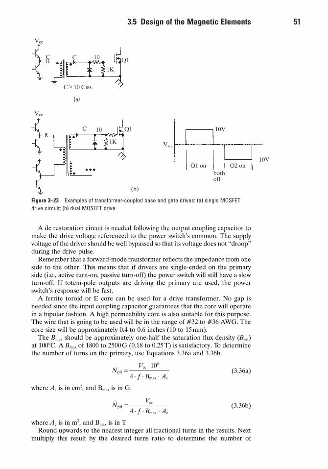
A dc restoration circuit is needed following the output coupling capacitor tomake the drive voltage referenced to the power switch’s common. The supplyvoltage of the driver should be well bypassed so that its voltage does not “droop”during the drive pulse.
Remember that a forward-mode transformer reflects the impedance from oneside to the other. This means that if drivers are single-ended on the primaryside (i.e., active turn-on, passive turn-off) the power switch will still have a slowturn-off. If totem-pole outputs are driving the primary are used, the powerswitch’s response will be fast.
A ferrite toroid or E core can be used for a drive transformer. No gap isneeded since the input coupling capacitor guarantees that the core will operatein a bipolar fashion. A high permeability core is also suitable for this purpose.The wire that is going to be used will be in the range of #32 to #36 AWG. Thecore size will be approximately 0.4 to 0.6 inches (10 to 15mm).
The Bmax should be approximately one-half the saturation flux density (Bsat)at 100°C. A Bmax of 1800 to 2500 G (0.18 to 0.25 T) is satisfactory. To determinethe number of turns on the primary, use Equations 3.36a and 3.36b.
(3.36a)
where Ac is in cm2, and Bmax is in G.
(3.36b)
where Ac is in m2, and Bmax is in T.Round upwards to the nearest integer all fractional turns in the results. Next
multiply this result by the desired turns ratio to determine the number of
NV
f B Apri
cc
c
=◊ ◊ ◊4 max
NV
f B Apri
cc
c
=◊
◊ ◊ ◊
10
4
8
max
3.5 Design of the Magnetic Elements 51
C C 10
1K
Q1
Vcc
C ≥ 10 Ciss
(a)
C 10
1K
Q1
Vsec
Q1 onbothoff
Q2 on-10V
10V
(b)
Vcc
Figure 3–23 Examples of transformer-coupled base and gate drives: (a) single MOSFETdrive circuit; (b) dual MOSFET drive.

secondary turns. The typical transformer will have a 1 :1 turns ratio for a powerMOSFET, and may be less that for a bipolar power transistor.
For dc input voltages that are more than 100VDC, a layer of Mylar tapeshould be placed between primary and the secondary(ies) and between any mul-tiple secondaries. One should not completely trust the insulation breakdownvoltage rating of the magnet wire since it could nick during the winding process.
3.5.9 Winding Techniques for Switchmode TransformersThe physical winding of switching power supply transformers is very important.It can make the difference between a switching power supply that is excellentand one that is noisy and poorly regulated. The design of switching power supplytransformers is much more critical than that of 50/60Hz transformers.
There are three major factors in the winding of the transformer:
1. Must the power supply meet any safety regulatory specifications?2. The windings should have tight electrical coupling.3. The leakage inductance of all the windings should be as low as possible.
Some of these factors fight one another so one should use the best compromisepractices.
Winding to meet safety regulationsIf the input voltage of the switching power supply is greater than 40V at thepeak, then the power supply comes under the regulation of one or more inter-national safety regulatory agencies. Many of these agencies mirror each other’ssafety limits, but the designer should still review the requirements for themarkets into which his or her company’s products are being sold. The Interna-tional Engineering Consortium (IEC) is the main standard-writing body, whosestandards have been adopted by all of the European Community safety agen-cies. The remaining safety agencies, such as Underwriters Laboratories (UL) inthe U.S., Canadian Standards Agency (CSA) in Canada, and VCCI in Japan,are working together to adopt a uniform set of safety standards based upon theIEC standard. This will allow one set of standards to be utilized all over theworld. Until the “harmonized” standards are adopted, there will be differencesamong countries around the world.
There are also differing standards between the markets in each of these coun-tries. For instance, the telecom market has vastly different safety requirementsthan the patient-contact medical market. So, it is important to determine thetarget market early in the product design process. These market differences willalso be included in the IEC standards harmonizing efforts.
The typical cores used in “off-line” or 90 to 265VAC input switching powersupplies are the E-E cores and their derivatives. These are bobbin-based coresand lend themselves for ease of manufacturing. The requirements of the safetyagencies are quite clear in the area of transformer construction. The creepage,or the distance across a surface between the input and output windings of atransformer, can be no less than 4mm. To accomplish this, the transformermaker places a 2mm tape build-up on both ends of the winding area in thebobbin and places the winding between the border tape. The border tape createsa 4mm total creepage distance between isolated windings. The typical IEC com-pliant transformer can be seen in Figure 3–24.
An insulating sleeve must also be placed around the wires as they exit fromthe bobbin because the wire passes within the 4mm space required by the regulations. The distance between the input and output pins must also be 4mm
52 Pulsewidth Modulated Switching Power Supplies

or more creepage distance apart from each other. This can also be accomplishedby having “fins” molded between the pins on the bobbin and other similar structures.
The creepage distance between the opposing phases of the input (betweenthe + and - dc and between the H1 and H2 (or hot and neutral) must be 3.2mm minimum.
The conductivity of a surface varies with the long-term pollution exposure inthe operating atmosphere and its average humidity. The previously mentionedcreepage spacings change for different applications, such as industrial, telecom,etc. The designer must refer to the appropriate specification.
The addition of tape, insulating sleeving, and pin spacing makes the finaltransformer much larger and higher in cost. This is because taping is a manualoperation and takes a significant amount of time to perform.
Another method to meet the safety specifications is the use of triple-insulatedwire for the secondary windings. Its use can reduce the transformer’s size andleakage inductance compared to the border-tape method. Triple-insulated wirehas three distinct, approved layers of insulation and it may be wound directlyin contact with the primary windings. Whether Mylar tape is needed in oraround the transformer depends upon the insulation system used in its con-struction. This type of transformer can be seen in Figure 3–25.
3.5 Design of the Magnetic Elements 53
1/2 Primary
Secondary
1/2 Primary
Bobbin
WI
2mmBorderTape
InsulatingSleeve
3 layers,6mil Mylar tape
Secondary
Primary
Bobbin
Triple InsulatedWire
3 layers, 6milMylar tape forexterior protection
Figure 3–24 IEC-compliant, interleaved, off-line transformer.
Figure 3–25 Off-line transformer using triple-insulated wire.

Winding for low leakage inductanceThere are choices and techniques that can minimize the amount of leakageinductance a winding will exhibit. Leakage inductance is a measurable amountof inductance that does not couple to the core or to another winding. It behaveslike a separate inductor in series with the winding lead. It is a parasitic elementthat causes spikes on the drain or collector of power switches and on the anodesof output diodes. That is because its flux cannot be loaded by the reflectedimpedances within the core.
An equation that estimates the amount of leakage inductance one mightexpect from a selected core and calculated winding is shown in Equation 3.37.
(3.37)
where K1 is equal to 3 for a simple primary and secondary winding, and isequal to 0.85 if the secondary winding is interleaved between twolayers of primary windings.
Lmt is the mean length of a turn around the bobbin for the wholewinding (in).
nx is the number of turns contained in the winding being analyzed.Wl is the length of the winding from end-to-end (in).
Tins is the thickness of the wire insulation (in).bw is the build (or thickness from the bobbin center-leg) of all the
windings of the completed transformer (in).The equation gives the major factors that affect the amount of leakage induc-
tance the winding will exhibit. A major factor that is under the control of thetransformer designer is the selection of a core that has a long center-leg. Thelonger the winding, the less leakage inductance will result. Keeping the numberof turns of a winding to its minimum also will help greatly, since its influence issquared. Additionally, the coupling of the primary winding to the secondarieshas a large affect on the primary leakage inductance. This is seen when the secondary is sandwiched, or interleaved, between two halves of the primarywinding.
Another annoying transformer parasitic element is the inter-turn capacitance.This resembles small capacitors distributed between turns throughout thewinding. Inter-turn capacitance is a problem in transformers with very high volt-ages across the primary winding. It is particularly a problem in off-line and highinput voltage switching power supplies. It is caused by two adjacent turns on thesame winding that reside at very different voltages. Equation 3.38 describes theenergy that is stored between only two turns within a winding. Of course thisenergy is multiplied many times by all of the turns that are next to one another,but the equation is informative as to the causes of the capacitance. This energyis released as spikes during the transition times.
(3.38)
where s is the space between the windings (m).d is the diameter of the wire (m).
The distributed capacitances can store a great amount of energy when layersof turns are wound back and forth on top of one another. At the ends, their
EV
s
d
stored( ) =ÊËÁ
ˆ¯
0 0194
2
2.
ln
LK L n
WT
bleak
mt xins
w=( )
+ÊËÁ
ˆ¯
12
1100 3
54 Pulsewidth Modulated Switching Power Supplies

voltages are very different and may even be close to the insulation breakdown.This will yield poor results. In Figure 3–26 three techniques are shown.
Progressive winding is when one to five turns wind across the first layer, thenthe wire is stepped back over that first layer and a second layer is placed on top.The most voltage that any turn sees is the number of turns in that progressivesegment. A sectioned bobbin can be used to separate equal winding segmentsof the primary winding so that the greatest voltage difference within a sectionwould be the input voltage divided by the number of sections.
The last technique is called Z-winding. After one layer is completed, the wireis run atop the bottom layer to the beginning side of the winding and then woundlike the first layer. Its performance falls between the zig-zag method first men-tioned (worst), and the sectioned bobbin and progressive techniques (best).
Low capacitance winding techniques also greatly reduces the dielectric stressof the wire insulation. This reduces the possibility of a arc jumping between twoadjacent windings due to insulation breakdown.
Winding the transformer for tight couplingTight primary-to-secondary and secondary-to-secondary coupling is the ulti-mate goal of the transformer designer. Poor coupling causes the power signalsto be delayed prior to reaching the output rectifier(s). The forward recoveryperiod of the output rectifier(s) is also added to this delay. This makes the windings essentially unloaded during the switching transitions, which createsvery large spikes on the windings due to the stored magnetization energy in thecore. Add the energy stored in the leakage inductance and the inter-turn capac-itance of the winding, and one has a problem.
Output cross regulation is affected by the amount of coupling between thesecondary windings. Cross-regulation is how the variation of the load on oneoutput affects the other outputs. It can be seen as the amount of “stiffness” inall of the outputs in a multiple output power supply in response to a change inload on any one output. Poor cross-regulation especially affects secondaries withwide differences in the turns ratios, that is, high voltage outputs mixed with lowvoltage outputs. There are two areas in which the designer can improve theoutput cross-regulation: the intrinsic cross-regulation that is designed into thetransformer through its construction techniques, and the electrical cross-regulation found in Section 3.9 (voltage feedback). Maximizing the performanceof both methods is usually needed for a reasonable power supply performance.
The first technique that enhances coupling between windings is twisted pairwinding. This occurs when two or more wires are twisted together and then
3.5 Design of the Magnetic Elements 55
+Vin
GND
(a) Straight WindingPoor
10
1 2 3 4 5
9 8 7 6GND +Vin
(b) “Progressive” WindingsVery Good
1 2 4 6 8 10
3 5 7 9 11 GND +Vin
(c) Sectioned BobbinGood
Figure 3–26 Winding technique for minimizing inter-turn capacitance.

wound onto the bobbin at the same time. For 24 though 28 gauge wires about3 twists per inch (or 1 twist per cm) is about right. Any tighter and the insula-tion could be damaged. This technique offers the best coupling by guarantee-ing that the wires always will be placed adjacent to one another. Even windingsof different lengths (turns) are helped by this technique. Having only a portionof the length twisted together, the coupling is improved.
Another winding technique is filar winding. This occurs when two or morewires are wound at the same time, but are not twisted. They rest next to theother wire(s) during most of the winding, but not all of it.
One wire product on the market is called Multiwire, with which two insulatedwires are bonded together, which accomplishes the same purpose. It is also moreeasily handled by the transformer maker.
Of course filar or twisted pair winding techniques cannot be used betweenthe primary and secondary when the peak primary voltage is more than 40 V.The safety agencies require that 3 layers of 1 mil thick Mylar tape (total thick-ness .006 inches with adhesive (0.167 mm)) be placed between the primary andsecondary windings for input voltages less than 260 VAC. This ruins the cou-pling between the two windings. One method to improve the primary-to-secondary coupling is to interleave the windings (see Figure 3–24). This tech-nique’s cost in labor is higher than simply having the secondary layered atop ofthe primary. Hence, it is recommended that the interleave technique be usedwhen the primary-to-secondary turns ratio exceeds 15–20 :1. This would includeswitching power supplies that operate at 240VAC or above and have a +5VDCoutput or below. Figure 3–27 shows the effects of interleaving on a 480VACinput, off-line flyback.
One can easily notice the difference in the spike energy between the two oscil-lographs. Typically, this energy is dissipated as heat within a clamp and/orsnubber across the primary winding.
Using transformer winding techniques that are effective, even though theymay be more costly to the transformer, can improve the overall performance ofthe power supply. This may save money for the whole power supply in the longrun.
3.6 The Design of the Output Stages
The output stage rectifies and filters the high frequency ac switching waveformcreated by the power switch(es). The nontransformer-isolated topologies (buck,boost, buck-boost, and sepic) rectify and filter the power switch-generated acsignal directly. The transformer-isolated topologies have a transformer betweenthe output stage and the power switches. The design of the output stage perhapshas the greatest effect on the efficiency of the power supply than any other stage,since the majority of the losses within the supply are seen in the output stage.
There are two basic types of output stage: those used in forward-mode con-verters and those used in boost-mode converters. The difference is the presenceof the output filter inductor between the rectifier and the output filter capaci-tor in the forward-mode output stage. Figure 3–28 shows the common outputstages.
For nontransformer-isolated switching power supply topologies, the outputrectifier is connected directly to the power switch and the output stage operatesin the half-wave mode. In transformer-isolated topologies, the output stage can
56 Pulsewidth Modulated Switching Power Supplies
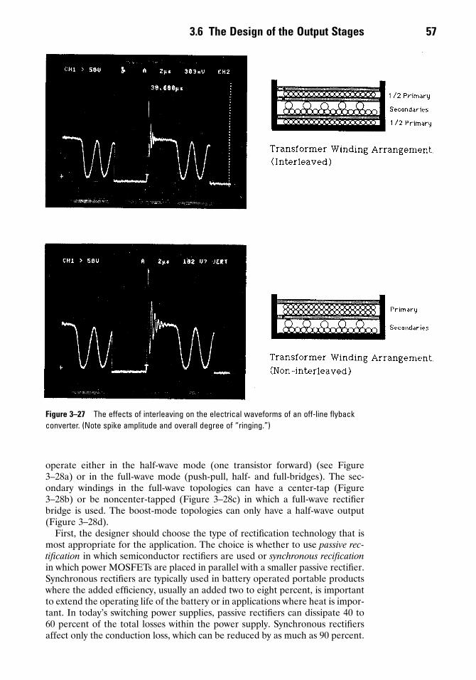
operate either in the half-wave mode (one transistor forward) (see Figure3–28a) or in the full-wave mode (push-pull, half- and full-bridges). The sec-ondary windings in the full-wave topologies can have a center-tap (Figure3–28b) or be noncenter-tapped (Figure 3–28c) in which a full-wave rectifierbridge is used. The boost-mode topologies can only have a half-wave output(Figure 3–28d).
First, the designer should choose the type of rectification technology that ismost appropriate for the application. The choice is whether to use passive rec-tification in which semiconductor rectifiers are used or synchronous recificationin which power MOSFETs are placed in parallel with a smaller passive rectifier.Synchronous rectifiers are typically used in battery operated portable productswhere the added efficiency, usually an added two to eight percent, is importantto extend the operating life of the battery or in applications where heat is impor-tant. In today’s switching power supplies, passive rectifiers can dissipate 40 to60 percent of the total losses within the power supply. Synchronous rectifiersaffect only the conduction loss, which can be reduced by as much as 90 percent.
3.6 The Design of the Output Stages 57
Figure 3–27 The effects of interleaving on the electrical waveforms of an off-line flybackconverter. (Note spike amplitude and overall degree of “ringing.”)

Their use, though, is restricted only to continuous-mode, forward-mode outputswhere the current flow can be guaranteed only in one direction. The designershould carefully consider the increase in efficiency verses the added cost of thedrive circuitry for the end application.
3.6.1 The Passive Output StageThe passive output stage is the traditional passive, semiconductor rectifier-based design. It is used for many applications that are not battery operated, andwhere switching power supply efficiencies of between 72 and 84 percent areacceptable. This would include many off-line applications where the heat gen-erated by the supply is easily handled within the power supply.
The choice of rectifier technology has a large affect on the overall efficiencyof power supply. There are common choices for rectifiers that tend to be depen-dent upon the output and input voltages. These two factors determine themaximum reverse voltage seen by the rectifier, which then dictates which typeof rectifier to use. The input voltage is seen by the output rectifier multipliedby the transformer turns ratio and the type of secondary winding used. Inoutputs that are full-wave rectified, the rectifiers only see the input voltage mul-tiplied by the secondary-to-primary turns ratio. Center-tapped secondariespresent twice the voltage seen by the full-wave rectified output. Equation 3.39gives the relationship for determining the minimum reverse blocking voltagerequired for a particular applications.
(3.39a)
(3.39b)
where k is 1 for full-wave secondary, and k is 2 for a center-tapped secondary.The ultrafast diode has a 0.8 to 1.1V forward voltage drop and exhibits a 35
V n n V Vr in out flyback> ( ) + ( )( )2 1 max
V k n n Vr in max forward> ( ) ( )( )2 1
58 Pulsewidth Modulated Switching Power Supplies
D LO
D CO Rload
transformer
Vr = (N2/N1) Vin(max) + Vout
(a)
D LO
D CO
D
Rload
transformer
Vr = 2(N2/N1) Vin(max) + Vout
(b)
D-Bridge
LO
D CO Rload
transformer
Vr = (N2/N1) Vin(max) + Vout
(c)
D
CO Rload
transformer
Vr = (N2/N1) Vin(max) + Vout
(d)
Figure 3–28 Output stages for forward and boost-mode converters: (a) half-wave forward-mode; (b) center-tapped forward-mode; (c) full-wave bridge forward-mode; (d) boost-mode.

to 85nS reverse recovery time. All P-N diodes have a significant reverse recov-ery time, where the ultrafast-type diode exhibits the shortest time. The reverserecovery time of a P-N diode is caused by the charge stored within the P-N junc-tion at the instant that the reverse voltage is applied to the diode. These minor-ity carriers must then reverse direction and require a finite period of time toreach the junction boundary. This is seen in the circuit as a current momentar-ily flowing in the reverse direction, when the voltage has already reached itsmaximum reverse bias. This equates to a very large instantaneous power loss(refer to Section 4.1). Ultrafast diodes are used in outpuis stages when thereverse voltage seen by the diode is too great for a schottky diode.
Schottky rectifiers have a 0.3 to 0.6V forward voltage drop and exhibit lessthan a 10nS reverse recovery characteristic. Schottky diodes are generally moredesirable, but have practical maximum reverse blocking voltages of about 40 to50V. This typically limits schottky diodes to those outputs of 15 VDC or less.Some schottky diodes have reverse blocking voltages as high as 200V but exhibita high junction capacitance characteristic that resembles the performance of aP-N reverse recovery characteristic.
Another difference between the ultrafast P-N and the schottky diode is thenature of the conduction characteristic of the diodes. The schottky diode has ahigher conduction resistance which makes its forward voltage drop increase withincreased forward current, as seen in Figure 3–29, curve A. This is caused bythe resistive nature of the bulk resistance of the drift region of the silicon. TheP-N-type diodes have a “flatter” forward conduction voltage characteristic moreindicative of the forward drop of the actual P-N junction, as seen in Figure 3–29,curve B.
The use of a full-wave bridge causes an added rectifier loss in series with theoutput current, which may lower overall efficiency. If the difference in reversevoltage is great enough to use Schottky diodes instead of one P-N diode, usuallythe advantage falls to the Schottky diodes. The advantages would be a slightlysmaller secondary winding and better reverse recovery performance.
3.6 The Design of the Output Stages 59
ASchottky
BP–N
knee V
1.0 V
Forward Voltage (V)
rated
0.5ratedFo
rwar
d C
urre
nt (
A)
Figure 3–29 Forward conduction voltage characteristic of the Schottky versus the ultrafastdiode.

3.6.2 Active Output Stages (Synchronous Rectifiers)For those applications where high efficiency is important, synchronous rectifi-cation may be used on the higher current (power) outputs. Synchronous recti-fier circuits are much more complicated than the passive 2-leaded rectifiercircuits. These are power MOSFETs, which are utilized in the reverse conduc-tion direction where the anti-parallel intrinsic diode conducts. The MOSFET isturned on whenever the rectifier is required to conduct, thus reducing theforward voltage drop to less than 0.1 V. Synchronous rectifiers can be used onlywhen the diode current flows in the forward direction, that is in continuous-mode forward converters.
Figure 3–30 shows the common ways synchronous rectifiers are employedwithin switching power supplies.
A small Schottky rectifier with a current rating of about 20 to 30 percent ofthe MOSFET current rating (ID) is placed in parallel with the MOSFET’s intrin-sic P-N diode. The parallel schottky diode is used to prevent the MOSFET’sintrinsic P-N diode from conducting. If it were allowed to conduct, it wouldexhibit both a higher forward voltage drop and its reverse recovery character-istic. Both can degrade its efficiency of the supply by one to two percent.
60 Pulsewidth Modulated Switching Power Supplies
Vin
Drivefrom IC
+ Vout
Co
-
(a)
Primary
Lo
Co
+ Vout
-
(b)
VG
ControlIC
1 : 1
GateX fmr
C RG
1K
C > 10Ciss
(c)
Figure 3–30 Common synchronous rectifier circuits: (a) nonisolated; (b) self-driven; (c) transformer-coupled.
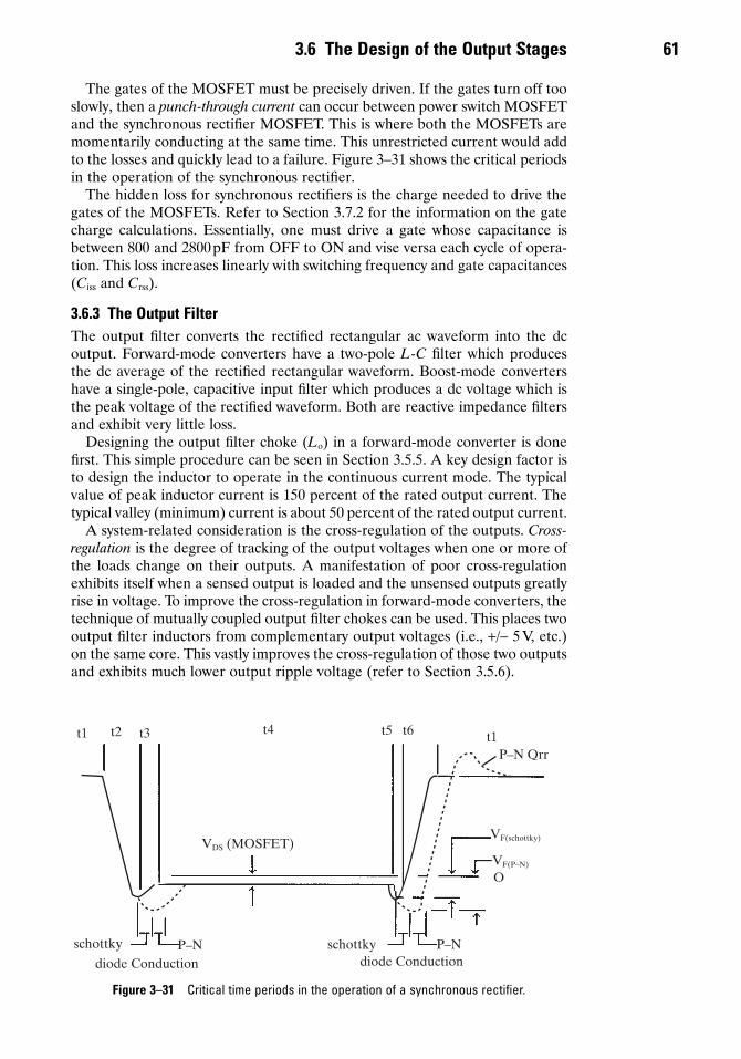
The gates of the MOSFET must be precisely driven. If the gates turn off tooslowly, then a punch-through current can occur between power switch MOSFETand the synchronous rectifier MOSFET. This is where both the MOSFETs aremomentarily conducting at the same time. This unrestricted current would addto the losses and quickly lead to a failure. Figure 3–31 shows the critical periodsin the operation of the synchronous rectifier.
The hidden loss for synchronous rectifiers is the charge needed to drive thegates of the MOSFETs. Refer to Section 3.7.2 for the information on the gatecharge calculations. Essentially, one must drive a gate whose capacitance isbetween 800 and 2800 pF from OFF to ON and vise versa each cycle of opera-tion. This loss increases linearly with switching frequency and gate capacitances(Ciss and Crss).
3.6.3 The Output FilterThe output filter converts the rectified rectangular ac waveform into the dcoutput. Forward-mode converters have a two-pole L-C filter which producesthe dc average of the rectified rectangular waveform. Boost-mode convertershave a single-pole, capacitive input filter which produces a dc voltage which isthe peak voltage of the rectified waveform. Both are reactive impedance filtersand exhibit very little loss.
Designing the output filter choke (Lo) in a forward-mode converter is donefirst. This simple procedure can be seen in Section 3.5.5. A key design factor isto design the inductor to operate in the continuous current mode. The typicalvalue of peak inductor current is 150 percent of the rated output current. Thetypical valley (minimum) current is about 50 percent of the rated output current.
A system-related consideration is the cross-regulation of the outputs. Cross-regulation is the degree of tracking of the output voltages when one or more ofthe loads change on their outputs. A manifestation of poor cross-regulationexhibits itself when a sensed output is loaded and the unsensed outputs greatlyrise in voltage. To improve the cross-regulation in forward-mode converters, thetechnique of mutually coupled output filter chokes can be used. This places twooutput filter inductors from complementary output voltages (i.e., +/- 5V, etc.)on the same core. This vastly improves the cross-regulation of those two outputsand exhibits much lower output ripple voltage (refer to Section 3.5.6).
3.6 The Design of the Output Stages 61
t1 t2 t3 t4 t5 t6 t1P–N Qrr
VF(schottky)
VF(P–N)
P–Nschottkydiode Conduction
VDS (MOSFET)
P–Nschottky
diode Conduction
O
Figure 3–31 Critical time periods in the operation of a synchronous rectifier.

The calculation of the output filter capacitor (Co) is the same for both theforward-mode and boost-mode output stages. Its value is simply determined bydeciding how much peak-to-peak output ripple voltage one desires on theoutput voltage. Output ripple voltage is a small triangular ac waveform that ridesatop the dc output voltage. For forward-mode converters, one can expect a typical output ripple voltage of 30mVp-p. In boost-mode outputs a value of 150mVp-p is typical. If ripple-sensitive circuits are on a particular output, thedesigner should consider the addition of a dc filter stage following the outputfilter capacitor (refer to Section 3.5.7). To calculate the value of the output filtercapacitor one executes Equation 3.40.
(3.40)
where Iout is the rated output current for that output (amps).∂(min) is the smallest estimated duty cycle at high input line and
at light load (an estimate of 0.3 is good).Vripple(pk-pk) is the desired peak-to-peak output ripple voltage (volts).
Especially within flyback-mode converters, the choice of the proper capaci-tor is extremely important. This is because the flyback-mode converters have noinductive impedance between the rectifier and themselves. This allows very highinstantaneous values of current to enter and exit the capacitor. This high accurrent flows through the ESR (equivalent series resistance) and ESL (equivalentseries inductance) of the capacitor. The ESR causes the capacitor to get hot,shortens its life, and adds additional ripple voltage to the theoretical value usedin Equation 3.40. ESL adds sharp step functions and spikes to the theoreticalripple voltage waveform. Tantalum capacitors are better than aluminum elec-trolytic capacitors in regards to superior ESR and ESL properties. In boost-mode converters, the approximate peak-to-peak ac ripple currents entering thefilter capacitor is given by using Equation 3.41. Converting this peak-to-peakvalue to RMS, given by capacitor manufacturers, can be a difficult exercise inmathematics. As an approximation use about 33 percent of the peak-to-peakvalue as the RMS.
(3.41)
Capacitor manufacturers have only begun to specify the use of their capaci-tors in high frequency switching power supplies. One must use care whenreviewing capacitors for use in one’s power supply. The ESR should be speci-fied at a frequency greater than 1kHz.
To properly design the capacitance for the output stage, one should placeenough capacitors in parallel so that each capacitor operates at about 70 to 80percent of its maximum ripple current rating. The sum of the capacitors shouldequal the final calculated value, but each capacitor should have the value ofCtot/n, where n is the number of capacitors in parallel.
Ultimately, the designer must try-out the final design and check the outputripple voltage and the temperature rise of each capacitor.
One last factor is the physical layout of the output stage when more than oneoutput filter capacitor is used. The capacitors should be located radially sym-metric from the output rectifier, and the printed circuit traces for the rectifiedvoltage and the grounds should be of similar trace-widths and lengths. Any dis-similarity of these traces causes more series resistance and inductance to the
I
Iripple pk pk
out av
min
-( )( )ª
2
∂
CI
f Vout min
out max
ripple pk pk
( )( ) ( )
-( )=
◊ -( )◊
1 ∂ min
62 Pulsewidth Modulated Switching Power Supplies

remote capacitor. This makes the closest capacitor experience more of theripple current and therefore get hotter. PCB traces also add to the ESR andESL values to the capacitors. Refer to Section 3.14 for a more in-depth discus-sion on PC design.
A high frequency capacitor could also be placed in parallel with the largercapacitors. This is because the aluminum electrolytic and tantalum capacitorscannot absorb the very high frequency current components being presented tothem. A .01 or .1 mF ceramic capacitor is well suited for this purpose.
3.7 Designing the Power Switch and Driver Section
The main purpose behind the power switch section is to convert the dc inputvoltage to a pulsewidth modulated ac voltage. The following stages can use atransformer to step-up or step-down the ac waveform, and finally the outputstage converts the ac into the dc output(s). To accomplish the dc-to-ac conver-sion, the power switch operates only in the saturated and cutoff states. Thismakes the losses as low as possible.
There are two major types of power switches used today: the bipolar powertransistor (BJT) and the power MOSFET. The IGBT (integrated gate bipolartransistor) is used in the higher power industrial applications, such as >>1kWpower supplies and electronic motor drives. The IBGT has a slower turn-offthan does the MOSFET, so it is typically used for switching frequencies of lessthan 20kHz.
3.7.1 The Bipolar Power Transistor Drive CircuitsThe bipolar power transistor is a current driven device. To guarantee a “switch-like” operation, it must operate close or within its saturated state. For this tooccur, the “on” base current must satisfy (also refer to Figure 3–29).
(3.42)
where IB is “on” base drive current.IC(max) is the maximum anticipated collector current.
hFE is the minimum specified dc gain of the transistor.There are two types of base drive schemes. Fixed base drive, shown in Figure
3–33, drives the transistor into saturation over the entire conduction period.Since the collector current is almost always less than the maximum expectedvalue, the transistor is nearly always being overdriven. Driving the transistordeep into saturation results in a slow turn-off time. The parameter storage time(tS) is the time delay between the “off” signal to the base and when the collec-tor begins to turn off. During this time the collector-to-emitter voltage contin-ues to maintain a saturated voltage level. Although it is not a loss, it does requirea shortening of the maximum duty cycle the power supply can use. The drivecircuit should provide fast transitions in the base current (on and off) and drawthe base voltage slightly negative.
The design philosophy behind the fixed-base drive circuit is to draw currentfrom a relatively low voltage source (3 to 5V) which is usually provided by anauxiliary winding on the power transformer. The resistor directly in series withthe base (R2 as shown in Figure 3–33) should be on the order of 100 ohms. Its
II
hB
C max
FE min
≥ ( )
( )
3.7 Designing the Power Switch and Driver Section 63

purpose is to limit the dc current entering the base during turn on and turn off.A small capacitor on the order of 100 pF should be placed in parallel with thisseries resistor (R2). This is called a base speed-up capacitor, which provides arapid positive and negative surge of current during the turn-on and turn-offtransitions of the transistor. This reduces switching times and reduces the threatof second breakdown and current crowding. The resistor on the collector of thebase driver transistor (R1 as shown in Figure 3–33) further controls the on-state
64 Pulsewidth Modulated Switching Power Supplies
IB
IC
+
VCE
–
+
VBE
–Symbol
BRb
CCE VBE
hFE·IbC
E
Approximate Equivalent Circuit
BaseCurrent
IB1
IB2
time
timetf
tS
Vsat
tr
Collector-to-emitterVoltage
CollectorCurrent
Ipk
timeTurn-off loss,CurrentCrowding Period
Saturation LossTurn-onLoss, Second
Breakdown Period
Figure 3–32 Waveforms for a bipolar power transistor within a PWM switching powersupply.

base drive current. The base voltage should be checked with an oscilloscope andshould go slightly negative during the turn-off transition, but should not exceedthe base-emitter avalanche voltage rating (<5V).
The second scheme, shown in Figure 3–34, is called proportional base driveand always drives the transistor at or just below the transistor’s saturation state.The collector-emitter voltage is higher than with fixed base drive, but the tran-sistor can now switch in about 100 to 200nS. This is five to ten times faster thanwith fixed base drive. In practice, though, the fixed base drive scheme is used inthe majority of low- to medium-power, low-cost applications. Proportional basedrive is used for the higher-power applications.
3.7 Designing the Power Switch and Driver Section 65
Vbb
CfR1
1000pF100pF
IB
T
Q2
R3Q1R2
1K
Control IC
Drive GNDPower Ground
(a)
Q1 – 2N3904 or equivalent NPN
R3 ª 62 W, 1/4 W
PD(R1) ª IB·R12
R2 ª 100 W, PD ª IB·R22
Vcc – 1.0 VR1 ª
IB
– R2
Q
R3 ª 64 W, 1/4 W
R1 & R2 see above
Vbb
R1 C1
100pF
T
R2R3
Power GroundControl IC
(b)
Vbb
C1100pF
R1T2
n1 n2 R2 R3
T1
Q
Power GroundControl IC
(c)
R3 ª 62 W, 1/4 W
R2 – see above
VCCR1 ª(N2/N1)·IB
VccPD(R1) ª R1
2
Figure 3–33 Fixed base drive circuits: (a) quasi-totem-pole drive; (b) totem-pole drive; (c) transformer-coupled drive.

The last consideration is from which voltage to draw the base current. Sincethe base-emitter junction resembles a forward-biased diode, the maximum VBE
is 0.7 to 1.0V. Ideally, a voltage source of 2.5 to 4.0V is sufficient. If the basedrive voltage source is too high, there will be a significant loss associated withdriving the base.
In the initial breadboard, the voltage and current waveforms associated withthe power transistor must be carefully scrutinized and it must be verified thatthey do not exceed the SOA limits. This is also the time to modify any valuesthat enhance its switching characteristics, since it represents about 40 percentof the supply’s entire losses. The drive schemes shown in Figures 3–33 and 3–34are the common approaches to driving the bipolar transistor and will give thedesigner a very good staring point.
3.7.2 The Power MOSFET Power SwitchThe power MOSFET is the most common choice as a power switch. Its cost andsaturation loss are comparable to the bipolar transistor in most applications andit switches five to ten times faster. It is also easier to use in a design.
The MOSFET is a voltage-controlled current source. To drive a MOSFETinto saturation, enough voltage must be applied between the gate-source ter-minals in order to pass more than the maximum expected drain current. Therelationship between gate-to-source voltage and drain current is called transcon-ductance or gm. Power MOSFETs fall typically into two categories: standardMOSFETs, which must have about 8 to10v Vgs to guarantee full-rated drain
66 Pulsewidth Modulated Switching Power Supplies
Vbb
R1 Cf
D2+
VCE
–
QD1 D3+
VBE–100pF
R2
D4 R3
Power Ground
Control IC
(a)
D1, D3, D4 – 1N4148
D2 Ultra Fast Recovery DiodesIF ª IB, VR(D2) > VCE
R3 ª 62 W, 1/4 W
R2 ª 100 W, PD ª IB·R22
PD(R1) ª IB·R12
Vcc – 1.0 VR1 ª
IB
– R2
Vbb
R1 C1100pF
T1
QR3R2n2n1
Control ICPower Ground
(b)
R3 ª 62 W, 1/4 W
VccR1 ª(N2/N1)·IB
R2 approx. 100 W
T2
Figure 3–34 Proportional base drive circuits: (a) the Baker clamp; (b) transformer-coupledproportional base drive.

current, and logic-level MOSFETs, in which only 4.0 to 4.5V is needed. Logic-level MOSFETs typically have low drain-to-source voltage ratings (<60V).
MOSFETs can switch very quickly, typically from 40 to 80 nS is common. Todrive the MOSFET this fast, one must consider the intrinsic parasitic capaci-tors which exist in all power MOSFETs (see Figure 3–35).
These capacitances are specified in each power MOSFET datasheet and arevery important. Coss, or drain-to-source capacitance, is considered in the drainloads, but does not directly enter into the drive design. The Ciss and Crss havedirect and calculable effects upon the switching performance of the MOSFET.Figure 3–36 shows the gate and drain waveforms of a typical N-channelMOSFET switching cycle.
The plateau in the gate drive voltage signal is caused by the opposing transi-tion in the drain-to-source signal being coupled into the gate node through the
3.7 Designing the Power Switch and Driver Section 67
Drain
Crss
GateCiss
Source
Coss
Figure 3–35 The symbol of a power MOSFET with the parasitic capacitances.
turn-on
t3t2t1
0
VGS
Vth
Vpl
VDR
t3
turn-off
t2t1
0
+0–
IG
VDS
Figure 3–36 The MOSFET waveforms.

miller capacitor (Crss). During this period, a large impulse is seen in the gatedrive current. This plateau occurs at a voltage slightly higher than the rated gatethreshold voltage and is VTH + ID/gm. The value of the plateau voltage can alsobe determined by using the transfer function graph provided in every MOSFETdata sheet (see Figure 3–37). For an inaccurate estimation, the threshold voltagecan be used. The MOSFET datasheets provide the graphs seen in Figure 3–37.
These capacitances cause delays in the switching performance of theMOSFET. The drive circuits should be able to drive capacitive loads. First, theamount of charge required to transition the gate through each voltage level mustbe determined. Figure 3–37 yields this information when one subtracts the differences in gate drive voltage operating points from one another. The switch-ing delay can be calculated from Equations 3.43 through 3.50.
Turn-on delays:
CMOS Bipolar
Turn-off Delay t(1) ª (3.43)
Risetime t(2) – (3.44)Q
V V
t2 eff OH
OH p1
R( ) ( )
-
Q
I
t2
OH
( )
Q
V
t1 eff OH
OH
R( ) ( )Q
I
t1
OH
( )
68 Pulsewidth Modulated Switching Power Supplies
50
40
30
20
10
0
ID D
rain
Cur
rent
(A
)
2 3 4 5
VDS=5V Ta=–55C25C
125C
VGS Gate-to-Source Voltage (V)
5000
3000
1000
500
2000.1 0.3
Cap
acit
ance
(pF
)
1 3 10 30
Drain-to-Source Voltage (V)
Ciss
Coss
Crss
10
8
6
4
2
0VD
S G
ate-
Sour
ce V
olta
ge (
V)
Id = 11A VDS=5V10V
15V
0 10 20 30 40 50 60
Qg, Gate Charge (nC)
Figure 3–37 Representative datasheet curves for a MOSFET.

t(3) – (3.45)
(3.46)
Turn-off delays:
COMS Bipolar
Turn-off Delay t(3) – (3.47)
Falltime t(2) – (3.48)
t(1) – (3.49)
(3.50)
Bipolar-based drivers are more able to source the current surges needed bythe MOSFET gate than CMOS-based drivers, which act more like a current-limited source and sink. Speed is typically controlled by placing a resistor inseries between the driver and the gate. In switching power supplies, when rapidswitching is required, a resistor of over 27ohms is not advisable, since its switch-ing speed would drop and its switching loss would rise significantly. Larger seriesgate resistors would create short periods of oscillation when the drain voltageis transitioning.
3.7.3 The IGBT as a Power SwitchThe IGBT is a silicon hybrid composed of a power MOSFET on the gate ter-minal and an “unlatchable” SCR between the collector and emitter terminals.Its internal schematic can be seen in Figure 3–39.
The advantages of IGBTs over MOSFET devices are the savings in silicon diearea and its bipolar collector current characteristics. It also has two disadvan-tages: higher saturation voltage due to two series P-N junctions, and the factthat IGBTs can have a long turn-off “tail,” which adds to the switching loss. The“tail” loss has limited the switching frequencies to less than 20kHz. This hasmade it ideal for industrial electronic motor drives where the switching fre-quency is just beyond the human audio range.
IGBTs have been the target of much research by semiconductor companiesand the tail time has been shortened significantly. Originally, the tail time wasabout 5uS; now the tail time is about 100 nS and is improving. The saturationvoltage has also been improving from approximately 4 V to less than 2V.Although this is a problem for low-voltage dc-dc converters, it has a great dealof appeal for off-line and industrial, high-power converters. As a personal judg-ment, I would consider IGBTs for those converters with input voltages greaterthan 220VAC and 1 KW.
Reff OHDR OH
OL
( ) --V V
I
Q
V V
t1 eff OL
OL p1
R( ) ( )
-Q
I
t1
OL
( )
Q
V V
t2 eff OL
OL p1
R( ) ( )
-
Q
I
t2
OL
( )
Q
V V
t2 eff OL
OH p1
R( ) ( )
-Q
I
t3
OL
( )
Reff OLOL
OL
( ) -V
I
Q
V V
t3 eff OH
OH p1
R( ) ( )
-
Q
I
t3
OH
( )
3.7 Designing the Power Switch and Driver Section 69

Driving the IGBT is identical to the MOSFET. It has similar gate driving char-acteristics and a MOSFET driver IC works very well with an IGBT.
3.8 Selecting the Controller IC
Today, one has many choices in the area of controller-integrated circuits. Onemust decide early in the design process how much functionality and integration
70 Pulsewidth Modulated Switching Power Supplies
VG Load
Ron
(a)
VG
Load
Roff
(b)
LoadVGVG
(c)
Load
(d)
VG
C
C RG
1K
1:1
C> 10 Ciss
(e)
T
Figure 3–38 MOSFET drive circuits: (a) passive turn-on; (b) passive turn-off; (c) bipolartotem-pole; (d) MOS totem-pole; (e) transformer-isolated drive.
Collector
Gate
EmitterSCR
Figure 3–39 The IGBT.

is desired in the IC, such as whether the power switch should be inside the IC,the high voltage start-up circuit, soft start circuit, synchronization circuits, etc.This is driven by the application and the extra functions that are desired.
Extreme caution must be practiced reviewing candidate ICs. The first pageof the data sheet does not always completely describe the IC. Subtle factorsinvolving the method of control, how the output drivers are to be used, and howthe protection circuit operates must be further investigated. This requirescareful review of the internal IC and applications schematics. An example whereconfusion creeps in is the newer generations of buck controller ICs for less than3.3V outputs. These ICs are designed to operate from a higher supply voltagethan their input power line and drive the MOSFETs at a very low voltage level.The traditional buck controller operates from its input voltage and drives theMOSFET from the input voltage. One cannot differentiate these two ICs apartfrom the first page of the datasheet and it is even more difficult to tell themapart if they are presented as a result of a search on a supplier’s website. Thiscould cost you valuable time.
Today, more than ever, the new control ICs are targeted narrow applicationniches. This typically includes removing as many pins as possible from thepackage to minimize external circuits. This severely limits the flexibility of anIC. This makes the selection process even more important.
3.8.1 Short Overview of Switching Power Supply ControlThis short overview may be redundant from the earlier part of this chapter, butit is appropriate. The primary purpose of the controller is to maintain a con-stant output voltage for a large range of load currents. A negative feedback loopis used for this purpose. All power supply controllers, both linear and switch-ing, sense the output voltage. The rated output voltage is reduced to the levelof a voltage reference somewhere within the control IC. This feedback voltageis placed into the inverting input of a high-gain op amp called the voltage erroramplifier. The reference voltage is placed into the non-inverting input of thesame op amp. The output of the amplifier represents a greatly amplified versionof the difference between the reference and the output voltage. This outputvoltage is called the error voltage. This error voltage is then used to control theamount of energy the power supply wants to pass to the load. It can have a positive value, indicating that the output is too low and the power supply needsto supply more energy to the output. Conversely, a negative value indicates thatthe output is too high and the thruput energy should be reduced.
Current is typically sensed so that the power supply does not exceed its powerratings. There are two methods of measuring current: average output currentand instantaneous current. Average current circuits operate in a very similarmanner to the voltage feedback loop described previously. Current is typicallymeasured as a voltage across a resistor placed in series with the current to bemeasured. This voltage is amplified or used in its very small value. This voltageis then placed into the inverting pin of an operational amplifier and a referencevoltage representing the desired maximum value of the output. When thecurrent gets too high, the current error voltage swings from positive to negative,indicating that the output current has exceeded the desired maximum amount.This signal can be used to override the voltage error signal and reduce theenergy thruput of the power supply.
Instantaneous current sensing is used to protect the power semiconductors. Acurrent sensing resistor is placed in the power switch current path and its voltagerepresents the instantaneous current flowing through the power device. This
3.8 Selecting the Controller IC 71

voltage is then taken to a very fast analog comparator where if a predeterminedvoltage is ever exceeded, the power device is instantly turned off. This offersvery nice protection of the power device.
3.8.2 Selecting the Optimum Control MethodThe selection of the control IC is very important. If the wrong choice is made,it could result in supply instability and waste valuable time. The designer shouldunderstand the subtle difference between the various forms of control. Ingeneral, forward-mode topologies usually have voltage-mode controllers, andboost-mode topologies usually have current-mode control. This is not a rock-solid rule since every method of control can be used for every topology, withmixed results.
Voltage-mode controlThis method of control can be seen in Figure 3–40. The important trait ofvoltage-mode control is that the error voltage is placed into a PWM compara-tor and compared against a clock generated sawtooth waveform. As the errorvoltage rises and falls the pulsewidth of the output signal increases anddecreases. To identify a voltage-mode control IC, look for a capacitor R-C oscil-lator and see if the capacitor sawtooth voltage goes to a comparator with the errorvoltage.
There are two versions of overcurrent protection on voltage-mode controlICs. The older version is average current foldback. Here, the output current is
72 Pulsewidth Modulated Switching Power Supplies
Table 3–6 PWM Control MethodsControl Method Optimum Topology Issues
Voltage-mode with Forward-mode OC foldback slow, couldaverage OC foldback cause power switch
failuresVoltage-mode with Forward-mode Very good OC protection;pulse-to-pulse OC usually hi-side currentlimiting sensingHysteretic current- Forward- and Heavily patented;mode boost-mode few control ICsCurrent-mode, Boost Very good OC protection;turn-on with clock many ICs; typically
GND-driven SW
Quasi-Resonant and Resonant-transition Control MethodsControl Method Optimum Topology Issues
Constant off-time Zero voltage Variable frequencyswitching QR High frequency limit
neededConstant on-time Zero current Variable frequency
switching QR Low frequency limitneeded
Phase modulated PWM forward- Fixed frequencymode full bridge

Figure 3–40 Voltage-mode control with average output and pulse-to-pulse current limiting.
3.8 Selecting the Controller IC 73
OSC.
VCC
Charge
DischargeCt
Volt. Comp.
VFB +
Cur.Comp.
Voc
Vref
Iout
(lavOC)orISW
(P-POC)
–
V Error Amp.
+
–
–
+
+
–VSS
Steering PulsewidthComparator
AverageOC
+
–
OutputGatingLogic
V
Pulse-to-Pulse OCRCS
sensed with a resistor in series with the load. The current signal may be ampli-fied and inputted to a compensated current error amplifier. The current ampli-fier then senses when the output current approaches its preset limit and willoverride the voltage error amplifier and limit the current, if the current attemptsto grow larger. Average current foldback has one inherent flaw when used byitself as an overcurrent protection, its response is too slow to prevent damageto the power switch if a sudden short circuit is applied to its output and cannotsense when the magnetic elements are entering the saturated state. These cancreate exponential currents in a matter of several microseconds and destroy thepower switch.
The second method of overcurrent protection is pulse-to-pulse overcurrent pro-tection. This method guarantees a maximum safe power switch current. Acurrent sensing element (resistor or current transformer) is placed in series withthe power switch(es). It views the instantaneous current flowing through thepower switch and will instantly cutoff the power switch if a preset instantaneouscurrent limit is exceeded. This circuit must be very fast and will protect thepower switch from all forms of instantaneous overcurrents including core satu-ration. It is not a form of current-mode control since this protection limit is fixedand not influenced by external parameters.
One last form of voltage-mode control is very rudimentary. It could be calledhysteretic voltage-mode. In this form of control, a fixed frequency oscillator isgated “ON” only when the output voltage has fallen to below a limit dictatedby the voltage feedback loop. It is sometimes called “hiccup-mode” because thepower switch occasionally bursts on and then returns to a constant off state.

There are a few control ICs and integrated switching power supply ICs that havethis mode of control. It produces a fixed amount of ripple on the output voltagewhich varies in frequency in proportion to the load current.
Current-mode controlCurrent-mode control is best used in topologies where the linear slopes withinthe current waveforms are higher. This would be the boost-mode topologiessuch as boost, buck-boost, and flyback.
Current-mode methods control the peak (and sometimes the minimum)current excursion points flowing though the power switch. This equates to theexcursions of the flux density within the magnetic core. Essentially the magneticbehavior of the core is being regulated. The most common form of current-mode is “turn-on with clock.” This is when a fixed frequency oscillator sets aflip-flop and a high speed current comparator resets the flip-flop. The “1” stateof the flip-flop is when the power switch is conducting.
The threshold for the current comparator is set by the output of the voltageerror amplifier. If the voltage error amplifier indicates that the output voltageis too low, then the current threshold is raised to allow more energy to reachthe load. The converse is true too.
Current mode control has an inherent overcurrent protection. The high-speed current comparator provides pulse-to-pulse current limiting. This formof protection is a constant power form of overload protection (see Section 3.11).This form of protection folds back the current and voltage to maintain a con-stant power into the load. This may not be optimum for all products, especiallywhere the typical failures slowly increase the failure current. Another form ofoverload protection can also be placed in the circuit.
Another form current-mode control is called hysteretic current-mode control.Here both the peak and the valley currents are controlled. This is obviouslybetter for continuous-mode forward for boost converters. It is somewhat com-plicated to set-up, but it does offer very fast response times. It is not a verycommon method of control and its frequency varies.
Other modes of controlSome IC makers today take many liberties in creating new modes of control orswitching control methods at some operating points to enhance the overall effi-ciency of the target power supply. This practice can be confusing and may notoperate in all applications other than the application it was design. For example,some buck controller ICs will allow the inductor to enter the discontinuous-mode, by dropping the frequency of operation. The feedback loop stability maychange, so they use some obscure control method to compensate for the anti-cipated instability.
Voltage Hysteretic Control. This is what people used to call “hiccup-mode.” Asimple comparator is used to view the output voltage. If the voltage falls belowa certain limit, the PWM loop turns on for a period of time until this limit issurpassed (plus some hysteresis voltage). It guarantees that the output voltageripple is equal to or greater than the amount of hysteresis voltage in the controlcircuit.
Variable Frequency Control. At light loads, fixed frequency control methodsloose efficiency because of the fixed switching losses. Some controllers will
74 Pulsewidth Modulated Switching Power Supplies

switch to a variable frequency clock at light loads, but retain the same methodof control.
Summary. Be very careful in selecting a control IC for your application!
3.9 Designing the Voltage Feedback Circuit
The only function of the voltage feedback loop is to hold the output voltage(s)at a constant value. Complications arise in areas such as transient load response,accuracy of the output(s), multiple outputs, and isolated outputs. All of theseindividually can be nightmares for the designer, but if the design approachesare understood then each factor can easily be satisfactorily addressed.
The heart of the voltage feedback loop is a high-gain operational amplifierwhich is called an error amplifier, which is nothing more than a high-gain ampli-fier that amplifies the difference between two voltages and creates an errorvoltage. In power supplies, one of these voltages is a reference voltage and theother represents the level of the output voltage. The output voltage is typicallydivided down to the voltage of the voltage reference prior to being presentedto the error amplifier. This creates a “zero error” point for the error amplifier.If the output deviates from this “ideal” value, the error voltage output of theamplifier changes significantly. This error voltage then is used by the powersupply to provide a correction to the pulsewidth to bring the output voltage backto its ideal value.
3.9 Designing the Voltage Feedback Circuit 75
VFB
VCC
OSC.
Ct Discharge
VoltComp.
V Error Amp.
+
–Vref
–
+
–
+
ISW RCS
VSS
IpkVerror
Verror
S
R
Q
CurrentComparator
OutputGatingLogic
Output
SWon
CLK Ipk
–
+
Figure 3–41 Turn-on with clock current-mode control.

The major design issues surrounding the error amplifier are that it shouldhave a high gain at dc which promotes good output load regulation and have agood high frequency response which promotes good transient load response.Output load regulation is how closely the output voltage is maintained with achange in the load of the sensed output. Transient response is how quickly theoutput voltage returns to its rated value after a step response to the load hasoccurred. These issues come under the area of feedback loop compensation,which is covered in detail in Appendix B.
An example of an elementary voltage feedback application is the nonisolated,single-output switching power supply. If we neglect the error amplifier com-pensation, then the design is quite simple. Let us examine a situation where a5V output is regulated and a 2.5V reference is provided within the control IC.This can be seen in Figure 3–43.
To begin the process, one decides how much sense current is to be drawnthrough the output voltage resistor divider. For the sake of reasonable valuesto be calculated for the error amplifier compensation values, resistance valuesin the range of 1.5 to 15 K should be used in the upper leg of the resistor divider.Let us use a sense current of 1mA as the resistor divider sense current. Thismakes the lower resistor in the divider (R1)
The accuracy of the output voltage is directly affected by the tolerance of theresistors used in the voltage divider and the accuracy of the voltage reference.All of the tolerances add to determine the resulting accuracy. That is, if two onepercent resistors are used within the divider, and a two percent reference wasalso used, a four percent accuracy can then be expected in the final outputvoltage. Some additional error is introduced by the input offset voltage of theamplifier. Its error contribution is the value offset voltage divided by the divideratio of the resistor divider. So, if an amplifier has a 10mV maximum offset
R1 2 5 001 2 5= =. . .V A K
76 Pulsewidth Modulated Switching Power Supplies
VFB
VoltComp.
V Error Amp.
–
++
–Vref
IL
Rcs IPK
Imin
VSS
–
+
–
+
Imin CurrentComparator
OutputGatingLogic
OutputS
R
Q
IPK Current
Comparator
Figure 3–42 Example of hysteretic current-mode controller.

voltage in this design example, one can expect a output voltage error of 20mVthat will drift with temperature.
Continuing the design example, let us use the closest 1 percent resistor value-2.49K. This makes the actual sense current
The upper resistor in the resistor divider (R2) is then
That completes its set-up. Later, the compensation around the amplifier needsto be done to set the dc gain and the bandwidth performance.
If the power supply has multiple outputs, then cross-regulation of the outputsis a concern. Usually only one or several outputs can be sensed by the voltageerror amplifier. The unsensed outputs can then only be regulated by the intrin-sic cross-regulation abilities of the transformer and/or output filters. This canbe quite poor, meaning that a change in the sensed output’s load causes theunsensed outputs to change significantly. Conversely, if an unsensed output’sload is changed, it is not adequately sensed through the coupling in the trans-former to the sensed output, to have it exhibit good regulation.
To greatly improve the cross-regulation of the outputs, one can sense morethan one output voltage; this is called multiple output sensing. It usually is notpractical to sense all of the outputs and it really is not needed. An example ofthe improvement of cross-regulation can be seen in a typical multiple outputflyback converter with a +5V, a +12V and a -12V output. When the +5V outputgoes from half-rated load to full load, the +12V goes to +13.5V, and the -12Vgoes to -14.5V.
This indicates the poor intrinsic cross-regulation capabilities of the trans-former, which can be slightly improved by using filar winding techniquesdescribed in Section 3.5.9. If the +5V and the +12V outputs were both sensed,and the +5V output was then loaded as described previously, then the +12 goesto +12.25V, and the -12V goes to -12.75V.
Multiple output sensing is done by using two resistors in the top of the voltagesensing resistor divider. The top-end of each resistor goes to a different posi-tive output voltage as seen in Figure 3–44.
The center node of the resistor divider becomes a current summing nodewhere a portion of the total sense current comes from each of the sensed outputvoltages. The higher power output, and usually the output that requires a tighteroutput regulation, require the majority of sense current. The lighter loaded
R2 5 0 2 5 1 004 2 49= -( ) =. . . .V V mA K ohms
IS V K mA= =2 5 2 49 1 004. . .
3.9 Designing the Voltage Feedback Circuit 77
Control ICComp
Rb
+ Vout
R2
R1
GNDVSS
Vref
–+
Figure 3–43 A nonisolated voltage feedback circuit.

output requires the balance of the sense current. The percentage of sensecurrent from each indicates how well regulated each output is.
Let us again examine the power supply with +5V, +12V, and -12V outputs.Since +/-12V loads usually provide power to op amplifiers that are relativelyimmune to variations on their Vcc and VEE supply lines, their voltage regula-tion can be looser. Using the same situation as the first example in this section,R1 is 2.49K and a sense current of 1.004mA.
The first step is to assign a current split. The less sense current drawn froma particular output, the poorer its output regulation. Let us assign a current splitof 70 percent for the +5V and 30 percent for the +12V. R2 becomes
The resistor to the +12V (R3) is
The closest value is 31.6K.Improvements in all combinations of loading are experienced when the
outputs are multiple sensed.The last arrangement of voltage feedback is the isolated feedback. This is used
when the input voltage is considered lethal to the operator of the equipment(>42.5VDC). The two accepted methods of electrical isolation are optical(optoisolator) or magnetic (transformer). This section will talk about the morecommon method of isolation, when an optoisolator is used to isolate the lethalportions of the circuit from the operator portion. The optoisolator’s Ctrr (currenttransfer ratio (or Iout/Iin)) drifts with temperature, can degrade slightly with age,and typically has wide tolerance from part to part. Ctrr is the current gain of anoptoisolator measured in a percentage. To compensate for these variations inthe optoisolator and to eliminate the need for a potentiometer, the error ampli-fier should be placed on the secondary side (or input) of the optoisolator. Theerror amplifier will sense the deviation in the output caused by the optoisola-tor drift and adjust the current accordingly. The schematic of the typical iso-lated feedback circuit is shown in Figure 3–45.
The usual choice for a secondary error amplifier is the TL431 which has atemperature compensated voltage reference, and an amplifier within a three-leaded package. It does need a minimum of 1.0mA continuous current flowing
R3 12 2 5 0 3 1 004 31 5= -( ) ( )( ) =V V mA K ohms. . . .
R
R2
2
5 0 2 5 0 7 1 004 3 5573 57
= -( ) ( )( ) == ( )
. . . . ,.
V V mA ohmsK closest value
78 Pulsewidth Modulated Switching Power Supplies
+ Vout2
+ Vout1
Control ICComp
Vref
VSS
R1
R2 R3
I1 I2
Rb
GND
–+
Figure 3–44 Multiple sense outputs.
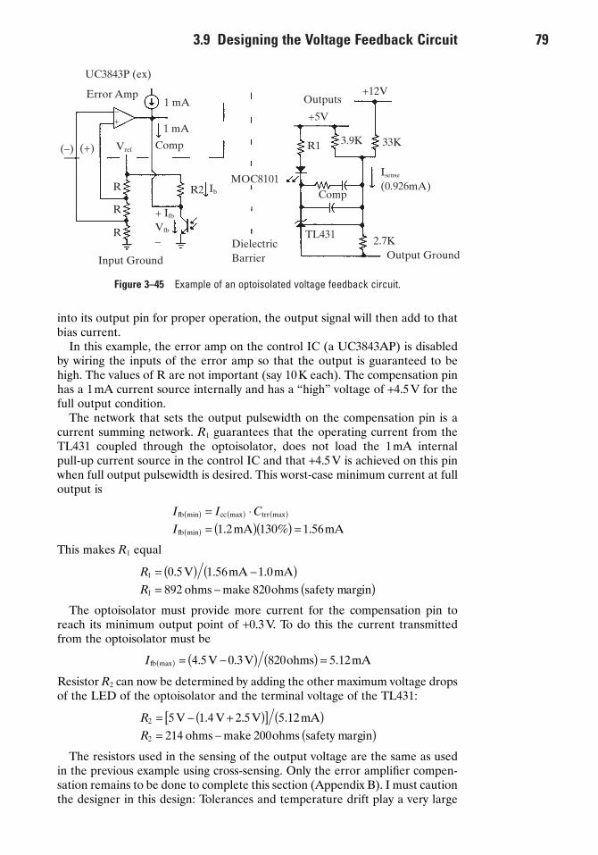
into its output pin for proper operation, the output signal will then add to thatbias current.
In this example, the error amp on the control IC (a UC3843AP) is disabledby wiring the inputs of the error amp so that the output is guaranteed to behigh. The values of R are not important (say 10K each). The compensation pinhas a 1mA current source internally and has a “high” voltage of +4.5V for thefull output condition.
The network that sets the output pulsewidth on the compensation pin is acurrent summing network. R1 guarantees that the operating current from theTL431 coupled through the optoisolator, does not load the 1mA internal pull-up current source in the control IC and that +4.5V is achieved on this pinwhen full output pulsewidth is desired. This worst-case minimum current at fulloutput is
This makes R1 equal
The optoisolator must provide more current for the compensation pin toreach its minimum output point of +0.3V. To do this the current transmittedfrom the optoisolator must be
Resistor R2 can now be determined by adding the other maximum voltage dropsof the LED of the optoisolator and the terminal voltage of the TL431:
The resistors used in the sensing of the output voltage are the same as usedin the previous example using cross-sensing. Only the error amplifier compen-sation remains to be done to complete this section (Appendix B). I must cautionthe designer in this design: Tolerances and temperature drift play a very large
R
R2
2
5 1 4 2 5 5 12214 200
= - +( )[ ] ( )= - ( )
V V V mAohms make ohms safety margin
. . .
Ifb max V V ohms mA( ) = -( ) ( ) =4 5 0 3 820 5 12. . .
R
R1
1
0 5 1 56 1 0892 820
= ( ) -( )= - ( )
. . .V mA mAohms make ohms safety margin
I I C
Ifb min cc max trr max
fb min mA mA( ) ( ) ( )
( )
= ◊= ( )( ) =1 2 130 1 56. % .
3.9 Designing the Voltage Feedback Circuit 79
UC3843P (ex)
Error Amp1 mA
1 mA
CompVref(–) (+)
R
R
R
R2 Ib
+ Ifb
Vfb
–
Input Ground
MOC8101
DielectricBarrier
Outputs
+5V
R1 3.9K
Comp
TL431
+12V
33K
Isense
(0.926mA)
2.7KOutput Ground
–+
Figure 3–45 Example of an optoisolated voltage feedback circuit.

part in the isolated feedback design and they must be accommodated in the partvalue calculations. Optoisolators, for instance the Ctrr, can vary over a range of300 percent, which may necessitate a potentiometer to be added to the circuit.Some optoisolators are sorted by their manufacturers to a narrower Ctrr range,but it is rare and not liked by them. The voltage reference should also be a temperature-compensated variety, such as provided in the TL431.
The issue of output accuracy from unit to unit usually requires that the ref-erence used be trimmed to two percent variation or less, and the resistors withinthe resistor voltage divider be one percent. The accuracy of the outputs thenare these tolerances added together plus any inaccuracies within the trans-former turns.
There can be many variations on the voltage feedback design and only themost straightforward approaches have been shown as these are the mostcommon types of approaches.
3.10 Start-up and IC Bias Circuit Designs
The start-up and bias supply circuit provides the operating voltage for thecontrol IC and power switch drive sections. This circuit is sometimes called thebootstrap start-up circuit. Since all of the power drawn and delivered by thiscircuit is considered a loss, it is important to keep its overall function as effi-cient as possible.
The bootstrap start-up circuit gains in importance for higher input voltages.For input voltages greater than 20VDC where the controller IC and the powerswitch cannot directly use the input voltage for their own power, a start-up/biascircuit must be used. Its function is basically that of a shunt or series linear regulator in order to provide a relatively stable voltage for the controller andpower switch drive circuits.
For starting a power supply from a totally unpowered state, such as experi-enced when input power is first applied to the power supply, current must bedrawn from the input power line. The voltage rating of the start-up circuit mustbe greater than the highest anticipated input voltage including any voltagesurges that might get passed the input EMI filter section of the power supply.For this circuit, a little thought must be given to its desired functionality. Thereare several common functions that the start-up circuit can perform and its func-tion should be appropriate for the operational requirements of the overallsystem.
1. Full functionality of the control/power switch circuit during a short-circuiton the power supply’s output with immediate return to operation upon theremoval of the short.
2. The power supply enters a hiccup restarting mode of operation duringshort-circuits and restarts upon the removal of the short-circuit.
3. Enter a complete shut-down state thus turning off the system during ashort-circuit. The input power must be turned off and then back on inorder to restart the power supply.
The first two modes of operation are the common approaches to the start-upcircuit’s functionality and it is recommended where the system has removablesections such as telephone systems or card-cage systems, or where routineservice is expected and service people may inadvertently create a short-circuit
80 Pulsewidth Modulated Switching Power Supplies

within the load. The shut-down method of functionality is appropriate forimportant instruments where erroneous operation can be detrimental to theinstrument or its operator.
In products where a little added loss is not important, a simple Zener shuntregulator is typically the approach as seen in Figure 3–46. Here the start-upcurrent is constantly being drawn from the input power line, even during steady-state operation. If the start-up current is less than the current required tooperate the IC and driver (~0.5mA), then the power supply has a hiccup mode of recovery. If the start-up current is enough to power the circuit (~10 to15mA), then the power supply remains in a overcurrent foldback state duringshort-circuits and immediately recovers upon removal of the short-circuit. Thedifference is the amount of power lost within the start-up circuit during opera-tion. The amount of hysteresis voltage in any LVI (low voltage inhibit) circuitwithin the control IC affects the hiccup restart of the supply. An IC supplybypass capacitor of 10 mF or more is needed to store enough energy to get thesupply started before its voltage drops and resets the LVI. In general, the largerthe hysteresis voltage, the more certain the supply will start on the first attempt.
For off-line switchers, where continuous current drawn from the input linewould represent a significant loss, cutting off the start-up current during steady-state operation is recommended. After the entire power supply has stabilizedin steady-state operation, the IC and drive circuits can draw all of their powerfrom the auxiliary winding on the transformer. Here the conversion efficiencyis about 75 percent as compared to the 5 to 10 percent. This method is shownin Figure 3–47 is such a circuit. The circuit is a high-voltage current-limited,linear regulator, and cutting off its start-up current is accomplished by reverse-biasing the diode on the emitter and the base-emitter junction during steady-state operation. The small signal transistor must have a VCEO(SUS) greater thatthe maximum input voltage. The collector resistor sustains nearly all the loss.Only a small bias current continues to flow into the base of the transistor andZener diode.
Once again, the designer can choose whether to make the supply operate inthe hiccup mode restarting or to have the control and driver section continueto operate during a short-circuit condition. Choosing the value of the collectorresistor for 0.5 or 15mA current selects the respective operation.
A variation on this method is called the shut-down on overcurrent circuitshown in Figure 3–48. Here the start-up circuit is a discrete, high-voltage, one-shot circuit that is active only during the start-up sequence, but turns completelyoff thereafter. If an overcurrent foldback condition is experienced, the IC anddrive circuits no longer have a voltage supply from which to draw current. This
3.10 Start-up and IC Bias Circuit Designs 81
Vin(DC)
R Vcc
IDz Dz C>10 uF
T
Vaux
Input Return
R: R ≤Vin(min) - VDz
Istart + IDz(min)
PD ≥ Vin(max).(Istart+ IDz(min))
Dz: >500 mW, > Vcc(min) of IC
Figure 3–46 The Zener diode controller supply regulator.

turns off the entire power supply until the input voltage is turned off and thenturned back on.
The designs previously described have worked particularly well for me, butthere are many varying implementations along the same principles of operation.If a different design approach is being contemplated, keep one thing in mind—the start-up period of the switching power supply is the most traumatic periodin its operational life. That is, more failures occur during the start-up periodthan any other period of operation. The sequencing of the various bias suppliesis very critical to the supply. The power switch drivers should always be fullypowered before the control IC begins the switching process. If it is not, thepower switches will not operate in a saturated manner and may therefore faildue to overdissipation.
Another factor is the rated breakdown voltage of resistors. For a one-quarterwatt resistor, the rated breakdown voltage is 250VDC. The one-half watt resis-tor is 350 VDC. To design safely, two resistors in series should be used on allbranches that are connected to the input line in off-line converters.
3.11 Output Protection Schemes
Protection schemes for the outputs of a power supply should be developed care-fully to complement the use and functionality of the end product. Although
82 Pulsewidth Modulated Switching Power Supplies
Vin (DC)
R1
Dz
R2
Q1D1
C
Vcc
D2 T
Vaux
Input Return
R1: R1 =Vin(min)-VDz
IDz(min)
R2: R2 ªVin(min)-VDz
Istart
D1: IN4148 D2: MUR1XO
DZ: 500mW, >Vcc(min) or IC
Q1: VCEO > Vin(max), Ic ª 300 mA
Vin(DC)
R1R2
C1MR816
Q1
R3
T
Dz110uF
Dz2
D3
Vaux
Input Return
R1 ª 220 ohms
R2 ªVin(min) - VD1
Istart
Ton ª 1R3.C1
D1: 1N5253AD2: 1.3Vcc(min), 500 mWQ1: Pwr MOSFET, VDS>Vin(max)
Vcc
Figure 3–47 The high-voltage linear regulator bootstrap start-up circuit (used only at start-up and foldback periods).
Figure 3–48 The overcurrent shut-down circuit.

these circuits are used only in the event of an unusual system failure, one doesnot want additional damage or additional user aggravation to be derived fromthe activation of a protection function. One should also consider the nature ofthe loads, their likely failure modes and causes, and the limits beyond whichfurther damage is caused.
Protection of the load and of the power supply from failures in the load shouldbe an important consideration within all switching power supply designs. It isimportant to know what failures are likely to occur within the switching powersupply and the load. An exercise that is frequently required in military designsis what is called a FMEA (failure modes and effects analysis), where each com-ponent is hypothetically assumed to fail open-circuited and then short-circuited.With such failures, how does each failure affect the other sections of the circuit?This anticipation of failures can make a power supply design robust. It is theresponsibility of the power supply designer to provide protection to the load circuitry from anomalies encountered from the input line and failures withinthe supply and the load circuitry. Often, protection schemes can be cascaded toprovide redundant protection in the event of a failure in a protection circuit. Afuse or a circuit-breaker usually provides such a back-up function.
When considering the method(s) of protection used within a power supplyand any power busing system, it is important to consider the end user of theproduct and the product’s function. The repair philosophy of the product shouldbe carefully reviewed. If the product will have service people routinely “withtheir fingers in the circuits,” then a circuit-breaker, a self-restarting bootstrapstart-up circuit, and a simple overcurrent foldback circuit is the desired combi-nation of circuits. If the product’s function is noncritical and its operation canbe easily done without, then a fuse, an overcurrent shut-down type of start-upcircuit, and overcurrent foldback and/or crowbar circuit may be desired. Someprotection methods may necessitate the equipment being brought into a repairshop for checking prior to being reused. The types of protection philosophiesfall into three categories:
1. Repair after failure (fuses, fusistors, etc.).2. Recovery after failure (circuit-breakers, overcurrent foldback, overvoltage
override circuits, etc.).3. Shut-down after failure, but recoverable when the fault is removed (over-
current shut-down type of start-up circuits, etc.).
Choosing the most appropriate combination of protection schemes can makea large difference in the customer’s perceptions of the product and hence in itsreputation and sales.
There are basically three types of overcurrent protection. These are shown inFigure 3–49. Current-mode control or any primary-side peak current controlleroffers a constant output power limiting when a short-circuit is “soft,” but doeseventually foldback both the voltage and current into hard shorts. When anovercurrent failure presents a lower and lower resistance to the supply, theoutput voltage decreases, but the output current can continue to increase. Thismay produce burning of printed circuit board traces and components. Thisreducing of the output voltage can be useful in conjunction with a shut-downon failure type of start-up circuit. Constant current limiting (see Figure 3–50)is produced when the voltage across a current sensing resistor is amplified andcompared to a reference voltage. When the trip point is exceeded, the outputcurrent is held constant for any greater load. Output current must be sensed forthis type of overcurrent protection. Overcurrent foldback limiting only occurswhen a small amount of the output voltage is used as a threshold reference for
3.11 Output Protection Schemes 83

the trip point of the overcurrent knee. When the current through the currentsense resistor is large enough to exceed the trip point, the voltage is folded backthus also folding back the output current in proportion to the output voltage.This protects the load circuitry from burning (see Figure 3–51).
Overvoltage protection on the output lines can take two forms, the brute force approaches, and the overvoltage override approaches. The brute forceapproaches are the overvoltage clamps and crowbars, as seen in Figure 3–52.These approaches assume that the power supply has failed and cannot limit thecurrent into the load. The most problematic topology is the buck topology,where a shorted series pass unit directly connect the input to the output. Thebuck converter must definitely have a crowbar circuit (if Iout is greater than 1A)or an overvoltage Zener clamp (if Iout is less than 1 A) on its output. For all theother topologies, especially the transformer-isolated topologies, this is not apossibility and therefore a crowbar is a nuisance. Overvoltage Zener diodes onthe outputs can serve as useful insurance in the case of a voltage feedback loopfailure or poor output cross-regulation. An input fuse or circuit breaker isrequired with these forms of overvoltage protection.
The overvoltage override methods assume that the power supply is still operating and the voltage feedback has become open-circuited, or that one of the outputs has become light loaded and its voltage rises above the maximumspecification. These methods have a separate comparator or transistor and resistor dividers wired to each output. The comparator or transistor would thenoverride the error amplifier. These are shown in Figure 3–53.
Choosing the form(s) of protection is always is a matter of economics andboard space. Be creative with your approaches to protection, but check themout carefully under all operating conditions.
3.12 Designing the Input Rectifier/Filter Section
The input rectifier/filter circuit plays a largely unappreciated role within theswitching power supply. The typical input rectifier/filter circuit is composed ofthree to five major subsections: an EMI filter, possibly a start-up surge current
84 Pulsewidth Modulated Switching Power Supplies
OutputVoltage
CurrentFoldback
ConstantCurrent
Vol
tage
CurrentRatedCurrent
ConstantPower
Figure 3–49 Types of overcurrent protection.

limiter, a surge voltage suppressor, a rectification stage (for off-line applica-tions), and the input filter capacitor. Many new ac off-line power supplies arerequired to have power factor correction (PFC). For these applications, designthe input stage described here, then refer to Appendix C. The designs of thetypical input rectifier/filter circuits are shown in Figure 3–54 for both the dc andac applications.
For off-line switching supplies, the first task is to select the input rectifiers.These are standard recovery diodes, such as the 1N400X rectifiers. The majorparameters under consideration are average forward current (IO), surge current(IFSM), the dc blocking voltage (VR), and the anticipated power dissipation (PD).The surge current occurs at power-up and can be greater than 10 times theaverage RMS input current. It is caused by the fully discharged input filtercapacitor taking the classic impulse of current when a step change in voltage
3.12 Designing the Input Rectifier/Filter Section 85
LoD
Co
RCS
LoDfromTransformer Co RCS
V(out)
+
–
Q
ToCompensationPin
RCS =0.7V
I out(max)
Q is a small signal NPN(ex: 2N3904 or similar)
(a)
+
V(out)
–
R1
R2
R3
1K
1nF
100K
1K
ToCompen-sationPin Vref
RCS =Vth
Iout(max)
Vth =Vref (R3)
R2
R1 = R2 ª 1kW
(b)
compR1
R2Rs
MBR130
–+
–+
–+
ToCompen-sationPin Vth
input GND
CTT
CoV(out)
+
–
+
CT: 1:N turns ratioRs ª 20W
R1 & R2: adjust to set foldback current value.
(c)
Figure 3–50 Methods of constant current limiting: (a) discrete overcurrent limiting(constant-current limiting); (b) precision resistive current-sensing overcurrent protection(constant-current limiting); (c) use of a current transformer to sense ac current.
86 Pulsewidth Modulated Switching Power Supplies
D Lo
+
fromtransformer Co Vth
R5
R6V(out)
ToCompensationPin R4
comp
R1R3
RCS
R2
R1 & R2 ª 1KW
R4Gain =
R3(Sets Slope)
R1 = R4
Vth ª 0.3V
RCS =Vth
I(max)
–
+–
Figure 3–51 Overcurrent foldback.
Vout
ZenerDiode
GND
Vz ª 1.2 Vout(rated)
PD > 1W
Tolerance £ 5%
(a)
Vout
SCR
Dz
Q
R1
R2
100WGND
Vg
R1 ª 270W
VDZ ª Vtrip – VBE – VG(TH)
R2 ªIG(min)
Vtrip – 2V
(c)
R1
Isense
R2
8
Vcc
Vth MC3425O/P
DLY
31
7 2 100WCDelay
Vout
SCR
GND
Vtrip = 2.5V(1 +R2R1 )
Isense ª 1mA
R2 =2.5V
Isense
R1 =Vtrip - 2.5V
Isense
CDLY =TDLY
12,500
(b)
GND
Figure 3–52 Overvoltage protection schemes: (a) Zener diode clamp; (b) overvoltagecrowbar; (c) precision overvoltage crowbar.

occurs on its terminals. A thermistor is usually added just following the EMIfilter to protect the ac rectifiers. The “cold” value of the thermistor is typicallybetween 6 and 12 ohms. After start-up, the thermistor heats up and shouldassume a “hot” resistance value of approximately 0.5 to 1.0ohm.
The average current through the input rectifiers is a thermal consideration.Referring to Figure C–1 in Appendix C, you can see the actual waveform flowingthrough the nonpower factor-corrected ac rectifiers. The peak current can beas much as five times the average dc current flowing through the diode. Thiscauses greater heating of the rectifier. To compensate for this, a higher currentdiode is selected to minimize the peak current forward voltage drop and to ridthe die of the heat. In summary, the minimum diode ratings should be
(3.51)
(3.52)
IFSM ≥ 5 · IF (3.53)
The typical diodes for this application areIf the current is <1A: 1N400X
<1.5A: 1N539X<3A: 1N540X<6A: MR75X
I IF in DC≥ ◊ ( )( )1 5. max
V VR in p p≥ ◊ -( )( )1 414. max
3.12 Designing the Input Rectifier/Filter Section 87
Vout
R1
Isense
Vcc
1N4148ToCompensationPin 1M
VrefR4
R2
GND
Op amp: MC33172
Vtrip + Vref(1 + R1R2
)
Isense + 1 mA
R2 +Vref
Isense
R1 +Vtrip - Vref
Isense
R4 ªR1(R2)
R1 + R2
(a)
Vout2
Vout1
R2 R3
DZ1 DZ2ToCompensationPin 2N3904
R1 470 pFGND
(b)
DZ: Vz ª 1.1 Voutx(rated) – 0.7V
Tolerance £ 5%
R1 ª 270W
R2 = R3 ª 100W
–+
Figure 3–53 Methods of overriding the voltage feedback loop in the event of its failure: (a)overvoltage override circuit (when voltage loop goes open-circuited); (b) multiple-outputovervoltage override circuit.

The next operation is to calculate the value of the input filter capacitor. Thedesigner needs to decide how much ripple voltage the supply can tolerate onthe dc input line. The less ripple voltage desired, the larger the capacitor, andthe larger the surge current during the power-up period. There are three majorconsiderations when selecting a capacitor for this function: the value to yieldthe desired ripple voltage, the voltage rating, and the ripple current rating ofthe capacitor.
The typical design goals for the ripple voltage are about five to eight percentof the peak rectified input ac voltage for ac off-line converters and about 0.1 to0.5 volts peak-to-peak in dc-dc converters. The value of the bulk input capaci-tor can be found by
(3.54)
where: fin is the minimum rated ac line frequency for off-line supplies.Vin is the minimum peak rectified value of the ac line.
Vripple is the peak-to-peak droop in voltage desired across the inputcapacitor.
CP
f V Vin
in av
in in min ripple p p
-( )( )
( )
( ) -( )
0 32
.
88 Pulsewidth Modulated Switching Power Supplies
Figure 3–54 Typical ac and dc input filter circuits: (a) ac input filter circuit for a single oruniversal input power supply (common-mode EMI filter shown); (b) a voltage doubling acinput circuit for 110 V and 220 V ac inputs; (c) single dc bus input filter.

The voltage rating of the capacitor should be
(off-line) (3.55)
(dc-to-dc) (3.56)
In ac off-line converters, aluminum electrolytic capacitors are used as theinput filter capacitor. They have proven to be more rugged than any other typeof capacitor in the hazardous environment existing on the ac line. Choosing thefinal capacitor depends mostly upon the expected operating temperature range,quality level, and case dimensions.
The input capacitors in dc-dc converters are much more critical. DC-DC con-verters typically draw much higher ripple currents at the switching frequency ofthe supply. These currents cause internal heating of the input filter capacitorsand shorten their operating life, if they are not selected properly. The inputfilter capacitor needs to have a low ESR and a high ripple current rating. Theentire current waveform seen on the power switch within the power supply isflowing into and out of the input filter capacitor. The input line, because of theexistence of series impedances in the wiring, cannot provide the high frequencycurrent pulses demanded by the power switch inside the switching power supply.The input capacitor serves a very important role of receiving charge at a lowfrequency from the input line and supplying charge to the power switch at highfrequency. Therefore, the current experienced by the power switch is completelyseen by the input filter capacitor.
The designer must convert the current waveform observed at the powerswitch into a worst-case RMS value. Converting a triangular or trapezoidalcurrent waveform into an RMS value depends upon the waveforms peak ampli-tude and its duty-cycle. One can estimate the RMS value of a waveform bybreaking a waveform into simpler waveforms whose RMS value is known. Forexample, a trapezoidal waveform can be broken into a rectangular wave whoseRMS highest value is 50 percent of the peak value (50 percent duty cycle) anda triangular waveform whose highest value is about 33 percent of the peak value.These individual estimated values are then added to estimate the worst casetotal RMS value.
It is unusual to be able to find one capacitor to handle the entire ripplecurrent of the supply. Typically one should consider paralleling two or morecapacitors (n) of 1/n the capacitance of the calculated capacitance. This will cutthe ripple current into each capacitor by the number of paralleled capacitors.Each capacitor can then operate below its maximum ripple current rating. It iscritical that the printed circuit board be laid out with symmetrical traced to eachcapacitor so that they truly share the current. A ceramic capacitor (~0.1mF)should also be placed in parallel with the input capacitor(s) to accommodatethe high frequency components of the ripple current.
Ahead of this section is the EMI filter. The design of the single-line dc filterinductor is found in Section 3.5.7. This inductor has a relatively high value ofdc current flowing through it and wants to isolate the high frequency switchingnoise from the input power bus.
In ac off-line applications the common-mode choke is typically used and itsdesign procedure can be found in Appendix E. The filters resemble “pi” filters,but are actually bi-directional L-C filters. The important function is to filter thenoise generated by the switcher before it exits via the input power lines.
The capacitors used for this function are high-voltage film or ceramic capac-itors that exhibit very good high frequency characteristics. These capacitors
V VW in max> ( )1 5.
V VW in RMS> ( )1 8.
3.12 Designing the Input Rectifier/Filter Section 89

range in value from 0.005 to 0.1mF. Care must be taken as to the working voltagerating of the capacitors. Off-line converters must pass regulatory testing whichplaces an extra voltage stress upon them. The test is called the dielectric with-standing voltage test or “HIPOT.” Any capacitor placed between the input linesto the earth ground lead (green wire) must be able to withstand this test voltage.These voltages are: UL, 1700VRMS (2500 VDC); for VDE, IEC, and CSA, 2500VRMS (3750 VDC). To pass the regulatory agencies in the European common-wealth, special capacitors intended just for this application must be used. Thesecapacitor families are tested and certified for these ac EMI filter applications.
The surge suppression section should be physically placed behind the EMIfilter inductor and before the ac rectifiers (off-line) and before the input filtercapacitor (dc-inputs). All surge suppressors need the series impedance of theEMI inductor to keep them from exceeding their instantaneous energy ratings.The EMI inductor drastically reduces the peak transient voltage and spreads itout over time, thus reducing the instantaneous effects of the transient upon thetransient suppressor. This improves the survivability of the suppressor. Be awarethat different technologies of surge suppressors have different series inherentresistance characteristics. The metal-oxide varistor (MOV) has a relatively highresistance when it is conducting. Semiconductor transorbs exhibit a lower resis-tance. The series resistance affects how much additional voltage will appearacross its terminals during the surge period. For example, a 180 V MOV mayrise to 230 volts at the peak of the transient. This should be considered whenselecting both the input capacitor and the surge suppressor. MOVs, althoughinexpensive, do degrade after suppressing a few high-energy transients andexhibit a higher leakage current. The “trip” voltage of the surge suppressorshould be higher than the maximum high input operating voltage specificationof the supply so that it does not conduct during normal operation. For example,for the 110VRMS line, a 180 to 200V trip voltage is typically used.
A comment on RFI and this circuit: The EMI filter stage should be placedas close to the entrance of the power feed wire into the enclosure as possible.The conducted EMI from outside can be reradiated into the case if the wirelength is too large before the filter. Conversely any RFI may be picked up bythe long length of power cord inside the case and radiated outside where theregulatory testers will feel they’ve earned their pay by “nabbing” another errantproduct. Refer to Appendix E for noise control methods.
3.13 Additional Functions Normally Associated withPower Supplies
Additional functions are added to the basic switching power supply so that thesupply’s operation better complements the function of the overall product. Theoverviewed functions are those routinely found in some switching power sup-plies, but certainly are not all of the possible functions. These functions mayinclude: synchronization, undervoltage alerts, input undervoltage inhibit, andpartial supply shut-down.
3.13.1 Synchronization of the Power Supply to an External SourceSynchronization allows the switching power supply to be phase-locked withanother circuit in the external product. This may be necessary for circuits which
90 Pulsewidth Modulated Switching Power Supplies
include CRTs (cathode ray tubes), analog-to-digital and digital-to-analog con-verters, etc. The noise generated by the switching power supply could interferewith these circuits. For example, lines may be displayed on a CRT at the instantwhen the power switch and retifiers turn on or off. Noise spikes picked up inthe sensitive input signals of a comparator can cause it to compare at the wronginstant within an A-to-D converter. To solve this, it may be desirable to lock theclock within the supply to the timing of these sensitive circuits to try to placeany noise spikes in a harmless point in time.
Some power supply control ICs have synchronization inputs for this purpose.For those ICs which have an oscillator, but not a synchronization pin, the circuitin Figure 3–55 can be used. The frequency on the IC must be set lower than thesynchronization signal. The sync signal causes the oscillator to prematurelytime-out.
3.13.2 Input, Low Voltage InhibitMany times it is desirable to shut the product off during brownout conditions.These are conditions where the input voltage falls below the minimum specifi-cation for normal operation. This condition can cause a voltage-mode con-trolled power supply to enter a type of “latch-up” mode where the supply wouldquickly jump to its maximum duty cycle and would no longer control the outputregulation. This could be destructive to the supply and the loads when the inputvoltage returns to normal levels. Also, at the lower input voltages, the higherpeak currents flowing through the power switches can cause them to fail due tooverdissipation. To avoid this, a simple voltage comparator sensing the inputline is needed as in Figure 3–56.
3.13 Additional Functions with Power Supplies Associated 91
39K 0.001uF
Ct
FromSquarewaveSource
Control IC
Oscillator f(osc) ª 0.9 F(sync)
+Vin
R1
+Vin(DC)
R2
1MW (hysteresis)
R3
+–
Isense
Vref
DC input GND
ToCompensationPin
R2 = Vref
Isense
R1 =Vin(min) - Vref
Isense
R3 =(R1)(R2)R1 + R2
Op Amp: single supply, rail-to-rail type
Figure 3–55 Synchronizing a switching power supply (no sync pin on the IC).
Figure 3–56 Input undervoltage shutdown circuit.

3.13.3 Impending Loss of Power SignalFor products that include microprocessors, floppy or hard disk drives, or anyother device where a sudden loss of power during its operation could causedamage to the product or injury to the user, it is recommended that a powerfail signal be issued by the power supply. For a simple microprocessor system,a simple low voltage sensor on the +5 volt line may be sufficient. If the productincludes any electromechanical devices which may require a finite time to insti-tute an orderly shut down, a longer period of time may be required. This meanssensing the power supply’s input voltage and making the input filter capacitorlarger so that the supply can maintain a regulated output longer. Caution mustbe practiced since large input filter capacitors will significantly increase the turn-on surge current through any input rectifiers, which can cause rectifier failures.This method may yield as much as 8 to 15mS of additional time to shut thedevice down. These circuits can be seen in Figure 3–57.
92 Pulsewidth Modulated Switching Power Supplies
Figure 3–57 Power fail indicator/alert circuits: (a) a 5 V under-voltage indicator; (b) anunder-voltage indicator for any voltage; (c) power-down signal derived from the input line(longest warming period).

3.13.4 Output Voltage Shut-downSometimes it is desirable to turn off a section of the product but leave otherportions operating. This is typically the case in laptop computers for powersavings or consumer appliance applications, such as CRT monitors, televisions,and stereo equipment.
Many consumer appliances must place themselves in the standby mode whenthe user has walked away from the product. This type of operation is called“green certified.” This certification dictates that the product must use less than5 watts of power while in the standby mode. The switching power supply alonewould have quiescent operating current greater than 5 watts, so a very low powerswitching power supply, with much lower quiescent currents, can be used topower only that portion of the product needed to reactivate the product upondemand.
In the case of power factor corrected ac power supplies, the main convertercan be turned off and the circuit to remain active could use the auxiliary voltageon the power factor transformer. The power factor circuit would run at a muchreduced pulsewidth and/or frequency.
The portable equipment market usually needs to turn off any temporarilyunused circuits to extend its battery life. In this case, a simple series MOSFETswitch can be used. The RDS(ON) should be as low as possible to minimize thepower dissipation within the MOSFET switch. These approaches are shown inFigure 3–58.
3.14 Laying Out the Printed Circuit Board
The final stage in the design of any switching power supply is the physical designof the printed circuit board (PCB). If it is designed improperly, the PCB couldcontribute to the supply’s instability, and radiate excessive electromagneticinterference (EMI). The role of the designer is to insure a good PCB design byunderstanding the physical operation of the circuit.
Switching power supplies contain signals that are rich in high frequencies andany PCB trace can act as an antenna. A trace’s length and width affect its resis-tance and inductance, which in turn affects its frequency response. Even tracescontaining dc signals can pick-up RF signals from neighboring traces and causecircuit problems or even reradiate the interfering signal again. All traces thatcarry ac current must be made as short and wide as possible. That means thatany power-handling components that connect to a trace and to other powertraces must be located adjacent to one another. The length of a trace is directlyproportional to the amount of inductance and resistance the trace will exhibit.Its width is inversely proportional to the trace’s inductance and resistance. Thelength dictates the wavelengths to which the trace will respond. The longer itslength, the lower the frequency the trace can receive and transmit and the moreRF energy it is susceptible to.
3.14.1 The Major Current LoopsThere are four current loops inside of every switching power supply. Each ofthese loops must be kept separate from one another. They are listed in orderof their importance to a good PCB layout.
3.14 Laying Out the Printed Circuit Board 93

1. The power switch ac current loop.2. The output rectifier ac current loop.3. The input source current loop.4. The output load current loop.
These loops can be seen in Figures 3–59 a, b, and c for the three major switch-ing power supply topology types.
The input source and output load current loops typically do not present prob-lems. The current within these loops is largely composed of dc flow with somesmall ac current summed onto the waveform. These two loops typically also havespecial filters to discourage the escape of ac noise into the surrounding envi-ronment. The terminals of the input and output filter capacitors should be theonly places where the input and output current loops, respectively, connect tothe power supply. The input loop charges the input capacitor with a near-dccurrent but is unable to supply the high frequency current pulses required bythe switching power supply. The filter capacitor’s main role is to perform thiswide band, energy reservoir function. The output filter capacitor similarly storesthe high frequency energy from the output rectifier and allows the output loadloop to remove the energy in a dc fashion. Therefore, the terminals of the input
94 Pulsewidth Modulated Switching Power Supplies
Vin
MC34065P
ENABLEControlSignal
Ct
Vout1
+
–
+
Vout2 (Switched)
–
(a)
VoutMTP23P06 Switched
+Output10K10V
4.7K
ControlSignal
3.3K
1K
MPS3904
GND(b)
Figure 3–58 Methods of switching power buses: (a) dual switching power supply withenable; (b) a dc power switch.

and output filter capacitors are very important. If the connections between theinput or output loops and the power switch or rectifier loops are not routeddirectly to the capacitor’s terminals, then ac energy will go around the input oroutput filter capacitors and escape into the environment via the input andoutput current loops.
The power switch and rectifier ac-current loops contain very high trapezoidalcurrent waveforms typical in PWM switching power supplies. These waveformsare rich in harmonics which extend far above the basic switching frequency.These ac currents can have peak amplitudes two to five times that of the
3.14 Laying Out the Printed Circuit Board 95
+
-
Vin
Cin
Input LoopPower Switch Loop Rectifier Loop
Output Loop
Rload
Cout
SW
L
(b)
Input Loop
+
-
Vin
Cin
Power Switch Loop Rectifier Loop
Cout
SWL
Rload
Output Loop
(a)
+
-
Vin
Input Loop Power Switch Loop
SW
Rectifier Loop Output Loop
Rload
Cout
T
Cin
(c)
Figure 3–59 The major current loops within the major switching power supply topologytypes: (a) the nonisolated buck converter; (b) the nonisolated boost converter; (c) thetransformer-isolated converter.

continuous input or output dc currents. The transition times are typically about50nS. These two loops, therefore, have the greatest ability to create electro-magnetic interference (EMI).
These ac current loops should be routed before any other traces in the powersupply. The three major components that make up each loop: the filter capacitor, the power switch or rectifier, and the inductor or transformer mustbe located adjacent to one another. The components must also be oriented suchthat the current path between them is as short as possible. A good example ofa layout of the power section of a buck (or step-down) converter can be seenin Figure 3–60.
The traces within these loops also have the greatest affect on the converter’smeasured efficiency. If a significant voltage drop is experienced on any of thesetraces, the converter will appear less efficient, because it is operating at a lowervoltage (hence higher current). But, if DVMs or meters are used to calculateits efficiency, the input voltage readings will be higher than the converter is actually experiencing, thus creating a misleadingly larger VxI product.
3.14.2 The Grounds Inside the Switching Power SupplyThe grounds represent the bottom branch of the current loops discussed earlier.Grounds, though, serve a very important function as the common point of ref-erence for the circuitry. Therefore, grounds must be carefully placed in thelayout. Intermingling these grounds will cause problems with the stability of thepower supply.
There is an additional ground to consider and that is the control ground. Thisis the ground connected to the control integrated circuit and all of its associ-ated passive components. This ground is extremely sensitive and should beplaced after the other ac current loops are placed. There are very specific pointswhere the control ground connects to the other grounds. The connection, ingeneral, is at the common-end of any component across which the control ICwants to sense a small voltage. These points would include the common end ofthe current sense resistor in a current-mode switching converter, and the bottomend of the output voltage resistor divider. The purpose is to create a low-noiseKelvin connection between the sensing components and the sensitive inputs to
96 Pulsewidth Modulated Switching Power Supplies
Gate
Vin
+
-
Diode ControlGroundConnection
Vout
+
-
InductorPowerSwitch
Cin
Cout
Figure 3–60 A good layout for a buck converter.

Figure 3–61 The ground arrangements for the major converter topologies: (a) thenonisolated dc/dc converter; (b) the nonisolated, transformer-coupled converter; (c) theisolated, transformer-coupled converter.
3.14 Laying Out the Printed Circuit Board 97
Vfb+
-
Vin
Join
Cin
Input SourceGround Power
Switch Ground
Controller
Analog GND
SWL
Vout
Cout
Join
Output Load GroundOutput
Rectifier Ground
Join
(a)
+
-
Vin
InputSourceGround
Power SwitchGround
Join
Cin Controller
Drive
Analog GNDJoin
RCS
SW Output RectifierGround
Join
Cout Vfb
+
-
Vout
T
OutputLoadGround
Analog Control Ground
(b)
+
-
Vin
Join
Cin
fb
Controller
Analog GND
Drive
Power SwitchGround
Join
RCS
SW Output RectifierGround
Cout
Join
T
Vfb
+
-
Vout
Output AnalogGround
(c)
the voltage error or current amplifiers. If the control ground is connected at anyother points, noise generated within those loops will be summed onto controlsignals, therefore adversely affecting the control IC’s proper functioning.
The grounds for the three major switching power supply topology types canbe seen in Figure 3–61.

Each of the high current grounds must be short and have wide traces. As ageneral rule, the common terminal of the filter capacitors should be the onlypoints where the other grounds couple into the high current AC grounds. Theonly exception may be the control ground.
3.14.3 The AC Voltage NodeThere is one node within each switching power supply that has the highest acvoltage compared to the others. This node is the ac node found at the drain (orcollector) of the power switch. In nonisolated dc/dc converters, this node is alsoconnected to the inductor and catch (or output) rectifier. In transformer-isolated topologies, there are as many ac nodes as there are windings on the trans-former. Electrically, they still represent a common node, only reflected throughthe transformer. Special attention must be paid to each ac node separately.
This node(s) presents a different problem. Its AC voltage can be easily capac-itively coupled into any adjacent traces on different metal layers, as well asradiate EMI. Unfortunately, it is generally the trace that must also act as aheatsink for both the power switch and the rectifiers, especially in surface mountpower supplies. Electrically, the trace wants to be as small as possible, but ther-mally, it wants to be large. There is one good compromise in the surface mountdesigns, and that is to make the top PCB island identical to the bottom PCBisland and connect them with numerous vias (or thru-hole connections). Thiscan be seen in Figure 3–62.
This technique greatly reduces the capacitive coupling to other traces whilemore than doubling the heatsink volume and surface area. In thru-hole appli-cations, one must keep the other signals and grounds, away from the highvoltage trace and any of its heatsinks. In off-line converters, the earth groundcan pick-up energy from this node through the heatsink (separated from thedrain tab with an insulator) and allow it to exit the product via the ac plug.
98 Pulsewidth Modulated Switching Power Supplies
Power Device Via
PCB top
PCB bottomPlated-ThruHole
Figure 3–62 A good method for enhancing the heatsinking capabilities of a PCB island andminimizing capacitive coupling to other PCB traces.

3.14.4 Paralleling Filter CapacitorsFrequently, capacitors are placed in parallel to reduce the combined equivalentseries resistance (ESR) of the filter capacitor function. This practice also allowseach capacitor to “share” a portion of the overall ripple current such that eachcapacitor can operate within its ripple current specification. Equal “sharing” ofthe ripple current can only occur when the trace impedance between each ofthe capacitors and the source of the ripple current is identical to one another.This means that the traces between the rectifier or the power switch must be ofequal length and width for each capacitor.
The temptation is to place capacitors in a row and wire them sequentially asseen in Figure 3–63a. This arrangement causes the capacitors closest to thepower switch or rectifier to experience much more ripple current than the othercapacitors further away. This shortens the life of the closer capacitors. Figure3–63b shows a better way to arrange the traces for paralleled capacitors.
The designer should attempt to keep the capacitors “radially symmetric” fromthe ripple current source for both sides of the loop.
3.14.5 The Best Method of Creating a PCB for a Switching Power SupplyThe best method of creating a layout for a switching power supply is analogousto its electrical design. The best design flow is as follows.
3.14 Laying Out the Printed Circuit Board 99
Transformer
Rectifier
+Vout_
Cout
Cout
(b)
Transformer Rectifier
+Vout_
Cout Cout
(a)
Figure 3–63 Laying out paralleled capacitors: (a) a poor layout for paralleled capacitors; (b)a better layout for paralleled capacitors.

1. Place the transformer or inductor.2. Layout the power switch current loop.3. Layout the output rectifier current loop(s).4. Connect the control circuitry to the ac power circuits.5. Layout the input source loop and input filter.6. Layout the output load loop(s) and output filters.
As a good rule, the designer should “fill” the PCB with metal. That is, thereshould not be large areas of bare fiberglass. Grounds and power traces shouldbe widened to fill these blank areas. This is a good practice for two reasons:first, the converter radiates heat better, and secondly, large copper areas captureand dissipate RF energy better by promoting eddy currents to flow.
Of course, the power supply is usually left to the last moment, so its allocatedarea is usually too small and its location is poor. This all means that the flowoutlined above usually cannot be strictly followed, so each designer must do thebest he or she can, by understanding the important electrical factors.
3.15 PWM Design Examples
Today’s switching power supply market has two approaches to the design ofswitching power supplies: the brut-force design from the ground-up style, andthe copy out of the data sheet style. Although there are many good controllerICs being made in the market today, many of which have a “pre-packaged”design procedure conveyed in the data sheet, the purpose of this book is to givea deeper, more fundamental understanding of the topic. Therefore, the follow-ing design examples contain controller ICs that require design expertise to com-plete the power system. These design examples contain basic truths about thedesign of switching power supplies that transcend the “power supplies madeeasy” methods of some of the IC suppliers. The design of the magnetic com-ponents, feedback loop compensation, and input and output filtering still hold true.
The following examples, though tedious, should provide a good insight intothe design process of a PWM switching power supply.
3.15.1 A Board-level 10 Watt Step-down Buck ConverterApplicationThis switching power supply can be used for a board-level regulator where alinear regulator would create too much heat for the board to dissipate. A looselyregulated pre-regulator produces a distribution voltage of between +10 to +18V. The output voltage of the board-level regulator is +3.3V.
This design example purposely avoids the use of a highly integrated buck con-troller IC. It would be instructional to show the selection and design processinvolved in a switching power supply. Refer to Figure 3–65
Design specification
Input voltage range: +10V - +14VDCOutput voltage: +5VDCMaximum output current: 2AOutput ripple voltage: +30mV p-pOutput regulation: +/- 1%
100 Pulsewidth Modulated Switching Power Supplies

“Black box” predesign estimates
Output power: (+5.0V)(2A) = 10.0W (max)Input power: Pout/Est. Effic. = 10.0W/0.80 = 12.5WPower switch loss: (12.5 - 10W)(0.4) = 1.0WCatch diode loss: (12.5 - 10W)(0.6) = 1.5W
Input average currents
Low input: (12.5W)/(10V) = 1.25AHigh input: (12.5W)/(14V) = 0.9AEstimated peak current: 1.4 (Iout(rated))
1.4(2.0A) = 2.8A
The desired frequency of operation is 100kHz.
Inductor design (refer to Section 3.5.5)The worst case operating condition is at the high input voltage.
where: Vin(max) is the maximum possible input voltage.Vout is the output voltage.
Iout(min) is the lightest expected load current.fsw is the operating frequency.
The inductor is to be a surface mount toroid on a J-leaded plastic mountingboard. There are standard surface mount inductors available from many sup-pliers. I have chosen the part DO3340P-104 from Coilcraft.
Selection of the power switch and catch diodePower switch. The power switch is going to be a P-channel power MOSFET. Themaximum input voltage is 18VDC. Therefore, a VDSS rating of +30VDC orhigher will be satisfactory. The peak current is 2.8A. It is also desired to keepthe heat dissipation less than 1 watt so the estimated RDS(on) should be lessthan:
I will select the ubiquitous FDS9435 P-channel MOSFET with an on-resistance of 45 milliohms packaged in an SO8 package.
Catch diode. The catch diode needs to be a schottky diode to minimize the con-duction loss and the switching loss of the function. The diode that has a rea-sonable forward voltage drop at the 3A peak current is the MBRD330 with a0.45V drop at 3A (at +25°C).
The output capacitor (refer to Section 3.6)The value for the output capacitor is determined by the following equation.
R P IDS on-max D est pk est
W A milliohms maximum
( ) ( ) ( )= ( )= ( ) ( ) < ( )
2
21 2 8 127.
LV V V V
I f
L
min
min
.
. ..
in max out out in max
out min sw
V V V V
A kHzH
( ) ( )
( )
-( ) -( )
-( ) -( )( )( )
=
1
1 414 5 1 5 14
1 4 0 5 10082 6m
3.15 PWM Design Examples 101

The major concern of both output and input filter capacitors is the ripplecurrent entering the capacitor. In this application, the ripple current is identi-cal to the inductor ac current. The maximum limits of the inductor current is2.8A for I peak and about one-half the maximum output current or 1.0A. Sothe ripple current is 1.8 A p-p or an estimated RMS value of 0.6 A (about one-third of the p-p value).
I will be using a surface mount tantalum capacitor because they typicallyexhibit about 50 percent of the ESR of electrolytic capacitors. I will also derate the rating of the candidate capacitors by 30 percent at +85°C ambienttemperature.
The best candidate capacitors are from AVX, which have very low ESR andthus can handle very high levels of ripple current. These capacitors are excep-tional and not typical. One piece of these could handle the output demands.
AVX:TPSE477M010R0050 470mF (20%), 10V, 50mohm, 1.625 ArmsTPSE477M010R0100 470mF (20%), 10V, 100mohm, 1.149 ArmsNichicon:F751A477MD 470 mF (20%), 10V, 120mohms, 0.92 Arms
There are very few surface mount capacitors with the desired value, voltagerating, and low ESR all in one part. It would be more conservative to paralleltwo capacitors of no less than one-half the desired capacitance value. This allowsmany more second sourced capacitors to be used and lowers the ESR. Lets usetwo 330mF, 10V tantalum capacitors in parallel. The Candidates now become:
KEMET:T510X337M010AS 330 mF (20%), 10V, 35mohms, 2.0 Arms
Nichicon:F751A337MD 330 mF (20%), 10V, 150mohms, 0.8 Arms
The input filter capacitorThis capacitor experiences the same current waveform at the power switch,which is a trapezoid with an initial current of about 1A rising to 2.8A with verysharp edges. This capacitor has much more rigorous operating conditions thanthe output filter capacitor. I will estimate the RMS value of the trapezoidalcurrent waveform as a piecewise superposition of two waveforms, a rectangu-lar 1A peak waveform and a triangular waveform with a 1.8A peak. This yieldsan estimated RMS value of 1.1A. The value of the capacitor is then calculatedas:
Capacitors at the higher voltages have smaller capacitance values. There willbe two 68 mF capacitors in parallel. The candidates are:
CP
f V
C
inin
sw ripple p p
in
W
kHzF
=( )
=( )( )
=-( )
2 2
12 5
100 1 0125
.
.m
CI DC
f V
C
out minout max
sw ripple p p
outA V V
kHz mVF
( )( ) ( )
-( )
( )
-( )( )
( ) -( )( )( )
=
1
2 1 5 14
100 30429
min
min m
102 Pulsewidth Modulated Switching Power Supplies

AVX: (2 required per system)TPS686M016R0150 68 mF (20%), 16V, 150mohms, 0.894Arms
AVX: (3 required per system)TAJ476M016 47mF (20%), 16V, 900mohms , 0.27ohms (net)Nichicon: (3 required per system)F721C476MR 47mF (20%), 16V, 750mohms, 0.19ohms (net)
Selecting the controller ICThe desired features one might look for in a buck controller IC would be:
1. Ability to operate directly from the input voltage.2. Pulse-to-pulse overcurrent limiting.3. Totem-pole MOSFET drivers.
There are many buck controller ICs on the market, but the one that was chosenis the UC3873. The internal reference presented to the voltage error amplifieris 1.50V+/- 2 percent.
Setting the frequency of operation (C3)From the datasheet, one sets the frequency by the following equation.
Current sense resistor (R1)The type of protection on this IC is a pulse-to-pulse current sense that cuts offthe power switch instantly upon exceeding a 0.47 V threshold. I will allow a 25percent margin between the expected peak current and the protection cutoffthreshold (protection 1.25(2.8A) = 3.5A).
The closest standard value of sub-one ohm resistors is 0.1ohms.
Voltage sensing resistor divider (R3 and R4)R4 (bottom resistor)
This makes the actual sense current 1.006mA.R3 (top resistor):
Compensating the voltage feedback loop (refer to Appendix B)This is a voltage-mode, forward converter. To produce the best transientresponse time, a 2-pole, 2-zero method of compensation is going to be used.
Defining the control-to-output characteristicThe output filter pole is determined by the filter inductor and capacitor and isa -40dB/decade rolloff. Its nominal corner frequency is
fL C
f
fp
o o
fpH F
Hz
=
=( )( )
=
1
211
21 100 660619
p
p m m
R3 5 0 1 5 1 006 3 48= -( ) ( ) =. . . .V V mA K ohms 1%
R4 1 5 1 1 49= ( ) ( ) =. .V mA K ohms 1%
R1 0 47 3 5 0 134= ( ) ( ) =. . .V A ohms
C f
Ct
t
= ( )[ = ( )( )=
1 15 1 15 100666 680
k k kHzpF the closest value is pF
sw
3.15 PWM Design Examples 103

The zero caused by the output filter capacitor(s) is (ESR is two 120mohms inparallel)
The intrinsic absolute gain of the power circuit at dc is
Locating the compensating poles and zeros in the error amplifierThe gain cross-over frequency of the closed loop should not be any higher than20 percent of the switching frequency (or 20kHz). I have found that gain cross-over frequencies of 10kHz to 15 kHz are quite satisfactory for the majority ofapplications. This yields a transient response time around 200uS.
fxo = 15kHz
First one assumes that the final closed loop compensation network will havea continuous -20dB/decade slope. To achieve a 15kHz cross-over frequency,the amplifier must add gain to the input signal and “push-up” the gain curve ofthe Bode plot.
This is the gain needed at the midband plateau (G2) to achieve the desiredcross-over frequency.
The gain exhibited at the first set of compensating zeros is
To compensate for the double filter pole, I will place two zeros at one-half thefilterpole frequency:
fez1 = fez2 = 310Hz
The first compensating pole will be located at the capacitor’s ESR frequency(4,020Hz).
fep1 = 4,020Hz
The second compensating pole is just used to maintain high frequency stabilityby depressing the gain above the cross-over frequency.
fep2 = 1.5 fxo = 22.5kHz
Now one can begin calculating the component values within the error amplifier.
Cf A R
C
7
7
1
2 2 3
1
21 15 5 2 3 48586 560
=( )( )( )
=( )( )( )
=p xo kHz k
pF make pF. . W
G G f f
G
A
1 2
1
1
20 14 3 20 310 402080 4
= + ( ) = + + ( )= -= - ( )
Log dB Log Hz HzdB
absolute equivalent
ez2 ep1 .
.
G f f GDC
G G
A A
xo xo fp
xo
xo
Log Log kHz Hz dBdB
absolute equivalent
= ( ) - = ( ) -= = += = ( )
20 20 15 619 13 42 14 32 5 2
..
.
A V V
G ADC in error
DC DC
V VLog dB
ª = ( ) ( ) == ( ) =
D 14 3 0 4 6620 13 4
. ..
f
R Czesr
esr o m FHz= =
( )( )=
1
2
1
21 60 6604020
p mW
104 Pulsewidth Modulated Switching Power Supplies

Refer to Figure 3–64.
3.15.2 Low-Cost, 28-Watt PWM Flyback ConverterApplicationThis power supply is going to provide power for a piece of process control instru-ment. The instrument receives its power from a +24V bulk power supply whichalso provides transformer isolation from the input bus voltage to the unit. Pleaserefer to Figure 3–66.
Specifications
Vout: +5VDC at 2A maximum current, 0.5A minimum.+12VDC at 0.5A-12VDC at 0.5A+24VDC at 0.25A
Vin: 18 to 36VDC required operational range+24VDC nominal input line voltage
“Black box” pre-design considerations (refer to Section 3.4)
This indicates that a #18AWG wire or equivalent should be used on the primarywinding of the transformer.
Select the frequency of operation of the power supply to be 40kHz (or Ton(max)
= 12.5uS).
Designing the flyback transformer (refer to Section 3.5.5)
L V T I Spri in min on pk V AH
= ◊ = ( )( )=
( ) 18 12 5 8 5526 3
. ..
mm
I P Vpk out in min W V5Amps
ª ◊ = ( )=
( )5 5 5 5 28 188 5
. ..
P
P P
I P V
I P V
out
in out
in high in in low
in op in in nom
V A V A V A V AWatts
effic est WWatts
W VAmps
W V
= ◊( ) + ◊( ) + ◊( ) + ◊( )== ( ) = ( )== = ( )== = ( )=
( ) ( )
( ) ( )
5 2 12 0 5 12 0 5 24 0 2528
28 7537 3
37 3 182 07
37 3 24
. . .
..
..
.11 55. Amps
R A R
Cf R
C
R R A
C
2
6
1
6
5
10
1 1 0 4 3 48 1 39 151
2 2
1
2 310 1 52 9 2 2
2 2 1 5 0 4 3 75 3 91
2
= ( )( ) = ( )( ) =
=( )( )
=( )( )
== = ( ) ( ) =
=
. . .
.. .
. . . .
k k make k
Hz kF or F
k k make k
ez
W W W
W
W W W
p pm m
p ff R
Cfez kHz kpF make pF
2
10
5
1
2 22 5 3 91814 1800
( )( )=
( )( )=
p . . W
3.15 PWM Design Examples 105
Check the energy throughput of the core
I will use an MPP toroid core. The core sizing procedure is contained in Section3.5.5. Estimate the core size required:
E LI L IL pri pk mH A= = ◊ ( ) = ( )( )=
“ ” . ..
22 2
0263 8 551 92
P fL I Hpkout est pri
Watts OK( ) = ◊ ( ) = ( )( )
=
2 22 40 000 26 3 8 55 2
38 45, . .
. —m
106 Pulsewidth Modulated Switching Power Supplies
+ 80
+ 60
+ 40
+ 20
0
- 20
- 40
- 60
0.1 1 10 100 1 k 10 k 100 k 1 MFrequency (Hz)
(a)
Control-to-Output
Closed Loop
Error Amp
fxo
Gai
n (d
B)
Control-to-Output0
- 90
- 180
- 360
- 270
0.1 1 10 100 1 k 10 k 100 k 1 M
Error Amp
Closed Loop
Frequency (Hz)(b)
Pha
se (
Deg
rees
)
Figure 3–64 The gain and phase Bode plots for the design example 3.15.1: (a) the phaseplot for the buck converter; (b) the phase plot for the buck converter.

Reference to Figure 3–21 yields the part number 55310-A2 with a perme-ability of 125. This core has an AL of 90mH/1,000T.
The number of turns for the primary is:
The number of secondary turns on the lowest voltage (+5V) output (assuminga Schottky rectifier) is
The other windings (assuming ultrafast rectifiers) are
The amount of error in each output is
+/-12 V: +0.3 volts+24 V: +0.4 volts acceptable
I chose an autotransformer style secondary which means that the higher voltagewindings will include the lower voltage windings. The turns associated with thisand the wire sizes are
+5V: 5 turns, #17AWG (use 3 strands of #22AWG)+12V: 7 turns, #21AWG
NV V N
V VN
N V
22 1
1
12
24
12 0 0 9 5 5 0 0 5
11 73 12 1224 0 0 9 5 5 0 0 5
22 6 23
=+( )
+( )= +( )( ) +( )= -( )= +( )( ) +( )=
+( )
+( )
D2
D1
V V T V
Turns round to turns V winding has the sameV T V
turns—round to turns
. . . .
.. . . .
.
NN V V
V
N
secpri o D
in min
V T V Vturns round down to turns
=+( ) -( )
◊+( ) = +( )( ) ( )( )
=
( )
1
5 17 5 0 0 5 50 18 505 19 5
∂
∂max
max
. . % %.
Npri mH mHturns round down to 17 turns
= ( )= -
1000 0 0263 9017 09
1 2.
.
NL
Apri
pri
L
= 1 000,
3.15 PWM Design Examples 107
+ Vin
GND
C1 C2 C3
C4 C5
R1 Q1
U1
4
7 8 6 12
53UC3573
R2C6
C7
L1
D1 C8 C9
R3
R4
+ Vout
R5
C10
GND
Figure 3–65 A 10-watt buck (step-down) converter.

-12V: 12 turns, #21AWG+24V: 11 turns, #26AWGpri: 17 turns, #19AWG (use 2 strands of #22AWG)
Transformer winding techniqueIt is not economical to bifilar wind all the windings of the transformer together.Instead a selective bifilar winding technique will be used. The primary windingwill be twisted together with the +24V winding and the +12V and -12V wind-ings will be twisted together prior to winding them on the core. The +24Vwinding will act as the catch winding for the primary and will reduce the voltagespike during the turn-off of the power switch.
The +5V winding is wound first, distributed equally around the circumfer-ence of the toroid. Next the primary/+24V bundle is wound evenly around thecore. Lastly, the +12V and -12V bundle is wound on the core. This windingcan physically “squeeze” between the last winding.
For production considerations, the typical mounting approach is to place thefinished toroid on a terminal board and pot the toroid assembly. This makes theassembly impervious to handling damage and allows the assembly to be easilyplaced into a PCB. Estimated parts cost approximately $2.50 U.S.
Selecting the power switch and rectifiersPower Switch. There is a distinct advantage in using a power MOSFET in thisapplication. It should have less drive and switching losses.
use 100VID: For flyback-mode converters it is a good idea to select a power switch averagecurrent rating of about 1.5 times the maximum average input current of thesupply. Another consideration is the loss. By overspecifying the current theI2RDS(on) loss (conduction loss) can be reduced with very little penalty on costand input capacitance.
Use the MTP10N10M. I have selected the current sensing style of powerMOSFET since I wish to implement a current-mode controller and this willreduce my sensing losses by three orders of magnitude.
Rectifiers.+5 Voutput
Use the 1N5824 (3A).+/-12V output (see above procedure). Use the MUR110 (D5 and D7).+24V output. Use the MUR110 (D4).
The output-filter section (refer to Section 3.6)The values for the output filter capacitors are to be determined by using Equation 3.36.
V V V N N
I I
R min out in max pri
F min out max
V VAmps
( ) ( )
( ) ( )
> - - ( )[ ]> + + ( ) =ª =
sec
.5 36 5 17 15 62
ID min A Amps( ) > ( ) =1 5 2 07 3 11. . .
V V V N N V
L
DS min out D pri sec in max
V V T T VV neglecting any spikes caused by leakage
( ) ( )> +( )( ) +> +( )( ) +> ( )
24 4 0 9 17 23 3654 7
. ..
108 Pulsewidth Modulated Switching Power Supplies

The switch-mode controllerIn attempting to select a controller IC one should make a list of the importantdesired for the design. Also make a “nice but nonessential” list.
Essential “Nice—but”Low parts count Undervoltage lockoutCurrent-mode control Low Isense thresholdMOSFET driver output (totem-pole) 50 percent duty cycle limitingSingle output driverLow cost
After reviewing the list of popular controller ICs, the UC3845P appears tosatisfy all the above requirements. (I also chose it because of its instructionalnature.)
Referring to the data sheet in the Motorola “Linear and Interface IntegratedCircuits” data book, the basic schematic implementation is given in the appli-cation figures. The designer need only determine the values for the timing resis-tor and capacitor, and the current-sense resistor. All of the other componentsare involved with the Vcc supply and the feedback compensation, which will bedesigned later. Looking at the “Timing Resistor vs. Oscillator Frequency” graphand wishing to operate the supply at a nominal 40kHz, one determines a valueof
This value will no doubt need to be adjusted during the breadboard stage.
The voltage feedback section (refer to Section 3.9)In order to enhance the cross-regulation of the multiple outputs, it is desired tosense a portion of all the positive output voltages. To do this, one must investi-gate the technology of the circuits that must draw their power from the outputs.The hypothetical loads, in this case, are
+5V A microcontroller and 74HC logic with a +/- 10 percent toleranceon the VDD.
+/-12V Has operational amplifier centered analog circuitry. These tend tobe immune to fluctuations in their supply voltages.
+24V These are external process interfaces that have a +18V low-linelimit. The +5V logic should be the tightest regulated.
C C
R R
R
R VI n I
t
t
sense
s s pk
pFK ohms
V A ohms make 120ohms
= == =
= ( )= ( ) =
8 200022
6 8 5 1800 127
4
:
. .
CI
f V
C
C
C
out
out
out minout max
ripple pk pk
out V
V
V
F at V uses ea. F at V tantalum C and
capacitors in parallel to reduce height and to reduce the ESRF at V use F V Tantalum
C12 & C16F
( )( ) ( )
-( )
+( )
+ -( )
+( )
=◊ -( )
◊= ( )
=( )
=
1
480 10 2 220 10 14 15
122 20 150 35
60
5
12
24
∂ min
—
.—
m m
m m
m atat V use ea. F at VC11
35 2 47 35-( )
m
3.15 PWM Design Examples 109

First select a voltage divider sense current—a nominal 1mA. Determine thelower resistor (R10 + R11) in the voltage divider:
Let us add a 1 KW potentiometer to the divider to adjust the final output volt-ages during the final test stage of manufacturing. The “pot” will be wired as arheostat with the wiper being connected with the upper lead. The weakness ofpotentiometers is that the wiper gets “noisy” on open circuits. Wiring the “pot”in this fashion causes the output voltages to fall if the wiper opens. Otherwisethe supply would go to its maximum duty cycle and destroy the loads. Assumethe “pot” is adjusted mid-way so R10 then becomes
R10 = 2.7KW—500W = 2.2KW
The true sense current is
Select the proportion of sense current to be drawn from each output: +5, 60percent; +12, 20 percent; +24, 20 percent.
Determine the values of the upper divider resistors:
+5: R7 = (5.0 - 2.5V)/(0.6(0.96mA)) = 4340W round up to 4.7KW+12V R8 = (12.3 - 2.5V)/(0.2(0.96mA)) = 51KW+24V R9 = (24.4 - 2.5V)/(0.2(0.96mA))=114 KW make 110KW
I will leave the feedback-loop compensation to the end.
The input filter section (refer to Section 3.12)Cin.
Place 2 each 100mF, 50V aluminum electrolytic capacitors and a 0.1mF, 100Vceramic in parallel.
Lin. Since we have a single input wire with a common ground, I will use anMPP toroid. Referring to the manufacturer’s “Normal Magnetization Curves,”I see that 20 Oe provides a dc bias at less than half the saturation flux densityof the core. The recommended permeability is 125m. The estimated core sizeshould be a magnetics P/N 55120-A2 using two strands of #20AWG. Thenumber of turns needed is
NH
I
N
=◊
◊ ◊= ( )( ) ( )=
1
420 4 11 4 2 04
32
m
max
O cm ATurns
.. . .
pp
CP
f V
C p p
inout
ripple p p
in W Hz V see Eq. 3.*F
@◊ ( )
= ( ) ( ) -( )[ ] ( )=
-( )
2
2 37 3 40 000 1186
. , *m
R V V I Iu-sense out ref sense act= -( ) ◊( )( )%
I V R Rsense act ref V K mA use this value( ) = +( ) = = ( )10 11 2 5 2 7 0 96. . .
R R V I10 11 2 5 12 5 2 7
+ = ==
( )ref sense est V mAK round up to K ohms
.. — .
110 Pulsewidth Modulated Switching Power Supplies

Start-up section (refer to Section 3.10)Although, the input line is low enough to draw all the bias current to run thecontrol IC and the MOSFET, doing so would waste approximately 1.2W, or a4.2 percent efficiency loss. A start-up circuit that provides current from the inputonly during start-up or overcurrent foldback is best. The IC and MOSFET canreceive power from the +12V output during normal operation. Refer toschematic in Figure 3–59:
D1: Use an 11V, 500mW Zener—1N5241R1: R1 = (18V - 11V)/(0.4mA) = 17.5KW—make 18KWQ1: Use an MPSA05R2: R2 = (18V - 12V)/(5.0mA) = 1.2KWD2: Use a 1N4148D3: Use an MBR030.
Feedback loop compensation (refer to Appendix B)To exhibit the tightest output regulation and the fastest transient response time,I have decided to use the single pole-zero method of compensation. Thecontrol-to-output characteristic curves for a current-mode controlled flyback-mode converter are of a single pole nature so a single pole-zero method of com-pensation should be used. The +5V output is the highest power output and isthe highest sensed, so it is the primary output. The placement of the filter pole,ESR zero, and DC gain are
The control-to-output curves can be seen in Figure 3–67.The gain cross-over frequency should be less than fsw/5 or
Determine the amount of gain needed to boost the closed loop function to 0dB at the gain cross-over frequency (see Equation B.24).
Locate the compensating error amplifier zero at the location of the lowest manifestation of the filter pole or
fez = ffp = 36.2Hz
G f f G
A
xo xo fp hi DC
xo
dBdB needed for Bode Plot only
absolute gain—needed later
= ( ) -= ( ) -= ( )= ( )
( )2020 8 000 144 9 9424 9552 4
loglog , ...
fxo kHz kHz< =40 5 8
A
G
f
f
DC
DC
fp hi
fp low
V V
V V
T
T
Log dB
V A FHz at rated load A
V A FHz at light load A
=-( )◊
◊
== ( ) =
=( )( )
= ( )( )
=( )( )
= ( )( )
( )
( )
36 5
36 2 5
5
173 1420 3 14 9 94
1
2 5 2 440144 2
1
2 5 0 5 44036 2 0 5
2
..
. .
.. .
p m
p m
3.15 PWM Design Examples 111

Locate the compensating error amplifier pole at the lowest anticipated zero frequency caused by the ESR of the capacitor or
Knowing the upper resistor in the +5V voltage sensing divider (4.7K),
This completes the design of the feedback loop compensation elements, andthe error amplifier curves and the overall plots are also included in Figure 3–66.This also completes the design of the major portions of the switching powersupply. The schematic is shown in Figure 3–67.
Parts list
C1 0.1mF, 100V, ceramicC2–3 100mF, 50V, aluminum electrolyticC4 0.1mF, 100V, ceramic
CA R f
R A R
Cf R
7
1
3 7
6
2
1
21 2 52 4 4 7 880 82
52 4 4 7246 270
1
21 2 36 2 270016 015
=◊ ◊
= ( )( )( )=== ( )=
=
= ( )( )=
pp
ppm m
xo xo
xo
ez
K kHzpF make pF
KK round to K
Hz KF make F
. .
. .—
.. .
f fep p ESR kHz approximated= = ( )( ) 20
112 Pulsewidth Modulated Switching Power Supplies
+Vin
L1
+ +C1 C2 C3 C4
R1 R2
Q1
D2D1
7
63
54821
U1UC3845P
C6
R3C7
R4
C8
C9
R5
R6K
S
R1 OUTPUTGND
R10
R9R8R7
+5V +12V +24V
D3D4
D5
D6C13–C15
+ +
+C16
D7
C12+C11
+24V
+12V
+5V
GND
–12V
T1
GQ2
DC5
–Vin
M
Figure 3–66 Schematic for design example 3.15.2. A 28 W current-mode, flyback dc-to-dcconverter.

C5 10mF, 20V, tantalumC6 0.015mF, ceramicC7 82pF, 50V, ceramicC8 0.022mF, 50V, ceramicC9 470pF, 50V, ceramicC10 47mF, 35V, tantalumC11 100mF, 20V, tantalumC12 0.1mF, 50V, ceramicC13–14 220mF, 10V, tantalumC15 100mF, 20V, tantalumD1 11V, 500mW, Zener 1N5241D2 1N4148D3 MBR030D4 MUR110D5 MUR110D6 1N5824D7 MUR110
3.15 PWM Design Examples 113
+80
+60
+40
+20
0
–20
–40
–60
RatedLoad
LightLoad
Control-to-Output
Overall Closed Loop
Error Amp
fxo(max)
A. The Gain Plot for the Power Supply
Cai
n (d
B)
0
–90
–180
–270
–360
.1 1 10 100 1K 10K 100KFrequency (Hz)
.1 1 10 100 1K 10K 100KFrequency (Hz)
B. The Phase Plot for the Power Supply
RatedLoad
Error Amp
Light Load
Control-to-Output
Pha
se (
Deg
rees
)
Figure 3–67 The gain and phase Bode plots for design example 3.15.2 (compensationdesign).
L1 Inductor—see textQ1 MPSA05Q2 Pwr MOSFET—
MTP10N10MR1 18K, 1/4WR2 1.2K, 1/2WR3 270K, 1/4WR4 18K, 1/4WR5 1 K, 1/4 WR6 120 ohms, 1/4WR7 4.7K, 1/4WR8 51K, 1/4WR9 110K, 1/4WR10 1K, Variable ResistanceR11 2.2K, 1/4WT1 Transformer—customU1 IC. UC3845AN

3.15.3 65 Watt, Universal AC Input, Multiple-output Flyback ConverterThis switching power supply can be used for electronic products that plug intoac power sources ranging from 85 VAC to 240VAC. This particular switchingpower supply can be “scaled” to provide from 25 watts to 150 watts of outputpower. This supply can be used for products such as small office PBXs, etc.Please refer to Figure 3–72.
Design Specification
Input voltage range: 90VAC–240VAC, 50/60HzOutputs: +5VDC @ 1A rated, 750mAmin.
+12VDC @ 1A rated, 100mAmin.-12VDC @ 1A rated, 100mAmin.+24VDC @ 1.5A rated, 0.25Amin.
Output ripple voltage: +5V, +/- 12V; 100mVp-p(max)+24V; 250mVp-p(max)
Output Regulation: +5V, +/- 12V; +/- 5% max.+ 24V; +/- 10% max.
Cost Goal: $25.00BOM, 100pcs
System protection and added features:
Low input inhibit: The power supply and product is to be inhibited fromoperation any time the input voltage is below 85VAC+/- 5%.
MPU power fail signal: An open collector output is to be provided by thepower system when ever the +5V output is less than4.6V +/- 5%.
“Black box” predesign considerations (refer to Section 3.4)
1. Total output power: Po = (5V)(1A)+2(12V)(1A)+(24V)(1.5A)= 65 watts
2. Estimated input power: Pin = Po/effic = 65W/.8 = 81.25W3. DC Input Voltages
a. From 110VAC line: Vin(L) = (90VAC)(1.414) = 127VDCVin(H) = (130VAC)(1.414) = 184VDC
b. From 220 VAC line: Vin(L) = (185VAC)(1.414) = 262VDCVin(H) = (240VAC)(1.414) = 340VDC
4. Average input currents:a. Highest average Iin: Iin(max) = Pin/Vin(min)
= 81.25W/127VDC= 0.64 Amps DC
b. Min. average Iin: Iin(min) = Pin/Vin(max)
= 81.25W/340VDC= 0.24 Amps DC
Note: Make the AWG of the primary #20AWG or equivalent.5. Estimated peak current: Ipk = 5.5Pout/Vin(min)
= 5.5(65W)/127V = 2.81 Amps6. Heatsinking
Rule of thumb for MOSFET-based flyback converters:35 percent of losses in MOSFETs and 60 percent of losses in rectifiers.Estimated losses = 16.25W (at 80 percent efficient)a. MOSFETs: PD = (16.25W)(0.35) = 5.7 Watts
114 Pulsewidth Modulated Switching Power Supplies

b. Rectifiers: PD(+5) = (5/65)(16.25W)(0.6) = 0.75WPD(+/-12) = (12/65)(16.25)(0.6) = 1.8WPD(+24) = (36/65)(16.25W)(0.6) = 5.4W
Note: These dissipated heats are within the range of free-standing, screw-onheatsinks—call for samples of thermalloy heatsinks.
Predesign decisionsThe topology is going to be an isolated, multiple output flyback converter thatmust meet the safety requirements of UL, CSA, and VDE. These considera-tions affect the design of the final packaging, transformer, and voltage feedbackdesigns.
The controller to be used is to be the UC3843P current-mode controller ICrunning at a frequency of 50kHz.
Transformer design (refer to Section 3.5.4)The most common style of core is an E-E core in this application. For this powerlevel, the size that is approximately appropriate is one with 1.1 inches (28mm)per side. I will use the “F” material from Magnetics, Inc. (3C8 Ferroxcube).
The part numbers of the core parts (Magnetics, Inc.) are: core, F-43515-EC;and bobbin, PC-B3515-L1.
1. The minimum primary inductance will be
2. The air-gap required to prevent the core from entering saturation is
The closest standard gap for this core is 67 mils with an AL of 100mH/1000T. The final core part numbers are: gapped piece, F-43515-EC-02;ungapped piece, F-43515-EC-00.
3. The maximum number of turns required for the primary winding is
4. The number of turns required for the +5V output are:
5. The number of turns for the remaining windings are
+/-12V: N
V V N
V Vsec
sec2
2 2 2
1 1
=+( )
+( )O D
O D
NN V V
Vsec
pri O D
in min max
T V
Vturms—rounds to turns
=+( ) -( )
◊=
( ) +( ) -( )( )( )
=( )
1 67 5 5 1 5
127 52 9 3 0
∂
∂max . .
.. .
NL
Apri
pri
L
mH
mHturns—round to 67 turns
= =
=
1000 1000451
10067 2
.
.
lL I
A Bc
gappri pk
cm Gcm 17 mils.
=( )
=( )( )( )( )( )
= =
0 4 10 4 3 14 000451 2 81 10
904 2 0000 044
8
2
8
22
. . . . .
. ,.
max
p
LV
I fpri
in min
pk
V
AH
=◊
=( )( )
( )( )=
( ) ( )∂ max .
. ,
127 0 5
2 81 50 000452 m
3.15 PWM Design Examples 115

+24V:
Checking the errors in the respective output voltages:+/-12V: 11.93V OK+24V: 24.76V OK
Transformer winding techniqueBecause the transformer must operate in a safety regulated environment, I amgoing to use an interleaved method of winding as shown in Figure 1. Threelayers of Mylar tape must be used between the primary and the secondary witha 2 mm space from the ends of the bobbin for the VDE creepage requirementas shown in Figure 3–68.
The wire gauges used in the respective winding are:
Primary: #24AWG, 1 strand each section+5V: #24AWG, 4 strands+12V: #20AWG, 2 strands-12V: #22AWG, 2 strands+24V: #22AWG, 2 strandsVaux: #26AWG, 1 strand
The wiring arrangement of the windings is shown in Figure 3–69.
Designing the output-filter section (refer to Section 3.6)The output rectifiers. +5V output:
V VN
NV
V
R out
pri
in max
R V T T V V
> +
> + ( )( ) >
( )sec
.5 3 67 340 20 3
N2424 9 3
5 513 6 14
=+( )( )+( )
=
V V
V Vturns—round to turns
.
..
N1212 9 3
5 57 03 7 0
=+( )( )+( )
=
V V
V Vturns—round to turns
.
.. .
116 Pulsewidth Modulated Switching Power Supplies
3 LayersMylarTaps (ea)
2 mm space
Primarywinding
Secondarywinding
Primarywinding
+ aux winding
Figure 3–68 The transformer winding technique for design example 3.15.3.

IFWD: IF > Iav > 1 A. Select Schottky rectifiers P/N MBR340.+/-12V: Use the same approach as above, Select MBR370.+24V: Select MUR420.
Determining the minimum values of output filter capacitors.+5V output:
+/-12 V output:
+24V Output:
Design of the controller-driver sectionSelecting the power semiconductors (refer to Section 3.4). The power switch(power MOSFET)
The VDSS:
The ID: approximately Ipk or > 3A.Select the IRF740.
Selecting the SMPS controller IC. The important factors within this applicationthat affect the choice of switching power supply controller IC are MOSFETdriver needed (totem-pole driver), single-ended output, 50 percent duty cyclelimit desired, and current-mode control desired. The popular industry choicethat meets these needs is the UC3845B.
V V VN
NV V
V
DSS flbk in maxpri
out d
DSS V T T V V V
> = + +( )
> + ( ) +( ) >
( )sec
.340 67 3 5 0 5 462
Cout F make ea F V= 180 3 47 35m m @
Cout F make ea F V= 180 2 100 20m m @
CI T
Vout min
out max off max
ripple desired
A S mVF make ea F V
( )( ) ( )
( )=
= ( )( )[ ] ( )=
1 5 18 100270 2 150 10
.@
mm m
3.15 PWM Design Examples 117
Vin
Vaux 7T 67T
TapeSw
+24V +12V +5V
7T 4T 3T 7T
O/P Gnd –12VTape
67T
Figure 3–69 Transformer winding arrangement of design example 3.15.3.

Designing the voltage feedback loop (refer to Section 3.9)The voltage feedback loop must be isolated from the input voltage line and thecontrol IC. An optoisolator must be used. To minimize the drift effect of theoptoisolator an error amplifier is desired on the secondary side. A TL431CPdoes this job nicely. The topology of the feedback circuitry is shown in Figure 3–70.
To improve the effects of poor output cross-regulation, sensing some currentfrom each positive output greatly improves the behavior of each output inresponse to changes in individual loads.
The design of this section begins at the control IC. It is decided to bypass theerror amplifier inside the UC3845. This means that the optoisolator must drivethe same circuitry as the error amplifier itself. The error amplifier has a pull-up current source of 1.0mA. The TL431 must draw 1.0mA through the optoiso-lator LED in order to operate, and any control current must be added to thisamount. If we arbitrarily assign a value of 1.0mA/volt R1 becomes
R2 (optoisolator LED bias resistor) is
Let us assign a sense current of approximately 1mA. Then for R3
The actual sense current becomes
IsenseV
KmA= =
2 5
2 70 926
.
..
R32 5
1 02 5 2 7= =
.
.. .
V
mAK, make K
R25 0 2 5 1 4
6 0183 180=
- +( )( )=
. . .
.
V V V
mAohms, make ohms
R15 0
5 01 0= =
.
..
V
mAK ohms
118 Pulsewidth Modulated Switching Power Supplies
UC 3843P (example)
Outputs
I
+–2.5V
Error Amp
(–)
<2.0V
Vref
R1
fb
1 mA
1 mA
comp MOC8101
Input Ground DielectricBarrier
+5V
R3R2
R4 R4
+24V
+12V
Comp Elem
TL431
sense(.926mA)
2.7K
Output Ground
Figure 3–70 The voltage feedback circuit.

Now let us assign the degrees of sensing for each positive output in responseto the requirements of the application. The +5 have an MCU and HCMOS logicand should be fairly tightly regulated to within 0.25 V. The +/- 12V has opera-tional amplifiers and an RSR232 driver, which are relatively insensitive to supplyvariations. The +24V need only be regulated to within +/- 2V. So assign sensecurrent proportions as follows: +5V, 70 percent; +12V, 20 percent; +24V, 10percent.
The +5V sense resistor (R4) becomes
R5 (+12V)
R6 (+24V)
The compensation elements will be designed later.
The current sense resistorThe current sense resistor in the source connection of the power MOSFET isapproximately
This value usually must be lowered during the testing phase when it is some-times determined that the supply cannot provide the full rated load at theminimum input voltage.
Designing the feedback loop compensationThis supply has the single-pole output filter characteristic found in all current-mode switching power supplies. Refer to Appendix B.
For the control-to-output characteristics, the lowest exhibited filter pole forthe +5V output (minimum load) is
Since the +5 is the most sensed output but has only 5W of the 65W output, letus calculate the highest power output filter pole and use it for our compensa-tion activities since its filter pole will be much lower in frequency and pushingits compensation lower in frequency will only boost the phase of the closed loop.This is erring in the safe direction.
The dc gain of the system is
ffpV A F
Hz241
2 24 25 14111 8( ) =
( )( )=
p m..
ffpV A F
Hz=( )( )
=1
2 5 75 30079 6
p m..
RV
Isc
sc max
pk
V
Ampsohms= = =( ) 0 7
2 810 249
.
..
R624 2 5
0 1 0 926232=
-( )( )
=V V
mAK, make 240K
.
. .
R512 2 5
0 2 0 92651 295 51=
-( )( )
=V V
mAohms, make K
.
. .,
R45 0 2 5
0 7 0 9263 856 3 9=
-( )( )
=. .
. ., .
V V
mAohms, make K
3.15 PWM Design Examples 119

The gain expressed in dB is
Assign the approximate location of the zero caused by the ESR of the outputfilter capacitor at 20KHz.
Assign the location of the error amplifier compensating pole and zero. Tocompensate for the light-load output filter pole with a zero,
The bandwidth of the closed-loop system should be equal to or less than 10KHz. The amount of gain needed to be added by the error amplifier in order to achieve this bandwidth is
or an absolute gain of 63.Calculate the values of the compensating elements using the component
numbering system in the appendix:
Designing the input EMI filter section (refer to Appendix E)I will be using a second-order, common-mode filter. The main purpose of an EMI filter is to filter the switching noise and its harmonics from the inputpower line. One starts by estimating the amount of attenuation needed at theswitching frequency.
A good starting point is to assume the need for 24dB of attenuation at 50kHz. That make the corner frequency of the common-mode filter
where Att is the attenuation needed at the switching frequency in negative dB.
Assume that a damping factor of 0.707 or greater is good and provides a -3dB attenuation at the corner frequency and does not produce noise due toringing. Also assume that the input line impedance is 50 ohms since the regu-latory agencies use an LISN test which make the line impedance equal thisvalue. Calculate the values needed in the common-mode inductor and “Y”capacitors:
fC kHz kHz= ( ) =-Ê
ËÁˆ¯50 10 12 5
24
40 .
f fC sw
Att
=ÊËÁ
ˆ¯10 40
C
R
C
1
2
2
1
2 3 9 63 2032
3 9 63 2401
2 11 8 2400 056
=( )( )( )
=
= ( ) =
=( )( )
=
p
pm
..
..
K kHzpF
K K
K KF
GXO Log10kHz
11HzdB dB= Ê
ËÁˆ¯
- =20 23 4 36 6. .
f f
f fez fp light load
ep z ESR
==
( )
( )
GDC max Log dB( ) = ( ) =20 14 7 23 4. .
ADC maxV V T
V V T( ) =
-( )( )( )
=340 5 0 3
340 1 6714 77
2.
.
120 Pulsewidth Modulated Switching Power Supplies

Real world values do not allow a capacitor of this large a value. The largestvalue capacitor that will pass the ac leakage current test is 0.05mF. This is 27percent of the calculated capacitor value, so the inductor must be increased 360percent in order to maintain the same corner frequency. The inductance thenbecomes 3.24mH and the resultant damping factor is 2.5, which is acceptable.
Coilcraft offers off-the-shelf common-mode filter chokes (transformers); thepart number closest to this value is E3493. With this filter design I can expecta minimum of -40dB between the frequencies of 500KHz and 10MHz. If later
LR
f
Cf L
=◊
◊=
( )( )( )
=
=( )
=( )[ ] ( )
=
L
C
C
KHzH
KHz HF
z
p pm
p p mm
50 0 707
12 5900
1
2
1
2 12 5 9000 18
2 2
.
.
..
3.15 PWM Design Examples 121
closed loop+80
+60
+40
+20
0
–20
–40
–60
.1 1 100 1K 10K 100K10
0
–90
–180
–270
–360.1 1 1K 10K10 100 100K
Frequency (Hz)
Frequency (Hz)
Control-to-Output
Control-to-Output
error amp
Error Amp
Rated Load
Light Load
Gai
n (d
B)
Pha
se (
Deg
rees
)
(a)
(b)
Figure 3–71 The gain and phase plots for design example 3.15.3: (a) the gain plot for thepower supply; (b) the phase plot for the power supply.

during the EMI testing stage, I find I need additional filtering, I will add a thirdorder to the filter design by using a differential-mode filter.
The final schematic can be seen in Figure 3–72.
3.15.4 A 280 Watt, Off-line, Half-Bridge ConverterThis switching power supply is intended as a bulk power supply within a distributed power system. It will provide a “safe” bus voltage of 28 volts dc tothe system. It has an ac input in which a tap must be changed in order to accommodate either a 110VAC or a 240VAC ac input power system. Pleaserefer to Figure 3–77.
Design specification
Input voltage ranges: 90 to 130VAC, 50/60Hz200 to 240VAC, 50/60Hz
Output voltage: +28VDC at 10A maximum rated,1A minimum load
Output ripple voltage: 50mVp-pOutput regulation: +/- 2 percentCost target: $50.00 US in 1000 piece quantities
122 Pulsewidth Modulated Switching Power Supplies
H1
.1400VH2
EarthGND
3.24mH
.05 3KV
.1
400V
400V
MOV
.053KV
1N4004s
100uF250V
100uF250V
To Output GND
+
+
+V1M,1/2W
1M,1/2WPWR GND
A. AC Input Section.
+V22K
22K
12V
320.0K
20.5K
PWR GND
LM111
1M18K
+Vin
39K
1000 pF
1N5241A 10 uF
4.7K, 1/2W4.7K, 1/2W
MPSA441N4148 Vaux+
7
4 UC3845AN
8 2 1
5
36
5.1K
3.9K MOC8102
1N4148
1Kgnd1
4701K 0.249W
IRF720
Snubberelements
T1 MUR420
MBR370MBR340
MBR370Vaux+(12 V)
GND1
+5 +12 +24180WMOC8102
.056 240K
32
1 32pFTL431CP
2.7K 3EarthGND O/P GND
MC34064P-5
1 PWRFAIL
+5
+24V+12V+5VO/P GND–12V
–
3.9K 51K 240K
2+
Figure 3–72 65 watt, off-line flyback converter.

“Black box” predesign considerations
1. Rated output power: Po = (28V)(10A) = 280W2. Estimated input power: Pin(est) = 280W/0.8 = 350W3. DC input voltages (a voltage doubler is used for 110VAC)
a. From 110VAC: Vin(low) = 2(1.414)(90VAC) = 254VDCVin(hi) = 2(1.414)(130 VAC) = 368VDC
b. From 220 VAC: Vin(low) = 1.414(185VAC) = 262VDCVin(hi) = 1.414(270VAC) = 382VDC
4. Average input currents (dc)a. Highest average: Iin(max) = 350W/254VDC = 1.38Ab. Lowest average: Iin(min) = 350W/382VDC = 0.92A
5. Estimated maximum peak current Ipk = 2.8(280W)/254VDC = 3.1A
Design decisionsThis is going to be a current-mode controlled half-bridge topology. It will havesoft-start to minimize the start-up surge of the system. The power supply mustmeet UL, CSA, and VDE safety regulations.
It is decided that the power supply will operate at an operating frequency of100KHz, and the controller IC will be an MC34025P.
Transformer design (refer to Section 3.5.3)I will be using an E-E core since it has the largest wire area of all the core styles.The large wire area will be needed for all the additional insulating layersrequired for the VDE certification. No air-gap is needed for bipolar forward-mode converters. The core material is going to be 3C8 (Ferroxcube) or “F”(Magnetics, Inc.) material. This material will yield reasonable core losses at thisfrequency.
The estimated core size for this application is approximately 1.3 inches (33mm) on each side. The closest sized core is Magnetics part number F-43515.I will request that core and also F-44317, which is the next core size larger, justin case the windings grow beyond the limits of the window area.
For the F-43515 core. When calculating the number of turns for the primary,one needs to consider the initial start-up condition, which places the full inputvoltage across the primary winding for the first few milliseconds of operation.The designer must be assured that the transformer will not enter saturationduring this period. The transformer design conditions become the maximumspecified ambient temperature and the highest specified ac input. The numberof primary turns needed for the primary winding will be
Note: This would make the Bmax during steady state operation at about 1300 to1500G.
Since there cannot be fractonal turns on an E-E core, round this up to 5.0 turns.This will yield a maximum duty cycle at the minimum input voltage of
Nsec. .
..=
+( )( )-( )( )
=1 1 28 0 5 38
254 2 954 97
V V T
V VT
NpriV
kHz G cmT
make turms
=( ) ◊
( )( )( )=
382 10
4 100 2800 90437 7
38
8
2..
.
3.15 PWM Design Examples 123

This is acceptable.
For the auxiliary winding.
Rounding the result to 2.0 turns would yield a secondary voltage of 11.4V atlow-line, which is acceptable.
Wire Gauges.
Primary: #19AWG or equivalentSecondary: #12AWG or equivalentAuxiliary: #28AWG
Transformer winding techniqueThe transformer will be wound in an interleaved fashion. The primary windingwill be made up of four strands of #22 AWG, and the secondary will be 5 milthick foil, 0.5 inches (12 mm) width. Two strands of the primary will be woundfirst around the bobbin, along with the auxiliary winding, then three layers of 1mil Mylar tape for insulation. The secondary then will be wound on the core.Then add another layer of Mylar tape and the remaining two strands of primarywinding. The windings are then covered with at least two layers of Mylar tape.This process can be seen in Figure 3–73.
Selection of power semiconductors
1. Power switches: (refer to Sections 3.4 and 3.7)
Select IRF7302. Output rectifiers:
Select MBR20100CT
Design of the output filters
1. The minimum ac output filter inductance (refer to Section 3.5.5)
Using the LI2 method of determining the size of an MPP toroid, one deter-mines the Magnetics core part number P/N 55930A2. The number of turnsshould be
NLo T make 20T= =1000
576
15719 2
..
Lo minV V s
AmpH( ) =
-( )( )( )
=47 28 4 25
1 4 157 6
.
..
mm
V V
I IR out
FWD out max
VDC make VDCA, make 20 A
> = >> >( )
2 56 7010
V V
I IDSS in
D in av
VDC make VA make A
> >> > >( )
382 5002 75 4. ,
5 12 5
28 52 2
T V
VT
( )( )( )
=.
..
4 95
5 0 0 9594
.
. ., %= =
XX
124 Pulsewidth Modulated Switching Power Supplies

The toroid should have an overall wire gauge of #12AWG. I will use 100strand Litz wire to minimize the skin effects.
2. The minimum output filter capacitance (refer to Section 3.6):
Make this capacitor four paralleled aluminum electrolytic capacitors of220mF in value. This will keep the RMS ripple current experienced by eachcapacitor to less than 3A.
3. Design the output dc filter choke (refer to Section 3.5.7). Referring to thepermeability versus dc bias graph (Figure 3–22) and selecting a perme-ability that does not excessively degrade at a reasonable dc bias level, Ichoose a 60mu core at an “H” level of 40 Oersteds.Using the same core size as above and solving Equation 3.35 one gets:
We still need #12AWG wire, and since Litz wire is easier to wind onto thecore, we will use that. Otherwise, in this application, it is unnecessary.
Designing the gate drive transformer (refer to Section 3.5.8)This procedure is identical to that of designing a forward-mode power trans-former. I will use a small E-E core and will separate the primary and the sec-ondary windings with several layers of insulating Mylar tape. The gate drive
N =( )( )
( )=
400 6 35
0 4 1020 2 20
.
..
cm
Aturns, make turns
p
Co min
p p
A S
VF( )
-
=( )( )
=10 4 25
05850
.
.
mm
3.15 PWM Design Examples 125
Primary
Aux.
2 turns#28 AWG
38 turns2 strands#24 AWG
5 turnsFoil5 turnsFoil
Secondary
38 turns2 strands#24 AWG
Center Tap
3 layersMylar tape
2 layersMylar tape
2mm (each side)
2 StrandsPrimary
FoilSecondary
2 StrandsPrimary
+2 turns (Aux)
Figure 3–73 Transformer construction.

transformer has the same voltage stresses as the main transformer and there-fore should be insulated accordingly. The tape will not allow a MOSFET failureto propagate to the control circuitry.
I will use Magnetics E-E core P/N F-41808EC without an air-gap.
1. Solve for the number of turns on the primary winding. (Use Equation 3.20a, b, or c. This transformer is designed the same way as a forward-modepower transformer).
2. Since the input control IC bias voltage is about 15V, we need to make theturns ratio about 1 :1. So the secondary turns will be 11 turns.
The primary winding will be wound first, then the two layers of Mylar tape.The secondaries will be bifilar-wound next and then covered with two layers ofMylar tape. The wire gauges will be #30AWG for each winding.
Designing the bootstrap start-up circuit (refer to Section 3.10)I will use a similar boostrap start-up circuit as the previous design example. Forcontrol ICs that have a small voltage hysteresis, such as the MC34025, the start-up circuit must sustain the full operating current of the IC and MOSFET drivecurrent during overcurrent conditions and start-up. By providing an auxiliaryvoltage from the main transformer that is higher than the “regulated” outputof the start-up stage, it cuts-off any current flow through the highly dissipativecollector resistors during operation. This will save a few watts during normaloperation.
The transistor is operating as a starved (highly current-limited) linear regu-lator. Here the collector resistors dissipate the bulk of the power. The transis-tor, though, should be able to handle about one watt of dissipation at an ambienttemperature of +50°C. This dictates that a TO-220 package should be used. Itmust also handle 400VDC in breakdown voltage. A TIP50 would be more thansufficient for this purpose.
The total resistance of the collector resistors (two resistors in series forvoltage breakdown reasons) should have an approximate resistance of
The power dissipated by these resistors is
If we place two 8.2K ohm, 5W resistors in series, we can spit the dissipationbetween two resistors and also guarantee that the resistors will not reach theirbreakdown voltage.
For the base resistor(s) design,
Once again, place two resistors in series to avoid resistor voltage breakdownproblems (250V for 1/4W resistors). So two 240K, 1/4 W resistors will be used.
RbaseV
mAK make K ohms= =
254
50508 510
.,
PDV
KWmax
..( ) =
( )=
382
16 48 8
2
RColl254 V
15mAK, make each K= = 16 9 2 8 2. .
NpriV
kHz G cmturns=
( )( )( )( )
=18 10
4 100 1800 22811
8
2.
126 Pulsewidth Modulated Switching Power Supplies

Design of the controller circuitryThe overall control strategy will be current-mode control. The industry stan-dard controller is the UC3525N or the MC34025P. The IC can be configured aseither a current-mode or voltage-mode controller. I will use the current-modecontrol configuration.
The oscillator frequency is set by referring to a timing graph. In order toprovide a 100kHz operating frequency, the values for RT and CT are
RT = 7.5K ohmsCT = 2200pF
The design of the current sensing circuitI have decided to use a current transformer to sense the primary current waveform, since resistive methods are impractical in the half-bridge topology.Several transformer manufacturers make current transformers for such apurpose wound on a toroidal core. Coilcraft makes current transformers with50, 100, and 200 turns on their secondaries. The secondary voltage must bedetermined in order to have representative current waveforms of the level to work with the control IC. The voltage needed on the output of the currenttransformer is
Selecting a 100 :1 ratio current transformer, the secondary current is given by
The resistor needed to convert this current into the needed voltage is
In order to improve the slope compensation circuitry that depends upon aresistor to ground all the time, I will split this resistor between the secondarywinding of the current transformer and after the rectifiers. I will double thevalue of the two resistors (150 ohms each), so that when the diodes are con-ducting, the net value is the same.
It is necessary to add a small leading edge spike filter to the current sensingoutput. To keep the time delay to a reasonable value, I will use a 1K ohm resis-tor and a 470pF capacitor.
Slope compensationEvery current-mode control application that exceeds 50 percent duty cycle musthave slope compensation on the current ramp waveform. Otherwise an insta-bility will occur whenever the duty cycle exceeds 50 percent. This is typicallydone by summing into the current waveform some of the oscillator ramp wave-form. This will increase the slope of the current waveform and therefore tripthe current sense comparator earlier. A common problem is the inadvertentloading of the oscillator, so I will use a PNP emitter-follower to buffer the oscil-lator. The circuit configuration can be seen in Figure 3–74.
The design of the slope compensation circuit is almost fairly qualitative andmay eventually need to be adjusted at the breadboard stage. To estimate howmuch additional ramp voltage is needed to keep the power supply stable, oneperforms the following equation. Ai is the gain or step-down influences of thetransformers between the output and the current sense pin.
Rsc V mA ohms= =2 3 31 75.
I N N Isec pri sec pri Amps mA= ( ) = ( ) =3 1 100 31.
V VCT sec sc fwdV V V( ) ª + = + ( ) =2 1 0 2 0 65 2 3. . .
3.15 PWM Design Examples 127

The actual level of the ramp voltage needed to be summed into the currentramp signal at the end of the maximum on-time is
The components connected between the emitter-follower and the current-sensing filter capacitor can be thought of as a resistor divider. An additional0.17V needs to appear at pin 7 (through a 1 K resistor) so the amount of currentthat must be contributed to that node is 0.17V/1K which is 170 mA. The capac-itive coupling of the PNP to pin 7 essentially centers the oscillator waveformupon the current ramp. So,
Designing the voltage feedback loopThe voltage feedback loop must be isolated from the primary to the secondary.I am choosing an optoisolated method. The voltage feedback circuit will be thearrangement shown in Figure 3–75.
The error amplifier within the MC34025 has a totem-pole output circuit,which means that its output is not easily overriden. It will be used as a simplevoltage follower and the error amplifier function will take place completelywithin the TL431 on the secondary side of the power supply.
Starting on the secondary side of the power supply, assign the sense currentthrough the voltage sensing resistor divider to be approximately 1mA (or 1Kper volt). Using the closest resistor value for the lower resistor a 2.7 K resistoryields and actual sense current of 0.926mA. One can immediately calculate thevalue of the upper resistor (R3):
The value of the resistor that would provide the bias current through theoptoisolator and the TL431 is set by the minimum operating current require-
RupperV V
mAK
Make this K
=-( )
=28 2 5
0 92627 54
27
.
..
R
V
Isc
osc
sc
V V
AK make K=
◊=
-( )( )
=2
4 5 2 3
2 1706 47 6 2
. .. .
m
DVr S S= ¥( )( ) =4 1 104 4 25 0 174. . .v Voltsm m
SV A
L
V N N R
L N N
H
Sec
esec i
o
CT sc
o pri 2CT
V T T
T TV
=-( )
=-( ) ◊
◊ ◊
=-( )( )( )( )
( )( )( )= ¥
∂ ∂max sec max sec. .
. .
.
0 18 0 18
32 0 94 0 18 5 1 75
58 38 1004 1 10
1
4
W
mm
128 Pulsewidth Modulated Switching Power Supplies
OscCt
MPS3905
2.2KR C
Vcc Current-Sense pin
1K
1nF150WR1
sc
150WR1
sc
CT
100
Figure 3–74 Current slope compensation pin.

ments of the TL431. This is a minimum of 1mA. Let us assign the maximumcurrent through the branch to be 6mA. That makes the bias resistor value (R5)
On the primary side of the power supply, the transistor output of the optoiso-lator will be a simple common-emitter amplifier. The MOC8102 has a typicalcurrent transfer ratio of 100 percent with a +/- 25 percent tolerance. When theTL431 is full-on, 6 mA will be drawn from the transistor within the MOC8102.The transistor should be in a saturated state at that time, so its collector resistor (R1) must be
This completes the design of the uncompensated voltage feedback circuit.
Designing the voltage feedback compensation (refer to Appendix B)Current-mode controlled, forward-mode converters have a one pole filter char-acteristic. The optimum compensation is the single-pole, single-zero method ofcompensation.
One starts this by calculating the approximate elements of the control-to-output characteristic.
The intrinsic gain of the open loop power supply is
AV
V
N
NDC
in
e
sec
pri
V T
V T
= ◊
=( )( )( )( )
=
D382 5
1 3850 2.
RcollectorV V
mAohms
make this ohms
=-( )
=5 0 3
6783
820
.
RbiasV . V . V
mA
ohms, make this . K, W
=- +( )( )
=
28 2 5 1 4
6
4016 3 91
4
3.15 PWM Design Examples 129
Primary SideMC34025
5 VReference
ErrorAmp
+–
PrimaryGround
R1
MOC8102
DielectricBarrier
Secondary Side
+28V
R3
R5
Output Ground
R2
R4
TL431
C1
C2
Figure 3–75 Voltage feedback arrangement.

In terms of dB the gain at dc of the power supply is
The location of the lowest manifestation of the output filter pole occurs atthe lightest anticipated output load on the power supply. The equivalent light-load resistance is 28V/1A or 28 ohms. It is found from
The zero in the control-to-output characteristic caused by the ESR of theoutput filter capacitor can be found by two methods: if the value of the actualESR is known from the capacitor’s data sheet, then the location of the zero can be calculated, if not, it can be grossly estimated. Using four aluminum electrolytic capacitors in parallel should cut the total ESR to one-quarter thatexhibited by each. I will estimate the zero to be at 10KHz.
Using the procedure given in Appendix B, the location of the pole and zerowithin the error amplifier’s compensation network are
I am selecting the bandwidth of the closed loop (fxo) power supply to be 6kHz. It could be as high as 15 to 20kHz, but there is a double pole at one-halfthe switching frequency which, if approached too closely, would ruin the phaseand gain margin of the closed loop.
The error amplifier must add gain to the eventual closed loop function inorder to achieve the desired closed loop bandwidth. This gain is
Converting this back to absolute terms:
Knowing or assigning the values to the critical points in the closed-loop char-acteristics, one can now calculate the actual component values. (Refer to Figure3–69 for the component designations.)
CA R f
R A R
2
3
4
1
21
2 18 4 27 400080
318 4 27 496
=◊ ◊ ◊
=( )( )( )
=
= ◊= ( )( ) =
p
p
XO ep
XO
KpF
K KMake 510K
.
.
AXO
GXO
= =ÊËÁ
ˆ¯10 18 420 .
Gf
fGXO
XO
fp
DCLog
Log dB dB
= ÊËÁ
ˆ¯
-
= ÊËÁ
ˆ¯ - =
20
206000
6 534 25 3
..
f f
f fez fp
ep z ESR
HzkHz
= == =( )
6 510
.
fR CL o
fp
FHz
=
=( )( )
=
1
21
2 28 8806 5
p
p mW.
G ADC DCLog dB= ( ) =20 34
130 Pulsewidth Modulated Switching Power Supplies

Designing the rectifier and input filter circuit (refer to Section 3.12)The approximate value of the bulk input filter capacitor is found from
CI
f Vin
in av
ripple p p
A
Hz VF
=◊ ◊
=( )
( )( )=
( )
-( )81 38
8 120 2072
.m
CR f
21
2 41
2 510 6 50 048
=◊ ◊
=( )( )
=
p
pm
m
ez
K HzF
Make 0.05 F.
.
3.15 PWM Design Examples 131
+120
+100
+80
+60
+40
+20
0
–20
–40
–60
.1 1 10 100 1K 10K 100K
closed looperror amp
Control-to-Output
Frequency (Hz)(a)
Gai
n (d
B)
0
–90
–180
–270
–360.1 1 10 100 1K 10K 100K
Light Load
Rated Load
Error Amp
Control-to-Output
Frequency (Hz)
(b)
Pha
se (
Deg
rees
)
Figure 3–76 Gain and phase plots for design example 3.15.4 (a) the gain plot for the powersupply; (b) the phase plot for the poser supply.

The standard recovery rectifiers used in the rectifier bridge must accommodatethe highest average current expected which occurs at the ac low-line voltage.This has been calculated during the predesign estimates (black box considera-tions). The rated forward current should be more than 2A and minimum block-ing voltage should be twice the maximum high ac line crest voltage. This is morethan 764V. A 1N5406 would be a good choice.
132 Pulsewidth Modulated Switching Power Supplies
H1900uH
.1600V
H2
90–130 VACor
195–270 VAC
.1600V
MOV400V
.05uF3KV
.05uF3KVEarth
GND To Output GND
110V
1N5406s
+150uF200V
+150uF200V
1M1/2W1M
1/2W
+Vin(DC)
.1600V
PWR GND
MBR20100CT
57 uH4 ea.
220 uF +28V
220uF
O/P GNDSys
GND
5T 5T
+Vin
240K
240K
12V1N5241 A
GND1 Vaux+PWRGND
O/P A
O/P B11T
T1
MTP8N50E10
11T
SA15CA
38TCT
150W
1N914s
150W
Isense GND1
2T
T2
100W1/2W
GND1Vaux+
2uF200V
2uF200V
3.9K
MOC8102
3
2EarthGND
2.7K
27K
OutputGND
Vaux+
+ 47uF35V.01
Cst
15 13 81110
12
14
976516
2
1
3comp
(–)
(+)
820
MOC8102 Vaux+2.2K7.5K 2.2
nF Ct
100 .01 6.2K 1KMPS3906
470pF
1KIsense
GND1
O/P A
O/P B
MC34025P
+ + + ++28V +
+
+
8.2K, 5W8.2K, 5W
1NTIP50
4148 SA15CAMTP8N50E
10
11T
GND1+28V
0.5 510K
1 82PFTL431CP
Figure 3–77 Schematic of a 100 kHz, 280 W, half-bridge converter.

Designing the input EMI filter (refer to Appendix E)I will use a second-order, common-mode filter. The frequency of operation is100KHz. A good starting point is to assume the need for 24 dB of attenuationat 100KHz. That make the corner frequency of the common-mode filter
where Att is the attenuation needed at the switching frequency in negative dB.
Assume that a damping factor of 0.707 or greater is good and provides a -3dB attenuation at the corner frequency and does not produce noise due toringing. Also assume that the input line impedance is 50 ohms since the regu-latory agencies use an LISN test that make the line impedance equal this value.Calculating the values needed in the common-mode inductor and “Y” capacitors:
Real world values do not allow a capacitor of this large a value. The largestvalue capacitor that will pass the ac leakage current test is 0.05mF. This is 50percent of the calculated capacitor value, so the inductor must be increased 200percent in order to maintain the same corner frequency. The inductance thenbecomes 900 mH and the resultant damping factor is 2.5 which is acceptable.The resulting schematic is shown in Figure 3–77.
LR
f
Cf L
=◊
◊=
( )( )( )
=
=( )
=( )[ ] ( )
=
L
c
c
kHzH
kHz HF make F
z
p pm
p p mm m
50 0 707
25450
1
2
1
2 25 45009 1
2 2
.
fc kHz kHz= ( ) =-Ê
ËÁˆ¯100 10 25
24
40
f fC SW
Att
= ◊ÊËÁ
ˆ¯10 40
3.15 PWM Design Examples 133


4. Waveshaping Techniques to ImproveSwitching Power Supply Efficiency
135
Much research and work has been done in the past two decades to improve theefficiency of the basic PWM switching power supply. During the 1980s, theimprovements largely took the form of improved semiconductor devices andferrite materials. Their contributions allowed the switching frequencies to riseand their efficiency to improve about another +5 to +10 percent over the bipolartransistor-based designs. The most recent techniques include the use of reso-nant and charge redirection techniques. These modifications along with the useof synchronous rectifiers (where applicable), allowed switching power suppliesto routinely exceed 90 percent efficiency.
The ultimate goal of the recent circuit techniques is to reduce or eliminatethe voltage-current product, primarily during the switching transitions. This“tuning” of the waveforms inside the basic PWM converter can add about +5to +10 percent efficiency to the supply. The tuning process, though, can add asignificant amount of time to the development process. Care must be taken sothat more sources of EMI are not created by the rapid switching of charge withinthe power sections of the supply. The printed circuit board design also becomesa significant factor in the overall design of the supply.
Any energy that has been redirected away from the power stages for thepurpose of improving efficiency must be reinserted back into the power sectionin a place where the energy can be recovered. Otherwise there will be noimprovement in efficiency. So, a good understanding of both the supply’s oper-ation and the tuning circuit being placed into it is necessary to take advantageof the benefits.
4.1 Major Losses within the PWM Switching Power Supply
To improve the efficiency of a switching power supply, one must be able to iden-tify and roughly quantify the various losses. Losses within a switching powersupply roughly fall into four categories: switching, conduction, quiescent, andresistive losses. These losses usually occur in combination within any lossy com-ponent and are treated separately.
Section 3.4, Table 3–3, provides some insight as to where the major lossesoccur and to what degree. The losses highlighted in that table are for the basicPWM switching power supply without much effort placed into making themmore efficient. These efficiency numbers, therefore, can be seen as the baseline
efficiency of a particular topology. The areas where the major losses occur can be viewed on the ac nodes within the power section. From the single or multiple nodes, depending upon whether the topology is transformer-isolatedor not, one can view the switching transitions and the conduction conditions of the power switch(es) and rectifier(s). The most informative ac node is thedrain, or collector, of the power switch. The second most important ac node isthe anode of the output rectifier(s). These nodes will be the primary focus of the majority of our work in improving the efficiency of the switching powersupply.
Losses associated with the power switchThe power switch is one of two of the most prominent sources for loss withinthe typical switching power supply. The losses basically fall into two categories:conduction losses and switching losses. The conduction loss is where the powerswitch is in the ON state after the drive and switching waveforms have stabilized. Switching losses occur when the power switch has been driven into anew state of operation. The drive and switched waveforms are in a state of transition. These periods and their typical waveforms can be viewed in Figure 4–1.
The conduction loss (t2) is measured as the product of the switch terminalvoltage and current waveforms. These waveforms are typically quite linear andthe power loss during this period is given in Equation 4.1.
(4.1)
To control this loss one typically attempts to minimize the voltage drop acrossthe power switch during its on-time. To do this, the designer must operate the switch in a saturated state. These conditions are given in Equations 4.2a andb. This is identified by overdriving the base or gate such that the collector ordrain current is controlled by the external elements and not by the power switchitself.
BJT: (4.2a)
MOS: (4.2b)
The switching losses during the transition times of the power switch are morecomplicated, both in their nature and their associated contributors. The wave-forms that show the losses can only be viewed with the use of an oscilloscopewith a voltage probe across the drain and source (collector and emitter) con-nections, and an ac current probe measuring the drain, or collector, current.The method of quantifying the amount of loss during each switching transitionmust be carefully viewed with probes with shielded cables and short connectionleads. This is because any long, unshielded wires tend to pick-up noise radiatedfrom other portions of the supply, thus presenting an inaccurate representationof the true waveform. Once good waveforms are received, one can approximatethe areas under both curves as a piecewise summation of the areas of simpletriangles and rectangles. For example, the turn-on switching loss of Figure 4–1can be written as Equation 4.3.
(4.3)
This results in watts for the loss seen only during the turn-on transitions ofthe power switch. One would add the turn-off and conduction loss to thisamount to arrive at the total loss within the power switch.
P f V I I I tD turn-on sw turn-on( ) = + -( )( )[ ]1 1 2 12 2
P I RD conduct D DS on( ) ( )= ( ) ( )2
P V ID condut CE C( ) = ( )( )
P V ID conduct sat sat( ) = ( )( )
136 Waveshaping Techniques to Improve Power Supply Efficiency

Losses associated with the output rectifierThe output rectifier represents between 40 and 65 percent of the total losseswithin the typical nonsynchronous rectified switching power supply. So, it is veryimportant to understand this section. The waveforms associated with the outputrectifier can be seen in Figure 4–2.
The losses can once again be broken into three periods: the turn-on loss, theconduction loss, and the turn-off loss.
The conduction loss of a rectifier is when the current and voltage waveformshave stabilized when the rectifier is conducting. Its loss is controlled by select-ing a rectifier with the lowest forward voltage drop for the operating current.P-N diodes have a more flat V-I characteristic in the forward direction, but havea fairly high voltage drop (0.7 to 1.1 V). Schottky diodes have a lower “knee”voltage (0.3 to 0.6V), but have a more resistive voltage-current characteristic.That means that the forward voltage increases more significantly with highercurrents as compared to the P-N diode. The loss can be quantified in a manneras shown in Equation 4.3 by breaking the transitional sections of the waveforminto piecewise rectangle and triangular areas which are then used to calculatethe loss for that period.
Analyzing the switching loss of an output rectifier is much more complicated.The inherent behavior of the rectifier itself causes problems within the local circuits.
During turn-on, the transition is controlled by the forward recovery charac-teristic of the selected rectifier. The forward recovery time (tfrr) is the time it takes
4.1 Major Losses within the PWM Switching Power Supply 137
V1
Switch Voltage (V)
Vsw(sat)
2
1
Turn-onSwitching
Loss
Switch Current (Amps)
Conduction Loss Turn-ofSwitching
Loss
time
time
Figure 4–1 Power switch losses.

for the diode to begin conducting forward current after a forward voltage is placed across its terminals. In P-N diodes, this period can be 5 to 15nS forultrafast rectifiers. Schottky rectifiers can sometimes exhibit a longer forwardrecovery-like characteristic because of their inherently higher junction capaci-tances. Although this is not a significant loss, it can cause other problems insidethe supply. During the forward recovery period, the inductor or transformer hasno significant load impedance because the power switch is open and the recti-fier still appears open-circuited. This allows any stored energy to create ringingin its waveforms until the rectifier finally begins to conduct forward current andit clamps the power signal.
During the turn-off transition, the reverse recovery characteristic domi-nates its behavior. The reverse recovery characteristic within P-N diodes iscaused by the carriers trapped within the junction when the reverse voltage isapplied to the diode’s terminals. These carriers, which have limited mobility,need to reverse direction and exit the junction from the direction they had originally come. This appears to be a reverse current flowing through the diode,just after the reverse voltage is applied. The loss associated with this can be significant, because the reverse voltage can rapidly climb to very high levelsbefore the charge has completely emptied from the junction region. The reverse current can also be reflected through any power transformer and add to the loss within the power switch during its turn-on transition. This can be seen, for example, in Figure 4–1 during the turn-on period as a currentpeak.
Reverse recovery-like behavior can also occur in high voltage Schottky recti-fiers. This behavior is caused not by carriers, but the higher junction capacitanceexhibited by this type of Schottky diode. High-voltage Schottky diodes are thosethat have a reverse breakdown voltage of greater than 60V.
138 Waveshaping Techniques to Improve Power Supply Efficiency
Turn-onSwitching
Loss
Diode Voltage (V)
Diode Current (A)
ForwardRecovery
Time
Conduction Loss Vf
Turn-off Loss
ReverseRecovery
Time
time
VR
time
Figure 4–2 Rectifier losses.

Losses associated with the filter capacitorsThe input and output filter capacitors do not contribute a significant source ofloss to a switching power supply, although they can greatly affect the operatinglife of the supply. The input capacitor(s), if chosen incorrectly, can make thesupply appear like it is operating less efficiently than it actually is.
Every capacitor has a small resistance and inductance in series with the spec-ified capacitance of the capacitor. The equivalent series resistance (ESR) andequivalent series inductance (ESL) are parasitic elements caused by the con-struction of the capacitor. Both tend to isolate the internal capacitance fromthe signal on its terminals. Hence a capacitor will have its best characteristicsat dc, but may behave more poorly at the switching frequency of the supply.
The input and output capacitors are the only source (or sink) of the high fre-quency currents created by the power switch or the output rectifier. So, byviewing these current waveforms, one can reasonably determine the currentsflowing through the ESR of these capacitors. This unavoidably creates heatingwithin the capacitor. The major design activity surrounding filter capacitors isto assure that the internal heating of the capacitor is kept low enough to assurethe product life specified for the supply.
Calculating the real power loss created by the ESR of the capacitor is givenin Equation 4.4.
[input capacitor] (4.4a)
[output capacitor-boost] (4.4b)
Here not only does the resistive portion of the capacitor model cause problems,but if the PCB is laid out asymmetrically between paralleled capacitors, the traceinductance causes unbalanced heating within the capacitors, thus shortening thelife of the hottest capacitor.
The quiescent lossesQuiescent losses are associated with all of the functions required to operate thepower circuits. That is all of the circuits associated with the controller IC andany feedback circuits elsewhere in the supply. These losses are typically smallcompared to the other losses within the supply, but can be analyzed to see ifany improvement can be made.
The first circuit that can burn up a significant amount of power is the start-up circuit. Here dc current is taken from the input voltage so that the controlIC and driver circuits have enough power to start the power supply. If the typeof start-up circuit does not cutoff its current flow after a successful start-up hasbeen done, then up to 3W can be continuously dissipated within the circuitdepending upon the input voltage.
The second significant area is the power switch driver circuit. For bipolarpower transistors used as power switches, the base drive current must be greaterthan the peak drain current divided by the gain (hfe) of the transistor. A typicalgain of a power transistor is between 5 and 15, which means, for example, apeak current of 10A would require a base current of between 0.66 and 2A. Thebase-emitter has a drive voltage of 0.7V and if this current is not derived froma voltage very close to this voltage then a significant loss will result.
Power MOSFETs can be driven more efficiently than bipolar power transis-tors. The gate of a MOSFET has two equivalent capacitors connected to theterminal, the gate-to-source capacitor (Ciss) and the drain-to-source capacitance(Crss). The loss exhibited by the gate drive of the MOSFET is created by charg-
P I R
I R
D esr sw ESR
D ESRor
( ) ª ( ) ( )( ) ( )
2
2
4.1 Major Losses within the PWM Switching Power Supply 139

ing the gate capacitances from the auxiliary voltage to turn the MOSFET ON,and this discharging the capacitances to ground when turning the MOSFETOFF. The equation for the gate drive loss is given in Equation 4.5.
(4.5)
There is not much that can be done about this loss except to select a MOSFETwith lower values for Ciss and Crss and to possibly slightly lower the maximumgate drive voltage.
Losses associated with the magnetic componentsThis area is very complicated for the average design engineer because of theunusual nature of magnetic terminology. The losses described next are typicallypresented in graphical form by the core manufacturers, which are very easy touse. These losses are being presented here for one’s appreciation of the natureof the losses.
There are three major losses associated with transformers and inductors: hys-teresis loss, eddy current loss, and resistive loss. These losses are controlledduring the transformer or inductor’s design and construction.
The hysteresis loss is caused by the amount of turns placed upon the core bythe driving circuit. This dictates how large an area within the B-H curve is sweptout during each cycle of operation (see Figure D-3 in Appendix D). The areaswept out by the operating minor-loop is the amount of work that is required toapply force to the magnetic domains within the core and some of them remainreoriented (residual flux density). The larger the area swept out, the more hys-teresis loss. The loss is given by Equation 4.6.
(4.6)
where: kh is the hysteresis loss constant for the material.Vc is the volume of the core (Cm2).fsw is the switching frequency (Hz).Bmax is the maximum excursion of the operating flux density.
As seen in the equation, the loss is proportional to the operating frequencyand to the square of the peak operating flux density (Bmax). Although this lossis not as significant as the losses seen within the power switch and rectifiers, itcan be a problem if it is not addressed properly. At 100kHz, Bmax should be setto about 50 percent of the material’s saturation flux density (Bsat). At 500kHz,the Bmax should be no more than 25 percent of Bsat, and at 1 MHz, the Bmax shouldbe about 10 percent of Bsat. This is based upon the behavior ferrite material typ-ically used in switching power supplies (3C8, etc.).
The eddy current loss is a much smaller loss than the hysteresis loss, butincreases significantly with the operating frequency. It is shown in Equation 4.7.
(4.7)
where: ke is the eddy current loss constant for the material.
Eddy currents are circular currents induced in wide areas within the core inthe surrounding wires and structures by the presence of high magnetic fields.There is not much that a typical designer can do to reduce these losses.
Resistive losses are those losses associated with the resistance of the wind-ings contained within the transformer or inductor. There are two forms of resis-
P k V f Beddy e e sw maxª ( )22
P k V f Bhyst h c sw maxª ( )2
P f C V C VD gate sw iss drive rss D( ) ª ( ) + ( )[ ]0 52 2
.
140 Waveshaping Techniques to Improve Power Supply Efficiency

tive losses, dc resistance losses and skin effect resistive losses. The dc resistivelosses are simply caused by the dc resistance exhibited by the length of wire usedin the winding multiplied by the square of the RMS value of the current wave-form. The skin effect is the effective increase in the resistance of the wire causedby the “pushing” of the current flow from the center of the wire to the surfaceby the intense ac magnetic fields within the wire. The current flows over asmaller cross-sectional area, thus appearing to be a smaller diameter wire. Theequation that combines the two losses in one expression is given in Equation4.8.
(4.8)
where: mr is the ratio of the ac resistance to the dc resistance.rDC is the dc resistance of the wire (ohms).fsw is the switching frequency (Hz).ur is the relative permeability of the wire material.rm is the resistivity of the conductor material.
The solid wire can be replaced by a tubular wire which has a thickness givenby Equation 4.9.
meters (4.9)
The leakage inductance (represented by a small inductor in series with awinding) causes some flux not to couple with the core, but to escape into thesurrounding air and materials. Its behavior is not governed by its associatedtransformer or inductor, hence any reflected impedance to the winding in ques-tion does not affect the behavior of the leakage inductor.
The leakage inductance causes a problem because it traps energy which is notpassed onto the load but causes ringing energy within the surrounding compo-nents. The physical design of the transformer or inductor controls the amountof leakage inductance a winding will exhibit. Its value varies from unit to unit,but falls close to a nominal value.
Some general rules of thumb: Things that decrease the leakage inductanceexhibited by a winding are: a longer physical winding length, closer physical dis-tance to the core, close coupling techniques between windings, and turns ratiosthat are similar (i.e., close to 1 : 1). For the typical E-E core used in dc-dc con-verters, the amount of leakage inductance one can expect is between three andfive percent of the inductance of the winding. In off-line converters, the leakageexhibited by the primary winding may go as high as 12 percent of winding induc-tance value if the transformer must meet stringent safety regulatory require-ments. The tape needed to isolate the windings, make the windings shorter, andspace the windings away from the core and from the other windings.
The parasitic loss caused by the leakage inductance can be harnessed as seenlater.
In dc magnetic applications, an air-gap is usually required somewhere alongthe magnetic path of the core. In ferrite cores, the gap is placed in the center-leg of the core. The flux leaves one end of the core and flows towards the oppos-ing end. The flux, though, repels itself and causes the flux lines to “bulge” outaway from the centerline of the core. The presence of an air-gap creates an area
dwr
f ur
-1
2
107
pm
sw
mr rf u
rª
¥ -
DCsw r
m
8 102 7p
4.1 Major Losses within the PWM Switching Power Supply 141

of intense magnetic intensity, which can cause eddy currents to flow within theneighboring wires or within metallic structures close to the gap. This loss is typ-ically not very large and it is difficult to identify.
4.1.1 An Overview of the Major Parasitic Elements within a SwitchingPower Supply
Parasitic elements are the unintended electrical behavior of physical elementswithin the circuit. They typically store energy and react with existing elementsthat cause the creation of noise and losses. Identifying, quantifying, and mini-mizing or harnessing their effects is a significant challenge to the designer. Par-asitic behavior is accentuated under the influence of ac waveforms. There aretwo major nodes within the typical switching power supply that have large levelsof ac. The first node is the collector or drain of the power switch, and the secondis the anode of the output rectifier. Much attention is given to these particularnodes.
Major parasitic elements within all convertersThere are common parasitic elements that exists in all switching power supplies.Their influence is typically noticed when one views the waveforms at the majorac nodes within the converter. Some are even characterized within thedatasheets of the physical components, such as the intrinsic capcitances of aMOSFET. Some of the major parasitic elements for two types of common con-verters can be seen in Figure 4–3.
Some parasites are well defined, such as the MOSFET capacitances. Othersmay be distributed over many sources and are lumped together to make anymodeling effort easier. Attempting to assign a value to these less-defined para-sitic elements is very difficult and usually they are just treated as an empiricalvalue. That is, when it is time to redirect energy, the components chosen arethe ones that provide the best desired results. Placing the parasitic elements inthe proper locations within the schematic is important because some electricalbranches are only active during a portion of the converter’s operation. For example, the junction capacitance of a rectifier is only significant when therectifier is reverse-biased and disappears when the diode becomes forward-biased. Table 4–1 lists some of the more easily identified parasitic elements, the components that cause them, and the general range of values. Some specific parasitic values may be obtained from the particular component’s datasheet.
The printed circuit board (PCB) contributes parasitic influences distributedalmost everywhere. Many of these influences want to be minimized though theuse of good PCB layout rules (refer to Section 3.14). Traces that carry high peakcurrents are susceptible to inductance and resistance contributed by any PCBtrace. These traces must be short and wide. PCB pads (or islands) that havehigh ac voltages, such as the drain or collector of the power switch or the anodeof rectifier, are susceptible to capacitive coupling to neighboring traces. Thiscouples ac noise into the quieter surrounding traces. This can be avoided bymaking all of the layers beneath the ac trace the same signal as the ac node byconnecting them through “vias” or feedthru holes. The parasitic effects thatremain are typically summed into neighboring parasitic elements.
Understanding the nature of the parasitic elements contributed by each ofthe components that make up a typical converter will aide in the specifying ofmagnetic components, designing PCBs, designing filters for EMI control, etc.This is the black-magic portion of all switching power supply designs.
142 Waveshaping Techniques to Improve Power Supply Efficiency

4.2 Techniques for Reducing the Major Losses
A PWM switching power supply that is designed with no extraordinary loss-control methods will exhibit efficiencies as seen in Table 3–3. For switchingpower supplies that have no problem in getting rid of the heat, such as someoff-line applications, the aforementioned efficiencies may be satisfactory. Forportable applications and equipment that must be small in size much better effi-ciencies must be sought. To improve the overall efficiency of a power supply,several techniques can be used.
4.2 Techniques for Reducing the Major Losses 143
+Vin
ESR
ESL
Cin
L(Trace)
Crss Ciss
D
Coss
L(lead)
Cpcb
L(Leakage)
C(winding)ESR
ESL
Cout
+Vout
L(Trace)
Lout
(a)
ESR
ESL
Cin
L(Trace)
Ciss SW
Crss
L(Leakage)
C(winding)
C(coupling)
DCoss
Cpcbother Traces
C(winding)C(junction)
–Vout
Cout
ESL
ESR+Vout
DL(Leakage)+L(trace)
other TracesCpcb
(b)
C(junction)
other Traces
+Vin
–Vin
-Vin –Vout
Figure 4–3 Major parasitic elements within converters: (a) buck converter; (b) flybackconverter.

As seen in Section 4.1, the major types of losses are the conduction andswitching losses. Conduction losses are addressed by selecting a better powerswitch or rectifier with a lower conduction voltage. The synchronous rectifiercan be used to reduce the conduction loss of a rectifier, but it can only be usedfor forward-mode topologies, and excludes the discontinuous boost-mode con-verters. The synchronous rectifier will improve the efficiency of a power supplyabout one to six percent depending upon the average operating duty cycle ofthe supply. For further improvements, other techniques must be pursued.
Switching losses are more significant within a switching power supply whenthe input or output voltage(s) are high (greater than 20 VDC). The rectifierforward voltage drops are less significant when compared to the input or outputvoltage. The instantaneous product of the voltage and current in switching tran-sitions are proportional to both voltage and current.
Switching losses occur at two equivalent nodes within every switching powersupply: the drain (or collector) of the power switch(es), and the anode of theoutput rectifier(s). These are the only ac nodes within each type of PWM switch-ing power supply. Within the nontransformer isolated topologies, these nodesare physically one node where the collector (or drain) of the power switch isdirectly connected to the anode of the output rectifier. Within transformer-isolated topologies, these two nodes are separated by the transformer and thetwo nodes are treated slightly differently.
The waveforms of the typical PWM switching power supply can be seen inFigures 4–1 and 4–2 of Section 4.1. As one may observe in these figures, thevalues of voltage and current are significant values during the transitions, andvoltage or current “spikes” can also occur during these periods, making the losseven higher.
There are four goals one wants to accomplish at these two nodes:
1. Lower the voltage and current cross-over point during all turn-on and offtransitions.
144 Waveshaping Techniques to Improve Power Supply Efficiency
Table 4–1 Major Sources of Parasitic BehaviorSource Name Typical Range
MOSFET Coss 100–800 pF*Ciss 200–3000 pF*Crss 20–400 pF*
Intrinsic diode 0.2–1.0 ID
Lead inductance 2–10 nHRectifier Lead inductance 2–10 nH
Junction capacitance 20–400 pF#Capacitor ESR 0.05–10 W
ESL 10–100 nHInductor Leakage inductance 1–8% L(winding)
Winding capacitance ~1.75 ln(T) [pF]Transformer Leakage inductances 1–8% L(winding)
Winding capacitances ~1.75 ln(T) [pF]Core losses See Appendix D
Coupling capacitance 1–100pF
* Low voltage trench MOSFETs (ID = 1–20 A).# Schottky and P–N diodes measured at rated reverse voltage.

2. Minimize the effects of the reverse recovery of any P-N rectifiers.3. Remove any spikes created by the parasitic elements.4. Recover as much of this “loss” energy as possible and return it to the
power flow of the power supply.
The designer cannot accomplish all of the goals completely, but improvingthe conditions can add another +3 to +9 percent in overall power supply efficiency.
One additional consideration when working on these circuits is to make allefforts to band-limit the waveforms in order to reduce any radiated EMI. Thetransitions of a switching power supply create the majority of the EMI energyradiated into the surrounding environment. Typically, by adding a small induc-tance to the current path that returns the energy to the supply, one can greatlyimprove the EMI performance.
To accomplish this, one normally uses additional reactive elements withdiodes or MOSFETs to control the effects. The types of modifications to thestandard PWM topologies fall into three categories:
1. Lossless snubbers.2. Active clamps.3. Quasi-resonant modifications.
Lossless snubbers and active clamps produce PWM waveforms with “soft”edges.
For the power switch ac node, the voltage wants to be delayed on the turn-off transition. This provides loading of the magnetic element during the forwardrecovery time of the output rectifier. For the output rectifier ac node, the currentwants to be delayed at its turn-off. This limits the reflected current spike causedby the reverse recovery period of the rectifier. These techniques are shown inthe following sections.
4.3 Snubbers
Snubbers are passive networks that delay the risetime of the voltage waveform.Historically, snubbers have been used to keep power devices within theirforward- and reverse-biased safe operating areas (FBSOA and RBSOA) or tocontrol RF emissions from the power supply. They are essentially lossy tank circuits (L-C circuits with R). Using them offered more of an advantage thanthe loss incurred. Semiconductor components are more rugged today and thetraditional need for the RLC snubber for protection has lessened, but occa-sionally a snubber is still needed.
In modern, high-efficiency switching power supplies, the trend is to recoverthe energy from any waveshaping circuits and to return it to the power circuitsfor use. Here the lossless snubbers are used. The challenge in the modern switch-ing power supplies is to minimize the losses everywhere in the circuit. For com-pleteness, though, the design of both is offered within this section.
4.3.1 Design of the Traditional SnubberThe traditional snubber has been the approach used to keep bipolar power tran-sistors away from second breakdown conditions. It is also useful in the reduc-tion of radiated EMI by controlling the dv/dt of rectifiers with abrupt reverse
4.3 Snubbers 145

recovery characteristics. Its design is very important because if designed improp-erly, it will loose more power than is required. Its design, though, is based moreupon an empirical process than a theoretical approach. This is because thewaveforms that the snubber needs to affect are generated, in large part, by theparasitic elements existing in the circuit. The snubber should be designed afterthe circuits have been physically built. That is, one has to build the first proto-type from the final PC board, transformer, power switch, and rectifiers so thatthe parasitic elements will be most like the final product. The traditionalsnubber can be seen in Figure 4–4.
The empirical design process of the traditional snubber is as follows:
1. Measure the period of the ringing that is exhibited on the unsnubbedsignal (I/Fo).
2. Place a high-frequency capacitor (ceramic or film) across the primarywinding of the transformer, rectifier, or the element to be snubbed. Deter-mine the capacitor value that produces an oscillation period which is threetimes the original period (Co).
3. The resistor that should be placed in series with the capacitor will approx-imately have the value of:
(4.10)
There is more than one combination of R and C that will produce a satis-factory waveform, but the above values of R and C should yield the least lossyand most effective values. If one were to change the values, larger resistanceand smaller capacitance produces less loss.
NOTE: Do not use snubber values or snubber elements intended for silicon-controlled rectifier (SCR) circuits in switching power supplies. The impedancesand parasitic values of these circuits are much lower than within switching powersupplies. They will create far too much loss in switching power supply circuits.
4.3.2 The Passive Lossless SnubberThe lossless snubber is a means of redirecting energy that is contained within aspike or an edge and possibly restoring the energy to either the input or theoutput. It is very important to redeposit the energy in a place where it is goingto be used, otherwise the energy becomes a loss.
RF C
-1
2p o o
146 Waveshaping Techniques to Improve Power Supply Efficiency
Cs
Rs
Snubber
SW
T
1 / Fo
Figure 4–4 The traditional snubber.

The power switch turn-off transition creates significant spikes. The majorcause of the turn-off spike is the energy stored in the parasitic and actual mag-netic components prior to the output rectifier turning-on. During the forwardrecovery period of the rectifier, the rectifier is open-circuited and the storedmagnetic energy creates large voltage swings on all of the ac nodes.
The passive lossless snubber uses a diode to select the desired edge. The rapiddv/dt is gated into a discharged capacitor. The amount of slowing of the edgeis determined by the value of this snubber capacitor. After the capacitor’svoltage has equalized with the post-transition voltage, the energy trapped by thecapacitor must hopefully be deposited in a useful place prior to the next cycle.Lossless snubbers are specifically designed for each topology and may be imple-mented in many forms.
One form of lossless snubber for a one-transistor, transformer-isolated con-verter can be seen in Figure 4–5. The initial condition of the snubber capacitoris zero volts. When the power switch drain or collector voltage exceeds the inputvoltage during the turn-off transition, the capacitor then begins to charge, takingenergy from what is typically a spike. The capacitor remains charged until thedrain or collector voltage returns to ground where the capacitor is dischargedthrough the diode and inductor. The cycle is then repeated. The loss from thistype of lossless snubber resembles more the gate drive loss of a power MOSFET.The loss is diverted to the ground which bypasses the power sections of thecircuit.
In boost converters the lossless snubber shown in Figure 4–6 can be used.The reset should be resonant to reduce the amount of noise that could be
generated by the rapid discharge of the clamp capacitor. An inductor of about2 to 3uH is useful. An etched printed circuit board spiral inductor can also beused for this purpose, if the space can be spared. Since the average current issmall, the trace need be only about 10 to 20 mils (0.25 to 0.5 mm) in width. Threespiraled turns produce about the inductance needed.
4.3 Snubbers 147
+
Vsw
–
ID
UnsnubbedVDS
SnubbedVDS
DrainCurrent(ID)
Figure 4–5 Lossless snubber for a one-transistor forward or flyback converter.

4.4 The Active Clamp
An active clamp is a reactive circuit connected to an ac node whose affects aredirectly controlled by the control IC. Active clamps are used to slow the tran-sition time of the voltage waveform for only one edge of an ac power waveform.By slowing the transition time of the voltage waveform, the switching loss duringthat transition can be significantly reduced by lowering the instantaneousvoltage value during the cross-over period.
A typical active clamp can be seen in Figure 4–7 along with its effect uponthe ac waveform. During turn-off, a discharged clamp capacitor is placed in par-allel with the power switch. The capacitor then forms a resonant tank circuitwith the primary inductance plus its leakage inductance. The capacitor’s voltagethen increases until it reaches the value of the reflected transformer voltage.The series MOSFET clamp switch must be turned off prior to the next turn-onperiod of the power switch. The clamp switch must then be turned back on justprior to the next turn-off of the power switch with sufficient time to allow thecapacitor to completely discharge. It is important to not allow the clamp capac-itor to be electrically attached to the drain during its turn-on transition. Thecycle is then repeated.
Only a few controller ICs available at the time of this publication directlysupport an active clamp drive (for example, Texas Instruments UCC3580).There will be more since its function seems to increase the efficiency of a switch-ing power supply by several percentages.
Making an active clamp from a controller IC that does not support its directdrive depends upon which signals are brought out from the IC. Figure 4–8 givesa couple of ideas.
At the present, active clamps are still not broadly used because of the diffi-culty in implementation. This will change as the industry evolves.
4.5 Saturable Inductors to Limit Rectifier ReverseRecovery Current
Continuous-mode converters, both forward and boost, suffer from one commonproblem. The output rectifiers have forward current flowing through them just
148 Waveshaping Techniques to Improve Power Supply Efficiency
ICL
+VSW
–
VSW
ICL
charge
switch-ON
switch-OFF
reset
Figure 4–6 Lossless snubber for a boost converter.

prior to an instant voltage reversal across their terminals. This causes a sizeablespike of reverse current to flow through the diode. This spike usually flowsthrough the power switch at its turn-on transition. This is true for both the nontransformer-isolated and transformer-isolated topologies. If the inputvoltage of the supply is high, this added switching loss can be much more thanthe conduction loss of the power switch. This current spike caused by the reverserecovery of the output rectifier at the turn-on of the power switch can be seenin Figure 4–1.
One method to reduce this phenomenon is to add a saturable inductor inseries with the output rectifier. A saturable inductor is an inductor whose coreexhibits a very square B-H curve as exhibited by core materials, such as mag-nisil and Orthanol. Inductors made with these core materials have very high
4.5 Saturable Inductors to Limit Rectifier Reverse Recovery Current 149
Vin
+VDR
–
ICL
GND
Isw
+Vsw
–
UnclampedSwitchVoltage(Vsw)
ClampedSwitchVoltage(Vsw)
DriveVoltage(VDR)
SwitchCurrent(ISW)
ClampCurrent(ICL)
Discharge Charge
Figure 4–7 An active clamp used in a one-transistor forward or a flyback converter.

permeabilities and quickly enter saturation, but do pass through a period oflinear inductance behavior. Essentially, anytime their current is reversed, theybehave as an inductor for the amount of time dictated by the value of thestepped current, the turns, and the permeability. Then they effectively short-circuit across their terminals when they enters saturation. A common imple-mentation can be seen in Figure 4–9.
The saturable inductor should be a small size because one only needs toexhibit an inductive characteristic for as long as the expected reverse recoverytime of the associated output rectifier (20 to 50 nS). Any longer, and the outputpower will be needlessly reduced. Also the same inductive behavior will affectthe forward recovery period of the rectifier, which may cause more ringing onthe opposite edge. Design of the saturable reactor is best done with the coremanufacturer’s design data.
One normally must check the saturable inductor’s affect upon the circuit. Oneshould verify its performance by measuring the overall efficiency of the powersupply versus every value of the saturable inductor’s value. Although one canmake an educated guess from the output rectifier’s specified reverse recoverytime, the process ends-up being an iterative “tuning” process.
150 Waveshaping Techniques to Improve Power Supply Efficiency
Control IC
Rdelay
0.1uF
0.1uF Clamp SW
PowerSW
Drive
Transformer
Rdelay sets the dischargeperiod of the clampcapacitor.
Figure 4–8 Designing an active clamp from an IC that does not drive an active clamp.
Pri.
ISW LsD
sec.
Ls
ID
Lo
Co
Figure 4–9 Typical use of saturable inductors in reducing reverse recovery losses.

4.6 Quasi-resonant Converters
Quasi-resonant converters are a separate class of switching power supplies thattune the ac power waveforms to reduce or eliminate the switching loss withinthe supply. This is done by placing resonant tank circuits within the ac currentpaths to create pseudo-sinusoidal voltage or current waveforms. Because thetank circuits have one resonant frequency, the method of control needs to bemodified to a variable frequency control where the resonant period is fixed andthe control varies the period of the non-resonant period. The quasi-resonantconverters usually operate in the 300kHz to 2MHz frequency range.
The advantages of a quasi-resonant converter over a classic PWM converterare smaller size and typically higher efficiencies. Although when a smaller sizeis pursued by increasing its operating frequency, the improvement in efficiencyis sacrificed due to other frequency dependent losses.
The disadvantage of the quasi-resonant converter compared to the newerlossless snubber and active clamp techniques in addition to the basic PWM con-verters, is the voltage or current stresses placed upon the power components.The peak voltage or current values that exist within quasi-resonant converterscan be two to three times higher than in PWM converters. This forces thedesigner to use higher-rated power switches and rectifiers which may not haveas good conduction characteristics.
In general, it is probably better for the typical application to use the losslesssnubbing and active clamp techniques than the quasi-resonant techniques,because of design time and end product cost.
4.6.1 Quasi-resonant Converter FundamentalsQuasi-resonant converters force the voltage or current waveform into a haver-sine waveshape. If the power switch(es) are switched at the right moments, thenthere are no switching losses experienced. Also because of the controlled ratesof change for the voltage or current waveforms, much better RFI/EMI perfor-mance is realized. Most of the basic topologies that exist within the PWM familyare also in the quasi-resonant family.
Quasi-resonant converters utilize an L-C tank circuit, which “rings” at itsnatural resonance frequency in response to a step change in its terminal voltageor current. The tank circuit is placed between the power switch and the trans-former and/or the transformer and the output filter.
Control is accomplished by controlling the nonresonant portion of the wave-form and with a fixed period allowed for the resonant portion of the waveform.
4.6.1.1 The Zero-current Switching Quasi-resonant ConverterThe zero current switching (ZCS) quasi-resonant (QR) switching power supplyforces the current through the power switch to be sinusoidal. The transistor isalways switched when the current through the power switch is zero. To under-stand the operation of a ZCS QR switching power supply, it is best to study indetail the operation of its most elementary topology—the ZCS QR buck con-verter (and its waveforms) as seen in Figure 4–10.
As one can see, there is the familiar choke input filter (L-C) on the output,which is characteristic of the buck and all forward-mode converters. The con-figuration shown in Figure 4–10 is called a parallel resonant topology becausethe load impedance (the L-C filter acting as a damping impedance) is placed in parallel to the resonant capacitor. The input to the L-C filter stage
4.6 Quasi-resonant Converters 151

represents a high ac impedance at the tank circuit’s resonance frequency. Otherwise, it would lower the Q of the tank circuit and adversely affect its ability to “ring.”
The operation of the ZCS QR buck converter can be broken into fourperiods. Period 1 is its quiescent or initial state, where the tank elements are“uncharged,” the power switch is off, and the catch diode is conducting the loadcurrent through the inductor as in a PWM buck converter. Period 2 starts whenthe power switch turns on and the voltage across the power switch makes a stepchange. With the catch diode conducting, the resonant capacitor is effectivelyshorted to ground. The power switch only sees the inductance of the resonantinductor. The switch current is at zero when the voltage has switched sincecurrent cannot change instantaneously through the resonant inductor. Theswitch current begins a linear ramp from zero amps with a positive slope of+Vin/Lr. This continues until the amount of current flowing through the switchand resonant inductor exceeds the load current being conducted by the catchdiode. The catch diode then turns off in a zero current fashion by the loadcurrent being displaced by the power switch.
152 Waveshaping Techniques to Improve Power Supply Efficiency
ISWDrb
Lr
Vin
+
–
SWLo
CbulkVDrive
+
–
VCr
+
–
Cr DC Co Rload
A. Schematic of a ZCS Quasi-Resonant Buck Converter
1 2 34
VD
rive
Pow
er S
wit
chC
urre
nt (
I SW
)V
olta
ge o
n C
r
(VC
r)
+ +
Figure 4–10 The schematic and waveforms of a ZCS quasi-resonant buck converter.

Period 3 begins when the resonant capacitor is released. The current wave-form now assumes a sinusoidal waveshape, proceeds over its crest, anddecreases until it passes through zero amps. The resonant inductor’s currentthen begins to flow backwards through the antiparallel diode of the powerswitch. The power switch may turn off at any time during the “ringback” periodwith no switching loss since any current during this time is flowing through theantiparallel diode. Any excess inductor energy is returned to the input filtercapacitor. During period 3, the resonant capacitor’s voltage exhibits a sinusoidalwaveform, but is lagging the current waveform by 90 degrees. So, when theinductor’s current passes through zero, the resonant capacitor’s voltage hasreached its peak and starts its decline.
During period 4, the input to the buck filter inductor (Lo) represents a currentsink and creates a downward linear voltage ramp that discharges the rest of theresonant capacitor’s energy into the L-C filter. When the voltage ramp reacheszero, the quiescent state of the tank circuit is again reached and it awaits thenext conduction period of the power switch.
As one can see, the power switch switches at zero current on both switchingedges. The commutation diode switches at zero current because of the currentdisplacement by the power switch at its turn-on, and a linearly declining voltageramp at its turn-off (zero voltage turn-off). The net result is no switching lossesin both power semiconductors including the ringback diode.
The “on” period of the power switch must be set to the resonant period ofthe tank circuit. The power transferred to the load is done by varying the amountof on-times per second of the power switch. So the ZCS quasi-resonant con-verter needs a fixed on-time, variable off-time method of control. The controlICs presently available on the market perform just this function. The controlequation is given by
(4.11)
Care must be taken to specify a low and high limit to the output power of theconverter. At light loads, the frequency can drop drastically. If the frequencycomes within a decade of the output L-C filter pole, too much ripple will beallowed to pass to the load. At heavy loads, the frequency can become too high,and the power switch conduction cycles will run together, thus producing anonzero current switching situation. So,
10.ffp ≤ fsw ≤ 1.1.fr (4.12)
where: ffp is the L–C filter pole frequency (see Equation B.8).fsw is the switching frequency of the supply.fr is the resonant frequency of the tank circuit (see Equation 4.13).
Frequency limiting is also provided on all the resonant controllers on themarket today. The resonant frequency of the tank circuit is given by
(4.13)
One-half of the reciprocal of this equation is the positive half period of thetank circuit waveform. Since the tank circuit has been partially emptied of itsenergy, the ringback period is shorter than a half period. On the average, anadditional 75 percent of the above period should be reserved for the ringbackperiod.
fL C
r
r r
=1
2p
V
V
f
fo
i
s
r
=
4.6 Quasi-resonant Converters 153

4.6.1.2 The Zero-voltage Switching Quasi-resonant ConverterA second type of quasi-resonant converter is the zero voltage switching (ZVS)quasi-resonant family. A ZVS QR buck converter and its waveforms are shownin Figure 4–11. Here the power switch remains “on” most of the time and per-forms resonant off periods to decrease the output power. Actually, the ZCS andthe ZVS families mirror one another. If you were to compare the switch voltageand current waveforms between the two families, and if one inverts both thevoltage and current waveforms in order to reference them to the power switch,the waveforms would have a striking resemblance to one another.
The time segments are mirrored oppositely in the ZVS family as comparedto the ZCS family. The commutating diode conducts during the resonant off-period. The power switch is “on” between the resonant off-periods, and thepower switch’s current during these on-periods is the familiar current ramp from
154 Waveshaping Techniques to Improve Power Supply Efficiency
ISW ILr
Drb
SWLr Lo
Vin
+
–
+Cbulk VCr Cr DC Co Rload
A. Schematic of a ZCS Quasi-Resonant Buck Converter
Pow
er S
wit
chC
urre
nt (
I SW
)V
olta
ge o
n C
r
(VC
r)C
urre
nt T
hrou
ghL
r (I L
r)
Vin
Lr
Vin
Lo
Vfwd
IpkImin
+
–
Figure 4–11 The schematic and waveforms of a ZVS quasi-resonant buck converter.

a forward-mode PWM converter whose slope is (Vin - Vout)/Lout. This period isalso the quiescent time of the tank circuit. During this time, the resonant induc-tor is saturated and is effectively a short-circuit. The resonant capacitor has Vin
across its terminals.A resonant period is initiated by the power switch turning off. The resonant
capacitor’s voltage cannot change instantaneously, so the power switch’s termi-nal voltage remains at Vsat while the current is being cut off. The resonant capac-itor’s voltage then begins to fall. The resonant inductor’s current has alreadyreached zero. The catch diode then begins contributing load current when theresonant inductor’s current falls below the value of the load current. The reso-nant inductor falls out of saturation and the forward-biased catch diode shuntsthe filter-end of the resonant inductor to ground which allows the resonant tankto resonate. The power switch end of the resonant inductor, the resonant capac-itor’s voltage, rings through a half-sinusoidal waveform. Then the resonantcapacitor’s voltage rings back above the input voltage and current flows throughthe antiparallel diode of the power switch. Once again, during the ringbackperiod, the power switch can turn back on. After the power switch turns backon, the catch diode is on, and the switch sees the impedance of the resonantinductor to ground. So, a current slope of +Vin/Lr is seen. When this currentexceeds the load current being conducted by the catch diode, the diode turnsoff. Then the resonant inductor can enter saturation and the current rampreverts to a slope of +(Vin - Vout)/Lout. This completes the periods of operationof the ZVS quasi-resonant buck converter.
The method of control of the ZVS QR converter is inverse from the ZCS. At light loads, the control frequency is high, thus performing many off-times.When the load is heavy, the number of off-times decreases. So its control relationship is
(4.14)
Once again, high and low frequency limiting must be introduced on thecontrol IC in order to minimize output ripple voltage and zero switching lossconditions.
ZVS QR topologies appear to be the more popular of two methods of quasi-resonant technologies. This is mainly due to two reasons: first, its typical varia-tion in frequency over its input and load variations is 4 :1 as opposed to 10 :1for the ZCS topologies; secondly, it has a better heavy load performance. Also,some of the more troublesome parasitic elements within the circuit can be moreeasily harnessed.
4.6.2 Quasi-resonant Switching Power Supply TopologiesAs with PWM switching power supplies, there are comparable topologies withinthe zero-current switching (ZCS) and zero-voltage switching (ZVS) quasi-resonant families. You’ll immediately recognize the family members uponseeing them.
Because current or voltage waveforms within QR converters are sinusoidal,the peak values are higher than those equivalent parameters found in PWMswitching power supplies where the waveforms are typically rectangular ortrapezoidal. One can expect the peak values to be about 1.5 or more timeshigher than PWM topologies. The ZCS QR supplies present a high currentstress upon the power switches, and the ZVS QR supplies present a high voltage
V
V
f
fo
i
r
s
=
4.6 Quasi-resonant Converters 155
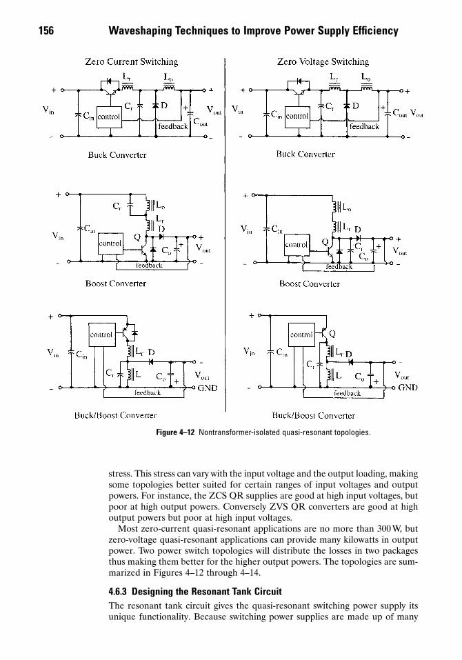
stress. This stress can vary with the input voltage and the output loading, makingsome topologies better suited for certain ranges of input voltages and outputpowers. For instance, the ZCS QR supplies are good at high input voltages, butpoor at high output powers. Conversely ZVS QR converters are good at highoutput powers but poor at high input voltages.
Most zero-current quasi-resonant applications are no more than 300W, butzero-voltage quasi-resonant applications can provide many kilowatts in outputpower. Two power switch topologies will distribute the losses in two packagesthus making them better for the higher output powers. The topologies are sum-marized in Figures 4–12 through 4–14.
4.6.3 Designing the Resonant Tank CircuitThe resonant tank circuit gives the quasi-resonant switching power supply itsunique functionality. Because switching power supplies are made up of many
156 Waveshaping Techniques to Improve Power Supply Efficiency
Figure 4–12 Nontransformer-isolated quasi-resonant topologies.
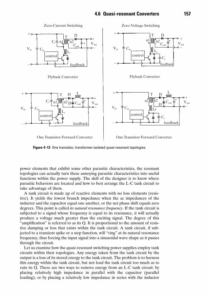
power elements that exhibit some other parasitic characteristics, the resonanttopologies can actually turn these annoying parasitic characteristics into usefulfunctions within the power supply. The skill of the designer is to know whereparasitic behaviors are located and how to best arrange the L-C tank circuit totake advantage of them.
A tank circuit is made up of reactive elements with no loss elements (resis-tive). It yields the lowest branch impedance when the ac impedances of theinductor and the capacitor equal one another, or the net phase shift equals zerodegrees. This point is called its natural resonance frequency. If the tank circuit issubjected to a signal whose frequency is equal to its resonance, it will actuallyproduce a voltage much greater than the exciting signal. The degree of this“amplification” is referred to as its Q. It is proportional to the amount of resis-tive damping or loss that exists within the tank circuit. A tank circuit, if sub-jected to a transient spike or a step function, will “ring” at its natural resonancefrequency, thus forcing the input signal into a sinusoidal wave shape as it passesthrough the circuit.
Let us examine how the quasi-resonant switching power supplies employ tankcircuits within their topologies. Any energy taken from the tank circuit by theoutput is a loss of its stored energy to the tank circuit. The problem is to harnessthis energy within the tank circuit, but not load the tank circuit too much as toruin its Q. There are two ways to remove energy from an L-C tank circuit: byplacing relatively high impedance in parallel with the capacitor (parallelloading); or by placing a relatively low impedance in series with the inductor
4.6 Quasi-resonant Converters 157
+
–
Vin Cin
control
Cr n1 n2
Cout
++
–Vout
Lr
feedback
Flyback Converter
+
–
Vin Cin
+
–
Vin
+
–
Vin
Flyback Converter
Cin
Cr n1 n2 D
D+
–Vout
controlLr
feedback
Cin
controlCr
Lr
n2n1
T D L
Cout Vout
+
–
feedback
One Transistor Forward Converter One Transistor Forward Converter
T
Cout
L
control
n1T D
n2Cout
Lr
Cr
feedback
D
Zero-Current Switching Zero-Voltage Switching
T+ +
–
+ +
D
Vout
Figure 4–13 One transistor, transformer-isolated quasi-resonant topologies.

(series loading). This leads to quasi-resonant “subspecies”: series-resonant, zero current (or voltage) quasi-resonant switching power supplies and parallel-resonant zero current (or voltage) quasi-resonant switching power supplies.They differ in how they load the resonant tank circuit and can be seen in Figure4–15.
Let us examine how one determines the values of the inductor and capacitor. Several assumptions have to be made at the beginning of the designprocess since several of the tank circuit’s characteristics are variable within theapplication. The first is to assume a value for the Q of the tank circuit. In theapplication, the Q varies greatly with the amount of load placed on the outputof the supply. So, a good value to start with is
Qest = 5
Next, decide the natural resonance frequency of the tank circuit. For the avail-able quasi-resonant controller ICs on the market, the range is between 1 and 2MHz. This limit should be considered the maximum limit within conven-tional QR designs. So 1 to 1.5MHz is a typical choice. Lower frequencies canbe used and some efficiencies can be gained. The equation for the resonancefrequency is
158 Waveshaping Techniques to Improve Power Supply Efficiency
+
–
VinCin
control
+
–
VinCin
control
Lo
Cout
Lr
XF
Q1
Q2
n2
n1Cr
feedback
C
C
+
–Cout
+
feedback
n2
Cr
n1
C
C
Hald-Bridge Hald-Bridge
+
–Vout Vout
+
Lo
Cout
+
–Vout
+B
XF
Lr
CrQ2 Q4
Q1 Q3XF
+
–
VinCin
control
feedback
+
–
Vin control
XF
Q1Q2
B
T
Cr
2Cr
2
Q3
Q4
XF
+
–Vout
Cout
Lo
feedback
XF
TQ1
Q2
B
Lo
TLr
TLr
Zero Current Switching Zero Voltage Switching
B
Cin
+
Figure 4–14 Two or more transistor, transformer-isolated quasi-resonant converters.
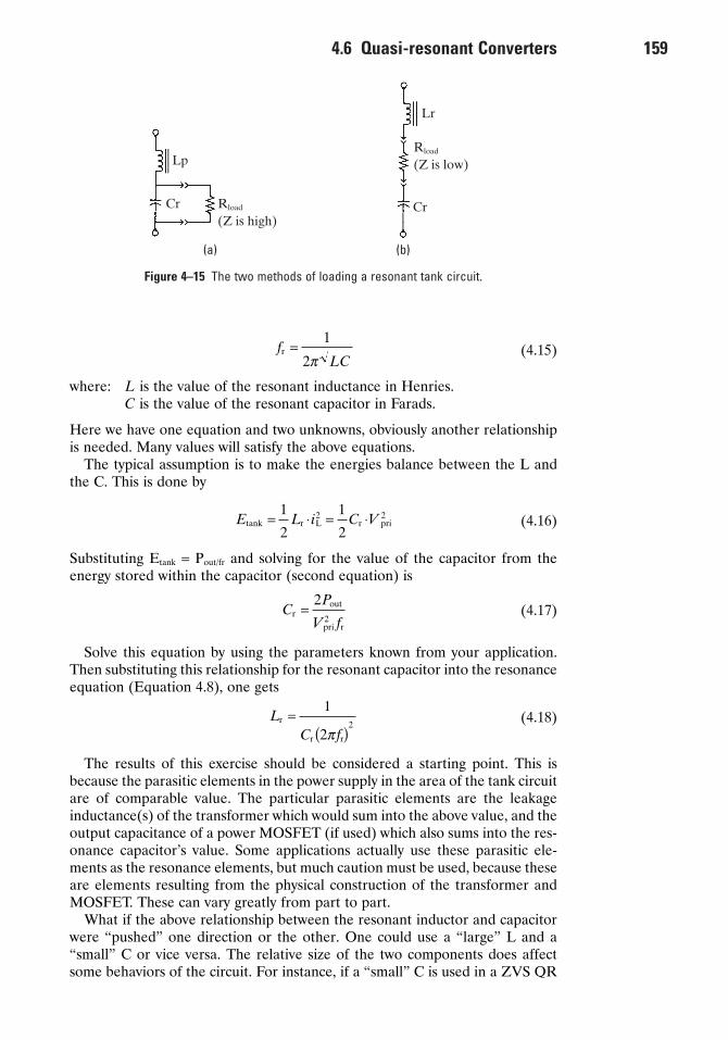
(4.15)
where: L is the value of the resonant inductance in Henries.C is the value of the resonant capacitor in Farads.
Here we have one equation and two unknowns, obviously another relationshipis needed. Many values will satisfy the above equations.
The typical assumption is to make the energies balance between the L andthe C. This is done by
(4.16)
Substituting Etank = Pout/fr and solving for the value of the capacitor from theenergy stored within the capacitor (second equation) is
(4.17)
Solve this equation by using the parameters known from your application.Then substituting this relationship for the resonant capacitor into the resonanceequation (Equation 4.8), one gets
(4.18)
The results of this exercise should be considered a starting point. This isbecause the parasitic elements in the power supply in the area of the tank circuitare of comparable value. The particular parasitic elements are the leakageinductance(s) of the transformer which would sum into the above value, and theoutput capacitance of a power MOSFET (if used) which also sums into the res-onance capacitor’s value. Some applications actually use these parasitic ele-ments as the resonance elements, but much caution must be used, because theseare elements resulting from the physical construction of the transformer andMOSFET. These can vary greatly from part to part.
What if the above relationship between the resonant inductor and capacitorwere “pushed” one direction or the other. One could use a “large” L and a“small” C or vice versa. The relative size of the two components does affectsome behaviors of the circuit. For instance, if a “small” C is used in a ZVS QR
LC f
r
r r
=1
( )22
p
CP
V fr
out
pri r
=2
2
E L i C Vtank r L r pri= ◊ = ◊1
2
1
22 2
fLC
r =1
2p
4.6 Quasi-resonant Converters 159
Lp
Rload
(Z is high)Cr
(a)
Lr
Rload
(Z is low)
Cr
(b)
Figure 4–15 The two methods of loading a resonant tank circuit.

supply the peak ring voltage will increase thus producing a higher voltage stresson the power switch. Inserting the desired limiting voltage value into Equation4.17 and solving will adjust the estimated capacitor value to achieve thismaximum voltage. In typical 1 to 1.5MHz QR applications the range of valuesfor the tank elements are
Cr � 7,000 to 10,000pF
Lr � 2 to 5uH
Another arrangement for the tank circuit in ZCS QR supplies takes advan-tage of the leakage inductances of the primary and secondary(ies). The designercan “push” the resonant capacitor through the transformer and place it on thesecondary as seen in Figure 4–16. This is done by utilizing the equation thatdescribes the reflection of impedances through a transformer.
(4.19)
Substituting the value of the resonant capacitor (across the primary winding)for Zpri one can determine the value needed on the secondary of the trans-former. Without “pushing” the capacitor through the transformer, inductivevoltage spikes still are present on the primary during transitions. When the resonant capacitor “pushed” through the transformer, the leakage inductancesare summed into the resonant inductor and their dv/dts are now controlled bythe tank circuit and the voltage spikes disappear. This eliminates the need forsnubbing across the primary winding and will improve the RFI behavior of thesupply.
If the transformer has multiple secondaries, the ZCS resonant capacitor canbe split and placed on each secondary or can be placed across the entire sec-ondary winding if an autotransformer secondary arrangement is used as shownin Figure 4–17.
If multiple isolated secondaries are used, one might split the values of thesecondary resonant capacitors in proportion to the respective output powers.That is
(4.20)CP
P
n
nCr n
0 n
0 total
sec n
pri
r pri( )( )
( )
( )( )ª
ÊËÁ
ˆ¯ÊËÁ
ˆ¯
◊2
Zn
nZsec
sec= ÊËÁ
ˆ¯
◊pri
pri
2
160 Waveshaping Techniques to Improve Power Supply Efficiency
Transfomer D+Vin
Cr
Lr
Q
GND
np
L1(p)
nsL1(s) Co
+
–
Vout
Transfomer D+Vin
Lr
Q
GND
np
L1(p)
nsL1(s) Co
+
–Vout
Cr
(a)
¢
(b)
Figure 4–16 “Pushing” the resonant capacitor through a transformer in ZCS QR supplies: (a)primary-side resonance; (b) secondary-side resonance.
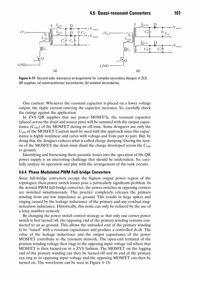
One caution: Whenever the resonant capacitor is placed on a lower voltageoutput, the ripple current entering the capacitor increases. So, carefully checkthe ratings against the application.
In ZVS QR supplies that use power MOSFETs, the resonant capacitor(placed across the drain and source pins) will be summed with the output capac-itance (COSS) of the MOSFET during its off-time. Some designers use only theCOSS of the MOSFET. Caution must be used with this approach since this capac-itance is highly nonlinear and varies with voltage and from part to part. But, bydoing this, the designer reduces what is called charge dumping. During the turn-on of the MOSFET, the drain must shunt the charge developed across the COSS
to ground.Identifying and harnessing these parasitic losses into the operation of the QR
power supply is an interesting challenge that should be undertaken. So, care-fully analyze its operation and play with the arrangement of the tank circuits.
4.6.4 Phase Modulated PWM Full-bridge ConvertersSince full-bridge converters occupy the highest output power region of thetopologies, their power switch losses pose a particularly significant problem. Inthe normal PWM full-bridge converter, the power switches in opposing cornersare switched simultaneously. This practice completely releases the primarywinding from any low impedance ac ground. This results in large spikes andringing caused by the leakage inductance of the primary and any residual mag-netization inductance. Historically, this noise can only be reduced by the use ofa lossy snubber network.
By changing the power switch control strategy so that only one corner powerswitch is first turned off, the opposing end of the primary winding remains con-nected to an ac ground. This allows the unloaded end of the primary windingto be “tuned” with a resonant capacitance and produce a controlled dv/dt. Thevalue of the leakage inductance and the output capacitance of the powerMOSFET contribute to the resonant network. The open-end terminal of theprimary winding voltage then rings to the opposing input voltage rail where thatMOSFET is then turned-on in a ZVS fashion. The MOSFET on the laggingend of the primary winding can then be turned off and its end of the primarycan ring to its opposing input voltage and the opposing MOSFET can then beturned on. The waveforms can be seen in Figure 4–18.
4.6 Quasi-resonant Converters 161
T
+Vin
GND
Q
Lr
L1(s)
L1(s)
D
Dnp
L1(p)Cr Co
Co2
+Vout(2)
+Vout(1)
+Vin np
L1(p)
Lr
Q
GND
L1(s1)
Cr
D
Co
Co2
D+Vout(2)
+Vout(1)
–
–
Cp
(a) (b)
T
¢ ¢
L1(s2)
¢
¢¢
Figure 4–17 Second-side resonance arrangements for complex secondary designs in ZCSQR supplies: (a) autotransformer secondaries; (b) isolated secondaries.

Since both ends of the primary winding have a single-ended loaded windingduring their respective turn-off transitions, each of the MOSFETs accomplishZVS turn-off. The output rectifiers gain some efficiency since their current tran-sitions appear more zero-current switching in nature.
There are control ICs presently in the market. This is one technique toincrease the frequency of full-bridge converters and gain three to five percentin efficiency over the normal PWM full-bridge converters. The cost of the supplydoes increase since more gate drive transformers are required.
162 Waveshaping Techniques to Improve Power Supply Efficiency
Lo
Cout+B
+
–
Vout
XFD
CB
AXF
control
+Vin
feedback
Gat
e A
Gat
e B
Gat
e C
Gat
e D
ConductionB-D
ConductionA-C
Vdiode(D)
+Vin
D is turned on
Von(C)
C is turned off
T
Figure 4–18 Phase modulation of a PWM full-bridge converter.

4.7 High Efficiency Design Examples
The following design examples contain various techniques to improve theoverall efficiency of common designs. Most of the designs of active clamps andlossless snubbers are empirical, so they are not included within these designexamples.
Care must be taken in using the new techniques because of the patents thatcover many of their uses. There may be a licensing fee that needs to be paiddirectly to the patent holder or a small per-piece fee that is paid when buyingthe control IC. Please investigate this before introducing these power suppliesto production.
4.7.1 A 10 Watt Synchronous Buck ConverterApplicationThis design example is a redesign of the PWM design example 1 that shows howone would include synchronous rectifiers (Section 3.15.1).
In designing a synchronous switching power supply, one must be very carefulwhen choosing the control IC. For the sake of maximizing efficiency and mini-mizing space, the average synchronous controllers take many liberties in systemoperation, which make them only good for the IC supplier’s mentioned appli-cation. Many subtleties of operation cannot be determined unless the datasheetis read completely. For instance, every time I attempt to design a synchronousconverter and try to use off-the-shelf ICs, I throw out three to four designs. Thisis because I encounter an unexpected operational mode that cannot be over-come or modified because the function is not brought out to a pin. Needless tosay, it is a frustrating process if one wants something different from the “cookiecutter” solution (refer to Figure 4–20 for the schematic).
Design specification
Input voltage range: +10V to +14VDCOutput voltage: +5.0VDCRated output current: 2.0AOvercurrent limit: 3.0AOutput ripple voltage: +30mV p-pOutput regulation: +/- 1%Maximum operating temperature: +40°C
“Black box” predesign estimates
Output power: (+5.0V)(2A) = 10.0W (max)Input power: Pout /Est. Effic. = 10.0W/0.90 = 11.1WPower switch loss: (11.1 - 10W)(0.5) = 0.5WCatch diode loss: (11.1 - 10W)(0.5) = 0.5W
Input average currents
Low input: (11.1W)/(10V) = 1.11AHigh input: (11.1W)/(14V) = 0.8AEstimated peak current: 1.4 (Iout(rated))
1.4(2.0A) = 2.8A
The desired frequency of operation is 300kHz.
4.7 High Efficiency Design Examples 163

Inductor design (refer to Section 3.5.5)The worst case operating condition is at the high input voltage.
where: Vin(max) is the maximum possible input voltage.Vout is the output voltage.Iout(min) is the lightest expected load current.fsw is the operating frequency.
The inductor is to be a surface mount toroid on a J-leaded plastic mountingboard. There are standard surface mount inductors available from many sup-pliers. I have chosen the part DO3340P-333 from Coilcraft (33mH).
Selection of the power switch and synchronous rectifier MOSFETs
Power switch. The power switch is going to be a transformer-coupled N-channelpower MOSFET. I plan to use a dual N-Channel MOSFET in an SO-8 packageto help save on PCB space. The maximum input voltage is 14 VDC. Therefore,a VDSS rating of +30VDC or higher will be satisfactory. The peak current is 2.8A.
The first step in the selection process is to determine the maximum RDS(on)
for the desired MOSFETs. This is done by examining the thermal model (seeAppendix A). The maximum RDS(on) is found by
It is also desired to keep the heat dissipation less than 1W for the device so theestimated RDS(on) should be less than
I will select the FDS6912A dual N-channel MOSFET with an on-resistance of28 milliohms at a VGS of 10V packaged in an SO8 package.
Synchronous Diode. A Schottky diode about 30 percent of the rating of the con-tinuous rating of the synchronous MOSFET needs to be placed in parallel withthe MOSFET’s intrinsic diode. This would be about 0.66A at 30V. I will use anMBRS130. This diode produces a 0.35V forward voltage drop at 0.66 A.
Alternate choice. Fairchild Semiconductor, at the time of writing this book,released an integrated Schottky diode and MOSFET where the parallel Schottky diode is placed directly on the MOSFET silicon die (SyncFET). The SyncFET has a 40 milliohm N-channel MOSFET, copackaged with a 28milliohm SyncFET. The part number is FDS6982S.
The output capacitor (refer to Section 3.6)The value for the output capacitor is determined by the following equation”
R P IDS on max D est pk est
W A milliohms max. each MOSFET
-( ) ( ) ( )= ( )= ( ) ( ) < ( )
2
21 2 8 127.
R T T I RDS on max j max amb max D JA( )( ) ( ) ( )= -[ ] ( ) ( )[ ]2
Lmin. .
.--( ) -( )( )( )
=14 5 1 5 14
1 4 0 5 30027 5
V V V V
A kHzHm
LV V V V
I fmin
in max out out in max
out min sw
--( ) -( )( ) ( )
( )
1
1 4.
164 Waveshaping Techniques to Improve Power Supply Efficiency

The major concern of both output and input filter capacitors is the ripplecurrent entering the capacitor. In this application, the ripple current is identi-cal to the inductor ac current. The maximum limits of the inductor current is2.8A for I peak and about one-half the maximum output current or 1.0A. Sothe ripple current is 1.8 A p-p or an estimated RMS value of 0.6 A (about one-third of the p-p value).
I will be using a surface mount tantalum capacitor because they typicallyexhibit about 10 to 20 percent of the ESR of electrolytic capacitors. I will alsoderate the rating of the candidate capacitors by 30 percent at +85°C ambienttemperature.
The best candidate capacitors are from AVX. They have very low ESR andthus can handle very high levels of ripple current. These capacitors are excep-tional. I will place two pieces of the following parts in parallel on the output.
AVX:TPSE107M01R0150 100mF (20%), 10V, 150mohm, 0.894 Arms
TPSE107M01R0125 100mF (20%), 10V, 125mohm, 0.980 Arms
Nichicon:F751A107MD 100 mF (20%), 10V, 120mohms, 0.92Arms
The input filter capacitors (Sections C.1 and C.2)This capacitor experiences the same current waveform at the power switch,which is a trapezoid with an initial current of about 1A rising to 2.8A with verysharp edges. This capacitor has much more rigorous operating conditions thanthe output filter capacitor. I will estimate the RMS value of the trapezoidalcurrent waveform as a piecewise superposition of two waveforms: a rectangu-lar 1A peak waveform and a triangular waveform with a 1.8A peak. This yieldsan estimated RMS value of 1.1A.
The value of the capacitor is then calculated as
Capacitors at the higher voltages have smaller capacitance values. There will betwo 100mF capacitors in parallel. The candidates are
AVX (two required per system):TPS107M020R0085 100 mmF (20%), 20V, 85mohms, 1.534Arms
TPS107M020R0085 100 mF (20%), 20V, 200mohms, 1.0Arms
Selecting the controller IC (U1)The desired features one might look for in a buck controller IC are:
1. Ability to operate directly from the input voltage.2. Pulse-to-pulse overcurrent limiting.3. Totem-pole MOSFET drivers.
CP
f Vin
in
sw ripple p-p
W
kHz=
( )=
( )( )( )2 2
11 1
300 0 5
.
.
CI DC
f V
C
out minout max min
sw ripple p-p
out minA V V
kHz mVF
( )( ) ( )
( )
( )
--( )
( )
-( ) -( )( )( )
=
1
2 1 5 14
300 30142 m
4.7 High Efficiency Design Examples 165

4. Some control over the delay between the power switch and the synchro-nous rectifier MOSFETs.
There are very few synchronous buck controllers on the market that are nottargeted to the +5 to 1.8V microprocessor local regulator application (i.e., Vdd
of +12V, and Vin of +5V). Also ICs that bring out enough functions to pins sothat one may tailor its performance to the application. I threw out two entireproduct offerings from two major California companies (not to throw stones)and found only one part that fits my needs, the UC3580–3 from Unitrode/TI.
The internal reference presented to the voltage error amplifier is 2.5V +/-2.5 percent.
Setting the frequency of operation (R7, R8, and C8)R8 charges the timing capacitor (C8) and R7 discharges the timing capacitor.First, one decides the maximum duty cycle of the converter. Since the outputvoltage is about 50 percent of the lowest input voltage, I will choose a 60 percentmaximum duty cycle. From the data sheet:
or
R8 = 1.875 ◊R7
The charge time is 0.6/300kHz or 2mS maximum on time. The parametertables use a timing capacitor value of 100pF which is fairly small and will notdissipate much energy. I will use this value. The value of R8, therefore, is
The volt-second limiter (R4 and C5)This IC has a method of feed-forward maximum pulsewidth limiting. As theinput voltage increases, the expected operating pulsewidth of the buck converterdecreases. An R-C oscillator is directly connected to the input voltage and itstimeout is inversely proportional to the input voltage. Its timeout period is setto about 30 percent longer than the excepted operating pulsewidth. If the passunit is still conducting at the moment that the volt-second oscillator times out,the pass unit is cutoff.
I am selecting C5 to also be 100 pF since its timing is about the same fre-quency as the oscillator. That makes R4 around 47Kohms.
Setting the deadtime between the pass unit and the synchronous rectifier MOSFETsOne could perform the turn-on and turn-off delay calculations presented inSection 3.7.2 and still have to adjust the value of the deadtime delay-settingresistor (R6) at the breadboard stage. A starting value of 100 nS is good. Thetypical MOSFET turn-on delay is about 60 nS. The 100 nS will assure that thereis no push-through current.
The IC produces an asymmetrical deadtime delay. From the graph in thedatasheet a value of 100 kohms will produce a pass unit turn-on delay of about110nS and a turn-off delay of 180nS.
I am fully planning to reduce these delays at the breadboard stage. Delaysthis long cause the diodes to conduct too long, thus causing the losses to behigh. But this is operating on the safe side.
R
R
8 2 0 100 20
7 20 1 875 10 66 12
= ( ) ( ) =
= ( ) =
.
. .
mS pF k ohms
k k make k
max .duty cycle = +( )R R R8 8 1 25 7
166 Waveshaping Techniques to Improve Power Supply Efficiency

Design of the gate drive transformer (T1)The gate drive transformer is a very simple 1 : 1 turns ratio forward-mode trans-former. There are not extraordinary demands being placed on the transformersince it is a very low power, ac-coupled (bipolar flux), 300kHz transformer.
A ferrite toroid about 0.4 inches (10 mm) is sufficient, such as TDK partnumber K5T10x2.5x5 (Bsat is 3300G), or Philips part number 266T125–3D3 (Bsat
is 3,800G).From Section 3.5.3, the number of turns to produce 1,000G (0.1T) or 0.3 Bsat
is
= 16.6 turns round up to 17 turns
The gate drive transformer will be bifilar wound where two identical wires(about #30AWG) will be wound simultaneously with equal turns. For conve-nience, the transformer will be mounted on a four-pin, gull wing, surface mountheader.
Current sense resistor (R15) and voltage sensing resistor divider (R11 and R13)The IC provides only a shutdown pin with an activation threshold of 0.4Vminimum. I plan to enter a hiccup mode of overcurrent protection as a form ofback-up protection. To minimize the size of the current sensing resistor, I willemploy a variation of the current foldback sensing circuit. Here 0.35 V will becontributed by a resistor in the voltage sensing resistor divider (R14). The valueof R15 is then
The Dale resistor is WSL-2010-.02–05.I will assign a sense current of about 1.0mA through the voltage sensing resis-
tor divider. This make the resistance represented by the sum of R13 and R14
R14 is then
R13 then becomes
2.5k - 360ohms = 2.14kohmsmake 2.15kohms 1 percent tolerance.
R11 is then
make 2.49k ohms 1%
Compensating the voltage feedback loop (refer to Appendix B)This is a voltage-mode, forward converter. To produce the best transient responsetime, a two-pole, two-zero method of compensation is going to be used.
R11 5 0 2 5 1 2 5= -( ) =. . .V V mA k
R15 0 35 1 0 350= =. .V mA ohms make 360 ohms
Rsum V mA k= =2 5 1 0 2 5. . .
R15 0 05 3 16 6= =. .V A mohms make 20 mohms
N =( )
( )( )( )
12 10
4 300 1 000 0 06
8
2
V
kHz G cm, .
NV
f B Apri
in nom
C
=◊ ◊ ◊
( )10
4
8
max
4.7 High Efficiency Design Examples 167

Defining the control-to-output characteristicThe output filter pole is determined by the filter inductor and capacitor and isa -40dB/decade rolloff. Its nominal corner frequency is
(3.58)
The zero caused by the output filter capacitor(s) (ESR is two 150mohms in parallel) is
The intrinsic absolute gain of the power circuit at dc is
Locating the compensating poles and zeros of the error amplifierI shall use a gain cross-over frequency of 15kHz, which is quite satisfactory forthe majority of applications. This yields a transient response time around 200mS.
fxo = 15kHzFirst one assumes that the final closed loop compensation network will have
a continuous -20dB/decade slope. To achieve a 15kHz cross-over frequency theamplifier must add gain to the input signal and “push-up” the gain curve of theBode plot.
This is the gain needed at the midband plateau (G2) to achieve the desiredcross-over frequency.
The gain exhibited at the first set of compensating zeros is
To compensate for the double filter pole, I will place two zeros at one-halfthe filter pole frequency:
fez1 = fez2 = 980Hz
The first compensating pole will be located at the capacitor’s ESR frequency(4,020Hz):
fep1 = 10,610Hz
The second compensating pole is just used to maintain high-frequency stabilityby depressing the gain above the cross-over frequency:
fep2 = 1.5 fxo = 22.5kHz
Now one can begin calculating the component values within the error ampli-fier. Refer to Figure 4–19.
G G f f
G
A
1 2 20 4 1 20 980 10 6101 16 5
= + ( ) = + ( )= -
( )
Log dB+ Log Hz HzdB
1=0.15 absolute gain
ez2 ep1 . ,.
G f f G
G G
A A
xo xo fp DC
xo
xo
Log Log kHz Hz dBdB
= 2=1.6 absolute gain
= ( ) - = ( ) -= = +
( )
20 20 15 1 959 13 62 4 1
, ..
A V V
G A
DC in error
DC DC
V V
Log dB
ª = ( ) ( ) =
= ( ) =
D 14 2 9 4 8
20 13 6
. .
.
fR C
esr
esr o m FHz= =
( )( )=
1
2
1
2 75 20010 610
p p m,
fpH F
Hz=( )( )
=1
2 33 2001 959
p m m,
fs L C
p
o oˇ=
1
2
168 Waveshaping Techniques to Improve Power Supply Efficiency

C13 = 0.0026mF make 0.0027mF
R10 = (A1)(R11) = (0.15)(2.59kW) = 373W make 360W
Cf R z
121
10
1
2 10 610 360=
( )( )=
( )( )2 Hz ˇez1p p ,
C
f A R13
1
2 2 11
1
2 15 1 6 2 49=
( )( )( )=
( )( )( )p pxo kHz kz. .
4.7 High Efficiency Design Examples 169
(b)
Control-to-Output0
- 90
- 180
- 360
- 270
0.1 1 10 100 1 k 10 k 100 k 1 M
Error Amp
Closed Loop
Frequency (Hz)
Pha
se (
Deg
rees
)
+ 80
+ 60
+ 40
+ 20
0
- 20
- 40
- 60
0.1 1 10 100 1 k 10 k 100 k 1 MFrequency (Hz)
(a)
Control-to-Output
Closed LoopError Amp
fxo
Gai
n (d
B)
Figure 4–19 The gain and phase Bode plots for design example 4.7.1: (a) the gain plot for thesynchronous buck converter; (b) the phase plot for the buck synchronous converter.

C12 = 0.042mF make 0.05mF
R12 = R10/A2 = (360W)/(1.6) = 225W make 220W
C10 = 0.31mF make 0.33mF
4.7.2 A 15 Watt, ZVS Quasi-resonant, Current-mode Controlled Flyback ConverterThis design is a novel turn about to the traditional voltage-mode controlled ZVSquasi-resonant converters. By modifying a conventional, non-duty cycle limitedcurrent-mode control IC into fixed off-time, current-mode controlled on-timemethod of control, a ZVS topology can be created. The added advantage ishaving the overcurrent protection and responsiveness of current-mode whilehaving the reduced switching losses of a resonant technology. Although its fre-quency of operation may not exceed 1 MHz, it does offer the advantages of noswitching losses and reduced EMI radiation. Please refer to Figure 4–22 for theschematic.
Design specification
Input voltage range: 18V to 32VDC, +24VDC (Nominal)Output voltage: +15VDC @ 0.5A to 1ALow voltage “no start” voltage: 8.0V +/- 1.0V
Cs f R s z
101
2 12
1
2 22 5 220=
( )( )=
( )( )ˇ ˇ kHz ˇez2 .
170 Waveshaping Techniques to Improve Power Supply Efficiency
+Vin
C1100uF20V
GND
100uF20V
C3.1uF
Q1
R1
D11K
T1Q2
R2
1K
L2
L1
C9 C10
D2
R11FB
R12C11
+Vout
R13
R14
R15GND
PGND
C4.1 uF
4
3
2
9
1
R3
R5R4
C5
R6
C6 C714 15
6 5
DR1DR2 PGND
VDDU1
comp
EAin
UC3580-3
Line SHTDWN
OSC1
OSC2
AGNDSS
VSrmp
DLYREF
12
13
16
11
10
AGND
C8
R8
R7
C13R9
C12 R10
C2
Figure 4–20 A 10 watt synchronous buck converter.

Predesign “black box” considerations
Output power: Vout ◊ Iout = (15V)(1A) = 15 WattsMaximum peak current:
Input average currents:
Determining the gauge wire needed on the primary, the supply is required tooperate at 18V at the rated load current, so the primary wire gauge needs tobe equivalent to #20AWG.
Designing the flyback transformerThe transformer is going to be the only nonsurface mount component insidethe power supply because there is no surface mount core style large enough tosupport 15W. A toroid will work but I will be using a low profile E-E core fromTDK. The “EPC” style of low profile cores will do.
Determining the core material. The power supply will be operating over the fre-quency range of around 150kHz to 500 kHz, which is an area where two typesof core material could be used. The “F”, “3C8”, and “H7P4” (similar materialsmade by different manufacturers) are useable up to about 800 kHz. The “N”,“3C85”, and “H7P40” are useable into the MHz region, with slightly lower corelosses in this operational region. For this application, I will use the H7P40 mate-rial (TDK).
Determining the core size. TDK rates its cores by the amount of power that canbe handled by the core in a one-transistor forward converter. Its volume require-ments are very similar to a flyback converter. The EPC core that rated at 15 Wor greater is the EPC 17 core size. The part numbers for this assembly are: core,PC40EPC17-Z; bobbin,BER17–1111CPH; and clamp, FEPC17-A.
Determining the primary inductance. I am assigning a maximum on-time of 7 uS,which would occur at the minimum input voltage. The primary inductancewould then be
The length of the air-gap should be approximately
lLI
A Bgap
pk
c max
H A
cmcm
ª
=( )( )
( )( )=
0 4 10
0 4 27 4 6 10
0 22 1800101
2 8
2
28
22
.
. .
..
p
p m
LV T
Ipri
in min on max
pk
V 7 S
AH
=
=( )( )
( )=
( ) ( )
18
4 627 3
mm
..
IP
eff V
IP
eff V
in avout
in nom
in av hiout
in low
W
VAmps
W
VAmps
( )( )
-( )( )
ª◊
=( )
=
ª◊
=( )
=
15
9 240 7
15
9 180 926
.
.
IP
Vpk
out
in min
W
VAmpsª
◊=
( )=
( )
5 5 5 5 15
184 6
. ..
4.7 High Efficiency Design Examples 171

The AL of the core with this air-gap is about 55nH/N2. This AL is the versionused by TDK and uses the following equation to determine the number of turns:
The secondary winding’s inductance controls how quickly the core would emptyitself of the stored energy for the discontinuous-mode of operation. Since theinput and output voltages are very close in magnitude, a 1 :1 turns ratio wouldbe possible. This would result in a 3mS off-time within a comparable PWMsystem. Let us use a 1 :1 turns ratio; it could be bifilar wound to promote thetightest coupling.
Nsec = 22 turns
Wire gauges
Primary: #20AWG or equivalent—make 3 strands of #24AWGSecondary: #20AWG or equivalent—make 3 strands of #24AWG
To reduce confusion, I will use two differently colored wires.
Transformer winding techniqueThe primary and secondary windings will be twisted together prior to windingthem onto the bobbin. The windings will be separated on each end (distin-guished by the colors) and soldered to the assigned terminals. A layer of Mylartape will be placed on the exterior surface for aesthetics and safety.
Designing the resonant tank circuitThis is a first-pass estimate for the values of the tank circuit since at this timeit is impossible to predict the influences of all the parasitic elements that wouldoccur in the physical circuit. Readjustment of calculated tank values and the off-time setting on the controller IC will be necessary at the breadboard stage.
First one assumes that the power stored within the L-C tank circuit will beshared equally, or that
Rearranging and solving for the resonance capacitor value,
I wish to limit the peak voltage across the resonant capacitor (C7) to less than100V and solve
I have chosen the maximum operating frequency of the power supply to be 250kHz. At light loads, the maximum on-time should be in the order of 10 to15 percent. So, the resonance frequency will be around 250kHz as well. Solvingfor the resonant inductor,
Cr 2
2 15W
70 V 250kHz0.024 F,make .02 F=
( )
( ) ( )= m m
CP
V fr
out
C op
=◊
22
P
f
C V L iout
op
r c r L= =2 2
2 2
N
L
Apri
pri
L
27 H
55 Hturns, make 22 turns= = =
m
m22 2.
172 Waveshaping Techniques to Improve Power Supply Efficiency

Designing the output rectifier/filter stage
Selection of the output rectifier
Let us select the MBR360 for D4.
Calculating the needed output filter capacitor
make C8 equal 47mF at 25VDC. I will use a very good grade tantalum capaci-tor and place in parallel a 0.5mF ceramic capacitor.
Designing the bootstrap start-up sectionI will be using the current limited linear regulator type of start-up circuit.
For R1, the base bias resistor,
For R2, the collector current limiting resistor,
Design of the controller sectionI will be using a garden variety UC3842 current-mode control IC. The IC selec-tion is important because it cannot have 50 percent duty cycle limiting. Theoscillator will be operating as a fixed off-time one-shot, which means shortingthe timing capacitor to ground and the on-time is then only controlled by thecurrent sense input pin. When appropriate current is achieved, then the timingcapacitor will be release and the oscillator will operate like a one-shot timer forthe off-time and restart the next on cycle.
Modifying the controller to fixed off-time. This is done by placing a small signalN-channel MOSFET across the timing capacitor. The gate is connected to thegate of the main power MOSFET. A couple of good choices for the small signalMOSFET is the BS170 or 2N7002. By referring to the data sheet for the timingelements and needing an off-time of approximately 2 mS, means that the timingcomponents will be approximately 15Kohms for the timing resistor and 220pFfor the timing capacitor. These values will be adjusted to match the resonanthalf-period of the tank circuit during the breadboard stage.
R2 18 13 10 500= -( ) ( ) =V V mA ohms make 510 ohms
R1 18 12 0 5 12= -( ) ( ) =V V mA K.
CI T
Vo
out max off
ripple
A S
mVF
=
=( )( )
=
( )
1 2
5040
mm
V VN
NVr out
pri
in max
15V 32 V 47 V
= + ( )
= + =
( )sec
LC f
r
r r
F kHzH
=( )
=( ) ( )( )
=
1
21
02 2 25020
2
2
p
m pm
.
4.7 High Efficiency Design Examples 173

Design of the voltage feedback loopI am going to use a sense current of 1.0mA. This makes the lower resistor inthe voltage sensing resistor divider (R9) a 2.49K 1 percent resistor.
The upper resistor (R8) is
make 12.4K 1 percent.
Designing the feedback loop compensationZero voltage quasi-resonant power supplies usually vary in frequency 4 :1 withvarying input line and load. That variation would make the estimated mini-mum switching frequency at 80kHz. We will need to estimate this for the compensation.
The control-to-output characteristic curves for a current-mode controlledflyback-mode converter, even though it is operating in variable frequency, areof a single-pole nature. So a single pole-zero method of compensation shouldbe used. The placement of the filter pole, ESR zero, and dc gain are
The control-to-output curves can be seen in Figure 4–21.The gain cross-over frequency should be less than fsw/5 or
fxo < 80 kHz/5 < 16kHz
I’ll settle for 10kHz.To determine the amount of gain needed to boost the closed loop function
to 0dB at the gain cross-over frequency (see Equation B.24):
AXO = 18.3 (scaler gain—needed later)
Locate the compensating error amplifier zero at the location of the lowest mani-festation of the filter pole or
Locate the compensating error amplifier pole at the lowest anticipated zero fre-quency caused by the ESR of the capacitor or
f fez fp low Hz= =( ) 112
G f f Gxo xo fp hi DC
dBdB needed for Bode Plot only
= ( ) -= ( ) -= ( )
( )2020 10 000 225 7 725 2
loglog , ..
A
G
f
f
DC
DC
fp hi
fp low
V V
V V
Log dB
V A FHz at rated load 1A
V A FHz at light load 0.5A
=-( )◊
=
= ( ) =
=( )( )
= ( )( )
=( )( )
= ( )( )
( )
( )
28 15
28 2 52 41
20 2 41 7 7
1
2 15 1 47225
1
2 15 0 5 47112
2
..
. .
.
p m
p m
R8 15 2 5 1 12 5= -( ) =V V mA K ohms. .
174 Waveshaping Techniques to Improve Power Supply Efficiency

Knowing the upper resistor in the +5V voltage sensing divider (12.4K),
R A R3 118 3 12 4227 220
== ( )= -
xo
KK round to K
. .
CA R f
31
2 11 2 18 3 12 4 1070
=◊ ◊ ◊
= ( )( )( )=
pp
xo xo
K KHzpF make 68pF
. .
f fep p ESR kHz approximated= = ( )( ) 10
4.7 High Efficiency Design Examples 175
+100
+90
+80
+60
+40
+20
0
–20
–40
–60
Gai
n (d
B)
closed loop
Control-to-Output
error amp
.1 1 10 100 1K 10K 100K
Frequency (Hz)
Control-to-Output0
–90
–180
–270
–360
Error Amp
Closed Loop
Pha
se (
Deg
rees
)
(a)
Frequency (Hz)(b)
.1 1 10 100 1K 10K 100K
Figure 4–21 The gain and phase Bode plots for design example 4.7.1 (compensation design):(a) the gain plot for the power supply; (b) the phase plot for the power supply.
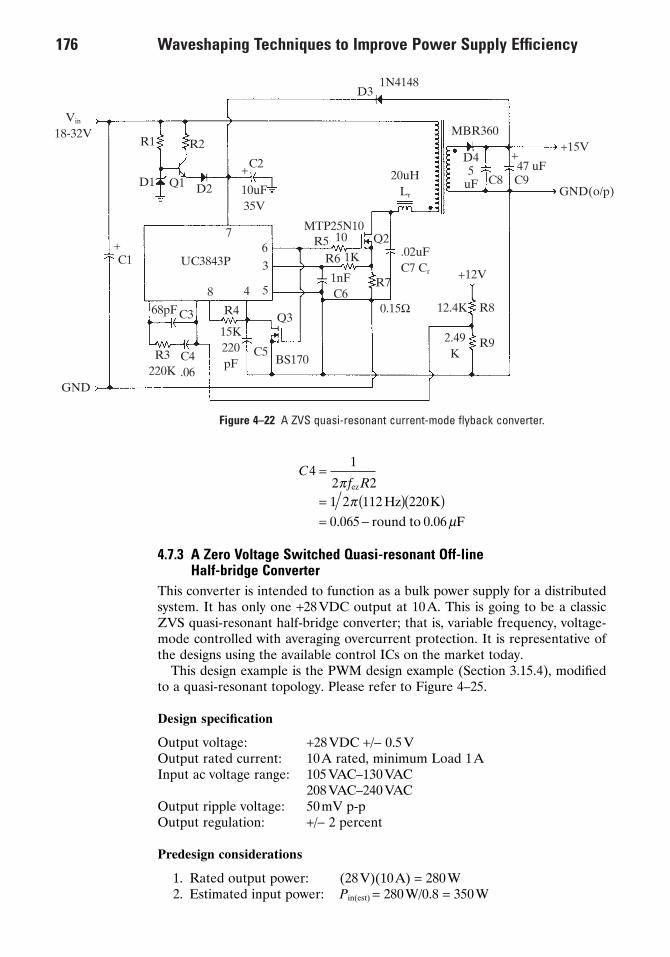
4.7.3 A Zero Voltage Switched Quasi-resonant Off-line Half-bridge Converter
This converter is intended to function as a bulk power supply for a distributedsystem. It has only one +28VDC output at 10A. This is going to be a classicZVS quasi-resonant half-bridge converter; that is, variable frequency, voltage-mode controlled with averaging overcurrent protection. It is representative ofthe designs using the available control ICs on the market today.
This design example is the PWM design example (Section 3.15.4), modifiedto a quasi-resonant topology. Please refer to Figure 4–25.
Design specification
Output voltage: +28VDC +/- 0.5VOutput rated current: 10A rated, minimum Load 1AInput ac voltage range: 105VAC–130VAC
208VAC–240VACOutput ripple voltage: 50mV p-pOutput regulation: +/- 2 percent
Predesign considerations
1. Rated output power: (28V)(10A) = 280W2. Estimated input power: Pin(est) = 280W/0.8 = 350W
Cf R
41
2 21 2 112 2200 065 0 06
=
= ( )( )= -
pp
m
ez
Hz Kround to F. .
176 Waveshaping Techniques to Improve Power Supply Efficiency
Vin
18-32VR1 R2
D1 Q1 D2
+C1
C2+
10uF35V
D31N4148
MBR360
20uHLr
D45
uF C8 C947 uF
++15V
GND(o/p)
+12V
R812.4K
R92.49K
0.15W
.02uFC7 Cr
Q2
R7
MTP25N10R5 10
R6 1K
1nFC6
Q3
BS170C5
R4
15K220pF
UC3843P
76
3
548
68pF C3
R3220K
C4.06
GND
Figure 4–22 A ZVS quasi-resonant current-mode flyback converter.

3. DC input voltages (a voltage doubler is used for 110VAC)a. From 110VAC: Vin(low) = 2(1.414)(90VAC) = 254VDC
Vin(hi) = 2(1.414)(130 VAC) = 368VDCb. From 220 VAC: Vin(low) = 1.414(185VAC) = 262VDC
Vin(hi) = 1.414(270VAC) = 382VDC4. Average input currents (dc):
a. Highest average: Iin(max) = 350W/254VDC = 1.38Ab. Lowest average: Iin(min) = 350W/382VDC = 0.92A
5. Estimated maximum peak current: Ipk = 2.8(280W)/254VDC = 3.1A
This converter is going to be able to pass UL, CSA, and VDE safety require-ments, which will affect the design approach that is taken. It will operatebetween the frequencies of 1MHz at the minimum specified load and no lessthan 200kHz at the maximum specified load.
Design of the transformerI will be using an E-E core with the necessary Mylar tape insulating layers tomeet the isolation requirements of the safety approval agencies. At these oper-ating frequencies, a high-frequency core material will have to be used to mini-mize the core losses at 1 MHz. The material should be the “K” material fromMagnetics, Inc, “3C85” material from Phillips, or “N67” material from Siemans.
One consideration is the variation in the operating flux density over the oper-ating range of the supply. At minimum load (1A) the frequency will be at itshighest (1 MHz), and the Bmax should be about 0.1 Bsat. At maximum load (10 A)the operating frequency is no less than 200 kHz, so its Bmax should be less than0.3Bsat. Let us start by assigning the Bmax at 1MHz at 200G and use this as thereference operation point.
The size of the core will be approximately 1.3 inches (41 mm) on a side. Thiscorresponds to the K-43515 core from Magnetics, Inc. In designing the trans-former, one must keep in mind that the first pulse issued in starting up is at thefull input voltage and the subsequent pulses will be at or closer to one-half ofthe input voltage. To be positive that the core will not enter saturation duringthat first pulse, one limits the maximum Bmax at a higher than normal level:
Checking the maximum operating flux densities using Faraday’s law, at lightload, the frequency is approximately 1 MHz, the Bmax is 211 G. At its heavy load(200kHz) the Bmax is 1,100G. This seems to be exactly what is required.
In calculating the number of secondary turns needed, one needs to considerthat the resonant transition period is approximately 0.5mSec within a 2.5mSecmaximum period per MOSFET at 200kHz. That corresponds to an 84 percentduty cycle. So,
Make 4 turns.
The auxiliary winding should be two turns.
Transformer winding technique (refer to Section 3.5.9)The transformer is going to be wound in an identical fashion as the PWM half-bridge design example (Section 3.15.4). That is, the secondary will be inter-
NsecV V T
V VT=
+( )( )-( )( )
=1 1 2 8 0 5 24
254 2 843 55
. . .
..
Npri
2
V
200KHz 2,200 G .904 cmT=
( )◊
( )( )( )=
382 10
424
8
4.7 High Efficiency Design Examples 177

leaved between two layers of primary windings. The auxiliary winding will beplaced next to the core. Of course the necessary layers of Mylar tape and a 2mm spacing from the side walls of the bobbin are necessary for VDE.
Considerations in the design of the L-C tank circuitIt is desired that the resonance frequency of the tank circuit be 1MHz. In ZVSQR converters, the tank circuit is not responsible for storing and passing onenergy as it is in ZCS QR converters. The tank circuit can be seen more as anoff-time transition shaper similar to a snubber when used in PWM converters.Here a wide range of values for both the inductor and the capacitor will workas long as their combined resonant frequency is 1MHz or
I am planning to use the leakage inductance of the primary as a part of theresonant inductor. For transformers of this nature, a leakage inductance of 0.5to 1uH is typical. I will specify the winding method to the transformer manu-facturer so that the variation in the transformer’s leakage inductance will beheld to a minimum. I will have to add a small inductor external to the trans-former. I will also use the Coss (output capacitance) of the power MOSFET asa portion of the resonant capacitor. This is a highly variable and nonlinearcapacitance and it is difficult to predict its value. The value of the Coss is depen-dent upon the off-time VDSS of the MOSFET, which will be changing duringthe resonant off-time. Obviously, this requires some adjustment during thebreadboard stage.
Just as an estimate, let us calculate the approximate value required for theresonant capacitor.
This value is higher than that exhibited by the output capacitance of theMOSFETs so I will add an external resonant capacitor outside the MOSFET.
Selection of the power semiconductors
1. The power MOSFET (refer to Section 3.4):
VDSS > Vin = 382V make 500V
ID > Iin(av) = 2.75Amps make 4Amps
We can use the MTP4N50E, but the MTP8N50E will result in lower con-duction losses.2. Output rectifier:
VR > 2Vout = 56VDC make > 70VDC
IFWD > Iout(max) = 10Amps, make 20 Amps
Select MBR20100CT
Design of the output filters
1. The minimum ac output filter inductance (refer to Section 3.5.5):
CL f
r =( )
=( ) ( )( )
=
1
2
1
1 2 10 025
2 2
r r H MHzF
p m pm.
fL C
r
r r
=1
2p
178 Waveshaping Techniques to Improve Power Supply Efficiency

Using the LI2 method of determining the size of an MPP toroid, one deter-mines the Magnetics P/N 55206A2 core part number.
The number of turns should be:
The toroid should have an overall wire gauge of #12AWG. We will use 100strand Litz wire to minimize the skin effects.2. The minimum output filter capacitance (refer to Section 3.6):
I will use four capacitors at a value of 47 mF tantalum capacitors. This willmake the RMS ripple current within the ratings of typical capacitors. I willalso place a 0.5 mF ceramic capacitor in parallel with the other capacitors.3. Design the output dc filter choke (refer to Section 3.5.7): Referring to the
permeability versus dc bias graph (Figure 3–22) and selecting a perme-ability that does not excessively degrade at a reasonable dc bias level, Ichoose a permeability of 60 at an “H” level of 40Oe.
Using the same core size as above one gets:
We still need #12AWG wire. Litz wire is easier to wind around a toroid andreduces the skin effect so I will use it.
Design of controller IC related functionsThe MC34067 data sheet contains the necessary equations and graphs in orderto set the critical timer functions of a ZCS QR converter. Some of the times,such as the one-shot off-timer, will have to adjusted in the breadboard stage.
Setting the minimum operating frequencyThe minimum operating frequency of the control IC is set by the combinationof the R and C on the oscillator pin. First one select the oscillator capacitorfrom a graph. The discharge period to produce a 200 kHz period (5 mS) can beproduced with a 200 to 300pF capacitor. Make Cosc = 220pF. The oscillator resis-tor is calculated from
The maximum operating frequency is set by additional discharge current beingdrawn by the error amp through resistor RVFO. The equation to determine theadditional discharge current (Imax) is
I C fmax max. .= ◊ ◊ = ( )( )=
1 5 1 5 220 1330
osc pF MHzAm
RT
Cosc
osc
nS 2.5 S .07 S
0.348 220pFK make 33K
=-
=-( )
( )=
max
.. ,
70
0 34831 7
m m
N =( )( )
( )=
300 5 08
0 4 1012 12
.
..
cm
A turns, make 13 turns
p
Co min
p-p
A S
VF( ) =
( )( )=
10 1
05200
mm
.
NLo turns, make 12 turns= =1 0000085
6811 2,
..
Lo min40 V 28 V 1 S
1.4 1Amp8.5 H( ) =
-( )( )( )
=m
m
4.7 High Efficiency Design Examples 179

The current flowing through the parallel oscillator resistor is
The value of the series discharge resistor (RVFO) from the output of the erroramp to the oscillator is
Setting the one-shot timerThe one-shot timer can be set entirely from a graph and the approximate valuesfrom the graph are RT = 1.5K ohms and the CT = 220pF.
Design of the voltage feedback circuitThe voltage feedback circuit is to be an isolated variety using the error ampli-fier as a noninverting voltage-follower. This is to provide a buffer between theoptoisolator and the VFO. Since this method of quasi-resonant control is a formof voltage-mode control a 2-pole–2-zero form of feedback compensation is nec-essary. The circuit will take the form shown in Figure 4–23. Refer to Figure 4–24for part designations within these calculations.
I am designating the maximum voltage at the input to the error amplifier tobe +4.5V. The MOC8102 has a nominal Ctrr of 100 percent and the TL431requires a minimum of 1mA passing through it to operate. This makes the valueof the resistor R1:
When the input to the error amp is at its lowest voltage, the input voltageshall be at the saturation of the output of the optoisolator or 0.3 V. The currentthat then must be sunk by the output of the optoisolator is
R2, then is then determined at the maximum current point of its operation,which is 10mA. It becomes
The voltage-sense voltage divider is started by selecting a sense currentthrough the divider. I will use 1mA. The lower resistor (R3) becomes
The upper resistor of the divider (R4) is then
R4 =-
=28 V 2.5V
1mA25.5K 1%
R3 = =2.5V 1mA 2.5K or 2.49K 1%
RV V
I2
28
2 410
=- -
=- -
=
V 28 V 1.4 V 2.5V
10mA ohms, make 2.4 kohms
fwd TL431
max
,
Imax
. .=
-=
5 0 0 3
47010
V VmA
R1 0 5 1 500= ( ) ( ) =. V mA ohms, make 470 ohms
RV
I IR
VFOea sat
osc A AK ohms, make 6.8K ohms
=-
-=
--
=
( )2 5 2 5 3
330 22 87 16
. . .
..max m m
IR
e
e
Rf R C
oscmin osc osc
osc
200kHz 33K 220pF
33KA
=
=( )
=
-ÊËÁ
ˆ¯
-( )( )( )
ÊËÁ
ˆ¯
1 5
1 5
22 8
1
1
.
.
. m
180 Waveshaping Techniques to Improve Power Supply Efficiency

Design of the feedback loop compensation (refer to Appendix B)The form of compensation is the 2-pole–2-zero method of compensation. Thisis to compensate for the effect of the double pole caused by the output filterinductor and capacitor. One starts by determining the control-to-output char-acteristic of the open-loop system.
The gain exhibited at dc of the system is
Expressing this in dB for the Bode plot, (GDC) is
The frequency of the output filter pole is
The estimated frequency of the zero caused by the tantalum output filter capaci-tor and its ESR is around 20kHz, so
fZ(ESR) � 20kHz
Let us select the gain cross-over frequency to be 20 kHz. It could be selectedas high as 40KHz but the gain-bandwidth product of the TL431 is not extraor-dinary and we may have problems attaining that high a cross-over frequency.
Leaving the pole pair together in their frequency location, the location is then
fez1 = fez2 = 0.5 ffp = 1991Hz
The location of the lower of the two error amplifier zeros ( fep1) is placed at thelocation of the estimated zero of the output capacitor and its ESR. Hence,
fep1 = 20kHz
The remaining pole ( fep2) is placed higher than the gain cross-over frequency,so
fL C
fp
o o H FHz
= =( )( )
=
1
2
1
2 8 5 1883 981
p p m m.,
G ADC DCLog dB= ( ) = +20 35
AV N
V N
A
DCin
e pri
DC
V T
V T= =
( )( )( )( )
=
sec
.
2
340 4
1 24
56 6
4.7 High Efficiency Design Examples 181
+28V
R5
C3R4 R2
MOC8102R6 C2
C1
R3
OutputGND
TL431 BP
+5V Ref
R1
RVFO
To VFO
–+
ErrorAmp
Control 1C
Figure 4–23 The voltage feedback circuit.

fep2 = 1.5 fxo = 30kHz
The gain needed between the two compensating poles (G2) to achieve thedesired gain cross-over frequency is
A2 is 0.40
The gain exhibited at the location of the two compensating zeros ( fez1 & fez2)is
A1 is 0.0451
The compensation values can now be calculated (refer to Figure 4–23).
Cf R
R R A
Cf R
31
2 11
2 1 991 25 53 134
10 0 0451 221
21
2 21
2 30 22024
=( )
=( )( )
=
= ( ) ( ) =
=( )
=( )( )
=
p
pm
p
p
ez2
ep2
Hz KpF make 0.003 F
3= 2 2 k ohms kohmsmake 220 kohms
kHz KpF
, ., ,
.
R A R6 2 1 0 4 25 510 2
= = ( )( )=
. ..
kk ohms, make 10k ohms
Cf A R
11
2 2 41
2 20 0 4 25 5780
=( )( )
=( )( )( )
=
p
p
xo
kHz KpF make 750pF
. .,
G Gf
f
G
1 2 20
6 9 201 990
201 26 9
= + ÊËÁ
ˆ¯
= - + ÊËÁ
ˆ¯
= -
Log
dB LogHz
kHzdB
ez2
ep1
.,
.
G Gf
fxo
xo
fp
Log
Log20kHz
3,981HzdB
= = ÊËÁ
ˆ¯
= ÊËÁ
ˆ¯
-
2 40
40 36
182 Waveshaping Techniques to Improve Power Supply Efficiency

The resulting gain and phase Bode plots can be seen in Figure 4–24.
Design of the overcurrent protection circuitThe MC34067 has only a simple comparator with a 1.0V threshold that thenlatches an R-S flip-flop. Either the input voltage must be removed and thenreapplied, or the Vcc of the control IC must be interrupted momentarily to resetthe failure latch.
I desire only a fairly rudimentary overcurrent protection that will be set atabout 12A. I will use a 100 :1 current transformer followed by a rectifier bridgethen an R-C integrator-smoother.
The peak current within the primary circuit is 3.1A, which will occur at low-line and at a 200 to 400kHz operating frequency. Then the output current fromthe secondary of the current transformer is
4.7 High Efficiency Design Examples 183
+90
+80
+60
+40
+20
0
–20
–40
–60
Gai
n (d
B)
closed loop
Control-to-Output
error amp
.1 1 10 100 1K 10K 100KFrequency (Hz)
(a)Control-to-Output
0
–90
–180
–270
–360
Pha
se (
Deg
rees
)
.1 1 10 100 1K 10K 100KFrequency (Hz)
(b)
Error Amp
Closed Loop
Figure 4–24 The gain and phase Bode plots for design example 4.7.2 (compensation design):(a) the gain plot for the power supply; (b) the phase plot for the power supply.

The voltage needed from the output of the current transformer must overcomethe forward drops of rectifiers and exceed 1.0 V threshold on the control IC, so
The resistor needed on the current transformer’s secondary is
R2CT V 31mA K= =2 2 70 9. .
V2CT V V volts= + ( ) =1 0 2 0 6 2 2. . .
I2CT 3.1A mA= ( )( ) =1 100 31
184 Waveshaping Techniques to Improve Power Supply Efficiency
H1900uH
1600V
90–130 VACor
195–270 VACH2
EarthGND
.05uF3KV
1600V
MOV400V
.05uF3KV
To Output Gnd
1N5406s
110V +150uF200V
+150uF200V
1M
1M
+Vin(DC)
PWR GND
0.1uF600V
8.5uH 4ea47 uF +28V
+47uF
+28V++++MBR20100CT
O/PGND
2uF200V
2uF200V
CTT2
62W
GND1Isense
1N914s1001/2
Vaux+GND1
Lr
Cr
GND11N4148
10
1N4148MTP8N50E
MTP8N50E0.1 10
11T
0.1
11T
T1
0.1O/PA
O/PB
11T
8.2K, 5W8.2K, 5W
+Vin
240K240K
12V1N5241 A
GND1
TIP50
1N4148
Vaux+
PWRGND
MOC8102
6.8K
820
Cst
.01220pF
33K 220pF 1.5K
MC34067P
36
8
5111 2 16 8 4 10 13
12
14
9 15
.1 10K+47uF
35V
GND1
Isense
O/P A
O/P B
2 6 7
534MC34151
+28V2.4K
25.5K10K24pFMOC8102
750pF3
21
220pF
22CK
2.49K
OutputGND
SysGND
TL431CPEarthGND
Vaux+
10K
Figure 4–25 Schematic for the ZVS QR half-bridge converter.

For a 20 percent overcurrent trip point, lower this resistance by 20 percent ora resistor value of 56ohms.
I would like a time constant for the R-C filter to be about 1mS. Selecting thevalue of the capacitor to be 0.1uF, the charging resistor should be
This completes the major design of the parts of the circuit that are differentfrom design example 3.15.4. For the unchanging sections, please refer to thatsection. The finalized schematic is shown in Figure 4–25.
R T Cª = =1 0 1 10mS F kohms. m
4.7 High Efficiency Design Examples 185

Appendix A. Thermal Analysis and Design
187
Proper thermal design is essential to the overall design of a power supply.Overdissipation failures account for probably the largest portion of the failures.Therefore, it is essential that the designer understands its basic principles.
Thermal analysis is really no more difficult than Ohm’s Law. There are similarparameters to voltage, resistance, nodes, and branches. For the majority of elec-tronic applications, the thermal “circuit” models are quite elementary and ifenough is known of the thermal system, values can be calculated in a matter ofminutes. If one has a temperature-measuring probe, the thermal componentscan also easily be measured and calculated.
There are two main goals in designing the thermal system: the first is to neverallow any component to exceed its maximum operating junction temperature(TJ(max)); the second is to keep the components as cool as possible given therestrictions for space and weight. Failure to maintain the first condition willcause a component to fail within minutes. The second consideration affects thelong-term life of the system. MIL-217, a reliability prediction tool for high-reliability applications, makes the following generalization, “The life of a component will be halved every +10°C rise above room temperature.” In mostapplications, the designer should be concerned if any component’s case temperature exceeds +60°C.
A.1 Developing the Thermal Model
Thermal system analysis is actually a variation of Ohm’s Law. There are equivalent circuit elements which map directly to the elements within the electrical domain (refer to Table A–1).
These elements always form a loop, with the power source providing thedriving force for the entire model. Each circuit element and node correspondsto a physical structure or surface within the actual physical design. The powersource corresponds to a heat-producing element within the circuit which createsa calculable or measurable power. The power semiconductors are typically the major heat-producing elements within a power supply. The power may bemeasured by graphically multiplying the terminal voltage and current wave-forms from an oscilloscope and normalizing the energy product to one second(power = energy/second) or by measuring voltage and current directly using adigital volmeter (DVM), if it is a dc application. The result is expressed in watts.
The thermal resistance can represent two physical situations. The first is the resistance to heat flow across a surface boundary such as a power

transistor bolted to the surface of a heatsink. The second situation is how wellthe heat spreads through a body from the heat-emitting surface to a radiatingsurface. Both of these physical situations are simply represented by a singlethermal element—the thermal resistor, which is represented by the Greeksymbol theta. Its units are measured in degrees Celsius per watt (°C/W), whichrepresents the temperature difference across a boundary given a certain powerdissipation. Some of the thermal resistances related to the semiconductor areas follows.
Power packages
RqJA Thermal resistance from the junction to the airRqJC Thermal resistance from the junction to the caseRq CS Thermal resistance from the case to the heatsinkRq SA Thermal resistance from the heatsink to the air
Diodes
RqJL Thermal resistance from the junction to the leadRqLA Thermal resistance from the lead to the air
All of the semiconductor case-related parameters are published by the semiconductor manufacturers. The sink-to-air parameter is published by theheatsink manufacturers, if one buys a heatsink. If one makes his or her own, itis easy to measure these resistances from any model.
Every thermal model has as its ground, the ambient air temperature, unlessthe heat removing medium is water or a refrigerant, in which case the ambienttemperature of that medium is used. This must be the case, since the power pro-ducing device can be no cooler than the coolest media around it and since heatflows from the warmer to the cooler body.
188 Thermal Analysis and Design
Table A-1 Analogous Elements between the Thermal and Electrical DomainsElectrical element Thermal equivalent
Voltage source Power (heat) sourceResistance Thermal resistanceNode voltage Temperature of elementCurrent loop Thermal loopCircuit ground Ambient air temperature
Figure A–1 Development of the thermal model for power packages.
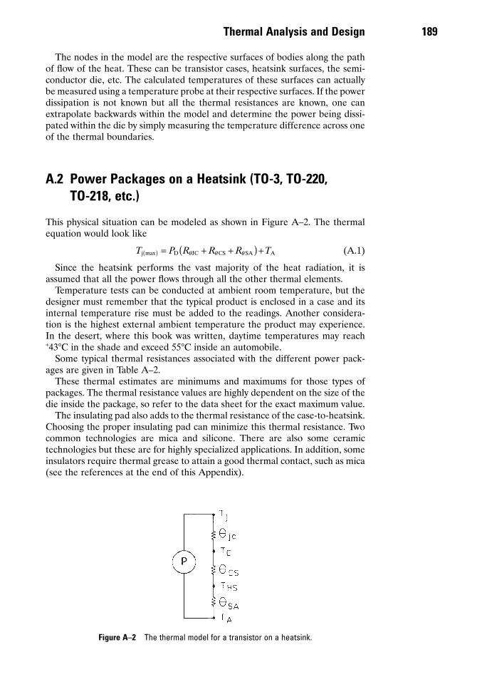
Thermal Analysis and Design 189
The nodes in the model are the respective surfaces of bodies along the pathof flow of the heat. These can be transistor cases, heatsink surfaces, the semi-conductor die, etc. The calculated temperatures of these surfaces can actuallybe measured using a temperature probe at their respective surfaces. If the powerdissipation is not known but all the thermal resistances are known, one canextrapolate backwards within the model and determine the power being dissi-pated within the die by simply measuring the temperature difference across oneof the thermal boundaries.
A.2 Power Packages on a Heatsink (TO-3, TO-220, TO-218, etc.)
This physical situation can be modeled as shown in Figure A–2. The thermalequation would look like
(A.1)
Since the heatsink performs the vast majority of the heat radiation, it isassumed that all the power flows through all the other thermal elements.
Temperature tests can be conducted at ambient room temperature, but thedesigner must remember that the typical product is enclosed in a case and itsinternal temperature rise must be added to the readings. Another considera-tion is the highest external ambient temperature the product may experience.In the desert, where this book was written, daytime temperatures may reach+43°C in the shade and exceed 55°C inside an automobile.
Some typical thermal resistances associated with the different power pack-ages are given in Table A–2.
These thermal estimates are minimums and maximums for those types ofpackages. The thermal resistance values are highly dependent on the size of thedie inside the package, so refer to the data sheet for the exact maximum value.
The insulating pad also adds to the thermal resistance of the case-to-heatsink.Choosing the proper insulating pad can minimize this thermal resistance. Twocommon technologies are mica and silicone. There are also some ceramic technologies but these are for highly specialized applications. In addition, someinsulators require thermal grease to attain a good thermal contact, such as mica(see the references at the end of this Appendix).
T P R R R Tj D JC CS SA Amax( ) = + +( ) +q q q
Figure A–2 The thermal model for a transistor on a heatsink.

A.3 Power Packages Not on a Heatsink (Free Standing)
Power packages not mounted on a suitable heatsink can expect to dissipate lessthan five percent of the maximum specified power capability of the package. So100W devices will only dissipate 1 to 2W when they are free standing. This alsoincludes using the PC board copper plating as a heatsink. Thus, great discretionshould be used when cost is the most important issue.
The thermal model for the case in Figure A–3 is shown in Figure A–4. Thethermal equation becomes
(A.2)
As one can see by the typical values of the junction-to-air thermal resistance, itdoesn’t require much power to result in very high junction temperatures. If thedesigner can possible mount the power package on any metal surface to increasethe radiating surface area, it will only improve the junction temperature.
T P R Tj D JA Amax( ) = ◊ +q
190 Thermal Analysis and Design
Table A-2 Thermal Resistances of Common Thru-hole Power PackagesPackage Minimum Maximum Minimum Maximum
TO-3 * 30.0 0.7 1.56TO-3P * 30.0 0.67 1.00T0–218 * 30.0 0.7 1.00TO-218FP * 30.0 2.0 3.20TO-220 * 62.5 1.25 4.10TO-225 * 62.5 3.12 10.0TO-247 * 30.0 0.67 1.00DPACK 71.0 100.0 6.25 8.33
Figure A–3 A free-standing power package.
Figure A–4 Thermal model of a free-standing power package.

Thermal Analysis and Design 191
A.4 Radial-leaded Diodes
The diodes within the power supply typically dissipate a large amount of power.These are the input rectifiers and the output rectifiers. In a bipolar centeredswitching power supply, the output rectifiers dissipate as much power as thebipolar power switches, so their contribution to the heat within the system issignificant. The physical situation is shown in Figure A–5.
As one can see, the thermal parameters define a physically different situa-tion. For a radial-leaded diode, the heat can only be conducted from the die,via the leads. The thermal resistance would then change as a function of lead-length and is published this way in data sheets. The thermal expression (seeFigure A–6a) is
(A.3)
This is for the typical PC board-mounted application where only the PC boardtraces are used to conduct the heat away from the diode. The typical value rangeof the lead-to-air thermal resistance is between 30 to 40°C/W and is a variablewhich is dependent on the lead length.
T P R Tj D LA Amax( ) = ◊ +q
Figure A–5 Physical diagram of a mounted diode.
Figure A–6 The thermal model for an axial-leaded diode.

There are some heatsinks for radially-leaded diodes that solder to one of theleads. These are also available from the transistor heatsink manufacturers. Inthis situation the thermal equation (see Figure A–6b) becomes
(A.4)
These heatsinks will help a marginal heat situation. The alternative is to usea rectifier in a power transistor package such as a TO-220, TO-218, etc., andplace it on a heatsink or to investigate a different technology of diode thatexhibits a lower forward voltage drop such as a Schottky.
A.5 Surface Mount Parts
The use of surface mount parts is widespread. Surface mount parts can rid them-selves of heat only through their leads which are soldered to a printed circuitboard. The thickness and surface area of the copper island become the heatsinksystem. The thermal resistances in surface mount devices are much higher,therefore their designs have much less margin and room for error. Table A–3has nominal values for thermal resistances of common surface mount packages.Please refer to the individual part data sheet for the exact value.
It is very important to select the package is appropriate for the function beingperformed. For switching signals, which are signal currents of less than 50 mA,the SOT23, SOD123, and other simple packages with gull-wing, J-leaded, andsolder bump leaded packages are very compact and economical. For currentsof 100mA through amperes, the package must have a tab or multiple leads con-nected directly to the die. This is typically the drain, collector, or cathode. Thecommon packages are the SOT223, DPAK, SMB, and SMC. These tabs offer avery low resistance channel to remove the heat from the die and get it onto thePC board for dissipation.
In surface mount printed circuit board applications, more than one issueusually must be considered. Heatsinking must be considered, along with signaland EMI/RFI considerations. The trace that must dissipate the greatest heatwithin a switching power supply is also the node that has the largest dv/dts whichcouple very easily to the surrounding traces.
T P R R Tj D JL SA Amax( ) = +( ) +q q
192 Thermal Analysis and Design
Table A-3 Typical Surface Mount Package Thermal ResistancesPackage J-A1 J-C2
SOD123 340 150SOT23 556 75SOT223 159 7.5SO-8 63 21SMB 13SMC 11DPAK 80 6D2PAK 50 2
1 Theremal resistance for a reference pad size.2 Thermal resistance for a very large pad size.

Thermal Analysis and Design 193
Laying out heatsinking systems for surface mount packaging technologysystems is still an uncertain process. Semiconductor manufacturers still do notoffer adequate information for each power package to feel confident about theadequacy of the heatsinking design. The graph in Figure A–7 is a normalizedplot based upon a SOT223 package. The curve is 2oz copper on the top of thePCB only. The curve, such as contained in Figure A–7, are needed to properlysize the PC board heatsink island.
A.6 Examples of Some Thermal Applications
These examples will show the reader a typical application of thermal analysisbut with common application variations. These variations are useful in definingthermal boundaries within a design.
A.6.1 Determine the Smallest Heatsink (or Maximum Allowed ThermalResistance) for the Application
This approach is useful for determining the smallest possible heatsink that anapplication can use before the thermal limit of a power device is exceeded. Thisis an example of a consumer market approach to designing a heatsink system.
SpecificationThe device is an FDP6670 (Fairchild MOSFET) in a switching power supply.Convection cooling.
1.0
0.9
0.8
0.7
0.6
0.1 0.2 0.3 0.4
Specified Theta J-A
Heatsink Pad Area (sq-in)
Nor
mal
ized
The
rmal
Res
ista
nce
J-A
.
Figure A–7 Example of the effect of increasing pad area versus theta JA.

PD = 10 watts
The thermal model is shown in Figure A–8.Rearranging Equation A.1 and solving for the thermal resistance of the
heatsink,
(A.5)
qCS is assumed at 1.0°C/W. Being conservative by not requiring the junctionat its maximum temperature makes the maximum allowable junction tempera-ture 150°C. The result is
The PC board-mounted heatsink choices are: Thermalloy part numbers7021B through 7025B for low-cost sheet-metal type heatsinks.
A.6.2 Determine the Maximum Power That Can Be Dissipated by a Three-terminal Regulator at the Maximum Specified Ambient Temperaturewithout a Heatsink
A 3-terminal regulator’s overcurrent protection is totally dependent upon theheatsinking system. When the die reaches approximately 165°C, the regulatorshuts down. This example demonstrates the nonheatsink capabilities of amA7805.
SpecificationThe desired 3-terminal regulator is a mA7805KC (TO220) (Texas Instruments).
TJ(max) 150°CTA(max) +50°CVin(max) 10.0VDCIout(max) 200mA
The power dissipated by the regulator is qJA C W= ∞22
qSA C Wmax .( ) = ∞7 0
q q qSA J A D JC CSmax( ) < -( ) - -T T P
TJ Cmax( ) = ∞175 qSA C W Thermalloy P N 53-77-5= ∞ ( )0 53.
qJC C W= ∞2 0.
TA Cmax( ) = + ∞50
194 Thermal Analysis and Design
Figure A–8 Thermal model for design example A.6.1.

Thermal Analysis and Design 195
(A.6)
or
PD = 1.0W
The thermal model is that of Figure A–4, and the thermal equation is Equa-tion A.2 rearranged to
(A.7)
So the mA7805KC will operate within its maximum junction temperature ratingsfor this application.
A.6.3 Determine the Junction Temperature of a Rectifier with a KnownLead Temperature
This is useful in verifying whether a diode’s junction temperature is within itssafe operating temperature.
SpecificationThis is a Zener diode, shunt regulator application. The diode is a 1N5240B (10V(nom), +/- 5%).
IZ(max) 50mATA(max) +50°CTL +46°C (measured at TA = +25°C)Lead length 3/8 inch (1.0cm) each (175°C/W)
The worst-case power dissipation is
This situation would fit the thermal model as seen in Figure A–7b. It doesnot matter in this case not all the elements of the model are known since all theelements above the lead temperature node are known for this first step. Thethermal expression for the temperature rise above the measured lead tem-perature is
(A.8)
or
The junction temperature at the specified maximum local ambient tempera-ture is
(A.9)
The maximum junction temperature specified in the data sheet is +200°C, sothe junction will be operating safely.
TJ Cmax( ) = ∞142 T T TJ J rise Amax max( ) ( ) ( )= +
Tj W C W C rise= ( ) ∞( ) = ∞0 525 175 92.
T PJ rise D JL( ) = ◊q
PD V mA mW or W= ( )( ) =1 05 10 50 525 0 525. .
TA Cmax( ) = ∞128
TA C W C Wmax . deg( ) = ∞ - ( )( )150 1 0 22 T T PA J MAX D JAmax( ) ( )= - ◊q
P V V ID in out out= -( ) ◊( ) ( )max max

Appendix B. Feedback LoopCompensation
196
The heart of every linear and switching power supply is a negative feedback loopwhich maintains a constant value for the output voltage(s). To accomplish this,an error amplifier is used, which attempts to minimize the error between theoutput voltage and an ideal reference voltage. If the world were well behaved,a very high-gain inverting amplifier would be used and this job would be simple.The reality is that loads change, and the input voltage suddenly goes up or down. The error amplifier must respond to these changes quickly and withoutoscillating. This is complicated because the response in the power portion ofthe power supply is relatively “lethargic.” If the error amplifier takes too longto respond to these changes, the supply behaves sluggishly. If the response isspeeded up, the supply reaches a point where it may oscillate. So the problembecomes one of how fast and to what degree the response of the error ampli-fier should tailored to the power circuits.
Do not feel alone in your apprehensiveness about your knowledge in this area.There are few engineers that understand feedback loop compensation, becauseits been “cluttered” with too much fundamental mathematics that is not easilytransferable to the actual circuit design. My approach is an easy step-by-stepmethod which has always worked in my designs and can be completed in lessthan 20 minutes.
B.1 The Bode Response of Common CircuitsEncountered in Switching Power Supplies
The Bode plot is a good method for working with feedback systems over a rangeof frequencies. It does employ logarithms, so a scientific calculator will beneeded. The purpose of this section is not to teach the reader everything he orshe needs to know about Bode plots, but instead should give a reasonable under-standing of the behavior of the actual circuit elements and what their influencesare on the responsiveness of the supply.
The Bode plot is actually composed of two graphs: a gain vs. frequency graphand a phase vs. frequency graph. It is a representation of the relative gain andphase shift of the output voltage signal referenced to the input voltage signalcontributed by any 2-port circuit stage. When more than one circuit stage is cas-caded together, their respective Bode responses can simply be added togetherto yield a combined Bode response.
Simple combinations of components produce responses which are called polesand zeros. A single pole (Figure B–1) produces a flat gain response from dc to

Feedback Loop Compensation 197
its corner frequency. It then produces a -20dB/decade gain slope above its cornerfrequency. The corner frequency is the frequency at which the impedances ofthe two components equal one another. At least one of the components is reac-tive, which means the value of its impedance varies with the frequency. Theimpedance value of an inductor (ZL = j2p fL) increases with frequency and itsbranch current always leads the branch voltage by 90 degrees. The impedancevalue of a capacitor (ZC = 1/j2p fC) starts at infinity at dc and drops with fre-quency, and its current always lags the voltage by 90 degrees. In Figure B–1, asimple low-pass filter, the capacitor starts with an impedance at dc of infinity;then when the capacitor impedance equals the resistor value, an ac voltagedivider is formed where the output amplitude is one-half the input amplitude.This is called the 6dB point. The output phase as compared to the input voltageis -45 degrees, which means that it is lagging the input signal. Eventually, itsphase would reach 90 degrees as the impedance of the capacitor becomes mag-nitudes larger than that of the resistor. The rule-of-thumb for phase is that allphase influences from a pole or zero occur within a +/-1 decade about its cornerfrequency. A zero (Figure B–2) is just the opposite from a pole. It has a flatgain response from dc to its corner frequency, then proceeds at a +20dB/decadegain response and a maximum phase lead of +90 degrees.
There are circuits within switching power supplies that exhibit double poleresponses. This is where both elements in the stage are reactive, such as the L-C filter on the output stage of a forward-mode converter. This is best seen inFigure B–3. Here the response is flat from dc to its resonance frequency andthen exhibits a -40dB/decade gain response and a -180 degree lagging phaseresponse at high frequencies. Lagging phase corresponds directly to a time delaythrough the forward-mode switching power supply output filter.
In switching power supplies, operational amplifiers (op amps) are used toalter the Bode functions (refer to Figure B–4). First, the op amp contributes anadditional -180degrees of lag (inverting amp) and any pole or zero adds or sub-tracts gain and phase from this -180 degree starting point. The generalized erroramp is seen in Figure B–4. With op amps, a corner frequency of a simple poleor zero is defined as:
Figure B–1 A single-pole RC low-pass filter.

Zin = Zfb (B.1)
Some implementations of these error amp circuits are shown in Figures B–5through B–7. Some useful mathematical tools when working with Bode plotsare given below.
198 Feedback Loop Compensation
Figure B–2 A simple zero differentiator or high-pass filter.
Figure B–3 A two-pole filter: choke input filter.
Figure B–4 A generalized error amplifier.

Feedback Loop Compensation 199
1. To find values of gain and phase at a different frequencies along a -20dB/decade gain slope and its associated phase curve:
(B.2)
(B.3)
2. To find values of gain and phase at different frequencies along a -40dB/decade gain slope and its associated phase curve:
f f ff
f2 1
1 2
1
-( ) = ÊËÁ
ˆ¯
-tan
DG f ff
f2 1
2
1
20-( ) = ÊËÁ
ˆ¯log
Figure B–5 An active single-pole filter.
Figure B–6 An active single-pole filter with flat high- and low-frequency responses.

(B.4)
(B.5)
These tools and circuits form the basis of the design approach within the feed-back loop compensation circuits in power supplies.
f f ff
f2 1
1 2
1
2-( ) = ÊËÁ
ˆ¯
-tan
DG f ff
f2 1
2
1
40-( ) = ÊËÁ
ˆ¯log
200 Feedback Loop Compensation
Figure B–7 An active high-pass filter (single zero) with flat high- and low-frequencyresponses.
Figure B–8 Illustrating how the mathematical tools are used.

Feedback Loop Compensation 201
B.2 Defining the Open Loop Response of the SwitchingPower Supply—The Control-to-OutputCharacteristics
Before the designer can begin to develop a stable negative feedback circuit, thebehavior of the system that is to be controlled must be defined. To do this, thedesigner should have a general understanding of what each of the major sec-tions of the switching power supply contributes to the entire open-loop Boderesponse of the switching power supply. Fortunately, the commonly employedtopologies, as described in this book, have previously been defined and fall into two major responses. The choice of which response to use is easily madefrom the design path that has been previously chosen by you. The response types are
1. Voltage-mode controlled forward-mode converters.2. Voltage-mode controlled flyback-mode converters, and current-mode con-
trolled forward- and flyback-mode converters.
The matter of whether or not the topology is transformer-isolated has aninfluence only on the dc characteristics of the model. The flyback-mode con-verters mentioned above are operating in the discontinuous mode of operationonly.
The control-to-output characteristic is simply the behavior of the power supplywhen the error amplifier is removed from the system. The point where the errorvoltage enters the PWM-to-pulsewidth converter is viewed as the input port ofthe system. The point where the output voltage feedback enters the error ampli-fier’s negative input is the output port of the system. This can be seen in FigureB–9. When the “input” is swept with a sweep generator, the resulting Bode plotis the control-to-output characteristic. This is the plot which is most meaning-ful for the purposes of stabilization. An approximate control-to-output plot mayalso be done by the following procedure with very satisfactory results.
B.2.1 The Voltage-mode Controlled Forward-mode ConverterThe common topologies which are encompassed under this category are: thebuck, half-forward, push-pull, half and full bridge, with only the traditionalvoltage-mode control method. Its representative circuit diagram is given in
Figure B–9 The meaning of the control-to-output characteristic.

Figure B–10. Figure B–10 shows the presence of a transformer. For the buckconverter, the designer can assume that the turns ratio is 1:1.
The first step is to determine the gain of the system at dc. This is the start-ing point for developing the gain plot. The dc gain is found by
(B.6)
where DC is the maximum duty cycle (~95 percent).DVe is the peak-to-peak output voltage of the error amplifier.
To convert the dc gain into decibels,
(B.7)
GDC is then the starting point of the gain Bode plot at dc.The first major pole is contributed by the output L-C filter. It represents a
second order pole which exhibits a “Q” phenomenon, which is typically ignored,and a -40dB/decade rolloff above its corner frequency. The phase plot willquickly begin to lag starting at a frequency of 1/10th the corner frequency, andwill reach the full 180 degrees of lag at 10 times the corner frequency. The loca-tion of this double pole is found from
(B.8)
where Lo and Co are the values of the inductor and capacitor in the output L-C filter (in henries and farads). If there are multiple outputs on the switching
fL C
p
o o
=1
2p
G ADC DCLog= ( )20
AV
V
N
ND
V
V
N
NDC
out
in pri
in
e pri
C= = ◊ = ◊sec sec
D
202 Feedback Loop Compensation
Figure B–10 The control-to-output model for a voltage-mode controlled forward converter.

Feedback Loop Compensation 203
power supply, then use the filter values from the highest power output that issensed.
The next item is the zero exhibited by the series combination of the ESR ofthe output filter capacitance and the actual value of the output filter capacitoritself. Its corner frequency is found from
(B.9)
This causes the control-to-output characteristic to add gain and phase above thelocation of this zero. This can be a problem with respect to the stability of thesupply. Unfortunately, many capacitor manufacturers do not present the valueof the ESR for their capacitors. Typically, the zero caused by the output filtercapacitor falls in the following range:
Aluminum electrolytic 1–5kHzTantalum 10–25kHz
As one can see, the choice of the type of output filter capacitor can influencethe control-to-output characteristic, sometimes detrimentally.
The resulting control-to-output Bode plots for the voltage-mode controlledforward converter are given in Figure B–11.
B.2.2 Voltage-mode Controlled Flyback Converter and Current-modeControlled Forward-mode Converter Control-to-OutputCharacteristics
The operation of a discontinuous-mode, flyback converter is quite differentfrom that of a forward-mode converter, and likewise their control-to-outputcharacteristics are very different. The topologies that fall into this category ofcontrol-to-output characteristics are the boost, buck/boost, and the flyback. Theforward and flyback-mode converters operating under current-mode controlalso fall into this category. Only their dc value is determined differently. Theirrepresentative circuit diagram is given in Figure B–12.
The dc gain exhibited by the power section of the switching power supply ofa current- or voltage controlled flyback converter is approximately
(B.10)
DVe in this case can be the peak-to-peak voltage of the oscillator ramp if themethod of control is voltage-mode, or the maximum peak voltage representingthe primary current within the current-mode method of control. The gain canbe converted into decibels, which is shown in Equation B.7.
The current-mode controlled forward-mode converter exhibits the same dc gain as the voltage-mode controlled forward converter, as shown in Equation B.6.
The output filter pole in both voltage-mode controlled flyback converter andthe current-mode controlled forward and flyback is highly dependent on theequivalent resistance of the load. This means that when the load currentincreases or decreases, the location of the output filter pole moves. The filterpole can be found from
(B.11)
where RL is Vout/Iout.
fR C
p
L o
=1
2p
AV V
V V
N
NDC
in out
in e pri
=-( )◊
◊2
Dsec
fR C
ESR
ESR o
=◊
1
2p
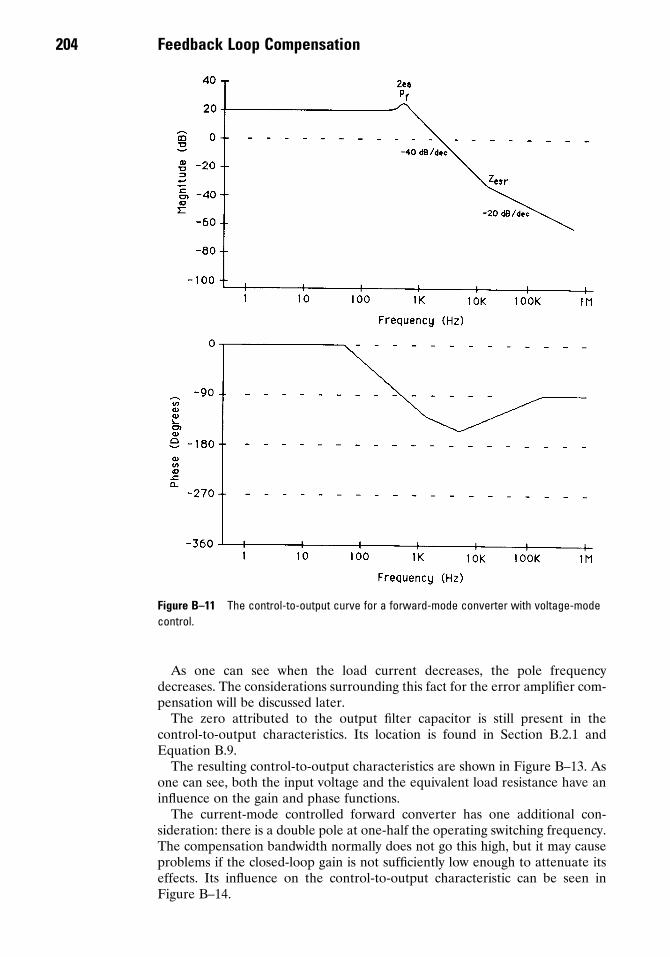
As one can see when the load current decreases, the pole frequencydecreases. The considerations surrounding this fact for the error amplifier com-pensation will be discussed later.
The zero attributed to the output filter capacitor is still present in the control-to-output characteristics. Its location is found in Section B.2.1 andEquation B.9.
The resulting control-to-output characteristics are shown in Figure B–13. Asone can see, both the input voltage and the equivalent load resistance have aninfluence on the gain and phase functions.
The current-mode controlled forward converter has one additional con-sideration: there is a double pole at one-half the operating switching frequency. The compensation bandwidth normally does not go this high, but it may causeproblems if the closed-loop gain is not sufficiently low enough to attenuate itseffects. Its influence on the control-to-output characteristic can be seen inFigure B–14.
204 Feedback Loop Compensation
Figure B–11 The control-to-output curve for a forward-mode converter with voltage-modecontrol.

Feedback Loop Compensation 205
B.3 The Stability Criteria Applied to Switching PowerSupplies
Before starting the design for the compensation of the error amplifier, it is desirable to know what constitutes a stable closed-loop system. The rule is elementary:
The closed loop phase shall never exceed -330 degrees of lag whenever thegain of the closed-loop system is greater than 1 (or 0dB).
Actually, a total closed-loop phase lag limit of 315 degrees is commonly usedby designers; any closer to 360 degrees would constitute a metastable system.This could result in the power supply breaking out into periods of oscillationwhen large loads or line transients are experienced.
Figure B–15 shows some of the terms encountered in stability analysis.
1. Phase margin. This is the value of the phase of a closed-loop system at thegain cross-over frequency (G(s) = 0dB).
2. Gain margin. This is the value of the gain when the phase crosses over -360 degrees.
3. Excess phase. This is the point of closest approach of the phase character-istic to -360 degrees anytime the gain is greater than 1 (0dB).
The excess phase is the most important consideration of the three, since thegain cross-over frequency is usually much higher than the point of maximumphase lag caused by a filter pole.
Figure B–12 The control-to-output model for a voltage-mode controlled flyback converter.
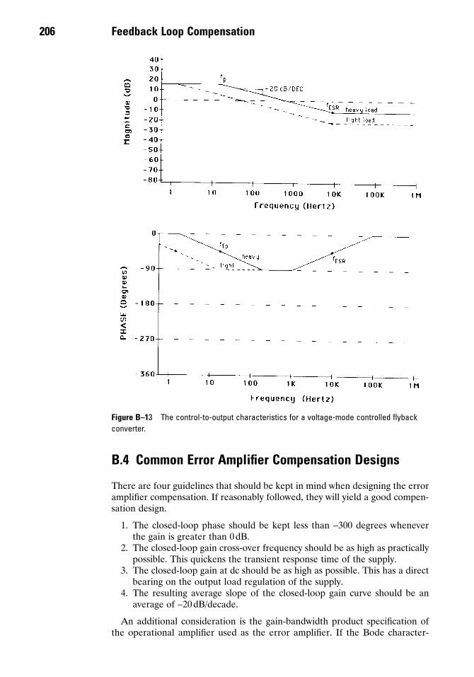
B.4 Common Error Amplifier Compensation Designs
There are four guidelines that should be kept in mind when designing the erroramplifier compensation. If reasonably followed, they will yield a good compen-sation design.
1. The closed-loop phase should be kept less than -300 degrees wheneverthe gain is greater than 0dB.
2. The closed-loop gain cross-over frequency should be as high as practicallypossible. This quickens the transient response time of the supply.
3. The closed-loop gain at dc should be as high as possible. This has a directbearing on the output load regulation of the supply.
4. The resulting average slope of the closed-loop gain curve should be anaverage of -20dB/decade.
An additional consideration is the gain-bandwidth product specification ofthe operational amplifier used as the error amplifier. If the Bode character-
206 Feedback Loop Compensation
Figure B–13 The control-to-output characteristics for a voltage-mode controlled flybackconverter.

Feedback Loop Compensation 207
istics of the op amp are too low in frequency, the desired compensation schememay not work completely.
The compensation schemes shown in this book are the most commonmethods. Several of these will work in each applications, but only one for eachis considered the optimum method insofar as the dc gain and closed-loop band-width aspects are concerned. Tables B–1 and B–2 will help match a possiblecompensation method with your application.
B.4.1 Single-pole CompensationThis type of compensation is used for those converter topologies that exhibitminimal phase shift prior to the anticipated closed-loop gain cross-over point.This topology would be that of the forward-mode converters using voltage-modecontrol. This compensation method, though requiring the minimum amount ofparts and excellent load regulation, yields a very poor closed-loop bandwidththat produces a sluggish transient response time.
Figure B–14 The control-to-output characteristics for a current-mode controlled forwardconverter.

The schematic and Bode plot for the single-pole method of compensation aregiven in Figure B–16. At dc it exhibits the full open-loop gain of the op amp,and its gain drops at -20dB/decade from dc. It also has a constant -270 degreephase shift. Any phase shift contributed by the control-to-output characteristic
208 Feedback Loop Compensation
Figure B–15 The definition of stability terms.

Feedback Loop Compensation 209
cannot then add more than the desired excess phase (-315 to -330 degrees) oran additional 30 to 45 degrees.
The first step in determining the component values for this compensationmethod is to determine the inherent dc gain of the power stages. The calcula-tion should be performed with the maximum value of the input voltage, sincethis is where the system will have its widest exhibited bandwidth. This is doneusing Equation B.12.
(B.12)
Refer to Section B.2.1 for any additional help. Do not yet convert this value to dB.
Next find the closed-loop gain cross-over frequency by deciding how much phase margin you desire in your system. A good value is 45 degrees. Ignoring any effect of the Q of the L-C filter, the gain cross-over point is found from
AV
V
N
NDC
in
e pri
= ◊D
sec
Figure B–16 The single-pole method of compensation.

(B.13)
Next find the cross-over frequency of the error amplifier from
(B.14)
Then find the value of the feedback capacitor C. The designer knows the valueof the input resistor (R). It is the upper resistor in the voltage divider respon-sible for the voltage feedback to the error amplifier. One then performs Equation B.15.
(B.15)
This compensation method, although easy to design, exhibits very sluggishtransient load response. This is because the gain cross-over point is always muchlower than that of the output filter pole. This usually results in loop bandwidthsof 50 to 500Hz. This may cause a problem to the load circuitry by having thesupply voltages exhibit momentary excursions outside their operating specifica-tions. Figure B–17 shows an implementation of this compensation method. As one may be able to see, a high Q characteristic of the L-C filter can cause
CA
Rf= DC
xe2p
f f Axe xo
xo= ◊ -( )10 20
f fxo fp pmTan= ( )f 2
210 Feedback Loop Compensation
Figure B–17 Single-pole compensation used with a voltage-mode controlled forwardregulator.
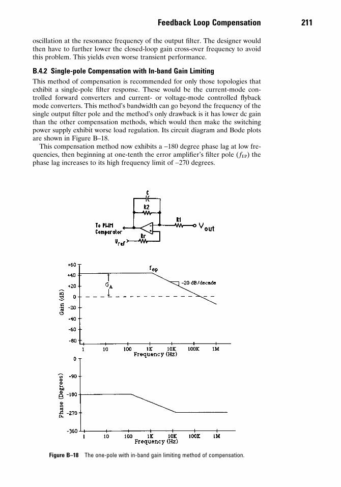
Feedback Loop Compensation 211
oscillation at the resonance frequency of the output filter. The designer wouldthen have to further lower the closed-loop gain cross-over frequency to avoidthis problem. This yields even worse transient performance.
B.4.2 Single-pole Compensation with In-band Gain LimitingThis method of compensation is recommended for only those topologies thatexhibit a single-pole filter response. These would be the current-mode con-trolled forward converters and current- or voltage-mode controlled flybackmode converters. This method’s bandwidth can go beyond the frequency of thesingle output filter pole and the method’s only drawback is it has lower dc gainthan the other compensation methods, which would then make the switchingpower supply exhibit worse load regulation. Its circuit diagram and Bode plotsare shown in Figure B–18.
This compensation method now exhibits a -180 degree phase lag at low fre-quencies, then beginning at one-tenth the error amplifier’s filter pole ( fEP) thephase lag increases to its high frequency limit of -270 degrees.
Figure B–18 The one-pole with in-band gain limiting method of compensation.

To begin the design process, one of course needs the inherent maximum dcgain exhibited by the power circuit’s control-to-output characteristic (ADC). Theworst-case condition is considered at the highest input voltage. The closed-loopgain cross-over frequency is limited to one-fifth the switching frequency. This isbecause if the cross-over frequency were higher, too much of the switching fre-quency would be amplified by the error amplifier which would bbe detrimental.So the closed-loop gain cross-over frequency is
fxo < 0.2 fsw (B.16)
where fsw is the switching frequency of the switching power supply.The location of the error amplifier’s pole is used to counteract the effects of
the output filter capacitor’s zero caused by the ESR. The error amplifier’s poleshould be located by
(B.17)
Next, one must determine the amount of gain needed by the error amplifierto bring the control-to-output function up to 0 dB at the closed-loop cross-overfrequency:
(B.18)
To find the amount of gain needed below the error amplifier pole;
(B.19)
To find the value of the feedback capacitor, one evaluates the following:
(B.20)
(B.21)
To find the feedback resistor value,
(B.22)
R2 = AA · R1 (B.23)
This completes the design of the single-pole with in-band gain limitingmethod of compensation. Its closed-loop Bode plot can be seen in Figure B–19.If you attempt this method, there is one drawback. Due to the high-gain andwide bandwidth nature of this method, it is very easy to encounter the maximumgain-bandwidth characteristics of the op amp itself. That is, the op amp may nothave enough gain at the frequencies required. There are two alternatives: lowerthe crossover point, or use an external op amp with a higher GBW specification.
B.4.3 Pole-Zero CompensationThis compensation method is intended for those topologies that exhibit a singlefilter pole response. That would include: the voltage-mode controlled, discon-tinuous, flyback converter, and the current-mode controlled forward and flybackconverters. It possesses a high dc gain, and a phase lead characteristic. Thismethod gives the designer the opportunity to tailor the compensation to thepower supply. Its circuit and Bode response can be seen in Figure B–20.
A GGA a
A absolute gain of= ( )( )10 20
CR A f
=1
2 1p xo ep
A GGxo xo
xo absolute gain of= ( )( )10 20
G Gf
fA xo
xo
ep
= + ÊËÁ
ˆ¯
20 log
Gf
fGxo
xo
fp
DC in dB= ÊËÁ
ˆ¯
- ( )20log
f fEP Z ESR lowest frequencyª ( )( )
212 Feedback Loop Compensation

Feedback Loop Compensation 213
This compensation method has a pole at dc that provides the open-loop opamp gain for good output regulation. A zero is introduced at or below thesupply’s lowest manifestation of the output filter pole in order to compensatefor the phase lag by that pole. The phase lag of the error amplifier actuallydecreases between the error amplifier’s zero and pole. Its theoretical limit is -180 degrees (or +90 degree “phase bump”). This phase bump should be placedwhere the greatest phase lag from the output filter pole will exist. In that way,good control over the excess phase of the system can be maintained. The lastpole is put into the compensation to roll off the gain at high frequencies and tocounteract the capacitor’s zero caused by the ESR. Its closed-loop Bode plotcan be seen in Figure B–21.
To begin the design, the inherent dc gain of the control-to-output character-istic should be found. For voltage and current-mode controlled flyback con-verters, refer to Equation B.10. For current controlled forward-converters referto Equation B.6. These should be calculated at the highest input voltage sincethat will yield the highest dc gain (worst case).
Next determine the maximum closed-loop gain cross-over frequency. Lessthan one-fifth of the switching power supply’s operating frequency is a goodrule.
fxo £ .2 · fSW (B.24)
Figure B–19 An example of single-pole with in-band gain limiting compensation used witha voltage/current-mode controlled flyback converter.

Determine how much gain is required to elevate the control to output gain curveto 0dB at the gain cross-over frequency.
(B.25)
The next task is to determine the placement of the compensating zero andpole within the error amplifier. The zero is placed at the lowest frequency manifestation of the filter pole. Since for the voltage-mode controlled flybackconverter, and the current-mode controlled flyback and forward converters, this pole’s frequency changes in response to the equivalent load resistance. The lightest expected load results in the lowest output filter pole frequency. The error amplifier’s high frequency compensating pole is placed at the lowestanticipated zero frequency in the control-to-output curve cause by the ESR ofthe capacitor. In short:
Gf
fGxo
xo
fp
DC= ÊËÁ
ˆ¯
-20 log
214 Feedback Loop Compensation
Figure B–20 The pole-zero compensation method.

Feedback Loop Compensation 215
(B.26)
and
(B.27)
Now the component values can be calculated. The value of the input resistor(R1) is known since it is the upper resistor in the feedback voltage divider. Thevalue of the feedback components are found as follows:
(B.28)
R2 = Axo · R1 (B.29)
where Axo is the absolute value for the gain needed at the cross-over frequency(non dB).
(B.30)
The amount of phase boost exhibited by the error amplifier is
Cf R
21
2 2=
p ez
Cf A R
11
2 1=
◊ ◊p xo xo
f f fep ep Z ESR-min: = ( )
f f fez ez fp light load: = ( )
Figure B–21 An example of pole-zero compensation used with a voltage/current-modecontrolled flyback converter.

(B.31)
The phase boost is proportional to the separation of the zero-pole pair in theerror amplifier, but that is of secondary nature since the error amplifier’s poleand zero were placed to compensate the worst case zero and pole in the control-to-output characteristics. The actual location of the zero caused by the ESR,which amounts to the choice of a vendor and part number, will affect the amountof excess phase the supply will exhibit. So the designer may have to relocate thecompensating pole if there is any possibility that the excess phase will fall to lessthat 30 degrees (-330 degree lag).
B.4.4 2-Pole–2-Zero CompensationThis compensation is intended for voltage-mode controlled forward converterswhich exhibit a second order output filter pole characteristic. This would alsoinclude a quasi-resonant forward-mode converter that uses variable frequency,voltage-mode control. The L-C filter has a severe 180 degree phase lag and a -40dB/decade gain rolloff. To get any sort of wide bandwidth from the supplyat all, this type of compensation must be used.
This method has a pair of zeroes that counteract the gain and especially thephase of the double filter pole (see Figure B–22). This results in a closed-loopslope of -20dB/decade above the filter pole. It also has a high-frequency poleto counteract the capacitor induced zero caused by the ESR. Lastly, it has a veryhigh frequency pole to guarantee that the phase and gain margins at the closed-loop gain and phase cross-over frequencies are well behaved.
The more complicated methods of compensation, such as this, allow thedesigner much more control over the final closed-loop bode response of thesystem. The poles and zeros can be located independently of one another. Oncetheir frequencies are chosen, the corresponding component values can be easilydetermined by the step-by-step procedure below. The zero and pole pairs canbe kept together in pairs, or can be separated. The high-frequency pole pairappear to yield better results if they are separated and placed as below. Thezero pair are usually kept together, but can be separated and placed either sideof the output filter pole’s corner frequency to help minimize the gain effects ofthe “Q” of the L-C filter (refer to Figure B–23).
To begin the design process, the inherent dc gain of the control-to-output gainfunction (Gdc and Adc) is found using equations B.6 and B.7.
Next, the maximum closed-loop gain cross-over frequency (fxo) is determinedand is, once again, no more than one-fifth the minimum switching of the switch-ing power supply:
(B.32)
Determine the amount of gain that is required to bring the control-to-outputgain function up to 0 dB at the gain cross-over frequency. This can be approxi-mated from
(B.33)
Determine the placement of the compensating zeroes (fez1 and fez2). If thezeroes are to be placed at the same frequency, then
Gf
fGxo
xo
fp
DC= ÊËÁ
ˆ¯
-40 log
f fxo sw< ( ).2
fBoost
ep
ez
= ÊËÁ
ˆ¯
- ∞-2 901tanf
f
216 Feedback Loop Compensation

Feedback Loop Compensation 217
(B.34)
If the zeroes are to be placed on either side of the filter poles, then
(B.35)
and
ffp £ fez2 £ 1.2 ffp (B.36)
Next, place the lowest frequency error amplifier pole (fep1) at the lowest anticipated capacitor ESR zero frequency:
(B.37)
The highest frequency compensating pole ( fep2) is slightly higher in frequencythan the gain cross-over frequency:
f fep z ESR1 = ( )
f fez fp1 5=
f f fez ez fp1 2 2= =
Figure B–22 2-Pole–2-zero compensation.

fep2 ≥ 1.5 fxo (B.38)
Now one can determine the component values. One first calculates the gainat the location of the two compensating zeros (A1). (See Figure B–22 for themeanings of the variable.)
(B.39)
Then
(B.40)
R2 = A1 · R1 (B.41)
(B.42)Cf R
31
2 12
=p ez
Cf A R
11
2 1 1=
◊ ◊p xo
A G1 10 1 20= ( )
G Gf
f1 2 20 2
1
= + ÊËÁ
ˆ¯
log ez
ep
218 Feedback Loop Compensation
Figure B–23 An example of 2-pole–2-zero compensation used with a voltage-controlledforward converter.

Feedback Loop Compensation 219
(B.43)
(B.44)
where A1 and A2 are the absolute values of the gain (not dB).The method performed above with the placement of the poles and zeroes will
yield a minimum value for the excess phase of 45 degrees, which is satisfactory.If other pole and zero locations are attempted, then locate the maximum phaselag point of the L-C filter at the geometric mean frequency between fez2 and fep1.This will guarantee the best phase performance. The amount of phase boost ofthe compensation design will be
(B.45)fBoost
ez
= ÊËÁ
ˆ¯
- ∞-4 1801 1
2
tan epf
f
Cf R
21
2 22
=p ep
R
R
A3
2
2=

Appendix C. Power Factor Correction
220
Power factor correction is becoming a very important area in the power world.Adding more generating capacity to the world’s electrical pool is very costly andwould consume additional resources. One method of creating about 30 percentexcess generating capacity is to use the ac power more efficiently through thebroad use of power factor correction. Motors, electronic power supplies, andfluorescent lighting consume about 40 percent of the power in the world andeach of these would benefit from power factor correction. From the mid-1990sto 2002, many of the countries of the world are adopting requirements for powerfactor correction for the new products marketed within their borders. Theadded circuitry will add about 20 to 30 percent to the cost of power supplies,but the near-term energy savings will greatly outweigh the initial costs.
The term “power factor” in the field of power supplies is a slight departurefrom the traditional usage of the term, which applied to reactive ac loads, suchas motors, powered from the ac power line. Here, the current drawn by themotor would be displaced in phase with respect to the voltage. The resultingpower being drawn would have a very large reactive component and little poweris actually used for producing work. Since power meters do not measure phase,the power measured is the scaler voltage times current. Capacitor banks are typically used to bring the phase more towards zero degrees if motors are the primary load.
In switching power supplies, the problem lies in the input rectification andfilter network. The typical input circuit and its associated waveforms are shownin Figure C–1. As one can see, the input rectifiers can only conduct current whenthe ac line voltage exceeds the voltage on the input filter capacitor. This typi-cally occurs within 15 degrees of the crest of the ac voltage waveform. The resultis that current pulses are 5 to 10 times higher than the expected average currentdraw. This also can lead to distortion of the ac voltage waveform and an imbal-ance of the three-phase power lines feeding the circuits. This produces a neutralline current where no current flow is expected. Another drawback is that nocurrent is drawn when the rectifiers are not conducting, thus throwing away asignificant portion of the power system’s energy capability.
Power factor correction circuits are intended to increase the conduction angleof the rectifiers and to make the ac input current waveform sinusoidal and inphase with the voltage waveform. The input waveforms can be seen in FigureC–2. This means that all the power drawn from the power line is real power andnot reactive. The net result is that the peak and RMS current drawn from theline is much lower than that drawn by the capacitive input filter circuit tradi-tionally used.
Active power factor correction circuits can take the form of nontransformerisolated switching power supply topologies, such as buck, boost, and buck/boost.The buck topology in Figure C–3 produces an output dc voltage lower thanfound at its input, whenever the PFC stage is operating (Vin > Vout). In other

Power Factor Correction 221
Figure C–1 The waveforms of a capacitive input filter.
Figure C–2 Power factor corrected input.
Figure C–3 A buck power factor correction circuit.
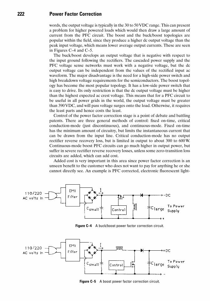
words, the output voltage is typically in the 30 to 50 VDC range. This can presenta problem for higher powered loads which would then draw a large amount ofcurrent from the PFC circuit. The boost and the buck/boost topologies arepopular within the field, since they produce a higher dc output voltage than thepeak input voltage, which means lower average output currents. These are seenin Figures C–4 and C–5.
The buck/boost develops an output voltage that is negative with respect tothe input ground following the rectifiers. The cascaded power supply and thePFC voltage sense networks must work with a negative voltage, but the dcoutput voltage can be independent from the values of the rectified input acwaveform. The major disadvantage is the need for a high-side power switch andhigh breakdown voltage requirements for the semiconductors. The boost topol-ogy has become the most popular topology. It has a low-side power switch thatis easy to drive. Its only restriction is that the dc output voltage must be higherthan the highest expected ac crest voltage. This means that for a PFC circuit tobe useful in all power grids in the world, the output voltage must be greaterthan 390VDC, and will pass voltage surges onto the load. Otherwise, it requiresthe least parts and hence costs the least.
Control of the power factor correction stage is a point of debate and battlingpatents. There are three general methods of control: fixed on-time, critical conduction-mode (just discontinuous), and continuous-mode. Fixed on-timehas the minimum amount of circuitry, but limits the instantaneous current thatcan be drawn from the input line. Critical conduction-mode has no output rectifier reverse recovery loss, but is limited in output to about 300 to 600 W.Continuous-mode boost PFC circuits can go much higher in output power, butsuffer in severe rectifier reverse recovery losses, unless some zero-transition losscircuits are added, which can add cost.
Added cost is very important in this area since power factor correction is anunseen benefit to the customer who does not want to pay for anything he or shecannot directly see. An example is PFC corrected, electronic fluorescent light-
222 Power Factor Correction
Figure C–4 A buck/boost power factor correction circuit.
Figure C–5 A boost power factor correction circuit.

Power Factor Correction 223
ing ballasts at two times the purchase price versus magnetic fluorescent ballasts.Only industrial customers are thoughtful enough to see the vast difference intheir yearly electric bill 12 month later.
The basic PFC controller takes the form as shown in Figure C–6, which wouldinclude the critical and discontinuous-mode circuits and the continuous-modecircuits. There is a multiplier subcircuit inside the control IC which multipliesthe instantaneous value of the input full-wave rectified voltage waveform withthe output of the error amplifier. This produces a current limit signal whichmakes the input current follow the voltage sinusoidal waveshape. The ac inputis filtered by the input EMI filter to produce a 50 to 60 Hz input current wave-form that is free of switching artifacts.
The inductor operating mode is a major consideration in designing a PFCcircuit. The discontinuous-mode of operation is typically used for power levelsless than 300 to 600 W. It has high peak currents that limit its use at the higherinput power levels. For powers greater than 300W, the continuous-mode ofoperation is typically used. This lowers the peak currents seen by the powerswitch and output rectifier and is much easier to filter in the input EMI filtersince there are no rapid transitions in the input switched current waveforms.The only disadvantage is that the diode-related switching losses rise significantlysince the power switch must force the output rectifier to turn off at the begin-ning of each on-time period. The choice of output rectifier (low Trr) becomescritical to the operation of the PFC stage.
How power factor and harmonics are specifiedI strongly recommend that your company engage a third-party EMI testinghouse to test your products. The minimum-level of test equipment required totest for the discussed factors is very expensive and there is a long learning periodinvolved.
The following discussion is primarily based upon EN61000-3-2, which is moreindustrial-based products. EN60555 is the newer version of IEC-555 and coversthe emitted harmonics of household products. Knowing the product class is veryimportant for designing the power factor interface for the ac line. Products thatdraw less than 75W today and 50W in the near future, do not have to complywith the relative limits, only to absolute maximums laid out by the specifica-tions. The limits presented in Table C–1 may change, so please refer to the latest
Figure C–6 A generalized typical power factor control IC.

released version. This is a developing field so be aware of the most recent specifications at the time of your product’s release.
The real power delivered to a load is given by
(C.1)
where
(C.2)
In terms of strictly passive reactive loads, the power factor is the resulting phasebetween the voltage and the current waveforms. In power supplies though, it isthe distortion to the voltage waveform resulting from the time which input rectifiers conduct. Power factor is measured from 0 to 1 where 1 is where all thepower is used by the load (purely resistive). The typical capacitive input filterfound in power supplies has an average power factor of 0.5 to 0.7.
In running the tests, a power analyzer must be used such as the VoltechPM1000, PM1200, or PM3000. Also an audio spectrum analyzer is needed tomeasure the amplitude of the harmonic components of the ac current. The totalinput voltage and currents are given by
(C.3)
and
(C.4)
where the subscript of 1, 2, . . . are the harmonics of 50 or 60 Hz. In power supplies the third harmonic is by far the next largest amplitude and thereforethe largest problem. Harmonics cause problems because, in a pure sense, onlythe fundamental current frequency produces real power. So the reduction ofharmonics produces a better power factor.
A term used in PFC is total harmonic distortion. This is defined as
(C.5)
and it is an indication as to the performance of a PFC circuit.From the power analyzer or the spectrum analyzer, one can measure the
amplitude values needed to verify compliance to the PFC specifications.EN61000-3-2 has the limits shown in Table C–1. Class A and D are shownbecause they are common product categories.
These limits must be measured with a LISN (line impedance stabilizationnetwork) as specified by the regulatory agencies. This makes the input powerline a 50ohm impedance and serves the basis of all of these tests. The test resultsare highly dependent upon the ac line impedance.
Some comments on the design of PFC circuits. First, the EMI filter is an integralpart of any PFC circuit. It filters out the switching harmonics from the inputcurrent waveform. Without an EMI filter, your product will fail the EMI/RFItests which are in addition to the power factor tests. Please refer to AppendixE for information on how to design an EMI filter. Secondly, using a variacduring the measurements will affect the input line impedance and thus affects
T H DI I
I. . .
. . .=
+( ) ( )
( )
1 2RMS RMS
RMS total
I I I IRMS total fund RMS RMS RMS( ) ( ) ( ) ( )= + +2
12
22 . . .
V V V VRMS total fund RMS RMS RMS( ) ( ) ( ) ( )= + +2
12
22 . . .
Power FactorReal Power
Real Power Reactive Power=
+
P V Iin in in Power Factor= ◊ ◊ ( )
224 Power Factor Correction

Power Factor Correction 225
the validity of the data you are trying to measure. Many units will pass testingwithout the use of a LISN, but fail when the LISN is used. The added imped-ance of a LISN distorts the waveforms more than the impedance of the typicalraw ac line in use at that moment. Thirdly, all voltage measurements must bedifferential and use the specified current measuring apparatus.
C.1 A Universal Input, 180W, Active Power FactorCorrection Circuit
This design example demonstrates the design process of a 180W discontinuous-mode boost PFC circuit. It can be scaled to provide output powers up to 200W.The PFC stage is designed to work from every residential ac power systemwithin the world; that is, from 85 to 270VRMS at 50 and 60Hz without the needfor a jumper.
Design specification
AC input voltage range: 85–270VRMSAC line frequencies 50–60HzOutput voltage: 400VDC +/- 10VInput power factor at rated load: >98%Total harmonic distortion (THD) under EN1000-3-2 limits
Predesign considerationsHaving a rating less than a 200 W has many benefits for a power factor correc-tion stage. The major benefit is that it can operate in the discontinuous-mode.Within higher power PFC designs the continuous-mode must be employedwhich presents a significant loss within the circuit due to the reverse recoverytime of the output rectifier. In fixed frequency discontinuous-mode PFC con-trollers, there is still a period when the circuit operates in the continuous-mode(Vin < 50V (approx.)). By employing a critical conduction-mode controller, thedesigner can guarantee that the continuous-mode is never entered.
The first consideration is to determine the peak ac input voltages.
Table C-1 IEC555-2 Harmonic Current LimitsClass A Class D
Harmonic RMS-Amps RMS-Amps
2 1.08 2.303 2.30 —4 0.43 —5 1.44 1.146 0.30 —7 0.77 0.779 0.40 0.40
11 0.33 0.2013 0.21 0.338 < n < 40 0.23 ¥ 8/n
11 < n < 39 0.15 ¥ 15/n 0.15 ¥ 15/n

110V input:
240V input (Britain—worst case):
The output voltage should be higher than the highest anticipated input peakcrest voltage. The output voltage of the PFC stage is now chosen to be 400 VDC.
The maximum value for the peak inductor current will occur at the crestvoltage of the minimum expected ac input voltage. This is
Inductor designIn designing the boost inductor, one would designate the point of reference asthe crest voltage of the minimum expected ac input voltage. For any set of oper-ating conditions with this method of PFC control (i.e., fixed load and ac inputvoltage, the on time pulsewidth remains constant over the entire half-sinusoidwaveform). To determine the on time at the minimum peak ac input voltageone would do the following operations:
R = 3.3
The maximum on time which occurs at this point is
The approximate maximum value of the boost inductor is
The power winding of the inductor (transformer) not only must support themaximum average input current but the output current as well. So, the wiregauge of the winding should be
VP
V
P
V
VA
w max-avout
in RMS
out
out
RMS
mps
effW W
V
( )( )
=( )
+
=( )( )
+ =180
0 9 8 5
180
4002 8
. ..
LT V
P
V
ª( ) ( )
ª( ) ( )( )(
( )ª
( ) ( )
( )
on max in-AC min
out max
RMS
eff
S
WH
2
215 3 1 414 85 0 9
2 180552
2
. . .mm
TR
f Ron max
KHzS
( ) =+( )
=( ) +( )
=1
3 3
50 1 3 315 3
.
.. m
R
V
V V= =
( )( )
( )
out DC
in-AC min RMS
V
2
400
1 414 85.
I P eff V
Vpk max out rated est in min RMS
RMSWA
( ) ( ) ( )= ( )( ) ( )( )= ( )( ) ( )( )=
1 414 21 414 2 180 0 9 856 6
.
. .
.
Vin hi V V( ) = ( ) =1 414 270 381 8. . Vin nom V V( ) = ( ) =1 414 240 339 4. .
Vin hi V V( ) = ( ) =1 414 130 183 8. .
Vin nom V V( ) = ( ) =1 414 110 155 5. .
226 Power Factor Correction

Power Factor Correction 227
The wire gauge to accommodate this average current would then be #17 AWG.I will use three strands of #22 AWG (which adds up to the same wire cross-sectional area), which is more flexible during the winding process and will helpreduce the ac resistance of the winding due to the skin effect. Also, due to thehigh voltages present within the same winding, I will be using quad-thicknessinsulation to reduce the threat of interturn arc-overs.
I am selecting a PQ core style. A major concern is the length of air-gaprequired for various core styles in unipolar applications. The larger air-gaps (>50 mils) cause excessive electromagnetic radiation into the immediate envi-ronment thus making it harder to RFI filter. To reduce the air-gap, one needsto find a ferrite core with the largest core cross-sectional area for a given coresize. The PQ core has this characteristic. Referring to the WaAc vs. power chartsprovided by Magnetics, Inc., the resulting PQ core part number is P-43220-XX.(XX is the gap length in mils).
The approximate air-gap needed in the core is
Let us make the air-gap 50 mils, which is a custom air-gap. Magnetics has no problem with this practice and usually adds only a couple of percent to thecore cost. The inductance factor (AL) for this core with this gap is estimated at160mH/1000T (using a linear extrapolation of AL reduction versus air-gaplength).
The number of turns needed for this inductance is
Checking to see if the core will support this many turns (neglecting the auxiliary winding area):
Designing the auxiliary winding. The auxiliary winding will have the low fre-quency (100 to 120 Hz) variation on its output peak rectified voltage, so the con-troller filter capacitor needs to be large to minimize the droop in the Vcc of thecontroller. The highest flyback-mode rectified voltage will occur at low inputvoltages and will be of the form
This ac waveform is seen in Figure C–7.The MC34262 has a high-side driver clamp of 16VDC, so in order to keep
the high-side driver dissipation to a minimum, the peak voltage of the rectifiedauxiliary voltage should be around 16 V. Determine the turns ratio needed forthis from
v
N V V
Naux
aux out in
pri
ª-( )
A
WW
A
T mm
mmOK=
( )( )=
59 471
4759
2
2
.%
N = =10000 55
16059
. mH
mHturns
lL I
A Bgap
pk
c
H A
cm Gmils
ª◊
ª( )( )
( )( )ª
0 4 10
0 4 552 6 6 10
1 70 2 00066
8
2
8
22
.
. .
. ,
max
p
p m
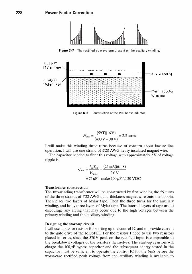
I will make this winding three turns because of concern about low ac line operation. I will use one strand of #28 AWG heavy insulated magnet wire.
The capacitor needed to filter this voltage with approximately 2V of voltageripple is
Transformer constructionThe two-winding transformer will be constructed by first winding the 59 turnsof the three strands of #22 AWG quad-thickness magnet wire onto the bobbin.Then place two layers of Mylar tape. Then the three turns for the auxiliarywinding, and lastly three layers of Mylar tape. The internal layers of tape are todiscourage any arcing that may occur due to the high voltages between theprimary winding and the auxiliary winding.
Designing the start-up circuitI will use a passive resistor for starting up the control IC and to provide currentto the gate drive of the MOSFET. For the resistor I need to use two resistorsplaced in series, since the 370V peak on the rectified input is comparable to the breakdown voltages of the resistors themselves. The start-up resistors willcharge the 100mF bypass capacitor and the subsequent energy stored in thecapacitor must be sufficient to operate the control IC for the 6mS before theworst-case rectified peak voltage from the auxiliary winding is available to
CI T
Vaux
dd off
ripple
mA mS
VF make F VDC
ª =( )( )
=
25 6
2 075 100 20
.@m m
NauxT V
V Vturns=
( )( )-( )
=59 16
400 302 5.
228 Power Factor Correction
Figure C–7 The rectified ac waveform present on the auxiliary winding.
Figure C–8 Construction of the PFC boost inductor.

operate the IC. The start-up voltage threshold hysteresis is 1.75V minimum.Checking whether the bypass capacitor is large enough to start the circuit beforethe turn-off threshold is reached:
I would like to keep the dissipation less than 1W at the high input voltage line.To do this one needs to determine the maximum current that that should passthrough the start-up resistors.
The total resistance is then:
Make the total resistance about 100K or two 47Kohm, 1/2W resistors.
Designing the voltage multiplier input circuitThe minimum specified maximum linear limit of the input to the multiplier(pin3) is 2.5V. This level should be the peak value of the divided rectified inputwaveform at the highest expected ac input voltage at the crest of the sinusoid(370V). If a sense current of 200mA is selected at this point the resistor dividerbecomes
The true sense current is 2.5V/12K = 208mA.The top resistor becomes
Make this two resistors in series each with a value of 910Kohms.The power rating of these resistors are P = (370V)2/1.76 MW or 0.8W. Each
resistor should have 1/2W power rating.
Design of the current sensing circuitThe current sense resistor should be sized in order to reach the 1.1 V currentsense threshold voltage at the low ac input voltage. The value then becomes
A leading edge spike filter of 1K and 470pF will also be added before inputtingthe current signal to pin 4.
Designing the voltage feedback circuitFor the output voltage sense resistor divider, selecting the sense current as 200mA, the lower resistor becomes
RCSV
Aohms= =
1 1
6 60 3
.
..
RtopV V
AMohms=
-=
370 2 5
2081 76
..
m
RbottomV
uAK make it 12 K= =
2 5
20012 5
.. .
RstartV V
mAK=
-= ( )270 16
3 768
.min
Istart
RMS
W
VmA< =
1 0
2703 7
..
VI T
C
V
dropdd off
olts
mA mS
F—OK
= =( )( )
=
25 6
1001 5
m.
Power Factor Correction 229

This makes the true sense current 2.5V/12K = 208mA. The upper resistor is
Make this resistor a 1 Mohm and a 910Kohm resistor in series, each with a 1/2W rating.
The compensation of the voltage error amplifier should be a single-polerolloff with a unity gain frequency of 38 Hz. This is required to reject the fun-damental line frequencies of 50 and 60Hz. The feedback capacitor around thevoltage error amplifier becomes
Designing the input EMI filter sectionI will be using a second order, common-mode filter. The difficulty in consider-ing an input conducted EMI for this power factor correction circuit is its vari-able frequency of operation. The lowest instantaneous frequency of operationoccurs at the crests of the sinusoid voltage waveform. This is where the corerequires the longest time to completely discharge the core. The estimated fre-quency of operation has been 50 kHz, so I will use this as an assumed minimumfrequency.
A good starting point is to assume that I will need 24 dB of attenuation at 50kHz. This makes the corner frequency of the common-mode filter
where Att is the attenuation needed at the switching frequency in negative dB.
Assuming that a damping factor of 0.707 or greater is good and provides a -3dB attenuation at the corner frequency and does not produce noise due toringing. Also assume that the input line impedance is 50ohms since the regu-latory agencies use an LISN test which make the line impedance equal thisvalue. Calculating the values needed in the common-mode inductor and “Y”capacitors:
Real-world values do not allow a capacitor of this large a value. The largestvalue capacitor that will pass the ac leakage current test is 0.05mF. This is 27
Cf
=( )
=( )[ ] ( )
=
1
2
1
2 12 5 9000 18
2 2p p m
mC L kHz H
F.
.
LR
f=
◊
◊=
( )( )( )
=L
C kHzH
z
p pm
50 0 707
12 5900
.
.
fC kHz kHz= ( ) =-Ê
ËÁˆ¯50 10 12 5
24
40 .
f fA
C SW
tt
= ◊ÊËÁ
ˆ¯10 40
Cf R
fb
upper Hz MF or F
= =( )( )
=
1
2
1
2 38 1 820 043 05
p pm m
.. .
RupperV V
uAMohms=
-( )=
400 2 5
2081 91
..
RV
Ibottom
ref
sense
V
uAK Make 12.0K= = =
2 5
20012 5
.. .
230 Power Factor Correction

Power Factor Correction 231
percent of the calculated capacitor value, so the inductor must be increased 360percent in order to maintain the same corner frequency. The inductance thenbecomes 3.24mH and the resultant damping factor is 2.5 which is acceptable.
Coilcraft offers off-the-shelf common-mode filter chokes (transformers) andthe part number closest to this value is E3493. With this filter design I can expecta minimum of -40 dB between the frequencies of 500 kHz and 10MHz. If laterduring the EMI testing stage, I find I need additional filtering, I will add a thirdorder to the filter design by using a differential-mode filter.
The resulting schematic of the power factor correction circuit is given inFigure C–9.
Printed circuit board considerationsThe unit in which this power factor correction circuit resides is going to be mar-keted everywhere in the world. The toughest safety requirements are issued byVDE in Germany. Here the creepage distance, or the distance that an arc musttravel over a surface, is 3.2mm for those signals that are opposite phases of anac power line up to 300VRMS. This means that there must be 3.2mm spacingbetween traces of H1 and H2 (Hot and Neutral), and their rectified dc signals.Also there must be a 3.2 mm (minimum) surface distance between the windingson the input common-mode filter transformer and between high and low pinsof the flyback inductor. The spacing of the 400V output must be more than 4.0mm from all other traces carrying less voltage. The creepage between anyearth ground trace and the other traces must be more than 8.0mm.
All current-carrying traces should be as wide and as short as possible. One-point grounding practices between the input, output, and low-level groundsshould be done at the ground side of the current sense resistor.
Figure C–9 The schematic for the 180 W power factor circuit (with EMI filter).

Appendix D. Magnetism and Magnetic Components
232
The magnetic elements form the backbone of the switching power supply’s operation. Understanding their basic operation, and the practical tradeoffsduring their design is crucial to the entire power supply’s proper operation.Factors such as efficiency and reliability are highly dependent on the magneticcomponent’s design.
Unfortunately, the typical engineer’s college curriculum only includes abouta course and one-half of magnetism-related theory, which is easily forgotten.The purpose of this appendix is to refresh your memory with some magnetictheory highly slanted to switching power supply applications.
D.1 Basic Magnetic Theory Applied to Switching Power Supplies
Magnetic fields are the invisible companion to the readily visible electric signalswithin electronics. Every time there is an electron current flowing, there areassociated electric and magnetic fields. Their orientations are easily remem-bered by the use of the right-hand rule, as seen in Figure D–1a. As one can see,the electric field emanates radially from the wire carrying the current. If thewire is oriented as in Figure D–1a, and the current is flowing towards the reader,the magnetic field flows in a counterclockwise direction around the wire. Whena wire is “coiled” upon itself, as in inductors, the magnetic fields flow aroundthe entire coil as in Figure D–1b. The lines of flux shown in Figure D–1 are agraphical representation of flux density. Within the coil, the magnetic field is compressed within a small area in coil’s center; therefore, the flux density is higher. Outside the coil, the area is boundless, and the magnetic field is permitted to spread out over a much larger area, therefore the flux density islower.
When a coil of wire is wrapped around a ring of magnetic material such as aferrite toroid, the magnetic field travels almost exclusively within the ferrite corematerial. This is because the magnetic resistance, called reluctance, is muchlower than that of air and it forms a complete magnetic loop. When a second,identical winding is placed on the toroid, and the test set-up is assembled asshown in Figure D–2, a familiar curve is traced out. This is called the B–H curve.This curve is the unique “fingerprint” for magnetic materials and their alloys.If the ac excitation voltage is driven high enough, soon the curve becomes “flat-tened” at both the top and the bottom. This condition is called saturation when

Magnetism and Magnetic Components 233
Figure D–1 The fields around a conductor in free air: (a) field around a free wire; (b) fieldaround a coil in free air.
Figure D–2 The B-H curve and how to display it.

nearly all the magnetic domains within the magnetic material become alignedwith the applied magnetic field. The significance of the curve is that it repre-sents the amount of work required to reorient the magnetic domains within themagnetic material in the direction of the magnetic field created by the windingand the driving voltage. This work is lost and ends up as heat within the core.This is called the hysteresis loss of the core material. This loss is necessary toperform the work needed by the power supply during each cycle of operation.It can be seen as a delivery truck. The energy expended in moving the weightof the truck from its starting point to all its delivery locations and back again iswaste, but it does accomplish additional work in the process. The X-axis is thecoercive force or magnetic field strength (H) and has the units of ampere-turnsper meter or oersteds (Oe). This provides the driving force to develop a mag-netic field. Its closest electrical equivalent is voltage.
(D.1)
where N is the number of turns on the drive winding.I is the peak current through the drive winding (amps).lm is the length of the magnetic path (cm).
The Y-axis is the flux density (B) measured in gauss (G) or webers per squarecentimeter in the U.S., and teslas or webers per square meter within the metricsystem. Its behavior can be seen by a useful relationship given by Faraday’s law:
(D.2a)
where k is 4.0 for rectangular waves and 4.4 for sinewaves.Ac is the core cross-sectional area (cm2).E is the voltage applied to the drive winding (V).f is the frequency of operation (Hz).
In the MKS system used outside the U.S., the equation becomes
(D.2b)
where k is 4.0 for rectangular waves and 4.4 for sinewaves.Ac is the core cross-sectional area (meters2).E is the voltage applied to the drive winding (V).f is the frequency of operation (Hz).
This equation is useful for determining how close to saturation an inductoror transformer is operating, which could avoid a catastrophe.
The slope of the sides of the B-H curve is referred to as the permeability ofthe material. It can be seen as the degree of ease it takes to reorient the magnetic domains within the material. The greater the slope, the less magneticfield strength and current it requires to create a given flux density. Its value has a great bearing on how much inductance one gets per turn of a winding.The higher the value of permeability (or steeper slope), the more inductanceone gets per turn added:
(D.3)
The relationship between them is given by m = D DB H
BE
k N A fmax( ) =
◊ ◊ ◊( )
c
Teslas metric
BE
k N A fmax( ) =
◊
◊ ◊ ◊( )108
c
Gauss U.S.
H
N=
4 1
1
p
m
234 Magnetism and Magnetic Components

B = mH (D.4)
When using an inductor or transformer within a switching power supply, thecore is never operated to the point of saturation. Instead it is operated in whatis called a minor loop. These are B-H curves that are wholly contained withinthe boundary of the saturated B-H curve. In 20 to 50 kHz PWM switching powersupplies, the peak excursion of the flux density (Bmax) is usually half of the saturation flux density (Bsat). This results in a core loss of two percent in over-all converter efficiency, which is considered acceptable. For higher frequenciesof operation, Bmax should be lowered to keep the core losses at or below twopercent loss of efficiency. The common minor-loop curves are seen in FigureD–3. Curve A is the B-H curve within the transformer of a “push-pull” styleforward converter such as the push-pull, half-bridge, and full-bridge converters.Curve B is the B-H curve of a discontinuous-mode flyback converter. Curve Cis the B-H operation of a forward-mode filter choke and a flyback transformeroperating in the continuous-mode. For dc and unipolar flux applications, it is desirable to place a small air-gap within the magnetic path of the core. Itseffect on the B-H curve can be seen in Figure D–3. As one can notice, the permeability of the overall inductor drops. This drop is in proportion to thelength of the air-gap introduced. This offers an advantage to the inductor’s ortransformer’s operation in that it requires a greater current through the drivewinding to drive the core’s flux density to enter a state of saturation. Most ofthe energy placed within the core is now stored in the air-gap and the result is the flux density within the magnetic core material drops. For these applica-tions, additional turns will have to be added to the core to maintain the same
Magnetism and Magnetic Components 235
Figure D–3 Minor loop B-H curves for various magnetic components.

inductance value. This will make the volume of the overall inductor or trans-former grow, but it is necessary for a greater margin of safe operation for thepower supply.
The major losses within any core material are the hysteresis loss and eddycurrent loss. These losses are typically lumped together by the core manufac-turer and given in a graph of watts lost per unit volume vs. the peak operationalflux density (Bmax) and frequency of operation. Hysteresis loss is given as
(D.5)
where k is the hysteresis loss constant for the material.v is the volume of the core (cm3 (CGS), m2 (MKS)).f is the frequency of operation (Hz).Bmax is maximum flux density (Gauss(CGS), Teslas (MKS)).
The eddy current loss is caused by electron currents that are induced withinthe core material by the high local magnetic fields. These usually flow in circu-lar paths and are encouraged to flow when large unbroken volumes of corematerial are present. They also are common in cores with corners. They can bediscouraged either by using a core with high reluctance that offers resistance tothe flow of current or by using a laminated core that breaks the core into smallcross-sections, thus discouraging a circular current path. The eddy current lossesare described by
(D.6)
As one can see, both losses increase dramatically with the increasing levelsof Bmax and the eddy current loss increases drastically with the frequency of operation. These losses cause an increase in the size of the inductor or trans-former for an increased frequency of operation. Increasing the frequency ofoperation of a switching power supply does not necessarily reduce the size ofthe core.
In designing the magnetic components within the power supply, most of theproblems arise from the very noticeable difference in nomenclature betweenthe normal electronic design literature and the core manufacturer’s literature.The difference in units between U.S. and non-U.S. manufacturers also can beconfusing, especially when they do not clearly present the exact form of theequations and units they expect you to use. For core loss information, each manufacturer seems to use its own units. Some use watts per unit volume (cm3
or m3) or per unit weight (lb). The designer can only use a point of referencewithin each manufacturer’s graph which is typically one-half of Bsat at 50kHz,which should give two percent loss in overall supply efficiency. The designerthen can readjust the Bmax to maintain that two percent loss figure. You shouldreview the utilized units carefully, and use the appropriate magnetic equation.Usually the core manufacturer will have applications literature that presents theequations that work with their respective units.
D.2 Selecting the Core Material and Style
Selecting the core material and style for a switching power supply applicationis often viewed as a “dart board” type of selection process by a designer start-ing his or her first transformer design. Although almost every core material and
P k v f Be e= ◊ ◊ ◊( )22
max
P k v f BH h= ◊ ◊ ◊( )max
2
236 Magnetism and Magnetic Components

style will work in all applications, their behavior within the application dictateswhich is best. There really is some sense to the selection process.
Selecting the core material is the first issue to be addressed. All core materials are alloys based on ferrite. The major factor in a material’s worthi-ness is its loss at the frequency of operation and the flux density of the appli-cation. A good place to start is with the materials the core manufacturer’sthemselves recommend for PWM switching power supplies and those that arecommonly used by the designers in the field (see Table D–1).
Using one of the core materials listed in Table D–1, the designer can feel reasonably confident that he or she has made the best choice for a ferrite. Mopermalloy is a ferrite alloy that has nonmagnetic molybdenum mixed withit. The molybdenum acts as a distributed air-gap within the material, whichmakes the material excellent for dc biased or unipolar applications. Unfortu-nately, it is only available in toroid core styles, and it typically used for outputfilter chokes.
What if a new material emerges onto the scene and you are asked to reviewit? The primary points of interest are the core loss (W/cm3), the amount of B-Hdegradation at elevated temperatures, and whether it is offered in the desiredcore style (with air-gaps). The primary issue is the core loss. This is composedof both the hysteresis and eddy current losses combined. Manufacturers utilizegraphs that plot loss versus frequency of operation versus maximum operationalflux density, which makes it easy to compare materials (refer to Figure D–4). Be careful though, the manufacturers use differing units of measurements suchas teslas or gauss, or different bases such as volume or weight. The conversionfactors are given in Appendix F. To use these graphs, the designer should alreadyhave a good idea as to what frequency of operation he or she is going to use.The second factor needed is the maximum flux density (Bsat). The industry’s rule-of-thumb for the amount of allowable loss within the magnetic elements shouldbe no more than a two percent loss in overall power supply efficiency. Forinstance, at 50kHz the nominal Bmax should be half that of the Bsat. Bmax shouldfollow the guidelines presented in Table D–2 to maintain the same amount of
Magnetism and Magnetic Components 237
Table D–1 Common Core Materials Used within the IndustryCore Material (Ferrites)
Manufacturer <100kHz <1MHz
Magnetics, Inc. F, T, P F, K, NTDK P7, C4 P7, C40Philips 3C8 3C85Siemens N27 N67
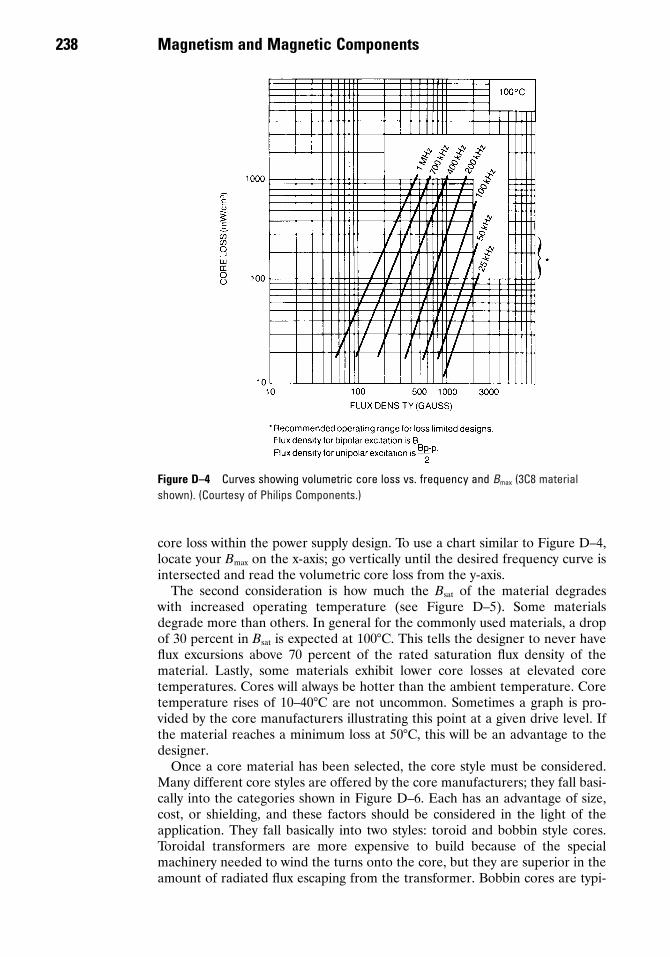
core loss within the power supply design. To use a chart similar to Figure D–4,locate your Bmax on the x-axis; go vertically until the desired frequency curve isintersected and read the volumetric core loss from the y-axis.
The second consideration is how much the Bsat of the material degrades with increased operating temperature (see Figure D–5). Some materialsdegrade more than others. In general for the commonly used materials, a dropof 30 percent in Bsat is expected at 100°C. This tells the designer to never haveflux excursions above 70 percent of the rated saturation flux density of the material. Lastly, some materials exhibit lower core losses at elevated core temperatures. Cores will always be hotter than the ambient temperature. Coretemperature rises of 10–40°C are not uncommon. Sometimes a graph is pro-vided by the core manufacturers illustrating this point at a given drive level. Ifthe material reaches a minimum loss at 50°C, this will be an advantage to thedesigner.
Once a core material has been selected, the core style must be considered.Many different core styles are offered by the core manufacturers; they fall basi-cally into the categories shown in Figure D–6. Each has an advantage of size,cost, or shielding, and these factors should be considered in the light of theapplication. They fall basically into two styles: toroid and bobbin style cores.Toroidal transformers are more expensive to build because of the specialmachinery needed to wind the turns onto the core, but they are superior in theamount of radiated flux escaping from the transformer. Bobbin cores are typi-
238 Magnetism and Magnetic Components
Figure D–4 Curves showing volumetric core loss vs. frequency and Bmax (3C8 materialshown). (Courtesy of Philips Components.)

cally less expensive to build than toroids, which is a distinct advantage, but costmore than toroids for the basic core parts. Some of these considerations areoutline in Table D–3. Pot cores and their derivatives (PQ, RS, etc.) are expen-sive to buy, but are inexpensive to have a transformer built. Pot cores offer goodmagnetic shielding of the windings and the gap. Unfortunately, the lack ofairflow around the windings causes them to operate at a higher temperature. E-E and E-I cores are less expensive than pot cores and have a generally largerwinding area. Since, in the winding of transformers, the winding area is whattypically determines a core size, this makes E-E and E-I cores the most preva-
Magnetism and Magnetic Components 239
Figure D–5 Curve illustrating the degradation of Bsat with core temperature (3C8 materialshown). (Courtesy of Philips Components.)

lent choice among designers. The windings are exposed to the air so that thewindings operate at cooler temperatures, but radiate more to the environmentbecause of the exposed air-gap.
Trade-offs in basic core cost, final transformer cost, and RFI are the primaryconsiderations.
240 Magnetism and Magnetic Components
Figure D–6 The common styles of magnetic cores.
Appendix E. Noise Control andElectromagnetic Interference
241
Controlling high frequency noise generation and radiation is the blackest of the “black box” art in switching power supply and product-system design. It isa subject that warrants a book all to itself and it is the final area that will inter-fere with the release of your product into the market. This appendix cannot ade-quately cover the subject, but will overview the major considerations involvedwith product design.
Most companies cannot afford the expense of setting up a noise testing lab-oratory suitable for regulatory agency testing. The equipment is expensive andthe operators must have special training. It is recommended that a companyemploy a regulatory testing consultant company to help it through this phase ofthe program. The majority of products initially submitted for RFI/EMI approvalfail one or both of the radiated or conducted EMI tests. Almost always thedesign needs last-minute changes in order to pass the tests. The consultant engi-neers have been through this exercise many times before and are familiar withthe problem areas and their solutions.
With help from this appendix, and Sections 3.12 and 3.14, it is hoped thatyour design will at least have an acceptable PC board layout, input EMI filter,and enclosure design that can serve as a basis for minor modifications at thetime of testing. The PC board layout is the first major thing that the designercan do to minimize the effects of noise. The use of waveshaping techniques arethe second, and the enclosure design is the third most important thing. Onegeneral rule is that if you design for the most stringent of your regulatoryrequirements, you will be better off when it comes time to test the product. Mostof the countries in the world are “harmonizing” on their testing limits withintheir specifications.
If one passes one country’s EMI/EMC specification, it is likely that theproduct will have no trouble in passing another country’s requirements.
E.1 The Nature and Sources of Electrical Noise
Noise is created whenever there are rapid transitions in voltage and/or currentwaveforms. Many waveforms, especially in switching power supplies, are peri-odic. That is, the signal that contains pulses with high frequency edges repeatsitself at predictable pulse repetition frequencies (PRF). For rectangular pulse-trains, the inverse of the period dictates the fundamental frequency of the wave-form itself. The fourier conversion of a rectangular waveform generates a wealthof harmonics of this fundamental frequency. The inverse of twice the edge

risetime or falltime of these pulses are estimates of the spectral fundamentalfrequency of the edges. This is typically in the megahertz range and their har-monics can go much higher in frequency.
In PWM switching power supplies, the pulsewidth of the rectangular wave-shape is continuously changing in response to the supply’s operating conditions.The result is typically an almost white noise energy distribution that exhibitssome peaks and the amplitude rolls off with higher frequencies. Figure E–1 isa near-field radiated spectrum of an off-line PWM flyback switching powersupply with no snubbing. As one can see, the spectral components extend wellover 100MHz (far right) and would interfere with consumer electronics equip-ment, if not filtered and shielded.
Quasi-resonant and resonant transition switching power supplies have a muchmore attractive radiated spectral shape. This is because the transitions areforced to be at a lower frequency by the resonant elements, hence only the lowfrequency spectral components are exhibited (below 30 MHz). The lower rateof change during the transitions are responsible for behavior. The higher fre-quency spectral components are almost non existent. The near-field radiatedspectrum of a quasi-resonant, flyback converter are shown in Figure E–2. Thequasi-resonant and soft switching families of converters are much “quieter” andeasier to filter.
Conducted noise, that is, noise currents that exit the product enclosure viathe power lines and any input or output lines, can manifest itself in two forms:common-mode and differential-mode. Common-mode noise is noise that exitsthe case only on the power lines and not the earth ground and can be measuredwith respect to the power lines (refer to Figure E–3a). Differential-mode noiseis noise that can only be measured from the earth ground to one of the powerleads. Noise currents are actually exiting via the earth ground lead. Its modelcan be seen in Figure E–3b. Each mode of noise can only be controlled by spe-cific filter topologies and in each power supply design may require two types ofinput filtering. These filters have inductors and capacitors which are called “X”and “Y” elements. The X elements go across the power lines filtering the
242 Noise Control and Electromagnetic Interference
Figure E–1 The radiated spectrum of a typical off-line PWM flyback converter.

Noise Control and Electromagnetic Interference 243
common-mode noise artifacts and the Y elements go between the power linesand earth ground filtering the differential noise artifacts.
Regulatory approval bodies check for both radiated and conducted noiseduring their certification testing. Radiated noise is checked by locating a cali-brated antenna and receiver at a specified distance (1 meter) from the productand plotting the resulting spectrum well into the GHz region. Radiated noisecauses interference with other equipment, but conducted noise uses the powerand I/O lines to radiate its noise and therefore is also checked. Conducted noiseis checked by coupling into the input power lines via a high-frequency currenttransformer and the resultant spectrum is checked beyond 1GHz.
E.2 Typical Sources of Noise
Noise, especially radiated noise, can be reduced by understanding its sourcesand what design techniques can reduce its effects. There are several major
Figure E–2 The radiated spectrum of a ZVS QR off-line flyback converter.
Figure E–3 Common-mode and differential noise models: (a) common mode; (b) differentialmode.

sources of noise within a PWM switching power supply that create the majority of radiated and conducted noise. These sources can be easily locatedand their design can be modified to reduce the noise generation of the powersupply.
Noise sources are part of noise loops which are printed circuit board con-nections between high-frequency current sinks and current sources. Followingthe PC board design practices in Section 3.14 will help greatly in reducing theradiated RFI. Appreciation of the high-frequency characteristics of the commoncomponents and PC boards is needed.
The first major source of noise is the input power circuit, which includes the power switch, the primary winding of the transformer, and the input filter capacitor. The input filter capacitor provides the entire trapezoidal current waveforms needed by the power supply, since the input line is alwaysheavily filtered with a bandwidth much less than the operating frequency of the power supply. The PCB traces must be as physically short and as fat as possible. Fat traces have lower inductance than thin traces. The trace length dictates the frequencies above which noise will be easily radiated into the environment. Shorter traces radiate less energy at the higher frequencies. The input filter capacitor and the power switch should be next to the trans-former to minimize the trace lengths. A high-frequency ceramic or film capacitor also should be placed in parallel with any aluminum electrolytic or tantalum input capacitor since they have poor high-frequency characteris-tics. The worse the ESR and ESL characteristics of the input filter capacitor,the more high frequency noise energy the power supply will draw directly from the power line, thus promoting poor common-mode conducted EMIbehavior.
Another major source of noise is the loop consisting of the output rectifiers,the output filter capacitor, and the transformer secondary windings. Once again,high-peak valued trapezoidal current waveforms flow between these compo-nents. The output filter capacitor and rectifier also want to be located as phys-ically close to the transformer as possible to minimize the radiated noise. Thissource also generates common-mode conducted noise mainly on the outputlines of the power supply.
One subtle, but major noise source is the output rectifier. The shape of thereverse recovery characteristic of the rectifiers has a direct affect on the noisegenerated within the supply. The abruptness or sharpness of the reverse recov-ery current waveform is often a major source of high-frequency noise. An abruptrecovery diode may need a snubber placed in parallel with it in order to lowerits high-frequency spectral characteristics. A snubber will cost the designer inefficiency. Finding a soft recovery rectifier will definitely be an advantage in thedesign.
One structure that encourages the conduction of differential-mode noise is the heatsink. Heatsinks are typically connected to earth ground as a protection to the operator or service person. Any power switch or rectifier that is bolted to a heatsink allows capacitively coupled noise into the heatsinkthrough the insulating pad. This noise then exits the case via the green, earthground wire. One way of reducing the injection of this noise onto the ground is to use a power device insulator pad with an embedded foil pad. This reduces the mounting capacitance by pacing two capacitor in series, or thedesigner can connect the internal foil layer to the internal power supplycommon.
244 Noise Control and Electromagnetic Interference

Noise Control and Electromagnetic Interference 245
E.3 Enclosure Design
Product enclosure should act as an electromagnetic shield for the noise radiated by the circuitry within the package. A metal-based, magnetic materialshould be used in the enclosure construction. The material should be iron, steel,nickel, or Mu metal. For plastic enclosures, there are an assortment of con-ductive paints that can be used to add EMI/RFI shielding to the case. Also, anyvent openings may need magnetic screening covering the openings.
The philosophy of any EMI shield is to encourage eddy currents to flow withinthe surfaces, thus dissipating the noise energy. Also, the assembled enclosureshould act as a gaussian enclosure where there is good electrical conductiontotally around the enclosure. So removable hatches and enclosure membersneed very good electrical connections around their peripheries. RF gasketing issometimes used in particularly troublesome cases.
Leads that enter or exit the enclosure ideally should have their associatedEMI filters at the point of entry or exit from the enclosure. Any unfilteredleadlengths that run within the enclosure will inductively pick-up noise withinthe case and allow it to exit the case, thus making any EMI filtering less effec-tive. Likewise, any unfiltered leads within the case will radiate any transientsfrom outside the case into the case, which may affect the static discharge behavior of the contained circuits to external static events.
E.4 Conducted EMI Filters
There are two types of input power buses. DC power buses are single-wirepower connections such as found in automobiles and aircraft. The ground con-nection forms the other leg of the power system. The other form of input con-nection is the ac, or two or three-wire feed systems as found in ac power systems.The design of the EMI filter for dc systems is covered in Section 3.12 and takesthe form of a simple L-C filter. All the noise is common-mode between thesingle power wire and the ground return. The dc filter is much more compli-cated, because of the parasitic behavior of the components involved.
To design a filter for the input of a switching power supply, the designer firstneeds to know which of the regulatory specifications is appropriate for theproduct. The specifications dictate the conducted and radiated EMI/RFI limitsthe product must meet to be sold into the particular market. A company’s marketing department should know which areas of the world the product willbe sold and hence the designers can determine the requirements that are appro-priate. It is always a good idea to design for the most stringent specification thatis applicable to your market.
The purpose of an input conducted EMI filter is to keep the high-frequencyconducted noise inside the case. The main noise source is the switching powersupply. Filtering on any of the input/output (I/O) lines is also important to keepnoise from any internal circuit, like microprocessors, inside the case.
Design of the common-mode filterThe common-mode filter essentially filters out noise that is generated betweenthe two power lines (Hot and Neutral or H1 and H2). The common-mode filterschematic is shown as part of Figure E–4.

In the common-mode filter the windings of the “transformer” are in phase,but the ac currents flowing through the windings are out of phase. The result isthat the common-mode ac flux within the core for those signals that are equaland opposing phases on the two power lines cancel out.
The problem with designing the common-mode filter is that at high frequen-cies, where one wants and needs the filtering, the ideal characteristics of thecomponents are compromised by their parasitic behavior. The major parasiticelement is the interturn capacitance of the transformer itself. This is the smallcapacitance that exists between all windings, where the voltage difference(volts/turn) between turns behaves like a capacitor. This capacitor, at high fre-quency, effectively acts as a shunt around the winding and allows more high-frequency ac current to go around the windings. The frequency at which thisbecomes a problem is above what is called the self-resonance of the winding. Atank circuit is formed between the winding inductance itself and this distributedinterturn capacitance. Above the self-resonance point the effects of the capacitance become larger than the inductance which then reduces the level ofattenuation at high frequencies. The effect of this within the common-modefilter can be seen in Figure E–5. Its affect can be reduced by purposely using alarger X capacitor. The self-resonance frequency is the point where the great-est possible attenuation for the filter is exhibited. So by choosing the windingmethod of the transformer, one can locate this point on top of a frequency thatneeds the greatest filtering, such as a harmonic peak in the unfiltered systemnoise spectrum.
Another area of concern is the “Q” of the filter at self-resonance. If the Q istoo high, or in other words, the damping factor is too low, the filter will actu-ally generate noise in the form of narrow-band ringing. This can be dealt withduring the design.
Some major transformer manufacturers build standard off-the-shelf compo-nents used in the design of common-mode filter transformers such as Coilcraft(Cary, IL). These transformers have various inductance values, and currentratings and also provide the needed creepage dimensions. This can make thedesigner’s job a lot easier.
The initial common-mode filter component values can be determined in astep-by-step process (like everything else in this book). To begin this process,either a baseline measurement of the unfiltered conducted noise spectrum is
246 Noise Control and Electromagnetic Interference
Figure E–4 A complete third-order, input EMI filter (common-mode and differential-mode).

Noise Control and Electromagnetic Interference 247
needed or some assumptions need to be made. This is in order to know howmuch attenuation is needed and at what frequencies. Obviously, making themeasurement will yield a good result (with minor tweeks) the first time. Assum-ing that one needs a particular filter response on paper may lead to additional“fudging” of the circuit on the test table.
A reasonable beginning is that one needs about 24dB of attenuation at theswitching frequency of the switching power supply. This, of course, should bemodified in response to the actual conducted noise spectral shape. One deter-mines the corner frequency of the filter by
or
where: fc is the desired corner frequency of the filter.fsw is the operating frequency of the power supply.
For this example, the switching frequency is assumed to be 50kHz. The cornerfrequency to produce -24dB of attenuation at this point is
One assumes that the line impedance is 50ohms (because that is what theLISN test’s impedance is). This impedance is then the damping element withinthe reactive filter circuit.
Choosing the damping factorThe minimum damping factor (z) should be no less than 0.707. Less than thatwould allow ringing to occur and produce less than 3 dB of attenuation at thecorner frequency.
fC kHz kHz= ( ) =-Ê
ËÁˆ¯50 10 12 5
24
40 .
f fAtt
C SW= ◊ÊËÁ
ˆ¯10 40
Attenuation dB Log C
SW
-( ) = ÊËÁ
ˆ¯40
F
f
Figure E–5 Frequency response of a second-order common-mode filter (L = 1 mH).

Calculating the initial component values
Choosing “real world” available componentsThe largest value of capacitor that is available in the 4KV voltage rating is 0.05mF. This is 27 percent of the calculated value. In order for the corner fre-quency to remain the same, the inductor value should be increased by a factorof 3.6. This would make the value 3.24 mH. The damping factor is directly pro-portional to the value of the inductance so the resultant damping factor is 2.5which is acceptable.
The closest Coilcraft common-mode inductor part number is E3493 and itsself-resonance frequency is 1MHz. The calculated capacitors are what are typically called “Y” capacitors. These are placed between each phase and theearth ground and must meet the full HIPOT test voltage of 2500 VRMS. “X”capacitors are the ones that are placed between the power lines and need onlymeet the 250VRMS rating of the power line and be able to withstand any surgethat may be anticipated. Choosing the value of the X capacitors is mainly arbi-trary and usually they fall in the 0.001 to 0.5mF range.
One can reasonably expect this filter to provide a minimum of 60dB of atten-uation between the frequencies of 500kHz and 10MHz.
Once the component values have been calculated, the physical constructionof the transformer and the PCB layout become critical for the effectiveness ofthe filter stage. Magnetic coupling due to stray inductive pick-up of high-frequency noise by the traces and components can circumvent the filter alltogether. Added to this is the fact that the common-mode filter choke looksmore and more capacitive above its self-resonance frequency. The net result isthe designer needs to be concerned about the high-frequency behavior of thefilter typically above 20 to 40MHz.
Physical layout of the PCB is important. The filter should be laid out in alinear fashion so that the input portion of the filter is physically distant from theoutput portion. Large, low-inductance traces should be also used, but keep inmind the creepage requirements of the regulatory specifications.
Sometimes the high-frequency attenuation is insufficient to meet the specifi-cations and a third pole needs to be added to the EMI filter. This filter is typically a differential-mode filter and will share the Y capacitors from thecommon-mode filter. Its corner frequency is typically the same as the common-mode filter. This filter is made up of a separate choke on each power line, andis placed between the input rectifiers and the common-mode filter.
The differential-mode filter should have a lower damping factor than thecommon-mode because the combined damping response of the entire filtersection would be too sluggish if higher damping factors were used. A dampingfactor of a minimum of 0.5 is acceptable.
Calculating the differential-mode choke value
LR
f
H
L
C
dkHz
=◊
◊=
( )( )( )
=
z
p pm
2
50 0 5
2 12 5318
.
.
Cf LC
=( )
=( )[ ] ( )
1
2
1
2 12 5 9002 2
p p m. kHz H
L
R
f=
◊
◊=
( )( )( )
=L
C kHzH
z
p pm
50 0 707
12 5900
.
.
248 Noise Control and Electromagnetic Interference

The addition of this stage of filtering will bring the very high-frequency attenuation under control and further attenuate any differential-mode noise on the earth ground lead. It will also produce a combined attenuation of -36dB at the switching frequency of the power supply.
Real-world considerationsIf one was to build the inductive elements instead of buying off-the-shelf partsfrom a manufacturer, the following guidelines are common industry practices.
Common-mode chokes (transformers)
1. A toroid is best for this application because it produces very little straymagnetic fields.
2. A high permeability ferrite is used such as the W material from Magnetics, Inc. which has a permeability of 10,000.
3. If an E-E core is used (which is a common choice), there should be no air-gap and the mating surfaces of the cores must be polished. Any surfaceimperfections would lower the permeability.
4. The bobbin should be a two-section bobbin and not be completely filledwith windings. A 2mm space from the outside surface of the bobbin isrequired for the 4mm creepage requirement of VDE.
Differential-mode chokes
1. These are wound on separate cores (not mutually coupled).2. Use a powdered iron material such as available from MicroMetals
(Evanston, IL).3. Bar cores are typically used because of cost.
Noise Control and Electromagnetic Interference 249

Appendix F. Miscellaneous Information
250
This appendix contains a potpourri of miscellaneous information that may beneeded occasionally.
F.1 Measurement Unit Conversions
This is by far the most confusing area of global cooperation. There are thosecountries which have completely converted to metric and use the MKS (meters-kilogram-second) system, there are countries that use a hybrid metric systemwith a mixture of metric units, such as Japan, and then there is the U.S. whichmixes metric CGS (centimeter-gram-second) system with old English units suchas inches, mils, and circular mils. All three systems are used by major core manufacturers around the world. The designer, depending upon where he orshe wants to buy magnetics, must be extremely cautious as to which equationshe or she is using and the units of measurement of the variables each particu-lar equation. Core manufacturers rarely elaborate on their units of measure-ment. As an aide to the designer, the conversion constants between the systemsare given below.
Flux Density1 Tesla (Webers/m2) = 104 Gauss (Webers/cm2) (Europe)1 Gauss (Webers/cm2) = 10-4 Tesla (Webers/m2) (USA)1 milliTesla = 10-3 Tesla (Japan)1 milliTesla = 10 Gauss (Japan)
Linear Measurements1 centimeter = 0.394 inches1 millimeter = 0.0394 inches1 inch = 2.54 centimeters1 inch = 25.4 millimeters
Area Measurements1 square inch (in2) = 6.45 square centimeters (cm2)1 in2 = 645 square millimeters (mm2)1cm2 = 0.155 in2
1mm2 = 0.00155 in2
1 circular mil = 7.854 ¥ 10-7 in2
1 circular mil = 5.07 ¥ 10-6 cm2
1 in2 = 1.273 ¥ 106 circular mils1cm2 = 1.974 ¥ 105 circular mils

F.2 Wires
The specification of wires can be confusing. All wires diameters are based uponthe American Wire Gauge (AWG) table, published in the early 20th century.The metric countries directly converted these dimension (inches) to millimetersand created what is now the IEC R20 wire table. This is shown below in bothmeasurement systems in Table F–1.
The R20 chart is being eventually replaced with the IEC R40 standard asshown in Table F–2. The wire diameters are still very close to the AWG table.
Miscellaneous Information 251

Skin effect is the apparent increase in wire resistance when high-frequencyac currents are passed through them. A wire’s real resistance when involvinglosses within a switching power supply is given in Equation F.1.
Rtotal = RDC + RAC (F.1)
RAC is the result of multiplying the below ratio with the dc resistance for a roundcopper wire such as round magnet wire. The equation below is the percent ofincrease of the ac resistance over the dc resistance for a single strand of roundcopper wire in open air.
252 Miscellaneous Information

(F.2)
where d is the diameter of the wire in centimeters.f is the frequency of the fundamental frequency of the current
waveform in hertz.
As one can see, the larger-diameter wires suffer a much more rapid degra-dation in ac resistance with increasing frequency than do smaller-diameterwires. So it is advantageous to use multiple strands of smaller wires instead ofone large diameter wire. The ac current density of the smaller wires (>30AWG)can actually be pushed to two to three times the assumed current density usedin the charts because their surface area to cross-sectional area ratio is muchgreater.
The ac resistance increase due to skin effect given above should be consideredas a minimum. When wires are placed next to one another and placed in layerswithin a transformer, the near field magnetic effects between wires furthercrowd the current density into even smaller areas within the wire’s cross-section.For instance, when wires are wound next to one another, the current is pushedaway from the points of contact along the surfaces of the wires to areas orthog-onal to the winding plane. When layers are placed on top of one another theinner layers show much greater degradation in apparent resistance than do theoutermost layers.
For estimation purposes, using the above resistance numbers will be sufficient.
R
Rd fAC
DC
ª ◊ ◊ ◊0 47. p
Miscellaneous Information 253


References
255
Ben-Yaakov, Sam and Gregory Ivensky, Passive Lossless Snubbers for High FrequencyPWM Converters, Seminar 12, APEC 99.
Balogh Laszlo, Practical Considerations for MOSFET Gate Drive Techniques in HighSpeed, Switch-mode Applications, Seminar APEC99. March 1999.
Brown, Marty, “Laying Out PC Boards for Embedded Switching Supplies,” ElectronicDesign, December 6, 1999.
Brown, Marty, Practical Switching Power Supply Design, Academic Press, 1990.
Carsten, Bruce, Avoiding the EMI Accident, Seminar APEC99, March 1999.
Carsten, Bruce, Switchmode Design Techniques Above 500kHz, High Frequency PowerConversion Conference, May 1986.
Carsten, Bruce, High Frequency Losses in Switchmode Magnetics, High FrequencyPower Conversion Conference, May 1986.
Li, Alan, Brij Mohan, Steve Sapp, Izak Bencuya, and Linh Hong, Maximum PowerEnhancement Techniques for SuperSOT-6 Power MOSFETs, Fairchild Ap NoteAN1026, April, 1996.
Martin, Robert F., Harmonic Currents, Compliance Engineering—1999 AnnualResources Guide, Cannon Communications, LLC, 103–107.
Venable, H. Dean, The K Factor: A New Mathematical Tool for Stability Analysis andSynthesis, POWERCON March 1983.


AAC voltage nodes, 98Active clamps, 148–49Active output stages (Synchronous
Rectifiers), 60–61Ambient temperature, 188American Wire Gauge (AWG) table, 251Amplifier compensation designs,
common error, 206–19Amplifiers
error, 75, 198locating compensating poles in error,
212, 215, 217–18locating zeros in error, 212, 215,
217–18voltage error, 12, 71
Average current foldback, 72AWG (American Wire Gauge) table, 251
BB-H curves, 232–35Base drive transformers, 50–52Base drives, fixed, 63Base speed-up capacitors, 64Bias circuit designs, start up and IC,
80–82Bifilar wound windings, 48Bipolar power transistor drive circuits,
63–66Black box
considerations for switching powersupplies, 34–37
predesign considerations, 114–15Board-level converters, 3, 28Bode responses of circuits in switching
power supplies, 196–200Boost-mode converters, 22, 24–26, 31Boost power factor correction circuit, 222Bootstrap start-up circuits, 80, 126Brownout conditions, 91Buck-boost converters, 31Buck/boost power factor correction
circuit, 222Buck converters, 30, 100–5, 163–70Buck power factor correction circuits, 221
CCanadian Standards Agency (CSA), 52Capacitances, inter-turn, 54
Capacitive input filter, waveforms of, 221
Capacitorsbase speed-up, 64input filter, 102–3, 165losses associated with filter, 139output, 101–2, 164–65paralleling filter, 99resonant, 160
Catch diodes, 23, 101CGS (centimeter-gram-second), 250Choke input filters, 22, 198Choke value, calculating differential-
mode, 248–49Chokes
common-mode, 249designing dc filter, 48–50designing forward-mode filter, 46–47designing mutually coupled forward-
mode filter, 47–48differential-mode, 249
Circuit designs, start up and IC bias,80–82
Clamps, active, 148–49Common-mode chokes, 249Common-mode filters, designing, 245–47Compensating poles, locating, 212, 215,
217–18Compensation
designing feedback loop, 119–20,174–76, 181–83, 196–219
designing voltage feedback, 129–31feedback loop, 12, 111–13, 196–219in-band gain limiting, 213pole-zero, 212–16single-pole, 207–11slope, 127–282-pole-2-zero, 216–19
Compensation designs, common erroramplifier, 206–19
Compensation method, pole-zero, 214Components
choosing real world available, 248losses associated with magnetic,
140–42Conduction losses, 136–8Conduction-mode controller, critical, 225Conductors, fields around, 233Continuous mode of operation, 25
Index
257

Control IC, power factor, 223Control method, selecting optimum,
72–75Control, miscellaneous modes of, 74–75Control-to-output characteristics, 201–5
defining, 168Controller IC s selecting, 70–75Controllers
critical conduction-mode, 225switch-mode, 109
Converters, PWM design examples,10 watt synchronous buck, 163–70
design examples, 16328 watt PWM flyback, 105–1365 watt multiple-output flyback,
114–22280 watt half-bridge, 122–33
slope compensation, 127–28transformer design, 123–24transformer winding technique, 124
board-level, 28board-level 10 watt step-down buck,
100–105boost, 26, 31boost-mode, 24–26buck, 30buck-boost, 31current-mode controlled forward-mode
compensation, 203–5flyback, 26, 32forward-mode, 22–24full-bridge, 29, 34half-bridge, 29, 33one-transistor forward, 32parasitic elements within all, 142–43phase modulated PWM full-bridge,
161–62push-pull, 29, 33QR (quasi-resonant), 151–85step down, 30step-down, 22step-up, 31synchronous buck, 163–70transformer-isolated forward, 24transformer-isolated QR (quasi-
resonant), 158voltage/current-mode controlled
flyback compensation, 213, 215voltage-mode controlled flyback
compensation, 203–5voltage-mode controlled forward-mode
compensation, 201–3ZVS QR, 154–55ZVS QR current-mode controlled
flyback, 170–76ZVS QR off-line half-bridge, 176–85
258 Index
Core, DC bias, 47Core imbalance defined, 29Core loss vs. frequency, 238Core material and style, selecting, 236–
40Core materials used within industry,
common, 237Core styles and merits, 239Cores
common styles of magnetic, 240determining sizes of magnetic, 38–40
Corner frequencies, 196–97Critical conduction-mode controller, 225Cross-regulation, 55, 61CSA (Canadian Standards Agency), 52Current error voltage, 71Current foldback, average, 72Current loops, major (PCB), 93–96Current loss, eddy, 236Current mode control, 74
hysteretic, 74Current-mode controlled forward-mode
converters, 203–5Current; See also Overcurrent
limiting rectifier reverse recovery,148–50
punch-through, 61Current sense resistors, 167Current sensing circuit, designing, 127,
229Current sensing, instantaneous, 71–72Curves, B-H, 232–35
DDamping factor, choosing, 247–48DC-DC converters, 89DC filter chokes, designing, 48–50DC resistive losses, 141Differential-mode choke values,
calculating, 248–49Differential-mode chokes, 249Differentiators, zero, 198Digital voltmeters (DVMs), 96, 187Diodes
catch, 23, 101radial-leaded, 191–92synchronous, 164
Discontinuous-mode of operation, 25Discrete linear regulators designs, 15Distortion, total harmonic, 224Distributed power system, 3Drive circuits, bipolar power transistor,
63–66Drive transformers, designing gate,
125–26, 167Driver sections, designing, 63–70

Index 259
Drives, fixed base, 63Dropout voltage defined, 13
EEddy current loss, 236Electrical noise, nature and sources of,
241–43Elements, parasitic, 141EMI (electromagnetic interference), 21,
93, 96, 98, 135, 145, 223and noise control, 241–49
EMI/EMC, 241EMI filters, 48, 87, 89–90, 241, 245, 248
conducted, 245–49designing input, 120–22, 133, 230–31
EMI/RFI, 192, 224, 245Enclosure design, 245Equivalent series inductance (ESL), 62,
139Equivalent series resistance (ESR), 62,
89, 99, 102, 139, 203, 216Error amplifiers, 75, 198
compensation, design, 196–219voltage, 71
Error voltage, current, 71Error voltages, 71ESL (equivalent series inductance), 62,
139ESR (equivalent series resistance), 62,
89, 99, 139, 203, 216External sources, synchronization of
power supplies to, 90–91
FFaraday’s law, 234FBSOA (forward-biased safe operating
areas), 145Feedback
isolated, 78voltage, 109–10, 129
Feedback circuitsdesigning voltage, 75–80, 180–81,
229–30voltage, 118
Feedback compensation, designingvoltage, 129–31, 196–219
Feedback loop compensation, 12, 111–13,196–219
designing, 119–20, 174–76, 181–83Feedback loops, designing voltage,
118–19, 128–29, 196–219Feedback voltage, 71Fields around conductors in free air, 233Filar winding, 56Filter capacitors
input, 102–3, 165
losses associated with, 139paralleling, 99
Filter chokesdesigning dc, 48–50designing Forward-mode, 46–47designing mutually coupled forward-
mode, 47–48Filter circuits, designing input, 131–32Filter section
designing input EMI, 120–22, 230–31
designing input rectifier, 84–90designing output, 116–17input, 110output, 108–9
Filterschoke input, 22, 198conducted EMI, 245–49designing common-mode, 245–47designing input EMI, 133designing output, 124–25, 178–79EMI, 48, 87, 89–90, 241, 245, 248high-pass, 198output, 61–63Q of, 246RC low-pass, 197single-pole filter, 199two-pole, 198waveforms of capacitive input, 221
Fixed base drivers, 63Floating linear regulators, 18–20Flux density, 232, 234, 237Flux, lines of, 232Flyback converters, 26, 32
28 watt PWM, 105–1365 watt multiple-output, 114–22voltage/current-mode controlled, 213,
215voltage-mode controlled, 203–5ZVS QR current-mode controlled
flyback converters, 170–76Flyback topology, 29Flyback transformers
designing, 42–45, 105–8, 171–72secondary arrangements, 45
FMEA (failure modes and effectsanalysis), 83
Forward-biased safe operating areas(FBSOA), 145
Forward convertersbuck, 30full-bridge, 34half-bridge, 33one-transistor, 32push-pull, 33transformer-isolated, 24

Forward-mode converters, 22–24current-mode controlled, 203–5voltage-mode controlled, 201–3
Forward-mode filter chokesdesigning, 46–47designing mutually coupled, 47–48
Forward-mode secondary windingarrangements, 43
Forward-mode transformers, designing,40–42
Frequenciescore loss vs., 238corner, 196–97flux density limits vs., 237natural resonance, 157resonance, 197
Frequency control, variable, 74–75Frequency responses, 199–200Full-bridge converters, 29, 34
phase modulated PWM, 161–62
GGain limiting, single-pole compensation
with in-band, 211–12Gate drive transformers, 50–52
designing, 125–26, 167Gauss, 234Ground, control, 96Grounds inside switching power supply,
96–98
HHalf-bridge converters, 29, 33
280 watt, 122–33ZVS (zero voltage switched) QR
(quasi-resonant) off-line, 176–85Harmonic distortion, total, 224Harmonics, power factor and, 223Headroom voltage defined, 13Heatsinks
determining smallest, 193–94maximum ambient temperature
without, 194–95power packages not on, 190power packages on, 189–90thermal models for transistors on, 189
Hiccup-mode start-up, 73, 80High-pass filters, 198Hysteresis loss, 234, 236Hysteretic control, voltage, 73, 74Hysteretic current mode control, 74
II/O (input/output), 245IC bias circuit designs, start up and,
80–82
260 Index
ICs (integrated circuits), 9current-mode control, 74–75power factor control, 223selecting controller, 70–75voltage-mode control, 72
IEC (International EngineeringConsortium), 52
IGBTs as power switches, 63, 69–70In-band gain limiting, single-pole
compensation with, 211–12Inductance, winding for low leakage
inductance, 54–55Inductor design, 226–28Inductors, saturable, 148–50Input circuit, designing voltage
multiplier, 229Input EMI filter section, designing, 110,
120–22, 131–32, 230–31Input EMI input filters, designing,
133Input filter capacitors, 102–3, 165Input filters
choke, 198waveforms of capacitive, 221
Input low voltage inhibit, 91Input/output (I/O) Noise, 245Input, power factor corrected, 221Input rectifier/filter section, designing,
84–90Instantaneous current sensing, switching
power supplies, 71–72Integrated circuits (ICs); See ICs
(integrated circuits)Integrated gate bipolar transistors
(IGBTs), 63Integrated power system, 3Inter-turn capacitance, 54Interleaving windings, 56–57International Engineering Consortium
(IEC), 52Isolated feedback, 78
JJunction temperatures
maximum operating, 187of rectifiers, 195
Junction-to-air, thermal resistance, 188,190
Junction-to-case, thermal resistance,188–89
Junction-to-lead, thermal resistance, 188,192
LL-C tank circuits, designing, 178Lead temperatures, 195

Index 261
Leakage inductance, winding for low,54–55
Line impedance stabilization network(LISN), 224–25, 230, 247
Linear power supply design examples,14–20
Linear regulatorsdiscrete designs, 15floating, 18–20general considerations, 12–14introduction to, 11–20operation, 11–12
LISN (line impedance stabilizationnetwork), 224–25, 230, 247
Litz wires, 47Load regulation, output, 76Loop compensation
designing feedback, 119–20, 174–76feedback, 111–13, 196–219
Loopsdesigning voltage feedback, 118–19,
128–29major current (PCB), 93–96minor (B-H), 140, 233, 235
Lossesassociated with filter capacitors, 139associated with magnetic components,
140–42, 236associated with output rectifiers,
137–38associated with power switches, 136–37conduction, 136–38DC resistive winding, 141eddy current, 140, 236hysteresis, 140, 234, 236within PWM switching power supply,
135–43quiescent, 139–40reducing major, 143–45skin effect resistive, 141switching, 136–38
Lossless snubbers, 145–46Low dropout regulators, 14Low-pass filter, RC, 197Low voltage inhibit (LVI), 81, 91
MMagnetic components
losses associated with, 140–42magnetism and, 232–40
Magnetic corescommon styles of, 240determining sizes of, 38–40
Magnetic elements, 37–56design flow of, 37–38
Magnetic field strength (H), 234
Magnetic theory applied to switchingpower supplies, 232–36
Magnetism and magnetic components,232–40
Major losses, reducing, 143–45Maximum operating junction
temperature, 187Measurement unit conversions, 250Metal-oxide varistors (MOVs), 90Minor-loop magnetic, 140MKS (meters-kilogram-second), 250Modes of control, 74–75
current-mode, 74current-hysteretic, 74hiccup, 73hiccup restarting, 80voltage-hysteretic, 73voltage-mode, 73
MOSFET, clamp switch, 148MOSFET power switches, power, 66–
69MOSFETs, 14, 29, 50, 57, 61, 71, 93, 126,
139, 142, 159selection of synchronous rectifier, 164
MOVs (metal-oxide varistors), 90Multiple-output flyback converters, 65
watt, 114–22Multiple output sensing, 77–78Multiplier PFC, 229
NNatural resonance frequency defined,
157Nodes, AC voltage, 98Noise
nature and sources of electrical,241–43
typical sources of, 243–44Noise control and EMI (electromagnetic
interference), 241–49Nonisolated single-output switching
power supply, 76Nonisolated topologies, 30–31
OOne-transistor forward converters, 32Optoisolators, 78Optoisolated feedback, 79–80Output capacitors, 101–2, 164–65Output-filter section, 61–63, 108–9
designing, 116–17, 124–25, 178–79Output load regulation, 7, 76Output protection schemes, 82–84Output rectifiers, losses associated with,
137–38Output ripple voltage, 6, 62

Output sensing, multiple, 77–78Output stages
active, 60–61designing, 56–63passive, 58–59
Output voltage shut-down, 93Overcurrent protection
circuits, 183–85pulse-to-pulse, 73
Overload protection, constant powerform of, 74
PParasitic behavior, major sources of, 144Parasitic elements within all converters,
142–43Parts, surface mount thermal, 192–93Passive lossless snubbers, 146–48Passive output stages, 58–59Passive rectification, 57PCBs (printed circuit boards), 8–9, 93,
142, 231, 248creating for switching power supplies,
99–100laying out, 93–100
PFC circuits, designing, 224–25PFCs (power factor corrections), 85,
220–31Phase modulated PWM full-bridge
converters, 161–62Pole-zero compensation, 212–16Poles
defined, 196locating compensating, 104–5, 168–70
Post regulators, 14Power dissipated, maximum, 194–95Power factor and harmonics, 223Power factor control IC, 223Power factor corrected input, 221Power form of overload protection,
constant, 74Power MOSFET power switches, 66–69Power packages not on heatsinks, 190Power packages on heatsinks, 189–90Power signal, impending loss of, 92Power supplies
black box considerations for switching,34–37
building-block approach to, 8–9building-block approach to PWM
switching, 26–28creating PCBs for switching, 99–100defining open loop response of
switching, 201–5fundamentals of PWM switching,
21–26
262 Index
generalized design approach to, 8–9grounds inside switching, 96–98magnetic theory applied to switching,
232–36miscellaneous functions associated
with, 90–93parasitic elements within switching,
142–43PWM (pulsewidth modulated)
switching, 21–133QR (quasi-resonant) switching, 151–62role of, 1–10software, 9stability criteria applied to switching,
205–6synchronization to external sources,
90–91topologies of PWM switching, 28–34
Power supply control, switching, 71–75Power supply design examples, high
efficiency, 163–82Power supply design examples, linear,
14–20Power Supply design examples, switching,
100–33Power supply efficiency, waveshaping
improves switching, 135–85Power supply technology, selecting, 3–5Power switches, 101, 164
bipolar transistors, 63–66designing, 63–70IGBTs as, 69–70losses associated with, 136–37power MOSFET, 66–69
Power switches and rectifiers, selecting,108
Power systemdesign specifications, 5–8distributed, 3integrated, 3organization, 2–3
Power transistor drive circuits, bipolar,63–66
PRF (pulse repetition frequencies), 241Printed circuit boards (PCBs), 8–9, 93,
142, 231, 248creating for switching power supplies,
99–100laying out, 93–100
Progressive winding, 55Protection
constant power form of overload, 74output, 82–84overcurrent, 183–85pulse-to-pulse overcurrent, 73
Pulse repetition frequencies (PRF), 241

Index 263
Punch-through current, 61Push-pull converters, 29, 33PWM design examples, 100–33
28 watt PWM flyback converters,105–13
280 watt half-bridge converters, 122–3365 watt multiple-output flyback
converters, 114–22board-level 10 watt step down buck
converters, 100–5PWM flyback converters, 28 watt, 105–13PWM full-bridge converters, phase
modulated, 161–62PWM (pulsewidth modulated) switching
power supplies, 21–133PWM (pulsewidth modulation), 4, 135PWM switching power supplies
fundamentals of, 21–26topologies of, 28–34
PWM switching power supply design,building-block approach to, 26–28
PWM switching power supply, losseswithin, 135–43
defined, 157of filter at self-resonance, 246
QR (quasi-resonant) converters, 151–62fundamentals, 151–55topologies, 156–58transformer-isolated, 158ZCS (zero-current switching), 151–54ZVS (zero voltage switching), 154
QR (quasi-resonant) switching powersupplies, 151
Quiescent losses, 139–40
RRadial-leaded diodes, 191–92Radio frequency interference/
electromagnetic interference(RFI/EMI), 2, 7, 9, 151, 241
Radio frequency interference (RFI), 90RBSOA (reverse-biased safe operating
areas), 145RC low-pass filter, 197Rectification
passive, 57–59synchronous, 57, 60–61
Rectifier/filter stage, designing output,131–32, 173
Rectifier MOSFETs, selection ofsynchronous, 164
Rectifier reverse recovery current,limiting, 148–50
Rectifiersjunction temperatures of, 195losses associated with output, 137–38selecting power switches and, 108synchronous, 60–61
Regulation; See also Cross-regulationline, 7output load, 7, 76winding to meet safety, 52–53
Regulator design variations, three-terminal, 17–18
Regulator designs, three-terminal, 15–18
Regulators; See also Linear regulatorsboard-level, 3low dropout, 14post, 14series-pass, 11shunt, 11–12three-terminal, 194–95
Reluctance, 232Resistance
maximum allowed thermal, 193–94winding losses, 140–41
Resistive losses, DC, 141Resistive losses, skin effect, 141Resistors, current sense, 85, 167Resonance, second-side, 161Resonance frequencies, 197
natural, 157Resonance; See Self-resonanceResonant capacitors, pushing through
transformers, 160Resonant tank circuits
designing, 156–61, 172–73loading, 159
Reverse-biased safe operating areas(RBSOA), 145
RFI/EMI (radio frequency interference/electromagnetic interference), 2, 7, 9, 151, 241
RFI (radio frequency interference), 90Right-hand rule, 232Ripple voltage, output, 62
SSafe operating areas (SOAs), 29, 66Safety regulations, windings to meet,
52–53Saturable inductors, 148–50Saturation, 232SCRs (silicon-controlled rectifiers), 146Secondary arrangements, flyback
transformer, 45Secondary winding arrangements,
forward-mode, 43

Secondary windings, 42Self-resonance
Q of filter at, 246of winding, 246
Sensingcurrent, 85, 229instantaneous current, 71–72multiple output, 77–78voltage, 75–80
Series-pass regulators, 11Shunt regulators, 11–12Shut-down
circuits, 81output voltage, 93
Signal, impending loss of power, 92Silicon-controlled rectifiers (SCRs), 146Single-pole compensation, 207–11
with in-band gain limiting, 211–12Single-pole filters, active, 1996dB point, 197Skin effect resistive losses, 141Slope compensation, 127–28Snubbers, 145–48
design of traditional, 145–46lossless, 145passive lossless, 146–48
SOAs (safe operating areas), 29, 66Software, power supply design, 9Start up and IC bias circuit designs,
80–82Start-up circuits
bootstrap, 80designing, 228–29designing bootstrap, 126
Step down buck converters, board-level10 watt, 100–5
Step-down converters, 22, 30Step-up converters, 31Surface mount parts, 192–93Switch-mode controller, 109Switches
bipolar, as power, 63–66designing power, 63–70IGBTs as power, 69–70losses associated with power, 136–37MOSFET clamp, 148power MOSFET power, 66–69
Switching losses, 136–38Switching power supplies
black box considerations for, 34–37Bode responses of circuits in, 196–200creating PCBs for, 99–100defining open loop response of, 201–5fundamentals of PWM, 21–26grounds inside, 96–98losses within PWM, 135–43
264 Index
magnetic theory applied to, 232–36parasitic elements within, 142–43PWM (pulsewidth modulated), 21–133QR (quasi-resonant), 151–62stability criteria applied to, 205–6topologies of PWM, 28–34topologies of QR, 156–58
Switching power supply design, building-block approach to PWM, 26–28
Switching power supply efficiency,waveshaping improves, 135–85
Switchmode transformers, windingtechniques for, 52–56
Synchronous buck converters, 10 watt,163–70
Synchronous rectifier MOSFETs,selection of, 164
Synchronous rectifiers, 57, 60–61
TTable, AWG (American Wire Gauge),
251, 252Tank circuits
designing L-C, 178designing resonant, 172–73loading resonant, 159
Temperatureambient, 194–95maximum operating junction, 187
Temperatures, lead, 195Temperatures of rectifiers, junction, 195Test equipment needed, 9–10THD (total harmonic distortion), 224–25Thermal analysis and design, 187–95Thermal applications, examples of,
193–95Thermal derating, 16Thermal models, developing, 187–89Thermal resistance, maximum allowed,
193–94Topologies, 28
PWM, 28–34quasi-resonant, 155–8
Total harmonic distortion (THD), 224–25Transformer-isolated forward converters,
24Transformer-isolated QR (quasi-
resonant), converters, 158Transformer winding technique, 108,
116–17, 124, 177–78Transformers, 78, 249
base drive, 50–52construction, 228design, 115–16, 123–24designing flyback, 42–45, 105–8,
171–72

Index 265
designing forward-mode, 40–42designing gate drive, 125–26, 167flyback, 45gate drive, 50–52pushing resonant capacitors through,
160winding for tight couplings, 55–56winding techniques for switchmode,
52–56Transient response defined, 76Transient response time, 12Transistor drive circuits, bipolar, 63–66Transistors on heatsinks, thermal models
for, 189Triple-insulated wire, 53Twisted pair winding, 552-pole-2-zero compensation, 216–19Two-pole filters, 198
UUL (Underwriters Laboratories), 52
VVariable frequency control, 74–75Voltage
dropout, 13error, 71headroom, 13multiplier input circuits, 229output ripple, 62
Voltage/current-mode controlled flybackconverter, 213, 215
Voltage error amplifiers, 71defined, 12
Voltage feedbackcircuits, 75–80, 180–81, 229–30compensation, 129–31, 196–219loops design, 118–19, 128–29
Voltage hysteretic control, 73–74Voltage inhibit, low, 91Voltage-mode control, 72–74Voltage-mode controlled flyback
converters compensation, 203–5Voltage-mode controlled forward-mode
converters compensation, 201–3
Voltage nodes, AC, 98Voltage shut-down, output, 93
WWaveshaping improves switching power
supply efficiency, 135–85Winding arrangements, forward-mode
secondary, 43Winding; See also Windings
filar technique, 56interleaving, 56–57for low leakage inductance, 54–55progressive technique, 55self-resonance of, 246transformers for tight couplings, 55–
56twisted pair, 55Z technique, 55
Winding techniquesfor switchmode transformers, 52–56transformer, 108, 116–17, 124, 177–
78Windings
bifilar wound, 48to meet safety regulations, 52–53secondary, 42
Wires, 251–53litz, 47triple-insulated, 53
ZZ-winding technique, 55ZCS (zero-current switching) QR
(quasi-resonant)converters, 151–54topologies, 156–58
Zero compensation, pole, 212–16Zeros defined, 196ZVS (zero-voltage switching) QR
converters, 154–55current-mode controlled flyback
converter, design example, 170–76off-line half bridge converters, design
example, 176–85topologies, 156–58