serial-to-ethernet converter - summit | sfu's institutional repository
TRANSCRIPT

SERIAL-TO-ETHERNET CONVERTER
by
Gurpal Gill B.ENG Electrical Engineering
Lakehead University, 2003
PROJECT SUBMITTED IN PARTIAL FULFILLMENT OF THE REQUIREMENTS FOR THE DEGREE OF
MASTER OF ENGINEERING
In the School of Engineering Science
© Gurpal Gill 2009
SIMON FRASER UNIVERSITY
Fall 2009
All rights reserved. This work may not be reproduced in whole or in part, by photocopy
or other means, without permission of the author.

ii
APPROVAL
Name: Gurpal Gill
Degree: Master of Engineering
Title of Thesis: Serial-to-Ethernet Converter
Examining Committee:
Chair: Dr. Stephen Robinovitch Professor in the School of Engineering Science
______________________________________
Dr. Lesley Shannon Senior Supervisor Assistant Professor in the School of Engineering Science
______________________________________
Dr. Craig Scratchley, P.Eng Supervisor Lecturer in the School of Engineering Science
Date Defended/Approved: April 24, 2009

Last revision: Spring 09
Declaration of Partial Copyright Licence The author, whose copyright is declared on the title page of this work, has granted to Simon Fraser University the right to lend this thesis, project or extended essay to users of the Simon Fraser University Library, and to make partial or single copies only for such users or in response to a request from the library of any other university, or other educational institution, on its own behalf or for one of its users.
The author has further granted permission to Simon Fraser University to keep or make a digital copy for use in its circulating collection (currently available to the public at the “Institutional Repository” link of the SFU Library website <www.lib.sfu.ca> at: <http://ir.lib.sfu.ca/handle/1892/112>) and, without changing the content, to translate the thesis/project or extended essays, if technically possible, to any medium or format for the purpose of preservation of the digital work.
The author has further agreed that permission for multiple copying of this work for scholarly purposes may be granted by either the author or the Dean of Graduate Studies.
It is understood that copying or publication of this work for financial gain shall not be allowed without the author’s written permission.
Permission for public performance, or limited permission for private scholarly use, of any multimedia materials forming part of this work, may have been granted by the author. This information may be found on the separately catalogued multimedia material and in the signed Partial Copyright Licence.
While licensing SFU to permit the above uses, the author retains copyright in the thesis, project or extended essays, including the right to change the work for subsequent purposes, including editing and publishing the work in whole or in part, and licensing other parties, as the author may desire.
The original Partial Copyright Licence attesting to these terms, and signed by this author, may be found in the original bound copy of this work, retained in the Simon Fraser University Archive.
Simon Fraser University Library Burnaby, BC, Canada

iii
ABSTRACT
TASC Systems Inc. requires Transmission Control Protocol/Internet
Protocol (TCP/IP) communications between their remote monitoring hardware
and software run on the user’s local work station. The Serial-to-Ethernet
Converter receives serial (RS232) data from the remote monitoring hardware and
sends it to the monitoring software on the user’s local work station via Ethernet
and vice versa. It is implemented using Xilinx’s Spartan 3A FPGA with Xilinx’s
MicroBlaze soft processor and Ethernet MAC. The hardware is designed using
Xilinx’s EDK software and the Serial-to-Ethernet software utilizes the open
source lightweight Internet Protocol (lwIP) TCP/IP stack along with Xilinx’s
Xilkernel multithreaded kernel.
Keywords: FPGA; Ethernet; Remote Monitoring; MicroBlaze

iv
ACKNOWLEDGEMENTS
I would like to thank all my professors that have helped me in my journey
of obtaining a masters degree. I would like to especially thank Dr. Lesley
Shannon and Dr. Craig Scratchley for helping me complete this project. I would
like to thank Dr. Stephen Robinovitch for being the chair at my presentation.
I would like to thank TASC Systems Inc. for providing me the opportunity
to use the design of the Serial-to-Ethernet Converter for my project. I would like
to thank all friends, family, and co-workers who have supported me in pursuing a
masters degree.

v
TABLE OF CONTENTS
Approval .............................................................................................................. ii
Abstract .............................................................................................................. iii
Acknowledgements ........................................................................................... iv
Table of Contents................................................................................................v
List of Figures ...................................................................................................vii
List of Tables....................................................................................................viii
List of Acronyms................................................................................................ ix
1 INTRODUCTION ...............................................................................................1
2 HARDWARE DESIGN.......................................................................................4
2.1 System Description.............................................................................5 2.1.1 MicroBlaze Processor .....................................................................6 2.1.2 Processor Local Bus (PLB) v4.6 .....................................................7 2.1.3 Multi-Port Memory Controller (MPMC) and DDR2 Memory.............7 2.1.4 XPS SPI Interface and Serial Flash Memory...................................8 2.1.5 XPS Ethernet Lite Media Access Controller (EMAC) ......................8 2.1.6 Block RAM (BRAM).........................................................................9 2.1.7 XPS Timer/Counter .........................................................................9 2.1.8 XPS UART Lite ...............................................................................9 2.1.9 XPS Interrupt Controller (INTC) ....................................................10 2.1.10 XPS General Purpose Input/Output (GPIO) ..................................10 2.1.11 MicroBlaze Debug Module (MDM) ................................................11 2.1.12 Clock Generator ............................................................................11 2.1.13 Processor System Reset (PSR) Module .......................................11
2.2 System Resource Utilization.............................................................12
3 SOFTWARE DESIGN......................................................................................13
3.1 System Description...........................................................................13 3.2 System Components ........................................................................14
3.2.1 Board Support Package (BSP)......................................................14 3.2.2 Drivers...........................................................................................15 3.2.3 Xilkernel ........................................................................................19 3.2.4 lightweight IP (lwIP).......................................................................19
3.3 Boot-loader Software ........................................................................20 3.3.1 Description ....................................................................................20
3.4 Main Software...................................................................................22

vi
3.4.1 Initialization Description.................................................................23 3.4.2 main_application_thread Thread Flowchart Description................25 3.4.3 se_thread Thread Description .......................................................27
4 SYSTEM DESIGN AND PERFORMANCE......................................................30
4.1 Boot-loading the Hardware Design ...................................................30 4.2 System Performance ........................................................................32
4.2.1 TCP Throughput............................................................................32 4.2.2 Comparison of Local and Serial-to-Ethernet Connections.............32
5 CONCLUSION.................................................................................................35
References ........................................................................................................37

vii
LIST OF FIGURES
Figure 1.1: TASC Systems Inc. Remote Monitoring System.................................1
Figure 2.1: Xilinx MicroBlaze Spartan-3A DSP 1800A Development Board .........4
Figure 2.2: Hardware System ...............................................................................5
Figure 2.3: MicroBlaze Block Diagram [4].............................................................6
Figure 3.1: Serial-to-Ethernet Software Layered Architecture.............................14
Figure 3.2: flash_rw_data Function Flowchart ....................................................17
Figure 3.3: flash_read_start Function Flowchart .................................................18
Figure 3.4: UART Interrupt Handler ....................................................................19
Figure 3.5: “Boot-loader” Application Flowchart ..................................................21
Figure 3.6: “Main” Application Initialization Flowchart .........................................23
Figure 3.7: main_thread Thread Flowchart .........................................................24
Figure 3.8: main_application_thread Flowchart ..................................................26
Figure 3.9: se_thread Thread Flowchart .............................................................27
Figure 4.1: Serial Flash Memory Map .................................................................31
Figure 4.2: Test Setup ........................................................................................32

viii
LIST OF TABLES
Table 1: BRAM Distribution...................................................................................9
Table 2: Hardware Resource Utilization..............................................................12
Table 3: Main Software Threads.........................................................................23
Table 4: Completion Time of Typical Commands ...............................................33
Table 5: Network Protocol Analyzer Output of Read Contact Status Function ...............................................................................................33

ix
LIST OF ACRONYMS
BSD Berkeley Software Distribution
DDR2 SDRAM
Double Data Rate 2 Synchronous Dynamic Random Access Memory
EDK Embedded Development Kit
FFSK Fast Frequency Shift Keying
FPGA Field Programmable Gate Array
IP Internet Protocol
Kb Kilobit (1024 bits)
KB Kilobyte (1024 bytes)
Mb Megabit (1048576 bits)
Mbps Megabits per second
MB Megabyte (1048576 bytes)
NOC Network Operations Centre
PC Personal Computer
PSTN Public Switched Telephone Network
RAM Random Access Memory
SEC Serial-to-Ethernet Converter
TCP Transmission Control Protocol
1
1 INTRODUCTION
Local
Port
TCP/IP
Laptop Server
TASC MonitoringSoftware
TASC MonitoringHardware
TASC Serial to
Ethernet Converter
Remote
Port
Network Operations
Centre (NOC)
External
Inputs
Remote Site
TASC Configuration
Software
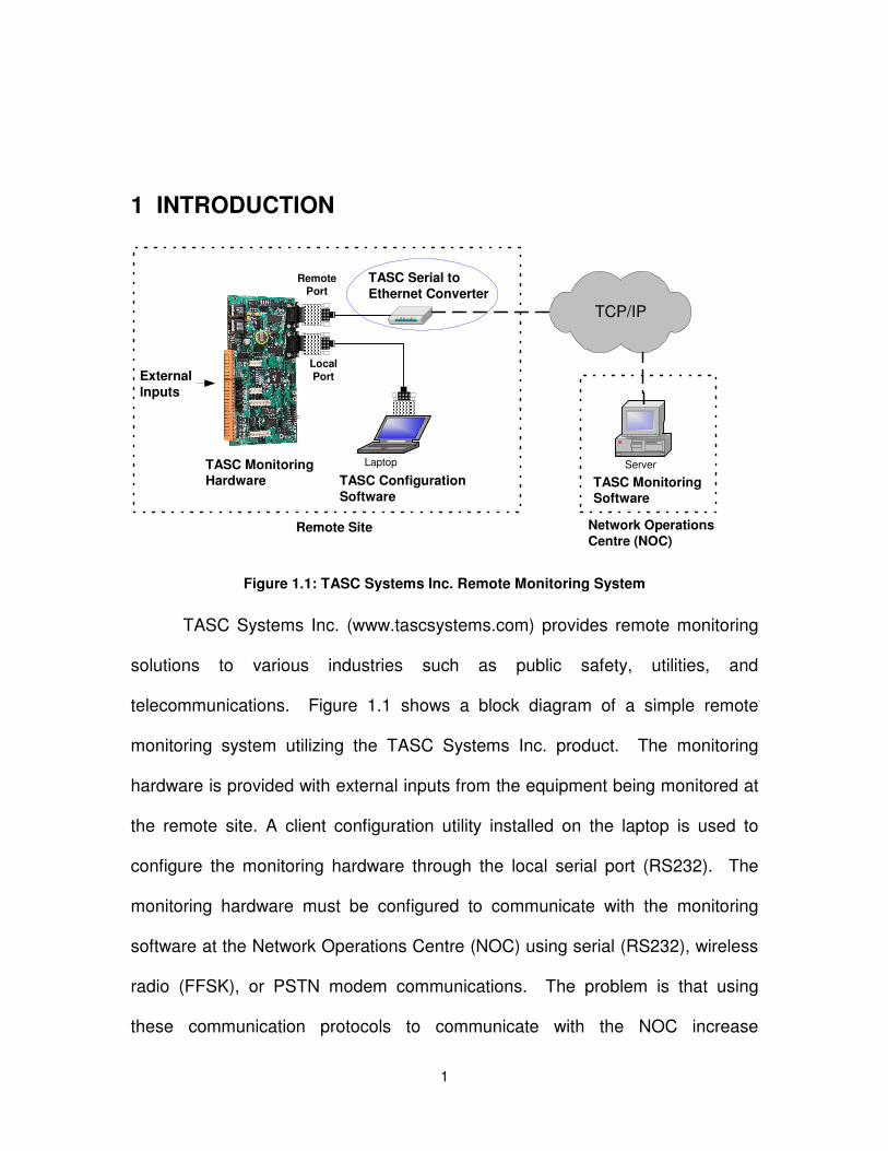
Figure 1.1: TASC Systems Inc. Remote Monitoring System
TASC Systems Inc. (www.tascsystems.com) provides remote monitoring
solutions to various industries such as public safety, utilities, and
telecommunications. Figure 1.1 shows a block diagram of a simple remote
monitoring system utilizing the TASC Systems Inc. product. The monitoring
hardware is provided with external inputs from the equipment being monitored at
the remote site. A client configuration utility installed on the laptop is used to
configure the monitoring hardware through the local serial port (RS232). The
monitoring hardware must be configured to communicate with the monitoring
software at the Network Operations Centre (NOC) using serial (RS232), wireless
radio (FFSK), or PSTN modem communications. The problem is that using
these communication protocols to communicate with the NOC increase

2
communication latencies and decrease throughput. Therefore, Transmission
Control Protocol/Internet Protocol (TCP/IP) communication is required; however,
it is currently only available with the purchase of a proprietary device (available
from multiple manufacturers). The motivation for this project is that the costs
associated with using a proprietary solution are significant, causing TASC
Systems Inc. to investigate designing its own Serial-to-Ethernet Converter (SEC).
The objective is to design a SEC that accepts TCP/IP connections from the
TASC Systems Inc. monitoring software at the NOC and redirects the data over
the serial port to the remote monitoring hardware and vice versa. When utilizing
the SEC, the remote monitoring hardware is configured to communicate serially
(RS232) and is not aware that it is connected to the SEC. The SEC is
transparent as the remote monitoring hardware has no knowledge of the SEC
and thinks it is communicating serially with the monitoring software at the NOC.
On the other end, the monitoring software is configured to talk to the monitoring
hardware using a TCP/IP interface and therefore requires knowledge of the SEC.
The SEC is designed using Xilinx’s MicroBlaze Spartan-3A DSP 1800A
Embedded Development Kit (EDK). The kit consists of the Spartan-3A DSP
1800A Field Programmable Gate Array (FPGA) development board along with
Xilinx’s EDK software. The SEC’s hardware and software are designed using
Xilinx’s EDK software and incorporate the open source lwIP TCP/IP stack along
with Xilinx’s Xilkernel multithreaded kernel. Custom software drivers were also
created and used along with the drivers provided by Xilinx.

3
This report is organized as follows. Chapter 2 describes the hardware and
Chapter 3 the software. Chapter 4 describes the final system’s operation and
verification and Chapter 5 concludes the report and presents opportunities for
future work.

4
2 HARDWARE DESIGN
This chapter describes the hardware system designed for the SEC. The
implementation platform used is the Xilinx MicroBlaze Spartan-3A DSP 1800A
Embedded Development Board. It utilizes the Xilinx Spartan XC3SD1800A-
4FG676 FPGA and includes a 125 Megahertz (MHz) System Clock, an RS232
serial port, 8 Dual Inline Package (DIP) switches, 8 Light Emitting Diodes (LED),
a Joint Test Action Group (JTAG) connector, a 10/100/1000 Ethernet port, a 64
Megabit (Mb) SPI flash, and 128 MegaBytes (MB) of Double Data Rate Two
(DDR2) Synchronous Dynamic Random Access Memory (SDRAM). The
hardware design is implemented on the development board as a prototype for
the final design.
Figure 2.1: Xilinx MicroBlaze Spartan-3A DSP 1800A Development Board

5
2.1 System Description
MicroBlazeProcessor
Data Memory
Dual-Port BlockMemory(32KB)
IntstructionMemory
Local MemoryBus Controller
Local MemoryBus Controller ILMB
DLMB
IPLB
DPLB
MPMC
DXCL
IXCL
SPI Flash Ctlr
Ethernet MAC
Timer
InterruptController
UART
MDMDBG
DDR2 (128 MB)
Flash (64 Mb)
Ethernet PHY
RS232
JTAG
125MHz ClockDCM
125MHz
125MHz_90
62.5MHz
Reset SwitchPSR MODULE
GPIO
GPIO
8 LEDS
8 SWITCHES
FPGA On-Board
TASC MonitoringServer
TASC MonitoringHardware
Host PC forDebugging
External
Figure 2.2: Hardware System
Figure 2.2 shows the components that make up all the hardware required
to design the SEC. The hardware design is implemented on the FPGA using
Xilinx’s EDK with no custom cores. The on-board memory is 128 MB DDR2
SDRAM of which the design requires 1.2 MB and the entire 64 Mb of serial flash
memory. An Ethernet transceiver (PHY) is used to connect the SEC to the TASC
Systems Inc. monitoring software via an Ethernet network. A RS232 transceiver
is used to connect the SEC to the TASC Systems Inc. monitoring hardware. The
eight LEDs and DIP switches are only used for hardware debugging purposes

6
and the JTAG connector is used for connecting to a host Personal Computer
(PC) for software debugging.
2.1.1 MicroBlaze Processor
Figure 2.3: MicroBlaze Block Diagram [4]
The MicroBlaze is a soft 32-bit RISC Harvard architecture processor with
32 32-bit general purpose registers, an Arithmetic Logic Unit (ALU), and many
other optional features as shown in Figure 2.3 [4]. The optional features used in
this design are the barrel shifter, integer multiplier, and pattern comparator to
improve software performance. The barrel shifter executes any shifting
instructions in two cycles and the hardware multiplier executes any integer
multiplication in 3 cycles. The pattern comparator (not shown in Figure 2.3)
enhances any compare instructions by completing a byte-wise comparison with a
32 bit word in one cycle. The processor is implemented using a three-stage

7
pipeline instead of five to conserve area, as the additional performance is not
required. A system clock frequency of 62.5MHz is used as it is a multiple of the
125 MHz clock used for the DDR2 memory. Instruction and data caching are
utilized in this design; an 8 KB instruction cache and 4 KB data cache meet the
design requirements when used in conjunction with 32KB of shared BRAM for
the local data memory (2KB) and local instruction memory (11KB). The cache is
created using Block RAM (BRAM) (see section 2.1.6) and interfaces with
MicroBlaze via the CacheLink (XCL) busses. For more details, [4] may be
referenced.
2.1.2 Processor Local Bus (PLB) v4.6
The Xilinx Processor Local Bus (PLB) v4.6 is used by MicroBlaze to
connect to all the peripherals in the system. It has separate address, data, and
control paths. This design uses 32 bits for the address bus and 64 bits for the
data bus. For more details, [6] may be referenced.
2.1.3 Multi-Port Memory Controller (MPMC) and DDR2 Memory
The Multi-Port Memory Controller (MPMC) provides an interface between
the DDR2 memory and the CacheLink (XCL) and PLB busses. The MPMC has
eight input ports that can be used by various peripherals to access the DDR2
memory. In the current design, three ports are used: the PLB, the Data
CacheLink (DXCL), and the Instruction CacheLink (IXCL). 1.2 MB of DDR2
SDRAM memory is used to store the main software, which is comprised of the

8
code and data sections (see section 3.1). For more details, [8] may be
referenced.
2.1.4 XPS SPI Interface and Serial Flash Memory
The Xilinx Platform Studio (XPS) Serial Peripheral Interface (SPI) provides
an interface between the MicroBlaze processor (using the PLB bus) and the
64Mb Intel S33 serial flash memory. The optional sixteen byte transmit and
receive buffers are utilized to minimize the impact on system performance. The
system boots from the serial flash memory and thus the FPGA bitstream, the
boot-loader software, and the main software are stored in the serial flash
memory. For more details, [16] may be referenced.
2.1.5 XPS Ethernet Lite Media Access Controller (EMAC)
The XPS Ethernet Lite MAC (EMAC) provides an interface between the
Physical Layer (PHY) device using the IEEE Std. 802.3 Media Independent
Interface (MII) and MicroBlaze via the PLB interface. The EMAC can operate at
10 Megabits per second (Mbps) or 100 Mbps. It has 2 KB transmit and receive
buffers (ping buffers) for holding data for a single Ethernet packet and optional 2
KB transmit and receive buffers (pong buffers) to provide ping-pong buffering.
Ping-Pong buffering is utilized in the current design to provide maximum
throughput. The core also provides transmit and receive interrupts that are
utilized by the software. For more details, [13] may be referenced.
9
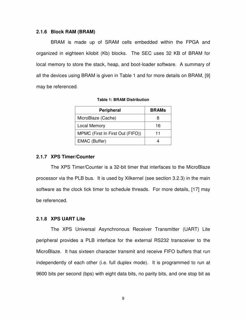
2.1.6 Block RAM (BRAM)
BRAM is made up of SRAM cells embedded within the FPGA and
organized in eighteen kilobit (Kb) blocks. The SEC uses 32 KB of BRAM for
local memory to store the stack, heap, and boot-loader software. A summary of
all the devices using BRAM is given in Table 1 and for more details on BRAM, [9]
may be referenced.
Table 1: BRAM Distribution
Peripheral BRAMs
MicroBlaze (Cache) 8
Local Memory 16
MPMC (First In First Out (FIFO)) 11
EMAC (Buffer) 4
2.1.7 XPS Timer/Counter
The XPS Timer/Counter is a 32-bit timer that interfaces to the MicroBlaze
processor via the PLB bus. It is used by Xilkernel (see section 3.2.3) in the main
software as the clock tick timer to schedule threads. For more details, [17] may
be referenced.
2.1.8 XPS UART Lite
The XPS Universal Asynchronous Receiver Transmitter (UART) Lite
peripheral provides a PLB interface for the external RS232 transceiver to the
MicroBlaze. It has sixteen character transmit and receive FIFO buffers that run
independently of each other (i.e. full duplex mode). It is programmed to run at
9600 bits per second (bps) with eight data bits, no parity bits, and one stop bit as

10
those are the parameters used by the TASC Systems Inc. monitoring hardware.
For more details, [18] may be referenced.
2.1.9 XPS Interrupt Controller (INTC)
The XPS Interrupt Controller (INTC) takes up to 32 interrupts from various
peripheral devices and produces a single output. The INTC is required in this
design because the MicroBlaze processor has only one interrupt input and there
are three interrupt generating peripherals (EMAC, Timer, and UART). Priority
structure of the interrupts in this system is (highest to lowest): Timer, EMAC, and
UART. The timer is given the highest priority as it is the reference for all the
software timers and the kernel’s scheduler. The EMAC is next as it can only
buffer two Ethernet packets and the Ethernet link is faster than the UART link.
Finally, the UART is given the lowest priority as it runs significantly slower than
the rest of the system. For more details, [15] may be referenced.
2.1.10 XPS General Purpose Input/Output (GPIO)
Two XPS General Purpose Input/Output (GPIO) modules are used for the
LED’s and DIP switches. The modules provide an interface between the
MicroBlaze processor (via the PLB Bus) and the LEDs and DIP switches. They
are configured to use 8 bits as that corresponds to the number of LEDs and
switches available on the board. For more details, [14] may be referenced.

11
2.1.11 MicroBlaze Debug Module (MDM)
The MicroBlaze Debug Module connects to the host PC for software
debugging via a JTAG interface. It connects to the MicroBlaze processor using
the debug bus. For more details, [10] may be referenced.
2.1.12 Clock Generator
The Clock Generator module provides the clocks required by the system
by automatically instantiating Digital Clock Manager (DCM) modules. The board
used for the prototype has a 125 MHz oscillator that is used to generate the three
clocks required by the current design: 125 MHz, 125 MHz with a 90 degree
phase shift (125MHz_90), and 62.5 MHz. The DDR2 MPMC uses the 125 MHz
and 125MHz_90 clocks and the MicroBlaze and all the other peripherals use the
62.5 MHz clock. For more details, [11] may be referenced.
2.1.13 Processor System Reset (PSR) Module
The Processor System Reset (PSR) module allows the sequencing of
reset signals to different peripherals. After a reset, the first thing to come up is
the PLB bus followed by the peripherals (sixteen clocks delay) and lastly,
MicroBlaze (sixteen clocks delay). For more details, [12] may be referenced.

12
2.2 System Resource Utilization
Tables 2 summarizes the resource requirements of the entire hardware
design and the percent utilization of the FPGA.
Table 2: Hardware Resource Utilization
Resource Type Used % of
XC3SD1800A
Flip Flops 4881 14
4 Input LUTs 5801 17
IOBs 110 21
BRAMs 39 46

13
3 SOFTWARE DESIGN
This section will describe the design of the software for the SEC. In the
design of the SEC, the software is divided into two parts: the boot-loader
software and main software. The boot-loader software has the responsibility of
loading and starting the main software. The main software has the primary
function of accepting TCP/IP connections from the TASC Systems Inc.
monitoring software and redirecting the data over the serial port to the remote
monitoring hardware and vice versa.
3.1 System Description
Figure 3.1 shows the layers of the SEC system architecture with the first
layer being the implementation platform and the second layer containing the
hardware design. The Board Support Package and the low-level and high-level
drivers make up the third layer. The Board Support Package (BSP) is used to
access processor specific functions such as interrupt handling, instruction and
data cache handling, and exception handling. Xilinx’s low-level drivers act as a
direct interface to the hardware and are typically implemented using macros and
manifest constants. The high-level drivers or device drivers, provided by Xilinx
and designed as part of this project provide abstraction from hardware changes.
The fourth and fifth layers contain the kernel (Xilkernel) and the TCP/IP stack
(lwIP) respectively. The Xilkernel is a small, robust, modular, and free kernel,

14
which makes it a great choice for memory-and cost-constrained applications
such as this one. “lightweight IP” (lwIP) is an open source (Berkeley Software
Distribution (BSD) license) TCP/IP stack designed for embedded systems. The
last layer is made up of two applications: “main” and “boot-loader”. The main
software is comprised of layers three to five and the “main” application of layer
six. The boot-loader software is comprised of layer three and the “boot-loader”
application of layer six. The SEC software is comprised of the main and boot-
loader software.
Drivers (Low Level)
BSP
Xilkernel
lwIP
Hardware Design
Drivers(High Level)
Application(Boot-loader, Main)
Implementation Platform
Software
Figure 3.1: Serial-to-Ethernet Software Layered Architecture
3.2 System Components
3.2.1 Board Support Package (BSP)
The BSP is used to access processor specific functions such as interrupt
handling, instruction and data cache handling, and exception handling. It is
generated by the EDK software using the Library Generator (Libgen) utility

15
provided by Xilinx. Along with the low-level drivers, it makes up the lowest layer
of software modules.
3.2.2 Drivers
Xilinx’s low and high-level drivers are used as well as a custom SPI serial
flash driver and UART interrupt handler.
3.2.2.1 Xilinx’s Low-level Drivers
Xilinx’s low-level drivers use macros and manifest constants to allow a
developer to create small applications or custom high-level drivers. They
typically have the following characteristics:
• Constants that define registers offsets and bit fields, and simple macros to access hardware registers
• Small memory footprint
• Little to no error checking
• Minimal abstraction
• Polled I/O operation only
The UART and SPI controller low-level drivers are utilized in the software
as they are more efficient than the high-level drivers.
3.2.2.2 Xilinx’s High-level Drivers
The high-level drivers or device drivers provide abstraction from hardware
changes. They are implemented with macros and functions and designed to
allow the developer to take advantage of all the features of the hardware. They
are built partly upon the low-level drivers and are independent of operating

16
systems and processors making them highly portable. They typically have the
following characteristics:
• An abstract interface isolates developer from hardware changes
• Error checking
• Polled and interrupt driven I/O
• Larger memory footprint
Xilinx’s high-level drivers are used for all of the peripherals except for the
UART and SPI controller.
3.2.2.3 Custom SPI Serial Flash Driver
A custom SPI master serial flash driver is used to alleviate the complexity
and size of Xilinx’s driver for interfacing to the Intel S33 serial flash. The driver
needs to be small and efficient to prevent extensive memory usage and long boot
up delays as it is used in the boot-loader software. The SPI controller is to
operate as a master and therefore, the driver is written only for an SPI master
interface to the serial flash. The driver is built upon Xilinx’s SPI controller low-
level driver and consists of three functions: flash_read_start, flash_read_stop,
and flash_rw_data. The driver currently provides the ability to only read from the
serial flash as writing capability will be added in the future if required.
3.2.2.3.1 flash_rw_data Function
The flash_rw_data function reads and writes data to the SPI Intel S33
serial flash. The inputs to the function are two buffers, rxdata and txdata, and a
counter rw_bytes. The buffers store the data to be received and transmitted and
the counter determines the number of bytes to be transmitted and received. In

17
the SPI protocol, for every byte sent, a byte is received. Thus, in order to read
data from the serial flash, a known string of bytes is sent to the flash and the data
requested is received by the SPI controller. Referring to Figure 3.2, a check is
done to see if the rw_bytes counter is zero. If the rw_bytes counter is not zero, a
byte is sent to the flash and then a byte is received from the flash. The rw_bytes
counter is then decremented and the loop continues until all the bytes have been
transmitted and received from the flash. Next, the data in the receive buffer of
the SPI controller is transferred to the rxdata buffer.
rw_bytes=0?NO Send txdata Byte to
Flash
End
Start
YES Decrement rw_bytes
SPI Rx BufferEmpty?
NO Read Byte into rxdataBuffer
YES
Figure 3.2: flash_rw_data Function Flowchart
3.2.2.3.2 flash_read_start and flash_read_stop Functions
The flash_read_start function initializes the serial flash to start transmitting
data from a specified serial flash sector. The inputs to the function are the base
address of the SPI controller and the flash sector address. Figure 3.3 shows the
flowchart of the flash_read_start function. The function starts off by enabling the
SPI controller and selects the serial flash. The sector address is then set in the

18
txdata buffer and sent to the flash_rw_data function for transmitting the read
command.
Enable SPI Controller &Select Flash
Set Sector Address
Send Read Command toFlash
Start
End
Figure 3.3: flash_read_start Function Flowchart
The flash_read_stop function is very simple as it takes in the base
address of the SPI controller and disables the SPI controller and de-selects the
flash.
3.2.2.4 Custom Uart Interrupt Handler
A custom UART handler was developed as Xilinx’s interrupt handler has a
lot of overhead. The custom handler is very simple as required and utilizes
Xilinx’s UART low-level driver. The UART generates an interrupt when it finishes
transmitting data or when it receives data. In the software, it is used only to
buffer the receive data. Referring to Figure 3.4, the handler checks to see if the
interrupt is a receive event and if it is, it stores the data in the buffer.

19
Start
Rx Event?
Buffer UART RX Data
End
NO
YES
Figure 3.4: UART Interrupt Handler
3.2.3 Xilkernel
Xilkernel is an embedded processor kernel that can be tailored to a great
extent for different embedded system applications. It has the key features of
embedded kernels such as multi-tasking, priority-driven pre-emptive scheduling,
inter-process communication, synchronization facilities, and interrupt handling.
Xilkernel is small (~22KB), robust, modular, and free, which makes it a great
choice for memory and cost constrained applications.
3.2.4 lightweight IP (lwIP)
lightweight IP (lwIP) is an open source (BSD license) TCP/IP stack
designed for embedded systems. lwIP provides both a RAW interface and a
BSD sockets style interface to the TCP/IP stack. The BSD sockets interface is
used in the design of the SEC as it provides a well known standard interface.
lwIP supports the following protocols:
• Internet Protocol (IP)
• Internet Control Message Protocol (ICMP)
• User Datagram Protocol (UDP)

20
• Transmission Control Protocol (TCP)
• Address Resolution Protocol (ARP)
• Dynamic Host Configuration Protocol (DHCP)
3.3 Boot-loader Software
The boot-loader software reads the main software and MicroBlaze vectors
from the flash memory and stores them in DDR2 RAM and BRAM respectively.
Once that is complete, the “main” application is started as shown in Figure 3.5.
3.3.1 Description
Referring to Figure 3.5, the “boot-loader” application starts off by
initializing and enabling the data and instruction cache. Initialization of the data
and instruction cache requires invalidating the entire cache memories. Enabling
the cache sets up MicroBlaze to start using the cache. Next the SPI controller is
initialized by making sure it is set up to operate as a master and the slave select
is set to select nothing. The SPI controller is then enabled making it ready to
start sending/receiving data. The serial flash is organized into 64 KB sectors and
the main application software stored at sector 17 and on. The read command
tells the serial flash to go into read mode and start reading from the specified
address (i.e. sector 17).

21
Initialize & Enable Cache
Initialize SPI Controller
Enable SPI Controller
Read Main Application Data
and Store in DDR2 RAM
Verified 1000Bytes?
NO
YES
Enable Flash Read fromMain Application Sector
Read Vectors Data and Storein Block RAM
VerifiedVectors?
YES
Enable Flash Read fromVectors Sector
NO
Disable Flash Read
Disable Flash Read
Print Main App Error
Print Vector Error
Start Main Application
Enable Flash Read fromMain Application Sector
Disable Flash Read
Enable Flash Read fromVectors Sector
Disable Flash Read
End
Start
Figure 3.5: “Boot-loader” Application Flowchart

22
The main software is then transferred from the flash memory and stored
into the DDR2 memory. Then the flash memory is deselected. To verify the data
was transferred properly, the flash memory is reselected and 1000 bytes are
read and compared with the data in the DDR2 RAM. Only 1000 bytes is used for
verification as it takes longer to verify the entire software. Again after the read,
the flash is deselected.
The MicroBlaze vectors are the next set of data that get transferred. The
vectors need to be loaded into BRAM from address 0x00 to 0x50. The next steps
are the same as with the loading the main software data except that the vectors
are stored in BRAM and sector 50 of the flash is used to retrieve the data. Once
that is complete, the “main” application is launched.
3.4 Main Software
The main software has the primary function of accepting TCP/IP
connections from the TASC Systems Inc. monitoring software and redirecting the
data over the serial port to the remote monitoring hardware and vice versa.
Table 3 outlines the threads used in the main software.

23
Table 3: Main Software Threads
Thread Creator Active Function
main_thread Main Temporary First thread called after Xilkernel initialization. Used to initialize lwIP (spawns tcpip_thread), and the network interface. Spawns xemacif_input_thread and main_application_thread.
tcpip_thread Main Always Processes TCP/IP packets. Provided by lwIP.
xemacif_input_thread Main Always Recieves data processed by the EMAC interrupt handlers and passes it to the tcpip_thread. Provided by Xilinx.
main_application_thread Main Always Waits for a connection request and spawns the se_thread
se_thread Main Temporary Spawned by the main_application_thread. Performs the function of converting serial data to Ethernet and vice versa.
Idle Xilkernel Temporary Is run if there are no other threads ready to run. Provided by Xilinx.
3.4.1 Initialization Description
Initialize & Enable Cache
Start
Initialize Xilkernel
End
Figure 3.6: “Main” Application Initialization Flowchart

24
Referring to Figure 3.6, the “main” application starts off by initializing and
enabling the data and instruction cache. Initialization of the data and instruction
cache requires invalidating the entire cache memories. Enabling the cache sets
up the MicroBlaze to start using the cache. Xilkernel is then initialized and
started, which involves starting the kernel, enabling interrupts, and starting the
main_thread thread. All threads in the system have the same priority as per the
recommendation on page 167 of [1] and thus Xilkernel is using a round robin
scheduling policy.
Initialize lwIP
Initialize Network Interface
Start xemacif_input_thread
Startmain_application_thread
End
Start
Figure 3.7: main_thread Thread Flowchart
Referring to Figure 3.7, the main_thread thread starts off by initializing the
lwIP TCP/IP stack, which involves initializing data structures for the stats,
system, memory, pbufs, ARP, IP, UDP, and TCP layers. The tcpip_thread
thread (provided by lwIP) is also spawned in the lwIP initialization. Initializing the
network interface is done by providing the IP address, network mask, gateway IP
address, EMAC address, and the base address of the XPS Ethernet Lite core to

25
lwIP. The initialized network interface is set to be the default interface (in our
case we only have one) to be used by lwIP. Once lwIP has been notified that the
network interface is ready, Xilinx’s EMAC input thread (xemacif_input_thread) is
started. This thread receives data processed by the EMAC interrupt handlers,
and passes it to the lwIP tcpip_thread thread. Once that is complete, the
main_application_thread thread is started.
3.4.2 main_application_thread Thread Flowchart Description
Referring to Figure 3.8, the main_application_thread uses the BSD
sockets interface provided by lwIP. First a TCP socket is created to provide an
endpoint for communication and then bound to a port number. The “listen”
function call then turns the socket into a listening socket that can accept
incoming connections. The UART interrupt handler is then registered with
Xilkernel as it processes all the interrupts from the interrupt controller. Before
UART interrupts are enabled, the UART Rx circular buffer structure is initialized
with the correct length and location of the global buffer. Now the UART core
interrupt and the UART interrupt in the interrupt controller are enabled so the
UART interrupt handler may begin buffering data. A call is made to the BSD
sockets “accept“ function, which blocks until a connection request is made. Once
a connection request has been made, the connection is accepted and a check to
see if there is a Serial-to-Ethernet session in progress is made. If there is a
Serial-to-Ethernet session in progress, the socket is closed as we can only have
one Serial-to-Ethernet session currently. If there is no Serial-to-Ethernet session
in progress, a new Serial-to-Ethernet thread is created to handle the request and

26
the Session In Progress flag is set to true. The main_application_thread goes
back to waiting for new connection requests.
Create TCP Socket
Bind Socket to Port
Set Socket to Listen
Register UART InterruptHandler
Initialize UART Rx CircularBuffer
Enable UART Interrupt
ConnectionRequest?
NO
Create Serial to EthernetThread
YES
Session InProgress?
NO
YESClose New Socket
Start
Session In Progress=True
Figure 3.8: main_application_thread Flowchart

27
3.4.3 se_thread Thread Description
Read Password
Decrement Activity Timer
PasswordCorrect?
NO
Any IP RXData?
NO
YES
Make IP Read NON Blocking
Any UARTRX Data?
YES
NO
Activity TimerExpired?
YES
NO
Close Socket
Session In Progress = False
Send to UART &Reset Activity Timer
Send IP & ResetActivity Timer
Connected?NO
YES
Reset Activity Timer
End
Start
Init
YES
Yield
Figure 3.9: se_thread Thread Flowchart

28
When a Serial-to-Ethernet thread (se_thread) is spawned, the activity
timer and counters are initialized. A password authentication process is then
started to validate the device trying to connect is allowed to communicate with
the TASC Systems Inc. monitoring hardware. If the password is incorrect, the
socket is closed, the Session In Progress flag (Fig 3.9) is set to false, and the
thread is destroyed. If the authentication is successful, the BSD sockets read
function is set to non-blocking and a check for data received over the TCP/IP link
is done. If valid data has been received, the activity timer is reset signifying that
there is activity on the link, and the data is sent to the TASC Systems Inc.
hardware via the UART. When the data has been sent or if there was no valid
data received, a check is done to see if there is valid data received in the UART
receive buffer. If valid data has been received, the activity timer is reset
signifying that there is activity on the link, and the data is sent to the TASC
Systems Inc. software over the TCP/IP link. To determine when to send the data
received from the UART, a timer of sixteen milliseconds is used. Once the last
byte has been received, the SEC waits sixteen milliseconds before the data is
sent to make sure there is no more data to be sent. This additional time is
compensated for in the TASC Systems Inc. protocol by increasing the timing
windows. When the data has been sent or if there was no valid data received, a
check is done to see if the fifteen second activity timer has expired. If the activity
timer hasn’t expired, the timer is decremented and the thread yields the
processor to another thread. If the activity timer has expired, a check is done to
see if the connection is still up by sending data to the TASC Systems Inc.

29
software. If it is, the activity timer is reset and the thread yields the processor to
another thread. If there is no response, the socket is closed, the Session In
Progress flag is set to false, and the thread is destroyed.
Currently the se_thread thread is a polling thread and in order to make it a
non-polling thread a couple of things would need to be changed. The thread
would need to be split into two threads: uart_to_ip and ip_to_uart. The uart_to_ip
thread would send the data received by the UART over the TCP/IP link. It would
wait on a semaphore from the UART interrupt handler which would be posted
when data is received on the serial port. The ip_to_uart thread would block on
the BSD sockets read function and wait for TCP/IP data to be received. Once
valid data has been received, it would transmit the data over the serial link.
In order to port this software into a larger system, the se_thread would
most likely have to be split up per the proposed non-polling method. As of right
now, the polling thread is always either ready-to-run or running and therefore can
delay other threads from being scheduled on the processor when useful work
arrives for them to do. In order to increase the efficiency of the software, the yield
primitive is utilized to quickly release the processor when there is no useful work
waiting for the se_thread to do. This implementation is sufficient for the current
product as there are a limited number of threads but for larger systems, further
degradation in performance may be observed.

30
4 SYSTEM DESIGN AND PERFORMANCE
4.1 Boot-loading the Hardware Design
In order to have the Spartan 3A DSP FPGA operate as a SEC on power
up, it must program itself from the SPI serial flash. The Spartan 3A DSP FPGA
board has a built-in SPI interface to communicate with the serial flash and using
the MODE pins, it is set to program itself from the serial flash.
The serial flash must be programmed with the appropriate bitstream in
order for the FPGA to program itself. A bitstream is made up of programming
bits and can be directly loaded onto the FPGA via JTAG using Xilinx’s iMPACT
software. If we want to store this bitstream on the serial flash, we must convert it
into MCS format using the iMPACT software. The Xilinx EDK software integrates
the boot-loader application into the MicroBlaze’s Local BRAM bitstream using
Xilinx’s DATA2MEM utility. The main software is in the executable and linkable
format (ELF) and must be converted to MCS format. Since the MicroBlaze
Interrupt Vector Table (IVT) needs to be stored in BRAM and the main software
needs to be stored in DDR2 SDRAM, the ELF file must first be separated into
two binary files (app.b, vectors.b). Once separated, Xilinx’s xmcsutil utility
software is used to convert the binary files to MCS format. The three files
(app.mcs, vectors.mcs, bitstream.mcs) then are combined into a single file
(combined.mcs) by xmcsutil. Using the combined.mcs file, the serial flash is then
programmed with Xilinx’s xip utility software.

31
In the creation of the combined.mcs file, an offset has to be specified for
each of the MCS files that defines the location of the individual files in the
combined file. In order to determine the offsets, an understanding of the size of
each file is required. The bitstream is 1024660 (0xFA294) bytes in size and is
placed at the starting of the serial flash (Figure 4.1). The main software’s size is
1167724 (0x11D16C) bytes and is started at sector 17. The MicroBlaze vectors
size can be a maximum of 80 (0x50) bytes and is started at sector 50, providing
room for the main software to grow in the future. The remaining memory of the
serial flash can be used for non volatile storage.
0x110000 (Sector 17)
Bitstream
0x320000 (Sector 50)
Main Software
MicroBlaze IVT
0x000000 (Sector 0)
0x800000
Figure 4.1: Serial Flash Memory Map

32
4.2 System Performance
4.2.1 TCP Throughput
The TCP throughput was not tested but is documented on pg 174 of [1].
The maximum TCP throughput is 7 Mbps in socket mode on any Spartan 3
FPGA with MicroBlaze and the Ethernet Lite core using a system frequency of 66
MHz [1]. This design uses a system frequency of 62.5 MHz, which may have
reduced the throughput below 7 Mbps, but the existing throughput is sufficient for
the purpose of the current design.
4.2.2 Comparison of Local and Serial-to-Ethernet Connections
LocalPort
Laptop
Local Connection
TASC Monitoring
Hardware TASC Configuration
Software
LocalPort
LaptopTASC Monitoring
Hardware
TASC Serial to
Ethernet Converter
TASC Configuration
Software
Ethernet Crossover
Cable (6 ft)
Serial Cable
(6 ft)
Serial
Cable
(6 ft)
Serial-to-Ethernet Connection
Figure 4.2: Test Setup
Testing was also performed on the TASC Systems Inc. remote monitoring
system. Referring to Figure 4.2, the local connection uses a standard serial
cable to connect the hardware to the computer and this is the baseline as it is the
fastest connection. The SEC is connected to the TASC Systems Inc. hardware
using a null-modem serial cable and connected directly to the computer using an

33
Table 4: Completion Time of Typical Commands
Test Function SEC Time
(ms)
Local Time (ms)
SEC Latency
(ms)
Number of
Packets
Number of
Bytes
Proprietary Device
Time (ms)
Read Contact Status 290 90 200 2 22 251
Read Temperature Status 310 97 213 2 32 273
Read Analog Status 320 100 220 2 36 281
Table 5: Network Protocol Analyzer Output of Read Contact Status Function
Time (millisecond) Source Destination
TCP Packet Type
Data Length
0 Monitoring Software Serial-to-Ethernet Data 8
39 Serial-to-Ethernet Monitoring Software ACK 0
136 Serial-to-Ethernet Monitoring Software Data 14
290 Monitoring Software Serial-to-Ethernet ACK 0
Ethernet crossover cable. Table 4 summarizes the time required for completion
of some typical commands used in the TASC Systems Inc. remote monitoring
system. Three test functions were executed: Read Contact Status, Read
Temperature Status, and Read Analog Status. The Listen32 serial line data
monitor and the Wireshark network protocol analyzer were installed on the laptop
computer shown in Figure 4.2 and used to determine the timing results for the
local, SEC, and the proprietary device connections. The latency is determined
by taking the difference between the local time and the SEC time. The total
number of bytes transferred and the number of packets used is shown as well.
By averaging the SEC latency, it can be seen that it takes approximately
211 milliseconds (ms) longer on average to perform the functions using the SEC.
The proprietary device completion times are shown as well with it requiring an
additional 173 ms (average of proprietary device latency) on average to perform
the functions. Table 5 shows a network protocol analyzer output that breaks

34
down the time required to perform a read contact status function. It can be seen
that initially the monitoring software sends a request data packet to the
monitoring hardware. The TCP packet is then acknowledged by the SEC 39 ms
later and 97 ms after that, the monitoring hardware’s response is received. 154
ms later, the monitoring software sends a TCP acknowledgement to the SEC.
From Table 5, the latency of the SEC for the read contact status function is 136
ms minus the baseline of 90 ms from Table 4 which gives a latency of 46 ms.
Further investigation is required to determine why the monitoring software takes
154 ms to acknowledge the response as this increases the Serial-to-Ethernet
solution latency to approximately 200 ms. Even with the additional latency from
the monitoring software, the results are well within the requirements of TASC
Systems Inc.

35
5 CONCLUSION
TASC Systems Inc. (www.tascsystems.com) provides remote monitoring
solutions that require TCP/IP connectivity. Currently a proprietary device is used
to accomplish this functionality but the costs associated with using a proprietary
solution have resulted in TASC Systems Inc. wanting to investigate the design of
its own SEC.
The implementation platform used is the Xilinx MicroBlaze Spartan-3A
DSP 1800A Embedded Development Board. The hardware design is
implemented on the development board as a prototype for the final design. The
core of the hardware logic design is the MicroBlaze processor, which is
connected to the following peripherals: MPMC, SPI controller, EMAC, timer,
UART Lite, LED and DIP switch GPIO, and an interrupt controller. The design
uses 32 KB of local BRAM memory and the external memory is composed of 128
MB DDR2 SDRAM of which the design requires 1.2MB to store the main
software. A 64 Mb serial flash is used to store the hardware design bitstream
along with the software.
A six layer architecture is used in the Serial-to-Ethernet design with the
first and second layers being the implementation platform and hardware design
respectively. The third layer contains the Board Support Package (BSP) and the
high and low-level drivers. The fourth and fifth layers contain the kernel
(Xilkernel) and the TCP/IP stack (lwIP) respectively. The last layer is made up of

36
the main and boot-loader applications. The boot-loader software has the
responsibility of loading and starting the main software. The main software has
the primary function of accepting TCP/IP connections from the TASC Systems
Inc. monitoring software and redirecting the data over the serial port to the
remote monitoring hardware and vice versa.
Performance testing was completed by sending typical commands over
the Serial-to-Ethernet link and comparing the results with a local serial link. The
results showed that the Serial-to-Ethernet latency was well within TASC Systems
Inc. requirements.
The testing showed that there may be an issue with TASC Systems Inc.
configuration software as it takes 154 ms to acknowledge a read contact status
response. In the future, further investigation into the effect of varying cache sizes
on performance may be investigated along with changing the kernel’s scheduling
policy to pre-emptive and adjusting thread priorities. In order to make the SEC
software more scalable, the proposed modification of the se_thread with the use
of semaphores would be required.

37
REFERENCES
[1] Xilinx (July 30, 2008). OS and Libraries Document Collection. [Online]. Available:
http://www.xilinx.com/support/documentation/sw_manuals/edk10_oslib_rm.pdf
[2] Xilinx (September 18, 2008). EDK Concepts, Tools, and Techniques. [Online]. Available:
http://www.xilinx.com/support/documentation/sw_manuals/edk_ctt.pdf
[3] Xilinx (2008). Embedded Systems Tools Reference Manual. [Online]. Available:
http://www.xilinx.com/support/documentation/sw_manuals/edk10_est_rm.pdf
[4] Xilinx (July 14, 2008). MicroBlaze Processor Reference Guide UG081 (v9.3).
[5] Xilinx (July 28, 2008). Local Memory Bus (LMB) V1.0 (v1.00a).
[6] Xilinx (July 28, 2008). Processor Local Bus (PLB) v4.6 (v1.03a).
[7] Xilinx (July 28, 2008). LMB BRAM Interface Controller (v2.10a).
[8] Xilinx (September 26, 2007). Multi-Port Memory Controller (MPMC) (v3.00a).
[9] Xilinx (March 12, 2007). Block RAM (BRAM) Block (v1.00a).
[10] Xilinx (June 25, 2008). MicroBlaze Debug module (MDM) (v1.00d).
[11] Xilinx (March 15, 2007). Clock Generator (v1.00a).
[12] Xilinx (July 29, 2008). Processor System Reset Module (v2.00a)
[13] Xilinx (January 14, 2008). XPS Ethernet Lite Media Access Controller (v1.00a).
[14] Xilinx (July 22, 2008). XPS General Purpose Input/Output (GPIO) (v1.00a).
[15] Xilinx (July 22, 2008). XPS Interrupt Controller (v1.00a).
[16] Xilinx (April 17, 2008). XPS Serial Peripheral Interface (SPI) (v1.00a).

38
[17] Xilinx (April 21, 2008). XPS Timer/Counter (v1.00a).
[18] Xilinx (July 18, 2008). XPS UART Lite (v1.00a).
[19] Stang, Pascal. (2006). Proycon AVRlib. [Online]. Available:
http://www.mil.ufl.edu/~chrisarnold/components/microcontrollerBoard/AVR/avrlib/docs/html/index.html
[20] Velusamy, Siva. (April 11, 2008). Lightweight IP (lwIP) Application Examples. [Online]. Available:
http://www.xilinx.com/support/documentation/application_notes/xapp1026.pdf
[21] Fletcher, Bryan. (February 19, 2008). Remote Configuration Update on the Xilinx 3SD1800AP. [Online]. Available:
https://www.em.avnet.com/common/filetree/0,2740,RID%253D%2526CID%253D42106%2526CAT%253D0%2526CCD%253DUSA%2526SID%253D32214%2526DID%253DDF2%2526SRT%253D1%2526LID%253D32232%2526PRT%253D0%2526PVW%253D%2526PNT%253D%2526BID%253DDF2%2526CTP%253DEVK,00.html