serial eeprom - 慧聪网img00.b2b.hc360.com/pic-0/handbook-pic-0/0-0-197540… · ·...
TRANSCRIPT

Spring 2008
SerialEEPROM
K24C128 / K24C256
128K (16,384 X 8) /256K (32,768 X 8)Two-Wire Serial EEPROM
K24C128/K24C256
V 1 . 1V 1 . 1Spring 2008 .001..001.
Low-voltage Operation
- 1.8 (VCC = 1.8V to 5.5V)
Operating Ambient Temperature: -40°C to +85°C
Internally Organized:
- 16,384 X 8 (128K)
- 32,768 X 8 (256K)
Two-wire Serial Interface
Schmitt Trigger, Filtered Inputs for Noise Suppression
Bidirectional Data Transfer Protocol
400 kHz (1.8V, 2.7V, 5V) Compatibility
Write Protect Pin for Hardware Data Protection
64-byte Page (128K/256K) Write Modes
Partial Page Writes Allowed
Self-timed Write Cycle (5 ms max)
High-reliability
- Endurance: 1 Million Write Cycles
- Data Retention: 100 Years
8-lead PDIP, 8-lead JEDEC SOIC and 8-lead
TSSOP Packages
Features
General Description
The K24C128/K24C256 provides 131,072/262,144 bits of serial electrically erasable and programmable read-only
memory (EEPROM) organized as16,384/32,768 words of 8 bits each. The device is optimized for use in many industrial
and commercial applications where low-power and low-voltage operation are essential. The K24C128/K24C256 is
available in space-saving 8-lead PDIP, 8-lead JEDEC SOIC, and 8-lead TSSOP packages and is accessed via a
Two-wire serial interface. In addition, the K24C128/K24C256 is available in 1.8V (1.8V to 5.5V) version.
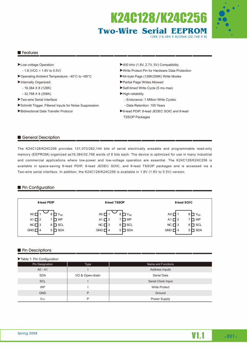
Pin Configuration
Pin Descriptions
Pin Designation
A0 - A1
SDA
SCL
GND
WP
VCC
Name and Functions
Write Protect
Address Inputs
Serial Data
Serial Clock Input
Ground
Power Supply
I
I
I
P
P
Type
Table 1: Pin Configuration
I/O & Open-drain
SDA
SCL
WP
VCC1
2
3
4
8
7
6
5
A0
1
GND SDA
SCL
WP
VCC1
2
3
4
8
7
6
5
A0
A1
GN
8-lead PDIP
SDA
SCL
WP
VCC1
2
3
4
8
7
6
5
A0
A1
GN
8-lead SOIC8-lead TSSOP
A
CN CN CN
D D
Spring 2008 .002.
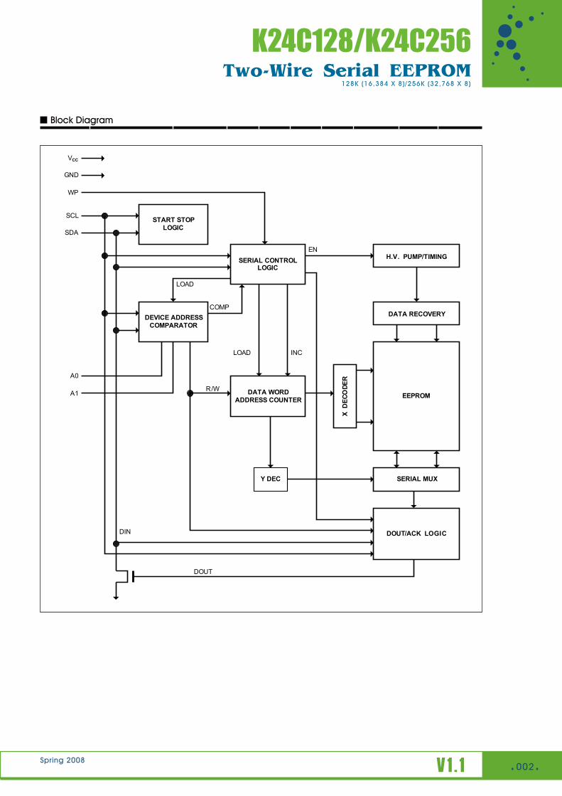
Block Diagram
SDA
SCL
WP
VCC
A0
A1
GND
START STOPLOGIC
SERIAL CONTROLLOGIC
DEVICE ADDRESSCOMPARATOR
DATA WORDADDRESS COUNTER
LOAD
COMP
R/W
LOAD INC
EN
DATA RECOVERY
EEPROM
SERIAL MUX
XD
ECO
DER
DIN
DOUT
V 1 . 1
H.V. PUMP/TIMING
Y DEC
DOUT/ACK COL GI
128K (16,384 X 8) /256K (32,768 X 8)Two-Wire Serial EEPROM
K24C128/K24C256

V 1 . 1V 1 . 1
128K (16,384 X 8) /256K (32,768 X 8)Two-Wire Serial EEPROM
K24C128/K24C256
Spring 2008 .003..003.
Pin Descriptions
DEVICE/PAGE ADDRESSES ( A1 and A0): The A1 and A0 pins are device address inputs that are hard
wired for the K24C128/K24C256. Four 128k/256k devices may be addressed on a single bus system (device addressing
is discussed in detail under the Device Addressing section).
SERIAL DATA (SDA): The SDA pin is bi-directional for serial data transfer. This pin is open-drain driven and may be
wire-ORed with any number of other open-drain or open- collector devices.
SERIAL CLOCK (SCL): The SCL input is used to positive edge clock data into each EEPROM device and negative
edge clock data out of each device.
WRITE PROTECT (WP): The K24C128/K24C256 has a Write Protect pin that provides hardware data protection. The
Write Protect pin allows normal read/write operations when connected to ground (GND). When the Write Protect pin is
connected to VCC, the write protection feature is enabled and operates as shown in the following Table 2.
Memory Organization
K24C128, 128K SERIAL EEPROM: The 128K is internally organized as 256 pages of 64 bytes each. Random word
addressing requires a 14-bit data word address.
K24C256, 256K SERIAL EEPROM: The 256K is internally organized as 512 pages of 64 bytes each. Random word
addressing requires a 15-bit data word address.
Table 2: Write Protect
WP Pin StatusPart of the Array Protected
K24C128
Full (128K) Array
Normal Read / Write Operations
At VCC
At GND
K24C256
Full (256K) Array
V 1 . 1
128K (16,384 X 8) /256K (32,768 X 8)Two-Wire Serial EEPROM
K24C128/K24C256
Spring 2008 .004..004.
Device Operation
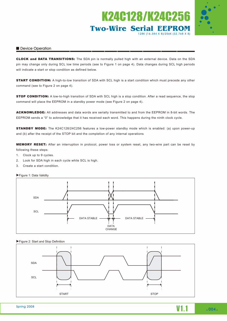
CLOCK and DATA TRANSITIONS: The SDA pin is normally pulled high with an external device. Data on the SDA
pin may change only during SCL low time periods (see to Figure 1 on page 4). Data changes during SCL high periods
will indicate a start or stop condition as defined below.
START CONDITION: A high-to-low transition of SDA with SCL high is a start condition which must precede any other
command (see to Figure 2 on page 4).
STOP CONDITION: A low-to-high transition of SDA with SCL high is a stop condition. After a read sequence, the stop
command will place the EEPROM in a standby power mode (see Figure 2 on page 4).
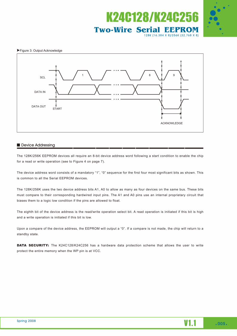
ACKNOWLEDGE: All addresses and data words are serially transmitted to and from the EEPROM in 8-bit words. The
EEPROM sends a “0” to acknowledge that it has received each word. This happens during the ninth clock cycle.
STANDBY MODE: The K24C128/24C256 features a low-power standby mode which is enabled: (a) upon power-up
and (b) after the receipt of the STOP bit and the completion of any internal operations
MEMORY RESET: After an interruption in protocol, power loss or system reset, any two-wire part can be reset by
following these steps:
1. Clock up to 9 cycles.
2. Look for SDA high in each cycle while SCL is high.
3. Create a start condition.
Figure 1: Data Validity
Figure 2: Start and Stop Definition
SDA
SCL
START STOP
SDA
SCL
DATA CHANGE
DATA STABLE DATA STABLE
V 1 . 1V 1 . 1Spring 2008 .005..005.
Figure 3: Output Acknowledge
Device Addressing
The 128K/256K EEPROM devices all require an 8-bit device address word following a start condition to enable the chip
for a read or write operation (see to Figure 4 on page 7).
The device address word consists of a mandatory “1”, “0” sequence for the first four most significant bits as shown. This
is common to all the Serial EEPROM devices.
The 128K/256K uses the two device address bits A1, A0 to allow as many as four devices on the same bus. These bits
must compare to their corresponding hardwired input pins. The A1 and A0 pins use an internal proprietary circuit that
biases them to a logic low condition if the pins are allowed to float.
The eighth bit of the device address is the read/write operation select bit. A read operation is initiated if this bit is high
and a write operation is initiated if this bit is low.
Upon a compare of the device address, the EEPROM will output a “0”. If a compare is not made, the chip will return to a
standby state.
DATA SECURITY: The K24C128/K24C256 has a hardware data protection scheme that allows the user to write
protect the entire memory when the WP pin is at VCC.
SCL
DATA IN
1
DATA OUT
8 9
ACKNOWLEDGE
START
128K (16,384 X 8) /256K (32,768 X 8)Two-Wire Serial EEPROM
K24C128/K24C256

V 1 . 1V 1 . 1
128K (16,384 X 8) /256K (32,768 X 8)Two-Wire Serial EEPROM
K24C128/K24C256
Spring 2008 .006..006.
Write Operations
BYTE WRITE: A write operation requires two 8-bit data word address following the device address word and
acknowledgment. Upon receipt of this address, the EEPROM will again respond with a “0” and then clock in the first
8-bit data word. Following receipt of the 8-bit data word, the EEPROM will output a “0” and the addressing device, such
as a microcontroller, must terminate the write sequence with a stop condition. At this time the EEPROM enters an
internally timed write cycle, tWR, to the nonvolatile memory. All inputs are disabled during this write cycle and the
EEPROM will not respond until the write is complete (see Figure 5 on page 7).
PAGE WRITE: The 128K/256K devices are capable of 64-byte page writes.
A page write is initiated the same as a byte write, but the microcontroller does not send a stop condition after the first
data word is clocked in. Instead, after the EEPROM acknowledges receipt of the first data word, the microcontroller can
transmit up to 63 more data words. The EEPROM will respond with a “0” after each data word received. The
microcontroller must terminate the page write sequence with a stop condition (see Figure 6 on page 7).
The data word address lower six (128K/256K) bits are internally incremented following the receipt of each data word.
The higher data word address bits are not incremented, retaining the memory page row location. When the word
address, internally generated, reaches the page boundary, the following byte is placed at the beginning of the same
page. If more than 64 data words are transmitted to the EEPROM, the data word address will “roll over” and previous
data will be overwritten.
ACKNOWLEDGE POLLING: Once the internally timed write cycle has started and the EEPROM inputs are disabled,
acknowledge polling can be initiated. This involves sending a start condition followed by the device address word. The
read/write bit is representative of the operation desired. Only if the internal write cycle has completed will the EEPROM
respond with a “0”, allowing the read or write sequence to continue.
Read Operations
Read operations are initiated the same way as write operations with the exception that the read/write select bit in the
device address word is set to “1”. There are three read operations: current address read, random address read and
sequential read.
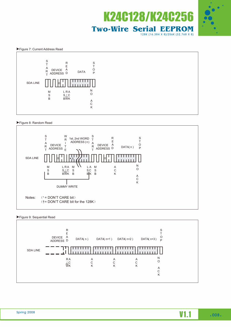
CURRENT ADDRESS READ: The internal data word address counter maintains the last address accessed during
the last read or write operation, incremented by one. This address stays valid between operations as long as the chip
power is maintained. The address “roll over” during read is from the last byte of the last memory page to the first byte of
the first page. The address “roll over” during write is from the last byte of the cur- rent page to the first byte of the same
page.
Once the device address with the read/write select bit set to “1” is clocked in and acknowledged by the EEPROM, the
current address data word is serially clocked out. The microcontroller does not respond with an input “0” but does
generate a following stop condition (see Figure 7 on page 8).

128K (16,384 X 8) /256K (32,768 X 8)Two-Wire Serial EEPROM
K24C128/K24C256
V 1 . 1V 1 . 1Spring 2008 .007..007.
Read Operations
RANDOM READ: A random read requires a “dummy” byte write sequence to load in the data word address. Once the
device address word and data word address are clocked in and acknowledged by the EEPROM, the microcontroller
must generate another start condition. The microcontroller now initiates a current address read by sending a device
address with the read/write select bit high. The EEPROM acknowledges the device address and serially clocks out the
data word. The microcontroller does not respond with a “0” but does generate a following stop condition (see Figure 8
on page 8).
SEQUENTIAL READ: Sequential reads are initiated by either a current address read or a random address read. After
the microcontroller receives a data word, it responds with an acknowledge. As long as the EEPROM receives an
acknowledge, it will continue to increment the data word address and serially clock out sequential data words. When
the memory address limit is reached, the data word address will “roll over” and the sequential read will continue. The
sequential read operation is terminated when the microcontroller does not respond with a “0” but does generate a
following stop condition (see Figure 9 on page 8).
Figure 4: Device Address
Figure 5: Byte Write
Figure 6: Page Write
1 0 1 0 0 A1 A0 R/W
MSB LSB
SDA LINE
START
MSB
DEVICE ADDRESS
LSB
R/W
ACK
MSB
FIRST WORD ADDRESS
WRITE
LSB
ACK
ACK
DATA
ACK
STOP
SECOND WORD ADDRESS
SDA LINE
Notes: (* = DON’T CARE bit) († = DON’T CARE bit for the 128K)
START
MSB
DEVICE ADDRESS
LSB
R/W
ACK
ACK
DATA( n )
ACK
ACK
STOPDATA( n+x )
WRITE
MSB
ACK
FIRST WORD ( n )ADDRESS
LSB
SECOND WORD ( n )ADDRESS
0
0
* †
* †
V 1 . 1V 1 . 1
0
Spring 2008 .008..008.
Figure 7: Current Address Read
Figure 8: Random Read
Figure 9: Sequential Read
SDA LINE
START
MSB
DEVICE ADDRESS
LSB
R/W
ACK
NO
ACK
STOP
READ DATA
SDA LINE
START
MSB
DEVICE ADDRESS
LSB
R/W
ACK
ACK
1st, 2nd WORD ADDRESS ( n)
WRITE
START
MSB
DEVICE ADDRESS
LSB
ACK
NO
ACK
STOP
READ DATA( n )
DUMMY WRITE
DEVICE ADDRESS
R/W
ACK
DATA( n )
ACK
ACK
DATA( n+1 ) DATA( n+2 )
READ
SDA LINE
ACK
NO
ACK
STOPDATA( n+3 )
MSB
Notes: ( = DON’T CARE bit) ( = DON’T CARE bit for the 128K)
0 0
128K (16,384 X 8) /256K (32,768 X 8)Two-Wire Serial EEPROM
K24C128/K24C256

V 1 . 1V 1 . 1Spring 2008 .009..009.
Absolute Maximum Stress Ratings
DC Supply Voltage . . . . . . . . . . . . . . . . .-0.3V to +6.5V
Input / Output Voltage . . . . . . . .GND-0.3V to VCC+0.3V
Operating Ambient Temperature . . . . . -40。C to +85。C
Storage Temperature . . . . . . . . . . . . -65。C to +150。C
Electrical Characteristics
CommentsStresses above those listed under "Absolute Maximum Ratings" may cause permanent damage to this device. These are stress ratings only. Functional operation of this device at these or any other conditions above those indicated in the operational sections of this specification is not implied or intended. Exposure to the absolute maximum rating conditions for extended periods may affect device reliability.
DC Electrical Characteristics
Applicable over recommended operating range from: TA = –40?C to +85?C, VCC = +1.8V to +5.5V (unless otherwise noted)Parameter
Supply Voltage
Supply Current VCC = 5.0V
Supply Current VCC = 5.0V
5.5
1.0
3.0
Max.
READ at 400 kHz
WRITE at 400 kHz
Condition
1.8
-
-
Min.
VCC1
ICC1
ICC2
Symbol
-
0.4
2.0
Typ.
V
Supply Voltage 5.52.5VCC2 - V
Supply Voltage 5.52.7VCC3 - V
Supply Voltage 5.54.5VCC4 - V
mA
mA
Supply Current VCC = 1.8V
Supply Current VCC = 2.5V
1.0
2.0
VIN = VCC or Vss
VIN = VCC or Vss
-
-
ICC1
ICC2
0.6
1.0
Supply Current VCC = 2.7V
Supply Current VCC = 5.0V
2.0
5.0
VIN = VCC or Vss
VIN = VCC or Vss
-
-
ICC3
ICC4
1.0
1.0
Unit
Input Leakage Current
Output Leakage Current
Input Low Level
Output Low Level VCC =1.8V
Output Low Level VCC =5.0V
Input High Level
Output Low Level VCC =3.0V
3.0
3.0
VCC X 0.3
0.2
0.4
VCC + 0.5
0.4
VIN = VCC or Vss
VOUT = VCC or Vss
IOL = 0.15 mA
IOL = 3.0 mA
IOL = 2.1 mA
-
-
-0.6
-
-
VCC X 0.7
-
ILI
ILO
VIL
VOL1
VOL3
VIH
VOL2
0.05
0.10
-
-
-
-
-
V
V
V
V
V
A
A
A
A
A
A
Pin Capacitance
Applicable over recommended operating range from TA = 25 。C, f = 1.0 MHz, VCC = +1.8VParameter
Input/Output Capacitance (SDA)
Input Capacitance (A0, A1, SCL)
8
6
Max.
VIN = 0V
Condition
-
-
Min.
CI/O
CIN
Symbol
-
-
Typ.
pF
pF
Unit
VI/O = 0V
128K (16,384 X 8) /256K (32,768 X 8)Two-Wire Serial EEPROM
K24C128/K24C256
V 1 . 1V 1 . 1
128K (16,384 X 8) /256K (32,768 X 8)Two-Wire Serial EEPROM
K24C128/K24C256
Spring 2008 .010..010.
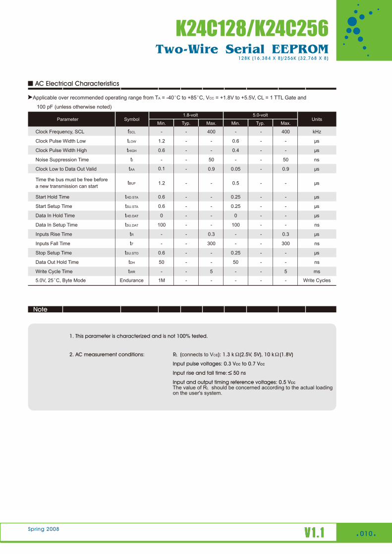
AC Electrical Characteristics
Applicable over recommended operating range from TA = -40。C to +85。C, VCC = +1.8V to +5.5V, CL = 1 TTL Gate and
100 pF (unless otherwise noted)
Note
Parameter
Clock Frequency, SCL
Clock Pulse Width Low
Clock Pulse Width High
Start Hold Time
Clock Low to Data Out Valid
Noise Suppression Time
Time the bus must be free before a new transmission can start
Start Setup Time
Data In Hold Time
Data In Setup Time
Data Out Hold Time
Write Cycle Time
Inputs Fall Time
Inputs Rise Time
Stop Setup Time
fSCL
tLOW
tHIGH
tHD.STA
tAA
tI
tBUF
tSU.STA
tHD.DAT
tSU.DAT
tDH
tWR
5.0V, 25。C, Byte Mode
-
1.2
0.6
0.6
0.1
-
1.2
0.6
0
100
50
-
-
-
0.6
1M
-
-
-
-
-
-
-
-
-
-
-
-
-
-
-
-
400
-
-
-
0.9
50
-
-
-
-
-
5
300
0.3
-
-
-
0.6
0.4
0.25
0.05
-
0.5
0.25
0
100
50
-
-
-
0.25
-
-
-
-
-
-
-
-
-
-
-
-
-
-
-
-
-
400
-
-
-
0.9
50
-
-
-
-
-
5
300
0.3
-
-
kHz
ns
ns
ms
ns
Write CyclesEndurance
tF
tR
tSU.STO
Max.Units
Min.Symbol
Typ.
1.8-volt
Max.Min. Typ.
5.0-volt
s
s
s
s
s
s
s
s
s
1. This parameter is characterized and is not 100% tested.
2. AC measurement conditions: RL (connects to VCC): 1.3 k (2.5V, 5V), 10 k (1.8V)
Input pulse voltages: 0.3 VCC to 0.7 VCC
Input rise and fall time: 50 ns
Input and output timing reference voltages: 0.5 VCC The value of RL should be concerned according to the actual loading on the user's system.
ns

V 1 .V 1 . 1Spring 2008 .011..011.
Bus Timing
Figure 10: SCL: Serial Clock, SDA: Serial Data I/O
Write Cycle Timing
Figure 11: SCL: Serial Clock, SDA: Serial Data I/O
Note
1. The write cycle time tWR is the time from a valid stop condition
of a write sequence to the end of the internal clear/write cycle.
SCL
SDA_IN
SDA_OUT
tFtLOW
tSU.STA tHD.STA
tAA tDH tBUF
tSU.STO
tR
tHD.DAT tSU.DAT
tHIGH
tLOW
8th BIT
SCL
SDAACK
STOPCONDITION
STARTCONDITION
tWR(1)
128K (16,384 X 8) /256K (32,768 X 8)Two-Wire Serial EEPROM
K24C128/K24C256

V 1 . 1V 1 . 1
128K (16,384 X 8) /256K (32,768 X 8)Two-Wire Serial EEPROM
K24C128/K24C256
Spring 2008 .012..012.
Ordering Information
1.Prefix
2.Series Name 24: Two-wire (I2C) Interface
3.EEPROM Density C128=128K bits
C256=256K bits
4.Design Option o= (Blank)
5.Package Type D = DIP
S = SOP
T = TSSOP
W = Wafer/die
6. Temperature Range C = Com Temp(0 。C-70 。C)
I = Ind Temp(-40 。C-85 。C)
E = Exp Temp(-40 。C-125 。C)
7.Pack Type T = Tube
R = Tape & Reel
8.Plating Technology Blank = Standard SnPb plating
G = ECOPACK(RoHS compliant)
9.Operating Voltage S=2.7~5.5
A=1.8~5.5
K 24 XXX X - X X X X X
1 2 3 4 5 6 7 8 9
Code Number
Part Number
Product Datasheet Change Notice
1.1 Datasheet Feb., 2008Version Content Date
Datasheet Revision History
128K (16,384 X 8) /256K (32,768 X 8)Two-Wire Serial EEPROM
K24C128/K24C256
V 1 . 1V 1 . 1Spring 2008 .013..013.
Disclaimers
The information in this publication has been carefully checked and is believed to be entirely accurate at
the time of publication. HUAJIE assumes no responsibility, however, for possible errors or omissions, or
for any consequences resulting from the use of the information contained herein.
HUAJIE reserves the right to make changes in its products or product specifications with the intent to
improve function or design at any time and without notice and is not required to update this
documentation to reflect such changes.
This publication does not convey to a purchaser of semiconductor devices described herein any license
under the patent rights of HUAJIE or others.
HUAJIE makes no warranty, representation, or guarantee regarding the suitability of its products for any
particular purpose, nor does HUAJIE assume any liability arising out of the application or use of any
product or circuit and specifically disclaims any and all liability, including without limitation any
consequential or incidental damages.
" Typ. " parameters can and do vary in different applications. All operating parameters, including " Typ. "
must be validated for each customer application by the customer's technical experts.
HUAJIE products are not designed, intended, or authorized for use as components in systems intended
for surgical implant into the body, for other applications intended to support or sustain life, or for any other
application in which the failure of the HUAJIE product could create a situation where personal injury or
death may occur.
Should the Buyer purchase or use a HUAJIE product for any such unintended or unauthorized application,
the Buyer shall indemnify and hold HUAJIE and its officers, employees, subsidiaries, affiliates, and
distributors harmless against all claims, costs, damages, expenses, and reasonable attorney fees arising
out of, either directly or indirectly, any claim of personal injury or death that may be associated with such
unintended or unauthorized use, even if such claim alleges that HUAJIE was negligent regarding the
design or manufacture of said product.
K24C Series (I2C Bus) Serial EEPROM
Data Sheet, Revision 1.1
2008 HUAJIE
All rights reserved. No part of this publication may be reproduced, stored in a retrieval system, or
transmitted in any form or by any means, electric or mechanical, by photocopying, recording, or
otherwise, without the prior written consent of HUAJIE.