serial control interface standard (rev 1.0) - analog devices · rev 1.0 5 adi-spi 1 scope the...
TRANSCRIPT

ADI-SPITechnical Specification
Serial Control Interface Standard (Rev 1.0)

ADI-SPI2Rev 1.0
Keywords SPI, SIF, Interface

ADI-SPI3Rev 1.0
Contents 1 Scope ........................................................................................................................................................ 5 1.1 Compliance ............................................................................................................................................................ 5
2 References ................................................................................................................................................ 5
3 Definitions, symbols and abbreviations ................................................................................................... 5 3.1 Definitions ............................................................................................................................................................. 5 3.2 Abbreviations ........................................................................................................................................................ 6
4 Physical Layer .......................................................................................................................................... 6 4.1 General .................................................................................................................................................................. 6 4.2 Pins ........................................................................................................................................................................ 6 4.2.1 CSB .................................................................................................................................................................. 6 4.2.2 SCLK ............................................................................................................................................................... 6 4.2.3 SDIO ................................................................................................................................................................ 6 4.2.4 SDO ................................................................................................................................................................. 6 4.3 Voltages and Interface Standards ......................................................................................................................... 7 4.4 Reference Configuration ....................................................................................................................................... 7 4.4.1 Minimum configuration .................................................................................................................................. 7 4.4.2 Three wire bus ................................................................................................................................................. 7 4.4.3 Four wire bus ................................................................................................................................................... 8 4.4.4 Mixed bus ........................................................................................................................................................ 8
5 Data Link .................................................................................................................................................. 8 5.1 General .................................................................................................................................................................. 8 5.2 Protocol ................................................................................................................................................................. 9 5.3 Instruction .............................................................................................................................................................. 9 5.3.1 Read/Write ....................................................................................................................................................... 9 5.3.2 Address ............................................................................................................................................................ 9 5.4 Data........................................................................................................................................................................ 9 5.4.1 Single Byte Writes........................................................................................................................................... 9 5.4.2 Streaming Bytes ............................................................................................................................................ 10 5.5 Timing ................................................................................................................................................................. 10 5.5.1 Write Cycle .................................................................................................................................................... 11 5.5.2 Read Cycle ..................................................................................................................................................... 11 5.6 Clock Domains .................................................................................................................................................... 11 5.6.1 Write Strobe Synchronization ....................................................................................................................... 11 5.6.2 Read Strobe Synchronization ........................................................................................................................ 12
6 Control .................................................................................................................................................... 12 6.1 General ................................................................................................................................................................ 12 6.2 Interface Configuration Register A 0x0000 ....................................................................................................... 12 6.2.1 Soft Reset ....................................................................................................................................................... 12 6.2.2 LSB First........................................................................................................................................................ 12 6.2.3 Address Ascension ........................................................................................................................................ 12 6.2.4 SDO Active ................................................................................................................................................... 13 6.2.5 Register 0x0000 Details ................................................................................................................................ 13 6.3 Interface Configuration Register B 0x0001 ....................................................................................................... 13 6.3.1 Single Instruction .......................................................................................................................................... 13 6.3.2 Bit 6 ............................................................................................................................................................... 13 6.3.3 Master Slave Readback Control .................................................................................................................... 13 6.3.4 Slow Interface Control .................................................................................................................................. 13 6.3.5 Bit 3 ............................................................................................................................................................... 14 6.3.6 Soft Reset 1 .................................................................................................................................................... 14 6.3.7 Soft Reset 0 .................................................................................................................................................... 14 6.3.9 Register 0x0001 Details ................................................................................................................................ 15 6.4 Device Configuration Register 0x0002 .............................................................................................................. 15 6.4.1 Operating Mode ............................................................................................................................................. 15 6.4.2 Custom Operating Mode ............................................................................................................................... 16 6.4.3 Device Status ................................................................................................................................................. 16

ADI-SPI4Rev 1.0
6.5 Chip Type 0x0003 ............................................................................................................................................... 16 6.6 Product ID 0x0004 & 0x0005 ............................................................................................................................. 16 6.7 Chip Grade 0x0006 ............................................................................................................................................. 16 6.8 Reserved 0x0007 ................................................................................................................................................. 16 6.9 Offset Pointer/Device Index 0x0008 .................................................................................................................. 16 6.10 Device Index 0x0009 .......................................................................................................................................... 17 6.11 Scratch Pad 0x000A ............................................................................................................................................ 17 6.12 SPI Revision 0x000B .......................................................................................................................................... 17 6.13 Vendor ID 0x000C & 0x000D ............................................................................................................................ 17 6.14 Reserved 0x000E ................................................................................................................................................ 17 6.15 Transfer Register ................................................................................................................................................. 17 6.15.1 Master-Slave Transfer Bit ............................................................................................................................. 17 6.16 Product Specific Memory ................................................................................................................................... 18 6.17 Power up delay .................................................................................................................................................... 18
7 Memory Map ........................................................................................................................................ 19
8 Example Timing Diagrams .................................................................................................................... 20 8.1 3-Wire Figures .................................................................................................................................................... 20 8.2 4-Wire Figure ...................................................................................................................................................... 20 8.3 MSB First Figures ............................................................................................................................................... 20 8.4 LSB First Figures ................................................................................................................................................ 20 8.5 Address Descension Figures ............................................................................................................................... 20 8.6 Address Ascension Figures ................................................................................................................................. 20 8.7 Write Operation ................................................................................................................................................... 20 8.8 Read Operation .................................................................................................................................................... 21 8.9 Timing Diagrams ................................................................................................................................................ 21
9 Application ............................................................................................................................................ 22 9.1 General ................................................................................................................................................................ 22 9.2 Reserved .............................................................................................................................................................. 22 9.3 Master-Slave Latching ........................................................................................................................................ 22 9.3.1 Software Synchronization ............................................................................................................................. 22 9.3.2 Pin Synchronization ...................................................................................................................................... 22 9.3.3 CSB Deactivation .......................................................................................................................................... 23 9.3.4 Delayed Synchronization .............................................................................................................................. 23 9.4 Pin & Function Re-Definitions ........................................................................................................................... 23 9.4.1 Conversion of SPI pins to Pin Mode Control by bus sequencing ................................................................ 23 9.4.2 Other options for conversion ......................................................................................................................... 24 9.4.3 Alternate Mapping ......................................................................................................................................... 24 9.5 Hard Reset/Soft Reset ......................................................................................................................................... 24 9.6 Device Discovery ................................................................................................................................................ 24 9.7 Optional SDO ...................................................................................................................................................... 24 9.8 Broadcasting ........................................................................................................................................................ 24 9.9 Blind Start-Up Operation and Regaining Interface Control .............................................................................. 24 9.10 Operation with mixed logic family devices ........................................................................................................ 24 9.11 Reserved .............................................................................................................................................................. 25 9.11.1 Reserved ........................................................................................................................................................ 25 9.11.2 Reserved ........................................................................................................................................................ 25 9.11.3 Reserved ........................................................................................................................................................ 25 9.11.4 Reserved ........................................................................................................................................................ 25 9.12 Reserved .............................................................................................................................................................. 25 9.13 Single Device Applications ................................................................................................................................ 25 9.14 Working with byte wide data .............................................................................................................................. 25 9.15 Working slow microcontrollers .......................................................................................................................... 26

ADI-SPI5Rev 1.0
1 Scope The purpose of this document is to define the physical specification that enables serial interface compatibility across ADI products for the primary purpose of device control and monitoring. The interface defined herein is generically defined as a SPI port and consists of chip or device select, clock, bi-directional data with an optional data out. This document also includes definition of frame structure to ensure consistency across products as well as a uniform map structure to simplify and standardize driver development for products conforming to this specification.
The specification is written with sufficient flexibility to allow interfacing to a wide range of controllers including FPGA, DSP, uC, RISC as well as SPI emulation with bit-banging when necessary.
1.1 Compliance All products that implement this interface should reference this protocol (ADI-SPI). In addition, those products should also clearly state their support for optional functionality listed in the table below.
Feature Description Section
3 wire or 4 wire The minimum interface consists of SCLK, CSB and SDIO. The 4th wire, SDO, is optional.
4.2.4 introduces the optional 4th wire (SDO)
Master-Slave Transfer
The minimum consists of core registers without buffering. Master-slave transfer registers are optional.
6.15.1
2 References JESD8-23 – Unified Wide Power Supply Voltage Range CMOS DC Interface Standard for Non-Terminated Digital Integrated Circuits
JESD8-5A.01 – 2.5V+/- 0.2V (Nominal Range) and 1.8V-2.7V (Wide Range) Power Supply Voltage and Interface Standard for Nonterminated Digital Integrated Circuits
JESD8-7A – 1.8V+/- 0.15V (Nominal Range) and 1.2V-1.95V (Wide Range) Power Supply Voltage and Interface Standard for Nonterminated Digital Integrated Circuits
Linux USB Project, http://www.linux-usb.org/usb.ids
3 Definitions, symbols and abbreviations
3.1 Definitions Data state of the SDIO or SDO pin Streaming is the process by which multiple bytes of data are written to or read from the slave device without
specifically providing instructions for each byte and is implemented by continually holding the CSB active and continuing to shift new data in or old data out of the slave device.
Master Slave Latch
A two stage memory where data is latched into the first stage based on one clock and then to the second stage with a different clock and is often used to ensure synchronization across clock domains. In this application, some registers may employ this technique to ensure special timing relationships are maintained. Those registers that utilize master slave latches will be clearly noted in the product datasheet.

ADI-SPI6Rev 1.0
3.2 Abbreviations CSB Chip Select Bar SCLK Serial Clock SDIO Serial Data Input/Output SDO Serial Output
4 Physical Layer
4.1 General
4.2 Pins The defined serial interface shall consist of SCLK, SDIO, CSB and SDO.
4.2.1 CSB
CSB is the chip select, an active low signal that selects the slave device with which the master intends to communicate. Typically, there is a dedicated CSB between the master and each slave. CSB is always driven by the master.
CSB also functions to synchronize and frame the communications to and from the slave device. When CSB is de-asserted and returned high, the controller completes the current access and returns the controller to the ready state awaiting the next instruction.
De-asserting CSB in the middle of a transaction aborts part or all of that transfer. If the transaction is aborted before the instruction is complete, no action is taken and the state machine returns to the ready state. If the transaction is aborted in the middle of the first data word, the transaction is aborted and the state machine returned to the ready state. If one or more complete data bytes have been completed after the instruction phase and before the abort occurs, those completed data bytes are written (or read), however any partial data bytes are aborted. See section 8.9 Timing Diagrams for examples of abort possibilities.
If CSB is de-asserted in the middle of a write to address 0x00 or 0x01, the soft reset bits (see section 6.2.1 Soft Reset, 6.3.6 Soft Reset 1 and 6.3.7 Soft Reset 0) may or may not occur. It is assumed that if the CSB is de-asserted in the midst of configuring these registers a system failure has occurred and the slave device will receive subsequent configuration commands. Otherwise, it is expected that slave operations would continue normally during this process.
4.2.2 SCLK
SCLK is the serial clock signal that synchronizes the slave device(s) to the master. Typically, SCLK is shared for all slave devices on the serial bus. SCLK is always driven by the master.
For both master and slave devices, data will be valid before the rising edge of SCLK and meet the respective setup and hold times.
4.2.3 SDIO
SDIO is the bi-directional data signal. Typically, SDIO is shared for all slave devices on the serial bus. SDIO is a bidirectional high impedance pin on both master and slave.
For compatibility, all devices must include bi-directional support in 3-wire mode which is the power up default. If 4-wire mode support is available, the SDO pin may be included and enabled by the user as part of interface configuration but the bi-directional capability of SDIO is still required, even if disabled during configuration. If 4-wire is enabled by configuring SDO, SDIO functions only as an input (SDI) until SDO is disabled.
4.2.4 SDO
SDO is the optional slave data output pin. Typically, SDO is shared for all slave devices on the serial bus. SDO is driven by only one slave device at a time, otherwise high impedance. SDO is always in high impedance while the slave CSB is false; otherwise assertion is controlled through the data link protocol. The only exception to this is when SDO has been assigned an alternate function as defined in section 9.4 Pin & Function Re-Definitions.

ADI-SPI7Rev 1.0
4.3 Voltages and Interface Standards In order to ensure as much compatibility as possible, devices implementing this standard will specify compliance to the most current version of one of the following standards: JESD8-23, JESD8-7A or JESD8-5A.01. The standard specified will be dependent on the processing node and supply voltage required. For each reference, the ‘wide range’ option should be specified to ensure as much inter-operation as possible. For standards that include class variations, the product will specify which class device is implemented. For information on connecting devices with mixed interface levels see section 9.10 Operation with mixed logic family devices.
Compliance to any JEDEC standard referenced is only a guideline and not a requirement for compliance with this document. The only requirement is that each product specify what logic standard is used.
4.4 Reference Configuration All devices that comply with this specification may coexist on a common bus. The following diagrams depict the supported wiring configurations of compliant devices. Other configurations are possible, but a) they must not interfere with the operation of supported devices, and b) they must be tolerant of supported devices as described in this specification.
4.4.1 Minimum configuration
4.4.2 Three wire bus

ADI-SPI8Rev 1.0
4.4.3 Four wire bus
4.4.4 Mixed bus
5 Data Link
5.1 General The CSB, SCLK, SDIO and optional SDO are used in conjunction to communicate with the slave device. Communication is separated into two distinct phases of operation. The first phase is the instruction phase and is used to initiate some action of the slave device and the second phase is the data phase which is either passed to the device to operate on or received from the device in response to the instruction phase. The instruction phase is treated as a 16-bit word and is shifted either MSB or LSB first depending on device configuration. The data phase is broken down into bytes then serialized into bits that are shifted either MSB or LSB first again based on device configuration. While MSB first is the default, the order may be changed by appropriately setting the interface configuration register.
CSB may be held low and multiple data bytes may be shifted during the data phase reducing the amount of overhead associated with data transfer. Sequential addresses may be sent in ascending or descending order based on how the configuration registers are set. Default for addressing sequential addresses is descending. By this technique one or more bytes may be written or read without having to provide an address for each.

ADI-SPI9Rev 1.0
5.2 Protocol There are two phases to a serial interchange. The first phase is the instruction cycle and is comprised of the controller shifting an instruction to the slave device. This is followed by one or more bytes of data shifted by the controller for a write operation or by the slave for a read operation.
5.3 Instruction Immediately following the falling edge of CSB that initiates a SPI cycle is the instruction phase. The instruction determines the action immediately following its completion. If the instruction is to write data to a target register, the following data bytes will be latched into 8 bit bytes and then routed to the target address starting with the one specified in the instruction phase. If the instruction is to read data from the target device, the address specified is the first address that the device will respond with at the completion of the instruction phase.
The instruction always consists of 16 bits and can directly address 0x7FFF addresses. A paging register can optionally be used if desired to either modify the address pointed to in the instruction or to be used as an index to simultaneously broadcast to multiple device as desired or required for a particular application. Implementation of either is optional and may be determined by the product specification. For details see section 6.9 Offset Pointer/Device Index 0x0008.
5.3.1 Read/Write
The most significant bit of the instruction phase is the read-write indicator bit. If this bit is set, the instruction represents a read instruction. If this bit is clear, the instruction represents a write instruction.
5.3.2 Address
The 15 LSBs of the instruction phase provide direct access to 0x7FFF registers, each representing 8 bits of data.
5.4 Data Data is always organized into 8 bit bytes and follows the instruction phase. As long as the CSB is asserted and while streaming is enabled, data continues until CSB is terminated for both read and write operations.
If a register requires more than 8 bits, sequential bytes in memory shall be utilized such that the lower address represents the lower significance byte. For example if 16 bits must be stored, the least significant byte should be placed in 0x0010 and the most significant byte stored in 0x0011. Although the basic unit of data is configured as 8 bit bytes, it is possible to interface with master devices that utilize larger units of storage. For additional details see 9.14 Working with byte wide data.
When a register requires more than 8 bits and spans 2 or more bytes and yet does not occupy the last byte fully, it is recommended that the data be LSB justified. That is the LSB of the register will be in bit 0 of the lowest byte as shown in the following.
MSB LSB
Position -> Bit 7 Bit 6 Bit 5 Bit 4 Bit 3 Bit 2 Bit 1 Bit 0
Address n Bit 7 Bit 6 Bit 5 Bit 4 Bit 3 Bit 2 Bit 1 Bit 0
Address n+1 n/a n/a Bit 13 Bit 12 Bit 11 Bit 10 Bit 9 Bit 8
5.4.1 Single Byte Writes
Single bytes of data may be written to or read from the slave device by returning CSB high after the one byte has been written or read regardless of the status of the configuration streaming bit. Alternately, a control bit is available (see 6.3.1 Single Instruction) that will force each data word to be preceded with a corresponding instruction even if CSB is not de-asserted.

ADI-SPI10Rev 1.0
5.4.2 Streaming Bytes
For operations that require large amounts of data to be passed to or from the slave device, streaming is supported. The instruction phase includes the starting address. The slave device starts reading or writing data to this address and continues as long as CSB is asserted and Single Byte Writes has not been enabled (6.3.1 Single Instruction). The slave device automatically increments or decrements the address depending on the setting of the Address Ascension bit in the configuration register. If the address is decrementing and 0x0000 is reached, the next address used is the top of the defined memory space as defined by the specific product. If the address is incrementing and the top of the product defined space is reached, the next address used is 0x0000. Care should be taken when writing to address 0x0000 as writing to this address may change the configuration of the serial interface. Therefore it is advised that 0x0000 be the first address written and that streaming stop prior to reaching this address.
Care should also be taken on devices that may include undocumented registers that default to specific values as streaming could overwrite these with incorrect values. In this case, undocumented registers that are user changeable should be include in the data sheet as values without description to ensure that should they be overwritten during streaming, are written with the correct values.
Streaming data can be very useful in a number of applications. In addition to simplifying the transfer of large amounts of data, streaming can facilitate the translation from larger storage units in the master by allowing the master to shift the larger units of data and the slave interpreting these as consecutive locations in the small, 8 bit target registers. See 9.14 Working with byte wide data for more details.
5.5 Timing The interface should be capable of reading and writing at speeds of at least 25 MHz (tCLK 40 nS). Hold time (tDH) should be less than 25% of the clock period. Setup time (tDS) should be less than 25% of the clock period. There is no minimum interface speed.
The following figures both represent acceptable timing diagrams. The only difference between the two is the initial state of the clock in regard to the CSB line. These diagrams do not indicate that the polarity of the clock can be changed to latch data on the rising or falling edge. In both cases, the rising edge of the SCLK is used to latch data.
Data setup and hold time is defined in the drawing above. Other important timing parameters are also shown.

ADI-SPI11Rev 1.0
Spec Name Meaning
tDS Setup time between data and rising edge of SCLK
tDH Hold time between data and rising edge of SCLK
tCLK Period of the clock
tS Setup time between CSB and SCLK
tH Hold time between CSB and SCLK
tHI Minimum period that SCLK should be in a logic high state
tLO Minimum period that SCLK should be in a logic low state
tZ Maximum time delay between CSB deactivation and SDIO or SDO bus return to high impedance.
tAccess Maximum time delay between falling edge of SCLK and output data valid for a read operation.
5.5.1 Write Cycle
The instruction word followed by the register data is written serially into the device through the SDIO pin on the rising edges of the interface clock, SCLK. The data can be transferred MSB first or LSB first depending on the setting of the LSB first register bit.
By default, the device is configured in MSB first mode and descending addressing. Both bit order and sequential addressing order can be changed through appropriate register configuration.
5.5.2 Read Cycle
The readback can be configured to use 3-wire or 4-wire (if supported) as described above and can be formatted with MSB first or LSB first. The instruction header is written to the device either MSB or LSB first (depending on the mode) followed by the data. By default, chip readback is sent via the SDIO (3-wire mode). Optional four-wire operation may be configured by setting the SDO Enable register. In 3-wire mode, the SDIO pin becomes an output pin after receiving the instruction header with a readback request. In this mode, the SDIO must be changed from an input to an output in the ½ cycle of SCLK between the last rising edge of SCLK of the instruction and the following falling edge. In 4-wire mode, the output drivers of the SDO enable after the last rising edge of SCLK of the instruction cycle and remain active until the end of the read cycle. When CSB is de-asserted, SDO returns to high impedance until the next read transaction.
Some master devices require extra time when transitioning between output and input. To facilitate this, a control bit is available. See 6.3.4 Slow Interface Control.
5.6 Clock Domains Generally, but not always, the device will have 2 or more clock domains. These typically are the SCLK described in this document and one or more device clocks. The SCLK is responsible for interfacing with hardware external to the device. Internally to the device, it is common for register actions to be synchronous to the device clock. In many cases writing to and reading from device registers must be synchronized across both clock domains to ensure that data is reliably passed between domains.
5.6.1 Write Strobe Synchronization
While the external mechanism to transfer data from the master to the slave register is defined elsewhere, the implementation will properly synchronize the externally generated write signal with the appropriate device clock to ensure that data is not in transition while the data bits may be in use by the device core.

ADI-SPI12Rev 1.0
5.6.2 Read Strobe Synchronization
While most device reads will be of static data, some register reads may be of dynamic data. In this case, the externally generated read strobe will be properly synchronized with the appropriate device clock to ensure that the data being read is stable during the entire read access.
6 Control
6.1 General Control of the slave device is achieved by accessing the memory map of the device. The memory map starts at 0x0000 and can extend as high as 0x7FFF. Individual addresses can be directly addressed through the instruction or an offset can optionally be utilized as discussed in section 6.9 Offset Pointer/Device Index 0x0008. The first 16 addresses are reserved for configurations that are common across all devices adhering to the standard. All other addresses may be assigned to product specific functions. While master slave buffering is optional for product specific registers location above 0x000F, master slave buffering is not allowed for registers between 0x0000 and 0x000F. Unless specifically stated, all features in these registers are required.
6.2 Interface Configuration Register A 0x0000 Register 0x0000 shall be the serial interface configuration register and is implemented as a 4 bit palindrome with each nibble a mirror of the other. This ensures that regardless of which way data is shifting, the device can be programmed should device synchronization be lost. Therefore when writing to this address, the palindrome is always required to be written so as to eliminate any ambiguity in configuring this register.
If the chip implements a hard reset either via memory map or an external pin, the function of the hard reset should be to return the device to the state achieved otherwise through power up. All registers including 0x0000 will resume their default values as if the device had just been powered up.
It is not necessary to write to 0x0000 if the default configuration meets the needs of the application. However, if the user must change the settings, it is expected that the user will write to this address before writing to any other and that once configured rewriting to this address would be the exception rather than the rule.
This register is not optional. This register is not buffered with a master slave latch.
6.2.1 Soft Reset
Bit 7 and bit 0 implement chip reset. Setting this bit implements a reset function otherwise equivalent to a hard reset with the exception that the bits of 0x0000 (this register) and the SPI state machine are unaffected. Additionally, any other registers not preloaded on a hard reset are unaffected.
6.2.2 LSB First
Bit 6 and bit 1 shall be the LSB First control bit. When this bit is set, the LSB is shifted first for all operations. When this bit is clear, the MSB is shifted first for all operations. The default for this bit is clear resulting in MSB first operation. In regard to the instruction phase, the entire 16 bits are reversed as a single word. If this bit is set, the LSB of the instruction phase is sent first. If this bit is clear, the R/W control bit will be sent first since it resides in the MSB position of the instruction. In a similar manner individual data bytes are processed MSB or LSB first based off the setting of this bit.
6.2.3 Address Ascension
Bit 5 and bit 2 shall be the Address Ascension control bit. When used in conjunction with streaming, Address Ascension causes sequential addresses to ascend in order. Address Ascension is enabled by setting this bit. When this bit is cleared, sequential addresses descend. The default for this bit is clear resulting in addresses descending in operation.
ADI-SPI13Rev 1.0
6.2.4 SDO Active
Bit 4 and bit 3 shall be the SDO Active bit. Devices that operate in 4-wire mode will enable SDO when this bit is set, the SDO output is the active output and SDIO becomes an input only pin. If this bit is clear, SDO is inactive and all input and output occur through SDIO. If the device is a 3-wire only device, then setting this bit has no effect on operation. The default for this bit is clear resulting in 3-wire operation.
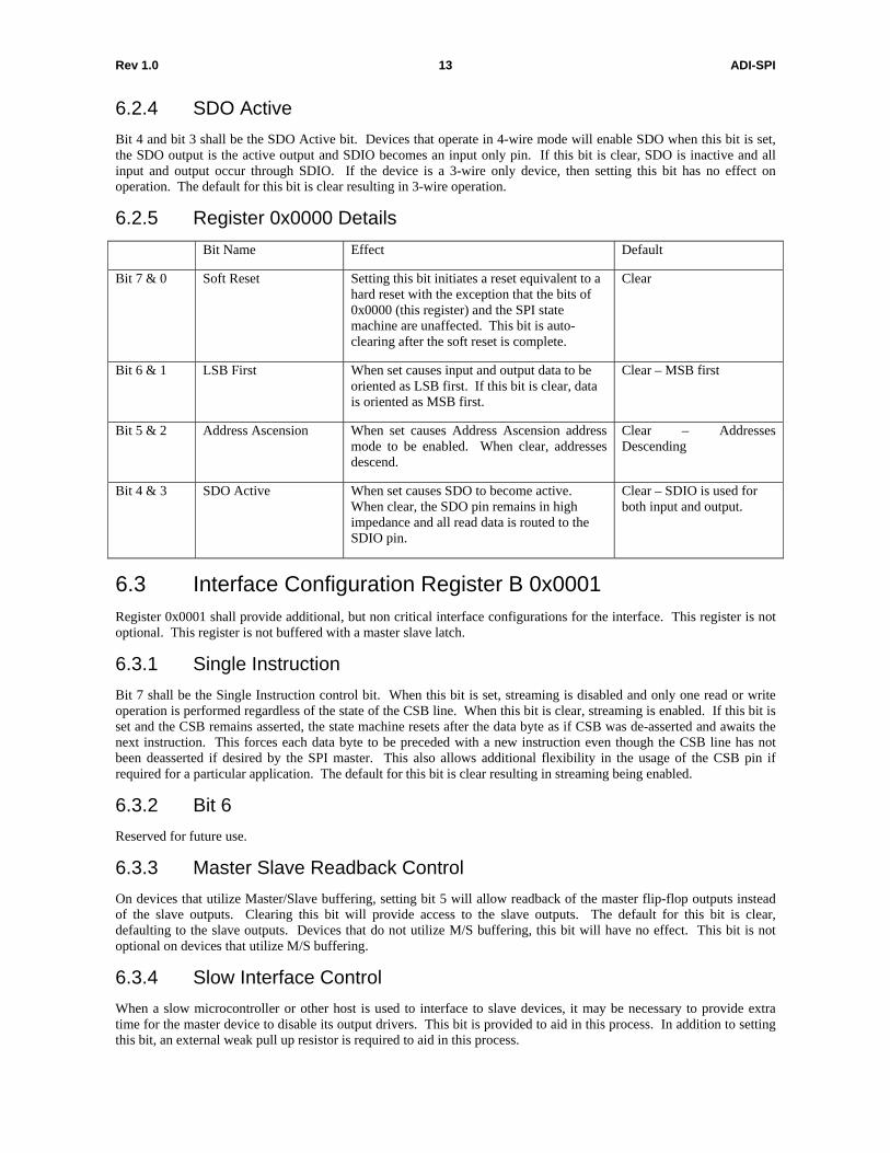
6.2.5 Register 0x0000 Details
Bit Name Effect Default
Bit 7 & 0 Soft Reset Setting this bit initiates a reset equivalent to a hard reset with the exception that the bits of 0x0000 (this register) and the SPI state machine are unaffected. This bit is auto-clearing after the soft reset is complete.
Clear
Bit 6 & 1 LSB First When set causes input and output data to be oriented as LSB first. If this bit is clear, data is oriented as MSB first.
Clear – MSB first
Bit 5 & 2 Address Ascension When set causes Address Ascension address mode to be enabled. When clear, addresses descend.
Clear – Addresses Descending
Bit 4 & 3 SDO Active When set causes SDO to become active. When clear, the SDO pin remains in high impedance and all read data is routed to the SDIO pin.
Clear – SDIO is used for both input and output.
6.3 Interface Configuration Register B 0x0001 Register 0x0001 shall provide additional, but non critical interface configurations for the interface. This register is not optional. This register is not buffered with a master slave latch.
6.3.1 Single Instruction
Bit 7 shall be the Single Instruction control bit. When this bit is set, streaming is disabled and only one read or write operation is performed regardless of the state of the CSB line. When this bit is clear, streaming is enabled. If this bit is set and the CSB remains asserted, the state machine resets after the data byte as if CSB was de-asserted and awaits the next instruction. This forces each data byte to be preceded with a new instruction even though the CSB line has not been deasserted if desired by the SPI master. This also allows additional flexibility in the usage of the CSB pin if required for a particular application. The default for this bit is clear resulting in streaming being enabled.
6.3.2 Bit 6
Reserved for future use.
6.3.3 Master Slave Readback Control
On devices that utilize Master/Slave buffering, setting bit 5 will allow readback of the master flip-flop outputs instead of the slave outputs. Clearing this bit will provide access to the slave outputs. The default for this bit is clear, defaulting to the slave outputs. Devices that do not utilize M/S buffering, this bit will have no effect. This bit is not optional on devices that utilize M/S buffering.
6.3.4 Slow Interface Control
When a slow microcontroller or other host is used to interface to slave devices, it may be necessary to provide extra time for the master device to disable its output drivers. This bit is provided to aid in this process. In addition to setting this bit, an external weak pull up resistor is required to aid in this process.

ADI-SPI14Rev 1.0
When this bit is set, the slave device will monitor the state of the SDIO line after the 16-bit instruction phase. A low to high transition on the SDIO line after the last SCLK edge of the 16-bit instruction indicates to the slave that the master output driver has been disabled. If a read instruction is indicated and this bit is set, then when a low to high transition is detected on the SDIO line, the SDIO line can be reconfigured as an output without causing a bus contention. It can stay in this state for the remainder of the current cycle as determined by the state of the CSB line.
If the last bit sent as part of the instruction phase is a zero, when the master goes into high-impedance preparing to function as an input, the external pull up causes the low to high transition. If the last bit as part of the instruction phase is a one, then the master must force a zero before setting the output as high-impedance. This bit is optional and provided for devices that are intended to interface to microcontrollers that must be manually changed between write and read processes. It is not intended to be used when interfacing to FPGAs or ASICs. On devices that do implement this function, setting this bit enables this function. If this bit is clear, interfacing as described in the remainder of this document is implemented.
6.3.5 Bit 3
Reserved for future use.
6.3.6 Soft Reset 1
Bit 2 functions as soft reset 1 which may be defined by the product definition as part of a tiered reset function. This function is optional. If not used, this bit must either be ignored by the state machine or should have the same effect as bit 7/0 of register 0x0000. This bit may be used in conjunction with Soft Reset 0 or independently.
6.3.7 Soft Reset 0
Bit 1 functions as soft reset 0 which may be defined by the product definition as part of a tiered reset function. This function is optional. If not used, this bit must either be ignored by the state machine or should have the same effect as bit 7/0 of register 0x0000. This bit may be used in conjunction with Soft Reset 1 or independently.
ADI-SPI15Rev 1.0
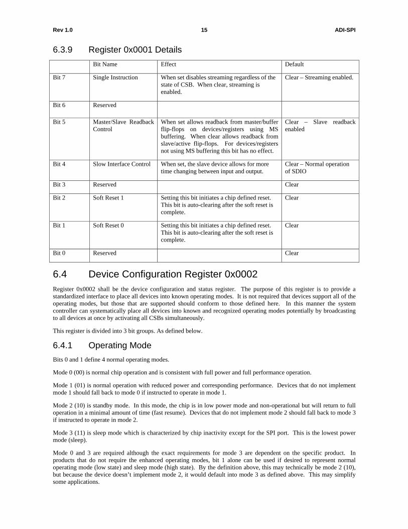
6.3.9 Register 0x0001 Details
Bit Name Effect Default
Bit 7 Single Instruction When set disables streaming regardless of the state of CSB. When clear, streaming is enabled.
Clear – Streaming enabled.
Bit 6 Reserved
Bit 5 Master/Slave Readback Control
When set allows readback from master/buffer flip-flops on devices/registers using MS buffering. When clear allows readback from slave/active flip-flops. For devices/registers not using MS buffering this bit has no effect.
Clear – Slave readback enabled
Bit 4 Slow Interface Control When set, the slave device allows for more time changing between input and output.
Clear – Normal operation of SDIO
Bit 3 Reserved Clear
Bit 2 Soft Reset 1 Setting this bit initiates a chip defined reset. This bit is auto-clearing after the soft reset is complete.
Clear
Bit 1 Soft Reset 0 Setting this bit initiates a chip defined reset. This bit is auto-clearing after the soft reset is complete.
Clear
Bit 0 Reserved Clear
6.4 Device Configuration Register 0x0002 Register 0x0002 shall be the device configuration and status register. The purpose of this register is to provide a standardized interface to place all devices into known operating modes. It is not required that devices support all of the operating modes, but those that are supported should conform to those defined here. In this manner the system controller can systematically place all devices into known and recognized operating modes potentially by broadcasting to all devices at once by activating all CSBs simultaneously.
This register is divided into 3 bit groups. As defined below.
6.4.1 Operating Mode
Bits 0 and 1 define 4 normal operating modes.
Mode 0 (00) is normal chip operation and is consistent with full power and full performance operation.
Mode 1 (01) is normal operation with reduced power and corresponding performance. Devices that do not implement mode 1 should fall back to mode 0 if instructed to operate in mode 1.
Mode 2 (10) is standby mode. In this mode, the chip is in low power mode and non-operational but will return to full operation in a minimal amount of time (fast resume). Devices that do not implement mode 2 should fall back to mode 3 if instructed to operate in mode 2.
Mode 3 (11) is sleep mode which is characterized by chip inactivity except for the SPI port. This is the lowest power mode (sleep).
Mode 0 and 3 are required although the exact requirements for mode 3 are dependent on the specific product. In products that do not require the enhanced operating modes, bit 1 alone can be used if desired to represent normal operating mode (low state) and sleep mode (high state). By the definition above, this may technically be mode 2 (10), but because the device doesn’t implement mode 2, it would default into mode 3 as defined above. This may simplify some applications.

ADI-SPI16Rev 1.0
6.4.2 Custom Operating Mode
Bits 2 and 3 define 4 potential device dependant operating modes. These modes may be used to augment operating mode 0 to optimize performance for a given configuration. These bits are optional. If used, 00 should represent normal mode with the other 3 modes being the modified operating conditions.
6.4.3 Device Status
Bits 4 through 7 are device dependant status bits. These are optional and may be specified by the product to convey certain device operating status not limited to but potentially including fault conditions, PLL lock status, reset status or any other operational condition required by the product. An active high state for these bits indicates proper functionality. As such, unused bits should be set high. A low state indicates improper operation. Additionally these status bits could be used in conjunction with a device interrupt if so equipped. By polling this register, the master can quickly determine what the interrupt or fault conditions are.
6.5 Chip Type 0x0003 This is a read only register and is required on all products whether Chip ID is used or not. This register uniquely defines the product type and is tied to the Chip IDs. The list of currently defined device types is shown in the following table. Device types 0 and 255 are invalid. This register is required.
Type Code Type Code
Not Assigned 00 & FF Precision ADCs 07
RF Products 01 Precision DACs 08
IF Products 02 Transceiver Products 09
High Speed ADCs 03 0A
High Speed DACs 04 0B
Clocks 05 0C
PLLs 06 0D
6.6 Product ID 0x0004 & 0x0005 Product ID is a unique ID assigned to each product and product type. Product ID spans 2 bytes. Product IDs 0x0000 and 0xFFFF are invalid. Product IDs may be duplicated on different chip types. This register is optional and may not be present on all devices.
6.7 Chip Grade 0x0006 Chip grade consists of two nibbles. The upper nibble should be used to indicate product variations such as speed grades or linearity grades used within a single product ID. The lower nibble should be used to indicate mask or trim variations. One or both nibbles are optional and may not be used on all products.
6.8 Reserved 0x0007 This register is reserved for future use.
6.9 Offset Pointer/Device Index 0x0008 This register is used as an offset pointer that is used to modify the address portion of the SPI instruction and may be implemented in several ways. It may be used as a direct offset added to the address portion of the SPI Instruction. It may also be used as a page offset to select alternate memory maps or to increase memory space beyond the 0x7FFF accessible by direct access. The third method is to use these 8 bits as device selects. In this mode, one or more on-chip devices will accept the write simultaneous like a broadcast. This mode is useful when the device contains identical copies of hardware (DACs, ADCs, Clocks, etc) that must receive the same configuration. In this case each device is

ADI-SPI17Rev 1.0
represented by a bit that is set if the instantiation is to receive the command. If clear, the instantiation does not receive the command. This register is optional.
6.10 Device Index 0x0009 This register is used in conjunction with 0x0008 and provides additional device index capability as defined in the previous section.
6.11 Scratch Pad 0x000A The scratch pad is used to provide a consistent location in memory that has guaranteed availability and unrestricted access. This register is primarily used for software debug and to validate bidirectional communication with the DUT in the end product. This register provides a benign location that can be used to test both the write and read process without impact to device configuration or operation. This register is required.
6.12 SPI Revision 0x000B This register is used to indicate the version of SPI implemented in silicon. Initial release will be set at 0x00. Additional updates will be notated in this section.
The value coded for this register should be as follows:
Version Coded value
Pre-release 0x00
Revision 1.0 (initial release) 0x01
6.13 Vendor ID 0x000C & 0x000D Many customers have requested a vendor ID be included in our devices. In order to self-differentiate from other vendors, the USB vendor ID list was chosen. Analog Devices Vendor ID is 0x0456 and may be viewed at http://www.linux-usb.org/usb.ids. Implementation of this register is not optional. This should be placed in memory such that 0x000C is set to 0x56 and 0x000D is set to 0x04.
6.14 Reserved 0x000E This register is reserved for future use.
6.15 Transfer Register
6.15.1 Master-Slave Transfer Bit
Bit 0 shall be used as the master-slave transfer bit if required by the device. The transfer bit is useful when a register is composed of multiple bytes that must all be written simultaneously to prevent erroneous device operation. Examples include NCO frequencies and PLL dividers. When this bit is set, data that has been entered into the master registers will be transferred to the slave. Upon completion of the transfer, the slave device will clear this bit (auto-clear) indicating to the SPI master that the transfer was complete and the slave data may be read back if desired by the control program. Prior to a transfer, an attempted readback would view the prior data unless bit 5 (Master Slave Readback Control) was set. In that case, the master data would be accessed. Another common method to invoke the transfer is to use the CSB low to high transition. Other methods may be defined and used if required by the product. This bit is optional and is only required in devices that require software control of transfer of data between master and slave registers. Devices that do not include this bit will complete the transfer when the current cycle is terminated as indicated by deselecting of the CSB line.

ADI-SPI18Rev 1.0
Bit Name Effect Default
Bit 7 Reserved Clear
Bit 6 Reserved Clear
Bit 5 Reserved Clear
Bit 4 Reserved Clear
Bit 3 Reserved Clear
Bit 2 Reserved Clear
Bit 1 Reserved Clear
Bit 0 Master-Slave Transfer Bit
When set causes a transfer of data from the master registers to the slave. This bit is auto-clearing after the transfer is complete. Ignored if the device doesn’t implement software synchronization.
Clear
6.16 Product Specific Memory Individual product memory space begins at 0x0010 and extends to address 0x7FFF if necessary. Memory locations less than 0x0010 are reserved as outlined in previous paragraphs.
Addressing need not be contiguous and clusters of addresses may be utilized for strategic purposes. In many instances it may be logical to assign different pages to related functions such that analog controls are on one page and digital controls are on a different page.
6.17 Power up delay At power up or after device reset, it may be necessary to transfer data from non-volatile RAM to device memory to load device defaults. This is typically done by instantiating an on chip SPI master that takes control of the internal SPI slave at power up or reset to load data into device memory. During this period, the external SPI interface may be unavailable. For each product that utilizes a mechanism that disables external SPI access, it should be clearly documented what the access delay is after power up or reset.

ADI-SPI19Rev 1.0
7 Memory Map Addr
(Hex) Parameter Name Bit 7
(MSB) Bit 6 Bit 5 Bit 4 Bit 3 Bit 2 Bit 1
Bit 0 (LSB)
Def. Value (Hex)
Default Notes and comments
Chip Configuration Registers
0x0000 interface_config_A Soft
Reset LSB First
Address Ascensi
on
SDO active
SDO active
Address Ascensi
on
LSB First
Soft Rest
00 Chip interface
configuration A
0x0001 Interface_config_B Single Instruction
Master/Slave
Readback
Control
Slow Interface Control
Soft
Reset 1 Soft
Reset 0 00
Chip interface configuration B
0x0002 device_config Status bit 3
Status bit 2
Status bit 1
Status bit 0
Optional customer operating modes
0 – normal operation mode
1 – low power normal operation
2 – medium power standby
3 – low power sleep mode
x0 Device
configuration registers
0x0003 chip_type
0 & FF – not assigned
1 – RF
2 – IF
3 – High Speed ADC
4 – High Speed DAC
5 – Clock
6 – PLL
7 – Precision ADC
8 – Precision DAC
9 – Transceivers
Defines the device type. Read only.
0x0004
product_ID
(low byte)
Unique Product ID managed by
each product team and is
clearly identified in customer
documentation to identify each
product. Chip IDs 0x0000 & 0xFFFF are not allowed. Read
only.
0x0005
product_ID
(high byte)
0x0006 chip_grade Product grade Device Revision
Defines product variations such as speed and
performance and device revisions.
Read only.
0x0007 reserved

ADI-SPI20Rev 1.0
Addr
(Hex) Parameter Name Bit 7
(MSB) Bit 6 Bit 5 Bit 4 Bit 3 Bit 2 Bit 1
Bit 0 (LSB)
Def. Value (Hex)
Default Notes and comments
0x0008
page_pointer
device index 00
Defines options address offset or
device index
0x0009 device index 00 Secondary
device index register
0x000A scratch_pad Used by SW to
test read & write
0x000B spi_revision 00 Initial release
0x000C Vendor ID low byte 0x56 0x56 Defined by
linux-usb.org 0x000D Vendor ID high byte 0x04 0x04
0x000E reserved
0x000F Transfer Register
Master-Slave
Transfer bit
8 Example Timing Diagrams The following are example timing diagrams for various modes of operation.
8.1 3-Wire Figures Figures 7, 8, 1, 2 and 11 show representative examples of 3-wire operation.
8.2 4-Wire Figure Figure 11 shows a representative example of 4-wire operation.
8.3 MSB First Figures Figures 7 and 8 show MSB first operation examples.
8.4 LSB First Figures Figures 1, 2 and 11 show LSB first operation examples.
8.5 Address Descension Figures Figures 7 and 8 show examples of Address Descension operation.
8.6 Address Ascension Figures Figures 2 shows and example of Address Ascension operation.
8.7 Write Operation Figures 7, 8, 1 and 2 show example write operations.

ADI-SPI21Rev 1.0
8.8 Read Operation Figure 11 shows an example of read operations.
8.9 Timing Diagrams
This figure shows a typical write sequence to the device streaming to 3 consecutive addresses.
In the top drawing CSB terminates the cycle during the middle of the instruction. In this case both instruction and any following data are ignored. In the bottom drawing, the cycle is not terminated until the second data has started. In this case, the instruction is processed and the data written to register n. Data for register n-1 is aborted and any following bits are ignored. If this had been a read instruction, the data associated with register n would be correctly captured by the master.
The drawing shows an example of the two phases of transfer in LSB first 3-wire read instruction.
ADI-SPI22Rev 1.0
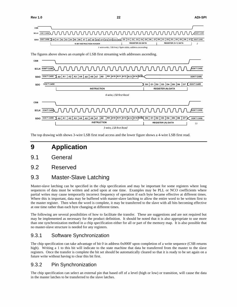
The figures above shows an example of LSB first streaming with addresses ascending.
The top drawing with shows 3-wire LSB first read access and the lower figure shows a 4-wire LSB first read.
9 Application
9.1 General
9.2 Reserved
9.3 Master-Slave Latching Master-slave latching can be specified in the chip specification and may be important for some registers where long sequences of data must be written and acted upon at one time. Examples may be PLL or NCO coefficients where partial writes may cause temporarily incorrect frequency of operation if each byte became effective at different times. Where this is important, data may be buffered with master-slave latching to allow the entire word to be written first to the master register. Then when the word is complete, it may be transferred to the slave with all bits becoming effective at one time rather than each byte changing at different times.
The following are several possibilities of how to facilitate the transfer. These are suggestions and are not required but may be implemented as necessary for the product definition. It should be noted that it is also appropriate to use more than one synchronization method in a chip specification either for all or part of the memory map. It is also possible that no master-slave structure is needed for any registers.
9.3.1 Software Synchronization
The chip specification can take advantage of bit 0 in address 0x000F upon completion of a write sequence (CSB returns high). Writing a 1 to this bit will indicate to the state machine that data be transferred from the master to the slave registers. Once the transfer is complete the bit set should be automatically cleared so that it is ready to be set again on a future write without having to clear this bit first.
9.3.2 Pin Synchronization
The chip specification can select an external pin that based off of a level (high or low) or transition, will cause the data in the master latches to be transferred to the slave latches.
ADI-SPI23Rev 1.0
9.3.3 CSB Deactivation
When CSB is deactivated, the cycle is considered complete. This state change could be used to transfer data from any master register to its slave.
9.3.4 Delayed Synchronization
Any of the previously specified methods may be used in conjunction with a programmable timer. The effect of the timer will be to delay the transfer from the master to the slave latches a pre-determined number of master clock cycles. The result of this will be to allow better synchronization with either an external or internal event.
9.4 Pin & Function Re-Definitions The definition of the SPI pins and functions can be changed if required by the product definition between this standard and an alternate. Examples include but are not limited to conversion to I2C, Pin Mode or conversion to a SPI mode compatible with a prior version of SPI. The method of conversion is defined by the product and could include a configuration pin, a configuration register in the SPI map, a power up sequence or a bus timing configuration. It is also possible to reconfigure some, but not all of the pins to alternate functions. For example, SDO may be converted to a MUX output to provide other non-SPI information to the controller.
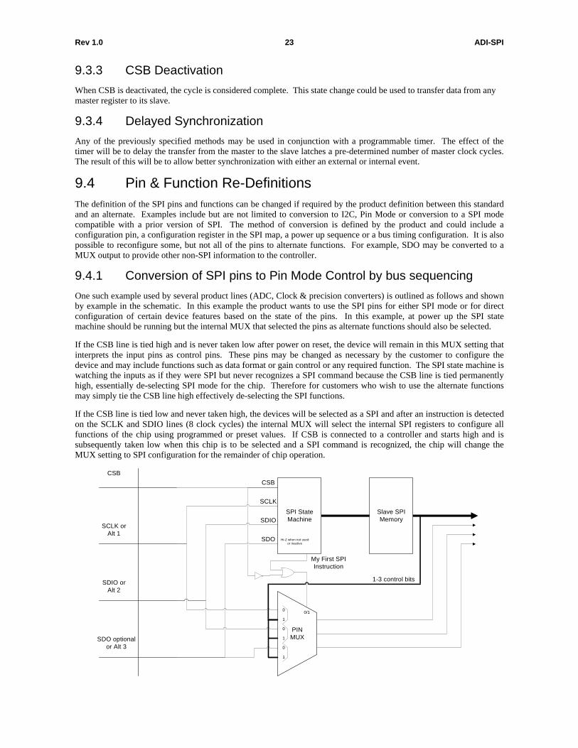
9.4.1 Conversion of SPI pins to Pin Mode Control by bus sequencing
One such example used by several product lines (ADC, Clock & precision converters) is outlined as follows and shown by example in the schematic. In this example the product wants to use the SPI pins for either SPI mode or for direct configuration of certain device features based on the state of the pins. In this example, at power up the SPI state machine should be running but the internal MUX that selected the pins as alternate functions should also be selected.
If the CSB line is tied high and is never taken low after power on reset, the device will remain in this MUX setting that interprets the input pins as control pins. These pins may be changed as necessary by the customer to configure the device and may include functions such as data format or gain control or any required function. The SPI state machine is watching the inputs as if they were SPI but never recognizes a SPI command because the CSB line is tied permanently high, essentially de-selecting SPI mode for the chip. Therefore for customers who wish to use the alternate functions may simply tie the CSB line high effectively de-selecting the SPI functions.
If the CSB line is tied low and never taken high, the devices will be selected as a SPI and after an instruction is detected on the SCLK and SDIO lines (8 clock cycles) the internal MUX will select the internal SPI registers to configure all functions of the chip using programmed or preset values. If CSB is connected to a controller and starts high and is subsequently taken low when this chip is to be selected and a SPI command is recognized, the chip will change the MUX setting to SPI configuration for the remainder of chip operation.
CSB
SDO optionalor Alt 3
SDIO orAlt 2
SCLK orAlt 1
PINMUX
SPI StateMachine
My First SPIInstruction
CSB
SDO
SDIO
SCLK
Hi-Z when not usedor inactive
Slave SPIMemory
1-3 control bits
0
1
0
1
0
1
0/1
ADI-SPI24Rev 1.0
9.4.2 Other options for conversion
Other conversion options may freely be defined by the product to suit the needs of the application and product but they may not interfere with system operation as defined in this document.
9.4.3 Alternate Mapping
Aside from different pin mapping, the SPI map can be changed through a similar process. This may be useful when the product must support legacy modes. In this case, instead of changing pin functions, the SPI map and/or protocol can be changed through a specified sequence, hardware or software. In general, this would not occur on the fly but would be more of an initial configuration to ensure compatibility with a previous SPI protocol or memory map. One implementation is already defined in 6.6 Product ID 0x0004 & 0x0005.
9.5 Hard Reset/Soft Reset If a hard reset is applied to the chip as defined by the chip specification, the serial interface must be reset to the default state with the contents of 0x0000 and 0x0001 forced to their default values. This puts the serial interface into a known communications mode and idling awaiting an instruction.
A chip soft reset should not affect the effect the serial communications registers located at 0x0000 and 0x0001.
9.6 Device Discovery With a structured chip type, product ID and chip grade it is possible to uniquely identify any device in any socket and programmatically load appropriate hardware and software drivers. It is recommended that the values in one or more of these registers be examined to determine what drivers or configuration files to load.
9.7 Optional SDO In designs that require low pin count or in applications where SDO is not needed, it may be omitted from the design. In these cases, 3-wire only mode is allowed. Any reference to SDO will be ignored by the state machine and read requests will be directed to the SDIO.
9.8 Broadcasting Communicating simultaneously with all devices at the same time is allowed by making more than one CSB lines active at once. In devices with identical memory maps this can be useful for configuring them at once rather than serially. Because the base map of devices conforming to this standard are the same, broadcasting to configure initial chip operation is automatically supported. Product specific broadcasting is also allowed when those memory maps are also identical. Broadcasting is only useful for writing to slave devices. Broadcasting is not supported for readback operations as asserting multiple CSBs during a read cycle would activate multiple outputs at the same time causing bus contention.
9.9 Blind Start-Up Operation and Regaining Interface Control If a hard reset fails to gain the attention of the slave device or if asserting a hard reset is detrimental to system operation, it is possible to gain the attention of the serial interface in the following manner.
Starting with the CSB de-asserted, assert the CSB for a non-multiple of 8 SCLK cycles. Then de-assert CSB. This should place the SPI state machine in a ready mode. Then assert the CSB line again. Write three bytes of 0x00. De-assert the CSB line. This will write all zeros into address 0x0000. Because this is a palindrome direction is unimportant and the address remains unique. This will force the SPI interface into the default state for writing to the device without impacting general operations of the chip. Other addresses can now be changed in the usual manner if desired. Core device operation should not be interrupted during this process providing a safe method for gaining access to a lost interface.
9.10 Operation with mixed logic family devices It is possible to easily interface mixed logic levels with a device from the ADG330x family of bidirectional bus translators such as the ADG3301/4/8. These devices are easily used to interface the SDIO between devices operating on different supply domains. One side of this device is connected to the master and the other side may be connected to

ADI-SPI25Rev 1.0
devices operating at high or lower supply voltages. Devices that operate on the same power domain as the master need not route through this device, only devices operating on different domains. It is also possible to use several of these, each operating on different secondary domains.
This device automatically detects which device is the driver and on which side of the device it resides appropriately changing the direction and drive to track this. This device should also work for SDO although there are other methods for dealing with unidirectional signals. All devices in this family work from 1.1 to 5.5 volts. When configuring these devices, the VCCA should be less than VCCY. Depending on which way the translations must occur, additional translators may be required. The family consists of singles, quads and octals as needed. For more details, consult one of the products data sheet.
9.11 Reserved
9.11.1 Reserved
9.11.2 Reserved
9.11.3 Reserved
9.11.4 Reserved
9.12 Reserved
9.13 Single Device Applications Setting bit 7 of address 0x0001 forces the state machine to interpret every operation as a single command without the need to de-assert the CSB each time. One application of this would be to tie the CSB low in a single device application to always enable the device. For some applications, this may simplify the configuration. While this should work in most instances, care must be taken as one of the key functions of the CSB line is to ensure synchronization with the master. Each time CSB is de-asserted, the state machine is reset. It CSB is never de-asserted, the state machine does not receive the reset and synchronization could be lost. If the application can guarantee the fidelity of SPI signals, then the device itself does not require CSB de-assertion.
9.14 Working with byte wide data While data registers are 8 bits in this standard, many SPI masters may be developed around 16, 32 or 64 bit SPI masters. In these cases, the output shifters used my be limited to minimum shift sizes that are larger than the 8 bit target registers of these devices. This should not pose any problems when developing drivers on these platforms if the developer simply maps the 8 bit registers of these slave devices to the larger words supported on the SPI master platform. For example, if the SPI master is based on 16 bit words without direct support for bytes, the developer can simply map two consecutive 8 bit words of the slave to one 16 bit word on the master. As such, addresses 0x0000 and 0x0001 can be mapped to a single operation of the master. Because the devices covered by this standard support streaming, the slave device would interpret this as writing two 8 bit words even though the master grouped them together as one 16 bit word.

ADI-SPI26Rev 1.0
This concept can be extended to larger shift units if necessary. This operation can be further simplified in some applications by setting the address ascension bit in register 0x0000.
9.15 Working slow microcontrollers In some applications, the SPI master may be a slow microcontroller that is incapable of changing the direction of its SDIO (that is the SPI masters SDIO) before the slave device enables its output drivers. In this case, to prevent bus contention issues, it may be necessary to operate the slave device in 4 wire mode. Other methods are possible, but this application method should resolve the issue on devices equipped to operate in 4 wire mode. For additional options, see 6.3.4 Slow Interface Control.