sensors and mems design - eproductalert.comeproductalert.com/digitaledition/sensors/sensors and mems...
TRANSCRIPT

Purchasing guides for the electronics industry
Platinum Sponsor:
Sensors and MEMS DesignResource Catalog 2009
www.eecatalog.com/sensors

Paying through the nosefor your EDA tools?
© 2009 Tanner Research. All rights reserved. Speeding Concept to Silicon
Corporate Headquarters825 South Myrtle AvenueMonrovia, CA 91016-3424 USATel: +1-626-471-9700Toll Free: 877-325-2223Fax: +1-626-471-9800Email: [email protected]: www.tannereda.com
Tanner EDA, #1 in analog mixed-signal IC designTo learn more go to www.TannerEDA.com or call +1 626-471-9701.Going to DAC? Stop by at booth #3655.
Find out why 25,000 engineers worldwide useTanner EDA, the affordable high-performance solution.
SCHEMATICCAPTURE
PHYSICALLAYOUT
PHYSICALVERIFICATION
PARASITICEXTRACTION
ANALOGSIMULATION
S-Edit™ L-Edit™ HiPer Verify™ HiPer PX™T-Spice™
Verilog-A

www.eecatalog.com/sensors �
Welcometothe2009SensorsandMEMSDesignResourceCatalog
Evolving interfaces are crucial to the development of technology and markets. Sensors, the interface between our analog, push and pull world and magical realm of digital processing, are becoming faster, more accu-rate, power-independent and incredibly diverse. This is accelerating every aspect of technological change. The reliability and accuracy of our sensors frame decisions from convenience in a smart home to life critical deci-sions in the air.
In our featured article, award-winning technology jour-nalist and Editor in Chief of the System-Level Design Community, Ed Sperling, takes us on a tour of the tech-nology. “Sensing Change” includes perspectives from all the major players and tracks the latest trends from stainless steel keyboards to talking trees to medical labs on a dot.
The interface between vendor and customer is just as important. That’s where this resource catalog comes in. It is your year-long reference to the best products and services from top manufacturers and suppliers.
Inside are the data sheets and detailed ads you need to make your best decisions. You will find new products to study and new ideas to build on. This is your essential guide for a growing year.
Please send your feedback, thoughts and comments to:
John BlylerEditorial Director
P.S. To subscribe to our series of Resource Catalogs for developers and other professionals, visit
www.eecatalog.com
Sensors and MEMS Design Resource Catalog 2009www.eecatalog.com/sensors
VP/Associate PublisherClair Bright [email protected](415) 255-0390 ext. 15
EditorialEditorial DirectorJohn Blyler [email protected](503) 614-1082
Creative/ProductionProduction DirectorStephanie Rohrer
Graphic DesignersKeith KellyBrandon Solem
Production Coordinator Kali Snowden
Online DirectorJeff Cheney
Advertising/Reprint SalesVP/Associate Publisher Embedded Electronics Media GroupClair Bright [email protected](415) 255-0390 ext. 15
Sales ManagerMarcy Carnerie [email protected] (510) 919-4788
Marketing/CirculationJenna Johnson
To Subscribewww.eecatalog.com/subscribe
Extension Media, LLCCorporate OfficePresident and PublisherVince [email protected]
Vice President, Sales Embedded Electronics Media GroupClair [email protected]
Vice President, Marketing and Product DevelopmentKaren [email protected]
Vice President, Business DevelopmentMelissa [email protected]
Special Thanks to Our Sponsors
The Sensors and MEMS Design Resource Catalog 2009 is published by Extension Media LLC. Extension Media makes no warranty for the use of its products and assumes no responsibility for any errors which may appear in this Catalog nor does it make a commitment to update the information contained herein. Sensors and MEMS Design Resource Catalog is Copyright ®2009 Extension Media LLC. No information in this Catalog may be reproduced without expressed written permission from Extension Media @ 1786 18th Street, San Francisco, CA 94107-2343.
All registered trademarks and trademarks included in this Catalog are held by their respective companies. Every attempt was made to include all trademarks and registered trademarks where indicated by their companies.

SensorsandMEMSDesignResourceCatalog20092
ContentsSensing Change
by Ed Sperling ............................................................................................................................................................................................4Cooling Rates Up to 100 Times Greater Than Other Systems
by Parker .................................................................................................................................................................................................... 7Accelerometers in the Bird’s Nest
by Tanner EDA ........................................................................................................................................................................................... 8Intelligent Medicine and Integrated Circuits
by Tanner EDA ......................................................................................................................................................................................... 10Highly Accurate, Compact USB Power Sensors up to 18 GHz by Anritsu
by Anritsu Company ................................................................................................................................................................................. 12
Products and Services
Signal ConditioningAmplifiers
AvagoTechnologiesACPL-C78A/C780/C784 miniature isolation amplifier .......... 13
MEMSHardware
KavlicoP6050/P6060 PCB Mount Pressure Sensors ......................... 15LeisterTechnologiesMEMs-based Mid-Infrared Sources ..................................... 16SporianMicrosystems,Inc.AssetOverseer ‘SS’ accelerometer/inertial shock sensor ....... 17
Software/DesignTannerEDAEVI - CALIBRE® INTEGRATION .............................................. 18
HiPer Verify - Physical Verification Tools .............................. 19L-Edit MEMS ......................................................................... 20L-Edit MEMS Design ............................................................. 21L-Edit - Physical Design Tools ............................................... 22T-Spice - Analog Simulation Tools ........................................ 23
Data Acquisition
MicrocontrollersMicrochipTechnologyInc.World’s First 16-bit Microcontrollers With 64 Kbytes of Flash in 28-pin Packages .................................................. 24SiliconLaboratoriesLow Power Mixed-signal 8-bit MCUs ................................... 25
ModulesPerpetuumLtdPMG37 .................................................................................. 26
Sensors and MEMS Design Resource Catalog OnlinEExplore...➔ Directory of leading sensors and MEMS Solutions
➔ Top Stories and News
➔ White Papers
➔ Expert Opinions (Blogs)
➔ Exclusive Videos
➔ Valuable Articles
➔ Ask the Experts
Sign up for the quarterly Sensors and MEMS Design E Product Alert
www.eecatalog.com/sensors

ESC Boston is a must-attend event for embedded systems engineers. You can customize your educational experience by selecting from over 85 sessions in 20 tracks specific to your interests. It is the place for you to identify solutions to immediatedesign challenges and meet in person thesolution providers for your next project.
ESC Boston is the place for the embedded community to learn today to design tomorrow. Register now at www.embedded.com/boston
2 Keynotes. 85 Sessions.75 Speakers.
Training + Education=All the Answers You Need.
Register Today.www.embedded.com/boston
We Speak Embedded.
Boston Hynes Convention Center
Robert BrunnerCEO of AmmunitionRenowned IndustrialDesigner of such productlines as the Apple II,Macintosh, Newton, and PowerBook
Design Excellence
Driving Corporate Excellence
T.J. RodgersFounder, President, Chief Executive Officer & Director ofCypress Semiconductor Corp.

Sensors and MEMS Design Resource Catalog 2009�
by Ed Sperling
Industry Forecast
Sensing ChangeBetter technology, better electronics and better measurement transform sensor market.
Sensors are changing. The interface between the digital processing world and the analog world with which we interact are becoming faster and more accurate. They are gathering more information with more intelligence about what gets imported and how often. And in some cases they are becoming far more stylish, drawing less power—sometimes measured in microwatts—and being applied to new applications where they have never had a role.
At least some of that change is being driven by the electronics around the sensors. It’s possible now to utilize more information differently. VC Kumar, product manager for Texas Instruments’ CC430 microcontroller, said there are three macro trends that are affecting the sensor world:
• Demand formoredatawithmore intelligence tomakemorereal-timedecisions;
• Theproliferationofwirelesstechnologiesforcommunication,par-ticularlyindevelopingcountrieswherethereneverhasbeenawiredinfrastructure,and
• Theemphasisonlowpowerandgreentechnology.
All of these factors have created new markets and new interest in sensors that can communicate wirelessly, particularly if they also include an embedded microcontroller to process data at the point of acquisition to figure out what goes to the host computer.
“If you think about a large building, you can automatically tell when a light goes out and know exactly where it is,” said Kumar. “You also can remotely dim or brighten an area in a building, and you can tell when a smoke alarm is no longer working.”
TI is heavily investing in energy harvesting technology, as well, so these sensors can work without batteries for a single duty cycle. A mesh network of sensors embedded in a road, for example, can harvest energy from the vibration of cars on the roadway and communicate regularly with a host computer. So when a bridge is under stress, for example, it gets reported well before the bridge is in danger of collapsing—something that is particularly important in earthquake-prone areas where damage isn’t always visible from the outside.
“This acts as a strain gauge, and when it reaches a certain limit it can set off alarms,” he said. “From a maintenance standpoint it’s great, too because there are no batteries. These devices can be embedded into the road or the bridge.
Those same devices can be embedded into trees—there is technology under development to power electronic shims from the PH difference between the soil and the tree, and from the acid in fruit—so when hardwood trees are being illegally
harvested or a fire has just started, that information can be sent wirelessly to a host computer.
Sensors in motionIn the consumer market, accelerometers based on MEMS chips are more than just the next big thing. They are arguably the biggest thing to come along in the history of the electronic sensor world. The iPhone popularized it with the landscape/portrait view and the Wii popularized it with its motion-based interactive video games. But it’s beginning to show up in a variety of places no one ever anticipated.
Wayne Meyer, MEMS marketing and application manager at Analog Devices, said motion is showing up in everything from touch screens to industrial products for safety reasons. It’s also showing up in cars in combination with gyroscopes to make sure a car isn’t tilting too far in a turn, for example, and in danger of spinning out of control or rolling over.
“You can thank or curse Apple for this,” said Meyer. “Now, if you don’t have that level of interaction, people think of a product as garbage. But motion sensing also is showing up in industrial and medical instrumentation. In hospitals, they’re putting accelerometers into IV poles so they don’t tip over. In construction, they’re using them in manned buckets so they can control the position of the person working there.”
MEMS chips already are present in pressure sensors, inkjets and microphones, and there is work under way to create labs on a chip so a drop of blood or saliva can be analyzed in seconds. In some cases, the amount of data being gathered is minimal. In others, such as a three-axis accelerometer combined with a gyroscope, it requires an immense amount of processing.

www.eecatalog.com/sensors �
“What we’re seeing now is the shift from ability to harvest and harvest more optimally,” said Meyer. “This is showing up in solar arrays that can track the sun and position themselves for optimal power. It’s also showing up in predictive motion for a motor, so when there’s excess vibration or an anomaly, it can either adjust itself or send a message that it needs maintenance.
Gleaming metalWhile work is underway to make sensors do things they could never do before, there’s also work to make sensing technology more appealing and useful in a variety of environments. Ordinary capacitive touch pads—the kind you might find on your oven or washing machine—are getting a makeover with inductive touch pads. Instead using plastic buttons or smooth pressure-sensitive glass or plastic, inductive sensors allow companies to use sheet metal.
In an industrial or medical setting, this means the keypad is virtually indestructible. In a hospital, for example, a keyboard can be wiped clean with disinfectant. And on a kitchen appliance, it can be built directly into the stainless steel.
“The advantage of inductive touch sensors is that you can a solid metal sheet instead of cutting out holes for a keypad,” said Keith Curtis, technical staff engineer with Microchip’s Security, Microcontroller & Technology Development Division. “In a harsh environment, you can seal out everything. What inductive touch allows you to do is to sense movements in metal.”
Microchip has filed a patent on the technology, which can use any conductive metal. Curtis said this technology has applications in medical, food preparation, automotive, home appliances and a variety of industrial applications. He said the technology is more expensive and draws more power than capacitive touch sensors, but the advantage is the board can be mounted directly to the chip, which makes it far more durable over time. He expects the market for this technology to begin heating up over the next 6 to 12 months.
Better measurements, new materialsAt least part of what’s behind all of these shifts in the sensor market is better interaction between the measurements and the sensors themselves, and different ways of taking measurements in the first place.
“Data acquisition systems, manufacturing test and process control allow sensors to make much more accurate measurements than in the past,” said Brian Betts, senior group manager for data acquisition at National Instruments. “They also allow sensors to go in new places. Historically, you needed an electrical current that went to a PC. Now we can use fiber optic cable to take measurements, and we can use a laser or light source to send light waves. Fiber bragg grating (which reflects particular wavelengths) can be inscribed into the fiber core. It behaves like a wavelength filter. As temperatures change, wavelengths shift.”
The accuracy is higher, because there is more data being sent from fiber-optic sensors. It also can be used in places where electromagnetic interference is high, such as turbines, or where electrical measurements are potentially dangerous, such as oil and gas exploration and testing.
“The general trend is more sensors and better interaction between technology, said Betts. “MIT came up with the concept of the Internet of Things. It’s not computers to computers. It’s machines to machines. A refrigerator can talk to your oven, or in weather research you can have sensors communicating with each other to gather information. Sensors are being used to get new information, but they’re also being put into new places.”
The bottom lineGiven the growing number of applications for sensors, as well as cheap processing to manage the data, demand for sensors is exploding. Most companies expect that demand to continue rising for years as sensors are put to new uses. That means more investment and more creativity in how they are deployed, how they are powered, and how the data is used on the back end.
For a technology that has been around for decades, it seems as if all the pieces are in place for the first time to record, process and react to data from sensors in multiple dimensions and multiple markets. And given the development activity at many large electronics companies working in this space, it’s certain these trends haven’t gone unnoticed.
Ed Sperling is Contributing Editor for Embedded Intel® Solutions and the Editor-in-Chief of the “System Level Design” portal. Ed has received numerous awards for techni-cal journalism.

Connections for Design SuccessNow, more than ever, knowing which design tools, IP, test, and manufacturing processes to use makes all the difference for design success. No other event gives you the opportunity to interact with the community of researchers, designers, and tool developers who enable the electronic design process. Invest your time in efficiency and productivity – attend DAC.
Mark your calendars for the 46th Design Automation Conference (DAC) at the Moscone Center, July 26-31, 2009, in San Francisco, California, USA.New DAC User Track: Over 90 technical paper and poster presentations on design tool use and methodology – by design engineers for design engineers! Learn how your peers have solved challenging problems with novel approaches and solutions.
Only DAC offers:• A robust technical program covering the latest research
developments and trends, ranging from management practices to products, methodologies and technologies for the design of SoCs, FPGAs, ASICs, analog and digital ICs, and more.
• Conveniently located in San Francisco – close to the East Bay, Silicon Valley and SFO.
• Worldwide attendance from developers, designers, researchers, academics, managers and engineers from leading electronics companies and universities.
• A vibrant exhibition with over 200 companies with solutions covering the electronic design eco-system from concept to silicon. Check out the new IC Design Chain Pavilion featuring IP, design and foundry services, PLUS the FREE sessions in the DAC Pavilion and the Exhibitor Forum.
Make DAC your one stop this year for networking, technical insights, and to find all the products and services you need to stay competitive. DAC – Where electronic design meets.IEEE members receive discounted member registration. Register Today.
www.dac.com
IEEEadDAC.indd 1 4/13/09 1:51:11 PM


www.eecatalog.com/sensors 9
About Tanner EDA
Tanner EDA is a leading provider of PC-based electronic design automation (EDA)software solutions for the design, layout and verification of analog/mixed-signal ICS, ASICs and MEMS. Its solutions help speed designs from concept to silicon and are used by thousands of companies to develop devices cost-effectively in the biomedical, consumer electronics, next-generation wireless, imaging, power management and RF market segments. Founded in 1988, Tanner EDA is a division of privately held Tanner Research, Inc.
Corporate Headquarters825 South Myrtle AvenueMonrovia, CA 91016-3424 USATel: +1-626-471-9700Toll Free: 877-325-2223Fax: +1-626-471-9800Email: [email protected]: www.tannereda.com
© 2009 Tanner Research. All rights reserved.All other company and/or product names are the property of their respective owners.
FEATURED CUSTOMERMEMSIC, Inc.Andover, Massachusetts, USA
INDUSTRY/APPLICATIONMicro-Electro-Mechanical Systems (MEMS) built into high-performance, low-cost accelerometers.
THE SITUATIONTo keep costs low and performance high, the company needs to design both MEMS-based accelerometers and integrated mixed signal circuitry for production in a standard CMOS IC process.
THE SOLUTIONMEMSIC has relied on the flexibility of Tanner Tools since 1999 to design standard CMOS layers into 2-axis and 3-axis MEMS accelerometers containing containing both a thermal sensor and analog circuitry.
TANNER EDA TOOLSHiPer Silicon Suite:
S-Edit - Schematic CaptureT-Spice - Analog SimulationL-Edit - Physical LayoutHiPer Verify - Physical Verification (DRC/LVS)Custom PDKs
For the current generation of accelerometers, MEMSIC eng ineer s use MEMS Pro, an application from SoftMEMS built on top of Tanner Tools for designing and analyzing MEMS. In fact, early MEMSIC products were even simpler and did not require full mechanical simulation, so the MEMSdesigners worked directly in Tanner Tools.
The engineers at MEMSIC use MEMS Pro for 3D mechanical model extraction for finite element analysis. They use L-Edit to modify the details of the sensor and for layout. After layout they use Tanner L-Edit Standard DRC and LVS. Finally, they export from L-Edit to a GDS layout file and send the result to tapeout for TSMC.
MEMS Designs, CMOS Fabrication
To take advantage of lower fabrication costs, MEMSIC designs its sensors almost exclusively with standard CMOS layers: for example, the heater is gate polysilicon and the first layer of the thermopile is metal and polysilicon.
“We have a tremendous advantage over our competitors,” continues Yongyao.
“Our process is almost independent of the fabrication foundry because our design is 95-99% CMOS. We can easily change process and foundry to take advantage of better production pricing. Our competitors, on the other hand, use proprietary MEMS processes, fabricating e i ther by themselves or through aspecialized foundry, and that is always more expensive than working with a traditional CMOS foundry.”
M EMSI C a l so en joys an advantage when changing geometry. Most of its competitors are still producing at 1-2
micron, and a change to 0.25 micron in MEMS would result in a completely different process and a costly conversion. MEMSIC has produced in 0.60 and 0.25 micron – with 0.18 micron on the roadmap
– and its standard CMOS IC process allows it to ramp up volume and production quickly after a change in geometry.
92,000 Accelerometers in Beijing
The marquee application of MEMSIC’stechnology was in the electronic “Waving Torch” distributed to all attendees of the opening ceremonies at the “Bird’s Nest”Stadium for the 2008 Olympics in Beijing.
The torch resembles a 20-30 cm wand, with a linear array of LEDS. Shaken from side to side, the torch tricks the human eye into seeing iconic Olympic images – symbols for major sports, the Olympic logo, Chinese greetings, and the five Olympic mascots – displayed in mid-air as the LEDsswitch on and off. The core technology in the torch includes a MEMSIC algorithm and accelerometer (designed with Tanner Tools) to detect the user’s back-and-forth hand movement and to fire each LED as needed for the image.
“We worked on this project for half a year as an Olympic promotional tool,”says Yongyao. “The user waves the torch through the air, and the LEDs display the pattern according to the motion. It’s a good example of how much information an accelerometer can provide on position, orientation and speed.”


www.eecatalog.com/sensors 11
They have been able to implement unusu-al cells and run LVS on them, collaborat-ing with Tanner and the foundry to design some of the extraction deck for unique transistors.
“We all think that running LVS with node highlighting in L-Edit makes it much easier to get LVS clean,” notes Zdeblick. For example, we have some custom circuitry for ESD protection, and we’ve been able to modify the decks to implement it. With other tools it’s very hard to understand how the LVS deck works, and to edit it requires specialized training, but L Edit with node highlighting has made it vastly easier.”
Chip on a Pill
Another area of Proteus’ business is in personalizing pharmaceutical therapies. Symptomatic heart failure patients, for example, must take multiple drugs daily to maintain quality of life, but not all patients adhere to their prescribed regimen.
“Humans are not made to take medicine every week for the rest of their life,”explains Zdeblick, “It’s hard to adhere to a chronic dosage regimen, so we’vedeveloped Raisin™. It’s a chip on a pill that, when ingested, broadcasts a code unique to the drug. We can pick up the code with electronics in an implanted device like an IPG, or with a surface device like a skin patch, then route it securely over the Internet via e-mail. A person can understand how their body is responding to medications, and can share that infor-mation with their physician or a caregiver to help stay healthy.”
As another example, published in The British Journal of Cancer, the survival rate for many breast cancer survivors on
a life-long regimen of tamoxifen drops off by about 10% for missing one dose out of five. Proteus envisions Raisin as part of a system that will provide both patients and physicians with more information about the efficacy of treatment. Proteus gained global recog-nition when the World Economic Fo-rum named it a Technology Pioneer for its approach to personalizing therapy.
Relying on Design Kits
Proteus relies on Tanner’s process design toolkits (PDKs), customized for their foundries.
“It was very easy to understand the PDKboth in DRC and LVs at the most granular level,” concludes Zdeblick, “and we could edit it without any training whatsoever, simply by opening it up. We make our own DRC and LVs decks for the MEMs part of the process, and because our MEMslies directly on top of the CMOs, it was important to have an integrated solution.
“Tanner Tools gave us an easy way to integrate CMOs to MEMs without needing an outside specialist or consultant to do it.”
Corporate Headquarters825 South Myrtle AvenueMonrovia, CA 91016-3424 USATel: +1-626-471-9700Toll Free: 877-325-2223Fax: +1-626-471-9800Email: [email protected]: www.tannereda.com
© 2009 Tanner Research. All rights reserved.All other company and/or product names are the property of their respective owners.
Proteus Raisin - Ingestible IC
FEATURED CUSTOMER
Proteus Biomedical, Inc. Redwood City, California, USA
INDUSTRY/APPLICATION
Intelligent medicine-pharmaceutical and device therapies integrated with physiologic sensors and in-body computers connected to a wireless network for:
Cardio resynchronization therapy (pacemakers)MEMS-based protective wrappersIC-enabled drugs
THE SITUATION
Biomedical application features a CMOS chip with a MEMS wrapper containing unusual cells and unique transistors.
THE SOLUTION
Proteus uses L-Edit with node highlighting to understand and edit the LVS deck, and a Tanner design kit to integrate CMOS and MEMS designs.
TANNER EDA TOOLS
HiPer Silicon Suite:
S-Edit – Schematic CaptureT-Spice – Analog SimulationL-Edit – Physical LayoutHiPer Verify – Physical Verification (DRC/LVS)Custom PDKs
About Tanner EDATanner EDA is a leading provider of PC-based electronic design automation (EDA)software solutions for the design, layout and verification of analog/mixed-signal ICs, AsICs and MEMs. Its solutions help speed designs from concept to silicon and are used by thousands of companies to develop devices cost-effectively in the biomedi-cal, consumer electronics, next-generation wireless, imaging, power management and RF market segments. Founded in 1988, Tanner EDA is a division of privately held Tanner Research, Inc.

Sensors and MEMS Design Resource Catalog 200912
Highly Accurate, Compact USB Power Sensorsup to 18 GHz by Anritsu
MA24104A Inline High Power Sensor, 600 MHz to 4 GHzThe MA24104A Inline High Power Sensor (ILPS). As the name suggests, the sensor is designed for accurate average power measurements of very high power signals to 150 W (~ 52 dBm). The sensor employs a single directional coupler at the front end of a diode sensor with "dual path" architecture that provides (similar to thermal sensor) True-RMS measurements over the entire frequency and dynamic range
enabling users to make highly accurate average power measure-ments for both CW, multi-tone and digitally modulated signals such as GSM/EDGE, CDMA/EVDO, WCDMA/HSDPA, WiMAX, and TD-SCDMA. Standard Delivery Time: 2 - 4 Wks ARO
MA24106A USB Power Sensor, 6 GHzThe MA24106A power sensor is Anritsu Com-pany's first USB power sensor that eliminates the need of a traditional power meter. It's highly accurate, standalone
instrument that communicates with a PC via USB. It is ideal for measuring average power of CW, modulated RF waveforms such as 3G, 4G, OFDM, and multi-tone signals. Standard Delivery Time: 2 - 4 Wks ARO
MA24108A Microwave USB Power Sensor, 8 GHzThe MA24108A power sensor is designed to provide accurate average power measurements from 10 MHz to 8 GHz over 60 dB
of dynamic range. The sensor employs a "dual path" architecture that provides (similar to thermal sensor) True-RMS measurements over the entire frequency and dynamic range, enabling users to make highly accurate average power measurements for CW, multi-tone, and digitally modulated signal up to 8 GHz. Standard Delivery Time: 2 - 4 Wks ARO
MA24118A Microwave USB Power Sensor, 10 MHz
to 18 GHz
The MA24118A power sensor is designed to provide accurate average power measurements from 10 MHz to 18 GHz over 60 dB of dynamic range. The sensor employs a "dual path" architecture that provides (similar to thermal sensor) True-RMS measure-ments over the entire frequency and dynamic range, enabling users to make highly accurate average power measurements for CW, multi-tone, and digitally modulated signal used in commer-cial and aerospace/defense systems. The sensor has an internal and external triggering capability that facilitates individual slot power measurements of TDMA waveforms as well as burst power measurements of periodic and non-periodic waveforms. Standard Delivery Time: 2 - 4 Wks ARO
PSN50 High Accuracy Power Sensor, 6 GHzThe PSN50 sensor provides True-RMS measurements from -30
dBm to +20 dBm enabling users to make highly accurate power measurements for both CW and digitally modulated signals such as GSM/EDGE, CDMA/EV-DO,WCDMA/HSDPA, WiMAX, and TD-SCDMA. Please call 1-800-Anritsu for delivery information.
CONTACT US
Anritsu Company 1155 East Collins Boulevard, Suite 100Richardson, TX 75081+1-972-644-1777 Telephone+1-972-671-1877 [email protected]/USB853

www.eecatalog.com/sensors Signal Conditioning ��� 1�Signal Conditioning ��� 1� ��� 1�
CONTACT INfOrmATION
Avago Technologies
Avago Technologies350 W. Trimble Rd. Bldg. 90San Jose , CA 95131USA800-235-0312 Toll Free408-435-4903 Telephonewww.avagotech.com
ACPL-C78A/C780/C784 miniature isolation amplifier
The ACPL-C78A/C780/C784 isolation amplifer family was designed for current sensing in electronic motor drives. These devices feature large signal integrity - all in a space-saving stretched S0-8 (SSO-8) surface-mount package.They are also used for general analog signal isolation applications requiring high accuracy, stability and linearity under similarly severe noise conditions.
FeATUreS & BeNeFITS
◆ Provides precision and stability in high noise motor control environments
◆ Saves 30% PCB space compared to the DIP-8 pack-age
◆ Advanced Sigma-Delta A/D Converter Technology◆ Fully Differential Amplifier
TeCHNICAL SPeCS
◆ 15 kV/µs Common-Mode Rejection at VCM = 1000 V ◆ Compact, Auto-Insertable Stretched SO-8 Package◆ 0.00025 V/V/°C Gain Drift vs. Temperature ◆ 0.3 mV Input Offset Voltage ◆ Large Bandwidth of 100 kHz
APPLICATIoN AreAS
Inverter current sensing,Motor phase and rail current sensing, Switching power supply signal, Industrial A/D Converter,General-purpose current sensing
Am
plifiersAm
plifi
ers

DROWNING IN A SEA OF INFORMATION?
THIS EVENT IS A REAL-LIFE SAVER
www.rtecc.com
RTECC_Life_Saver.indd 1 8/24/07 2:33:51 PM

www.eecatalog.com/sensors MEMS ��� 1�MEMS ��� 1� ��� 1�
CONTACT INfOrmATION
Kavlico
Kavlico14501 Princeton AvenueMoorpark, CA 93021USA(805) 523-2000 Telephone(805) 523-7125 [email protected]
SySTeM reqUIreMeNTS
◆ Micro-controller with analog I/O pad
P6050/P6060 PCB Mount Pressure Sensors
The P6050/P6060 series pressure sensors incorporate a piezo-resistive sense element in a low-profile, surface mount package.
Using a 5V input, the sensors provide a 0.5 to 4.5 Vdc output proportional to pressure. The sensor can option-ally provide a digital output conforming to SPI protocol.
Internal temperature compensation using a state-of-the-art ASIC provides an accurate, easy to use device.
Typical applications include oxygen concentrators, res-pirators, and ventilators.
FeATUreS & BeNeFITS
◆ Pressure ranges:0 – 30 cm H2O to 0 – 75 PSI Absolute, Gage
◆ Operating Temperature: -20°C to 85°C◆ Sensor Output: 0.5Vdc to 4.5Vdc, Digital SPI◆ Supply Voltage: 5Vdc ±0.25Vdc◆ Total Error Band (TEB): ±1% at (0°C to 85°C)
Hardw
areHar
dwar
e

Sensors and MEMS Design Resource Catalog 200916 ��� MEMSMEMS
CONTACT INfOrmATION
Leister Technologies
Leister Technologies1253 Hamilton ParkwayItasca, IL 60143USA630-931-4000 Telephone630-760-1001 [email protected]/axetris
TeCHNICAL SPeCS
◆ Operating Power: 450 mW Typical◆ Operating Voltage: 5.7 V typical◆ Heating Time Constant: 11 ms◆ Cooling Time Constant: 17 ms◆ MTTF Filament Breakage: 500,000 Hrs
AvAILABILITy
Immediatly. 6 weeks if not in stock.
APPLICATIoN AreAS
NDIR Gas Sensors, Thermal IFF, PhotoAcoustic IR spectroscopy
MeMs-based Mid-Infrared Sources
Axetris IR sources are micro-machined, electrically modulated thermal infrared emitters featuring true black body radiation characteristics, low power consumption, high emissivity and a long lifetime. The patented design is based on a resistive heating element integrated onto a thin dielectric membrane which is suspended on a micro-machined silicon structure.
The sources are packaged in compact TO-39 cans and are available with protective cap or with reflector. They can be fitted either with Sapphire, CaF2 or BaF2 windows.
Axetris IR sources are ideally suited for compact IR gas detection modules where a high emissivity, high reliability and low power consumption are key requirements.
FeATUreS & BeNeFITS
◆ True black body radiation (wavelength from 2 μm to 16 μm)
◆ High emissivity: A unique thin film process cre-ates a pure black body structure with emissivity close to 1.
◆ Fast electrical modulation and high modulation depth: The thin and low mass membrane, only achievable by MEMS technology, makes the IR source fast and dynamic.
◆ High electrical input to optical output efficiency: The IR source has excellent electrical to optical conversion efficiency from the black surface which guarantees maximized energy emissivity and optimized heat flux management.
◆ High Reliability: MEMS manufacturing technology highly reliable quality. Every single IR source is subject to a final burn-in test.
Hardw
areHar
dwar
e

www.eecatalog.com/sensors MEMS ��� 1�MEMS ��� 1� ��� 1�
CONTACT INfOrmATION
Sporian Microsystems, Inc.
Sporian Microsystems, Inc.515 Courtney Way - Suite BLafayette , CO 80026US 303-516-9075 ext 19 [email protected]://www.sporian.com
TeCHNICAL SPeCS
◆ Supply Voltage: 2.0 VDC to 5.0 VDC ◆ Quiescent Supply Current: less than 15 microAmps◆ Dynamic Sensitivity: 2.15 mV/G @ +/- 200G; 0.382
mV/G @ +/-1000G◆ Frequency Response: 2-2000Hz ◆ Output Center Voltage: 1.263V
APPLICATIoN AreAS
Shipment monitoring - Automation & process control, Automotive, Aerospace, Rail, Transportation infra-structure, Building controls, Test & Measurement, Machinery monitoring, Prognostic Health Manage-ment, Condition Based Maintenance, Wireless
Assetoverseer ‘SS’ accelerometer/inertial shock sensor
Announcing Sporian Microsystems award-winning AssetOverseer® SS family of ultra low power, 3-axis dynamic accelerometers. The devices feature analog signal outputs for each Cartesian coordinate axis (x, y and z). The active analog outputs provide a buffered voltage that does not require external amplification. Quiescent currents of less than 15microAmps make these devices ideal for battery power applications. The devices also feature a 2-5VDC operating range and a frequency response of 2-2000Hz. The supply pins feature over-voltage and reversed polarity protection as well as high frequency filtering which makes the SS family resilient to supply switching noise. Signal and supply pins feature internal protec-tion against ESD events. Outputs are designed to be terminated into 1Mohm or greater, but are capable of driving loads as small as 100kohm. It is imperative that the terminating load be kept as large as possible. Increasing the current load on the analog outputs has a direct effect on the power consumption of the entire unit. Electrical IO is achieved through 0.1” (2.54 mm) spacing leads. +/-200G, +/-500G, and +/-1000G ver-sions are available.
Competing devices with power consumption specs that appear close to the AssetOverseer SS series require input signal conditioning and output signal amplification that consumes considerable additional power and board real estate. A board-mounted evalu-ation kit with convenient supply and BNC output connectors is also available
FeATUreS & BeNeFITS
◆ Less than 15 microAmps power consumption under all operating conditions (2.0VDC to 5.0VDC)
◆ Buffered, active analog shock outputs◆ Input/supply signal conditioning: over-voltage
protection, reversed polarity protection, high frequency filtering, internal protection against ESD events.
◆ Inertial Shock Measurement Ranges: +/-200G, +/-500G, and +/-1000G
◆ Electrical IO is achieved through 0.1” (2.54 mm) spaced SMT leads
Hardw
areHar
dwar
e

Sensors and MEMS Design Resource Catalog 200918 ��� MEMSMEMS
CONTACT INfOrmATION
Tanner eDA
Tanner EDA825 S Myrtle AveMonrovia, California 91016USA626-471-9701 [email protected]
FeATUreS & BeNeFITS
◆ Efficiently integrate your sign-off verification tools with Tanner Tools™.
◆ Protect your investment in EDA Tools with seam-less integration.
◆ View Calibre LVS results directly in L-Edit™ and S-Edit™.
◆ Highlight nets and/or devices in L-Edit and S-Edit.◆ Perform layout to schematic cross-probing.◆ Maximize productivity with an efficient verification
platform.◆ View Calibre PEX results directly in L-Edit and quickly
inspect parasitic capacitances, sorted by node or layer.
◆ View Calibre DRC errors directly in L-Edit.◆ Run Calibre on an L-Edit or S-Edit design.◆ Works across the network, allowing Linux® based
Calibre to work with Windows® based Tanner Tools.◆ When tracking down shorts and opens on com-
plicated nets in layout, EVI can highlight a net by marking only specified layers or by marking each layer of the net in different color.
SySTeM reqUIreMeNTS
◆ Microsoft® Windows XP, Windows Vista™◆ Intel® Pentium® 4 processor or Pentium 4 equivalent
with SSE support◆ 1280 x 1024 Resolution—True Color (24-bit)◆ 3 button mouse
INDUSTrIeS ServeD
Audio, Automotive, Consumer Products, Defense, Indus-trial, Security, Telecommunications, Wireless, MEMS
evI - CALIBre® INTeGrATIoN
Seamless Integration of Sign-off Verification ToolsExternal Verification Interface (EVI) provides an interface for users of Mentor Graphics’ Calibre® tool suite, to use L-Edit and S-Edit for layout and sche-matic capture. Used in conjunction with the Calibre RVE product, you can view Calibre DRC errors, LVS results, and PEX parasitics in L-Edit and S-Edit. EVI is also compatible with Calibre Interactive, which allows users to run DRC & LVS on L-Edit and S-Edit designs from within Calibre Interactive.
Protect Your InvestmentDesigners who have already invested in Calibre and Calibre RVE can now get more value from their Tanner flow with the seamless integration provided by EVI. You can quickly and efficiently review verification results and make necessary changes in your design in L-Edit and S-Edit. EVI connects your Unix/Linux based Calibre with your Windows based Tanner Tools.
Efficient Verification PlatformEVI performs cross-probing between L-Edit/S-Edit and verification results. You can view parasitic information directly in L-Edit such as parasitic capacitance. With our complete integration, you can quickly iterate through verification checks and intuitively browse hierarchical SPICE netlists for faster LVS.
Benefit From Flexible LicensingWhen you purchase a new design tool, licensing options can greatly affect your total cost of ownership. EVI is available in networked configurations offering you the most flexible licensing possible. With a single solu-tion, EVI will work whenever and wherever, meeting the design needs of your main workgroup and remote workers. If you offshore design projects, EVI does not have geographic restriction on its licenses, thus, low-ering your total cost of ownership.
Software/D
esignSoft
war
e/D
esig
n
www.eecatalog.com/sensors MEMS ��� 19MEMS ��� 19 ��� 19
CONTACT INfOrmATION
Tanner eDA
Tanner EDA825 S Myrtle AveMonrovia, California 91016USA626-471-9701 [email protected]
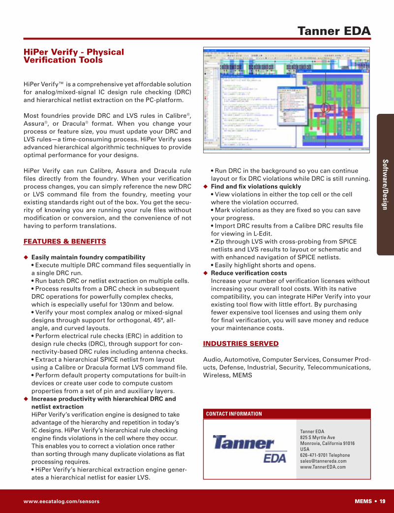
• Run DRC in the background so you can continue layout or fix DRC violations while DRC is still running.
◆ Find and fix violations quickly • View violations in either the top cell or the cell where the violation occurred. • Mark violations as they are fixed so you can save your progress. • Import DRC results from a Calibre DRC results file for viewing in L-Edit.
• Zip through LVS with cross-probing from SPICE netlists and LVS results to layout or schematic and with enhanced navigation of SPICE netlists.
• Easily highlight shorts and opens.◆ Reduce verification costs
Increase your number of verification licenses without increasing your overall tool costs. With its native compatibility, you can integrate HiPer Verify into your existing tool flow with little effort. By purchasing fewer expensive tool licenses and using them only for final verification, you will save money and reduce your maintenance costs.
INDUSTrIeS ServeD
Audio, Automotive, Computer Services, Consumer Prod-ucts, Defense, Industrial, Security, Telecommunications, Wireless, MEMS
HiPer verify - Physical verification Tools
HiPer Verify™ is a comprehensive yet affordable solution for analog/mixed-signal IC design rule checking (DRC) and hierarchical netlist extraction on the PC-platform.
Most foundries provide DRC and LVS rules in Calibre®, Assura®, or Dracula® format. When you change your process or feature size, you must update your DRC and LVS rules—a time-consuming process. HiPer Verify uses advanced hierarchical algorithmic techniques to provide optimal performance for your designs.
HiPer Verify can run Calibre, Assura and Dracula rule files directly from the foundry. When your verification process changes, you can simply reference the new DRC or LVS command file from the foundry, meeting your existing standards right out of the box. You get the secu-rity of knowing you are running your rule files without modification or conversion, and the convenience of not having to perform translations.
FeATUreS & BeNeFITS
◆ Easily maintain foundry compatibility • Execute multiple DRC command files sequentially in a single DRC run. • Run batch DRC or netlist extraction on multiple cells. • Process results from a DRC check in subsequent DRC operations for powerfully complex checks, which is especially useful for 130nm and below. • Verify your most complex analog or mixed-signal designs through support for orthogonal, 45°, all-angle, and curved layouts. • Perform electrical rule checks (ERC) in addition to design rule checks (DRC), through support for con-nectivity-based DRC rules including antenna checks. • Extract a hierarchical SPICE netlist from layout using a Calibre or Dracula format LVS command file. • Perform default property computations for built-in devices or create user code to compute custom properties from a set of pin and auxiliary layers.
◆ Increase productivity with hierarchical DRC and netlist extraction HiPer Verify’s verification engine is designed to take advantage of the hierarchy and repetition in today’s IC designs. HiPer Verify’s hierarchical rule checking engine finds violations in the cell where they occur. This enables you to correct a violation once rather than sorting through many duplicate violations as flat processing requires. • HiPer Verify’s hierarchical extraction engine gener-ates a hierarchical netlist for easier LVS.
Software/D
esignSoft
war
e/D
esig
n

Sensors and MEMS Design Resource Catalog 200920 ��� MEMSMEMS
CONTACT INfOrmATION
Tanner research, Inc. - Tanner eDA
Tanner EDA825 S Myrtle AveMonrovia, CA 91016USA1-877-304-5544 Toll Free626-471-9701 [email protected]
◆ Work in a versatile environment • Import DXF with boundary reconstruction and
export GDSII for mask generation to reuse legacy data. • Create low cost, high resolution transparency MEMS masks with L-Edit’s PostScript mask export.
◆ Features designed just for MEMS • Draw curved geometry and edit it as a curve with
L-Edit’s true curved polygon representation. • Use the built-in manufacturing grid to see in real-time what your curved geometry will look like when approximated for fabrication. • Add fillets easily to geometry to reduce mechanical stress at corners.
SySTeM reqUIreMeNTS
◆ Microsoft® Windows XP, Windows Vista™◆ Intel® Pentium® 4 processor or Pentium 4 equivalent
with SSE support◆ 1280 x 1024 Resolution—True Color (24-bit)◆ 3 button mouse
INDUSTrIeS ServeD
Audio, Automotive, Consumer Products, Defense, Indus-trial, Security, Telecommunications, Wireless MEMS, Sensors
L-edit MeMS
In today’s MEMS design world, integration is more important than ever. To compete in a high-efficiency, high-productivity marketplace, you need a toolset that has proven its ability to accelerate the design cycles of commercially successful projects.
Tanner EDA’s L-Edit™ meets your needs because it is the only tool developed specifically for MEMS and IC design. L-Edit makes integration of MEMS devices with analog/mixed-signal processing circuitry easy with powerful fea-tures that exceed the needs of the most demanding user. This leading MEMS and analog/mixed signal IC design tool for the Windows® and Linux® platforms enables you to get started with minimal training.
Since L-Edit shows clear and dark fields of the masks as opposed to other CAD tools designed for mechanical engineering, you can quickly draw and edit masks and easily view different combination of masks to examine their overlaps and interactions. Using powerful features such as excellent curve support, interactive DRC, boolean operations, object snapping, and alignment, you can work more efficiently to save time and money.
L-Edit gives you greater precision by enabling you to perform complex Boolean and derived layer operations with poly-gons of arbitrary shape and curvature. Perform AND, OR, XOR, Subtract, Grow, and Shrink on groups of objects. This allows you to quickly create entire complex curved shapes for MEMS from just a few easily drawn objects.
FeATUreS & BeNeFITS
◆ Create layout with precision • Perform complete hierarchical physical layout with
all-angle polygons, curved polygons and torii. • Use orthogonal, 45°, all-angle, and curved drawing modes. • Speed drawing and editing by snapping the cursor to object vertices, edges, midpoints, center points, and instances. • Perform one-click horizontal or vertical object alignment, equally space objects, or tile objects horizontally, vertically, or in a 2D array. • Specify a reference point for precision editing operations such as object rotation, flip, move, or instance placement using the base point feature. • Quickly change grid sizes with the Multi-grid tool-bar when switching between MEMS and IC layout.
Software/D
esignSoft
war
e/D
esig
n

www.eecatalog.com/sensors MEMS ��� 21MEMS ��� 21 ��� 21
CONTACT INfOrmATION
Tanner research, Inc. - Tanner eDA
Tanner EDA825 S Myrtle AveMonrovia, CA 91016USA1-877-304-5544 Toll Free626-471-9701 [email protected]
◆ All Angle and Curved Design Rule Checking • Perform checks for minimum spacing or overlap
between objects on various layers. • Support for an unlimited number of width, spacing, surround, enclose, extension, overlap, not exist, and density rules. • High performance boolean and select operations work on all-angled and curved geometry. • Create complex DRC rules that are customized to meet proprietary MEMS fabrication processes. • Perform recommended checks to increase yield. • Display DRC violations in real time while you edit your layout with Interactive DRC, helping you create error-free layouts the first time.
SySTeM reqUIreMeNTS
◆ Microsoft® Windows XP, Windows Vista™◆ Intel® Pentium® 4 processor or Pentium 4 equivalent
with SSE support◆ 1280 x 1024 Resolution—True Color (24-bit)◆ 3 button mouse
APPLICATIoN AreAS
Audio, Automotive, Consumer Products, Defense, Industrial, Security, Telecommunications, Wireless, MEMS, Sensors
L-edit MeMS Design
To make MEMS cost-effective enough for mass produced commercial products, they need to be integrated with analog/mixed signal circuitry, have high yield and have low cost per die. To achieve this goal, you need a toolset that was developed specifically for MEMS and IC design and has the proven capabilities to assist in achieving high yield.
Tanner EDA’s L-Edit™ MEMS Design not only makes integra-tion of MEMS devices with analog/mixed-signal processing circuitry easy but also gives you the tools you need to improve the manufacturability of your MEMS devices. To shorten your design cycle, this leading MEMS and analog/mixed signal IC design tool for the Windows® and Linux® platforms enables you to get started with minimal training.
L-Edit MEMS Design has advanced design rule checking to allow you to easily find design flaws and improve yield. Since most MEMS processes are very specialized or proprietary, you can easily setup rules with its graphical interface, making it configurable for any technology.
To shorten your verification time, L-Edit MEMS Design speeds the process with an advanced Verification Error Navigator that takes you instantly to the location of a viola-tion in the layout editor and provides a clear and thorough summary report of DRC results.
FeATUreS & BeNeFITS
◆ Work in the format that mask shops use. • Import DXF with boundary reconstruction and
export GDSII for mask generation to reuse legacy data. • Avoid confusion and errors on clear and dark field masks when mask shops convert DXF. • Display the clear and dark fields of the masks easily in L-Edit MEMS Design and see in real-time what your curved geometry will look like when approximated for fabrication. • Draw filled polygons for your masks instead of estimating it with zero-width line used by mechanical drafting programs.
◆ UPI and T-Cells • Create parameterized cells called T-Cells™
consisting of user-defined input parameters and layout-generating code to create complex MEMS structures. • Create, place, and align MEMS structures with L-Comp™, a set of high-level composition functions that provide a simple toolkit for creating T-Cell code.
Software/D
esignSoft
war
e/D
esig
n

Sensors and MEMS Design Resource Catalog 200922 ��� MEMSMEMS
CONTACT INfOrmATION
Tanner eDA
Tanner EDA825 S Myrtle AveMonrovia, California 91016USA626-471-9701 [email protected]
◆ Navigate efficiently
• Efficiently traverse design hierarchy with top-down and bottom-up hierarchical view, non-instanced cells view, or view cells sorted by their modified date • Drag and drop cells into layout from library files, other design files, or the current design database • Easily replace instances of one cell with another cell, at the current level or throughout the design
◆ Verify complex designs
• Display violations in real-time while you edit your layout with L-Edit Interactive DRC • Quickly visualize node connectivity with L-Edit Node Highlighting so you can quickly find and fix LVS problems • Generate a SPICE netlist from layout with L-Edit Extract™ for LVS or post-layout simulation
SySTeM reqUIreMeNTS
◆ Microsoft® Windows XP, Windows Vista™◆ Intel® Pentium® 4 processor or Pentium 4 equivalent
with SSE support◆ 1280 x 1024 Resolution—True Color (24-bit)◆ 3 button mouse
INDUSTrIeS ServeD
Audio, Automotive, Consumer Products, Defense, Indus-trial, Security, Telecommunications, Wireless, MEMS
L-edit - Physical Design Tools
In today’s analog design world, speed is more important than ever. To compete in a high-efficiency, high-produc-tivity marketplace, you need a toolset that has proven its ability to accelerate the design cycles of commercially successful projects.
Tanner EDA’s L-Edit™ meets your needs by combining the fastest rendering available with powerful features that exceed the needs of the most demanding user. This leading analog/mixed signal IC design tool for the PC platform enables you to get started with minimal training. You can draw and edit quickly, with fewer keystrokes and mouse clicks than other layout tools. Using powerful features such as interactive DRC, object snapping, and alignment, you can work more efficiently to save time and money.
L-Edit increases your productivity by enabling you to import Cadence® Virtuoso® and Laker™ technology and display files for quick setup. Save time by using foundry-provided files directly, allowing you to avoid having to set up technology information manually. Once you’ve begun using L-Edit, the CAD support burden for your physical design tools will be reduced, enabling you to focus on other mission critical tasks.
FeATUreS & BeNeFITS
◆ Create layout with precision
• Perform complete hierarchical physical layout with all-angle and curved polygons • Perform AND, OR, XOR, Subtract, Grow, and Shrink on groups of objects • Use orthogonal, 45°, all-angle, and curved drawing modes
◆ Use L-Edit Schematic Driven Layout capabilities
• Use netlist files in T-Spice™, HSPICE®, PSpice®, structural Verilog, or CDL formats • Speed layout and routing with cell instances that display highlighted pins, nodes, and flylines
◆ Use parameterized T-Cells
• Create versatile cells that consist of user-defined input parameters and layout-generating code • Extend your T-Cell™ library with L-Edit’s automatic layout to T-Cell generator
Software/D
esignSoft
war
e/D
esig
n

www.eecatalog.com/sensors MEMS ��� 2�MEMS ��� 2� ��� 2�
CONTACT INfOrmATION
Tanner eDA
Tanner EDA825 S Myrtle AveMonrovia, California 91016USA626-471-9701 [email protected]
◆ Work in a faster, easier design environment • Enables easy creation of syntax-correct SPICE through a command wizard. • Highlights SPICE Syntax through a text editor. • Enables you to link from syntax errors to the SPICE deck displays. • Provides “.alter” command for easy what-if simula-tions with netlist changes.
◆ Perform sophisticated analysis Superior numerical techniques to achieve con-vergence on circuits that are often impossible to simulate with other SPICE programs. • DC and AC analysis. • Transient analysis with Gear or trapezoidal integration. • Enhanced noise analysis. • Monte Carlo analysis over unlimited variables and trials with device and lot variations. • Virtual measurements with functions for timing, error, and statistical analysis. • Parameter sweeping using linear, log, discrete value, or external file data sweeps.
◆ With T-Spice, you can: • Optimize designs with variables and multiple constraints by applying a Levenberg-Marquardt non-linear optimizer. • Use plot statements that support wildcards. • Use plot statements and parameter definitions that support mathematical expressions involving C-style math functions. • Use bit and bus logic waveform inputs.
INDUSTrIeS ServeD
Audio, Automotive, Consumer Products, Defense, Indus-trial, Security, Telecommunications, Wireless, MEMS
T-Spice - Analog Simulation Tools
T-Spice is a complete design capture and simulation solution that provides accuracy and convergence with market-proven reliability.
To transform your ideas into designs, you must be able to simulate large circuits quickly and with a high degree of accuracy. That means you need a simulation tool that offers fast run times, integrates with your other design tools, and is compatible with industry standards.
Tanner T-Spice™ Circuit Simulator puts you in control of simulation jobs with an easy-to-use graphical inter-face and a faster, more intuitive design environment. With key features such as multi-threading support, device state plotting, real-time waveform viewing and analysis, and a command wizard for simpler SPICE syntax creation, T-Spice saves you time and money during the simulation phase of your design flow.
T-Spice enables more accurate simulations by supporting the latest transistor models—including BSIM4 and the Penn State Philips (PSP) model. Given that T-Spice is compatible with a wide range of design solutions and runs on PC-based systems, it fits easily and cost-effec-tively into your current tool flow.
FeATUreS & BeNeFITS
◆ Improve simulation accuracy with advanced modeling features
• Supports Verilog-A for analog behavioral modeling, allowing designers to prove system level designs before doing full device level design and easily create custom compact models for special devices.
• Supports foundry extensions, including HSPICE® foundry extensions to models.
• Supports PSP, BSIM3.3, BSIM4.5, BSIM SOI 4.0, EKV 2.6, MOS 9, 11, 20, 30, 31, 40, RPI a-Si & Poly-Si TFT, VBIC, Modella, and MEXTRAM models. • Includes two stress effect models, from the Berke-ley BSIM4 model and from TSMC processes, in the BSIM3 model to provide more accuracy in smaller geometry processes. • Performs non-quasi-static (NQS) modeling. • Supports comprehensive geometry-based parasitic models for multi-finger devices. • Models partially depleted, fully depleted, and uni-fied FD-PD SOI devices. • Models self-heating and RF resistor networks.
• Perform Safe Operating Area checks to create robust designs.
Software/D
esignSoft
war
e/D
esig
n

Sensors and MEMS Design Resource Catalog 20092� ��� Data AcquisitionData Acquisition
CONTACT INfOrmATION
Microchip Technology Inc.
Microchip Technology Inc.2355 W. Chandler Blvd.Chandler, AZ 85224USA888-MCU-MCHP Toll Free480-792-7200 Telephone480-792-7277 [email protected]
AvAILABILITy
Now. For further information, contact any Microchip sales representative or authorized worldwide distributor, or visit Microchip’s Web site at http://www.microchip.com.
APPLICATIoN AreAS
The PIC24FJ64GA004 family is designed to meet a wide range of design engineering needs across a broad spectrum of industries. Specific application examples include: consumer (security systems, heating control, audio equipment); automotive (body control, steering systems); instrumentation/measurement (scales, medical instruments and monitoring); industrial (building monitor-and-control systems, security/access systems, sensors).
World’s First 16-bit Microcontrollers With 64 Kbytes of Flash in 28-pin PackagesSupported 16-bit Architectures: PIC® Microcontrollers
With the PIC24FJ64GA004 16-bit microcontroller family, Microchip Technology extends its 16-bit portfolio by providing smaller and lower cost 28- and 44-pin pack-ages with 16 to 64 Kbytes of Flash program memory and up to 8 Kbytes of RAM. The PIC24FJ64GA002 micro-controller provides more onboard memory than any other 28-pin packaged 16-bit microcontroller. The entire PIC24FJ64GA004 family allows the flexible use of all onboard peripherals, by enabling designers to map them to the pin they desire through the “Peripheral Pin Select” pin-mapping function.
Design engineers are adding functions in software to even the smallest microcontrollers, driving the demand for higher performance and larger memory in low pin count packages—to better address cost- and space-con-strained applications. The PIC24FJ64GA004 family’s industry-leading memory densities, in packages as small as a 6x6 mm QFN, address these design concerns.
However, engineers still require a broad range of periph-eral combinations within these low pin count packages. The PIC24FJ64GA004 family contains a similar periph-eral set to the 100-pin PIC24FJ128GA family, in a package as small as 28 pins. Through Peripheral Pin Select, Microchip enables designers to use the available pins in the exact manner they like. This flexibility provides engineers with the option to use a smaller, more cost-effective microcontroller.
The PIC24FJ64GA004 family is designed to meet a wide range of design engineering needs across a broad spec-trum of industries.
FeATUreS & BeNeFITS
◆ Two independent channels of I2C™, UART and SPI communications, enabling communications to a number of devices over multiple protocols, for easier system design.
◆ Designed for an easy transition to other members in the PIC24F family and for migration to other families in Microchip’s 16-bit portfolio, including the PIC24H and dsPIC33 families, through code compatibility.
microcontrollers
mic
roco
ntro
llers
and
Cor
es
Note: The Microchip name and logo, PIC, and MPLAB are registered trade-marks of Microchip Technology Inc. in the USA and other countries. All other trademarks mentioned herein are the property of their respective companies.

www.eecatalog.com/sensors Data Acquisition ��� 2�Data Acquisition ��� 2� ��� 2�
CONTACT INfOrmATION
Silicon Laboratories
Silicon Laboratories400 W Cesar ChavezAustin, TX 78701USA(877) 444-3032 Toll [email protected]/mcu
TeCHNICAL SPeCS
◆ Precision internal oscillators: 24.5 MHz with ±2% accuracy supports UART operation; spread-spectrum mode for reduced EMI
◆ Ultra-Small Package • 24-pin QFN (4x4 mm)◆ Temperature Range: –40 to +85 °C◆ On-chip debug circuitry facilitates full speed, non-
intrusive in-system debug (no emulator required)
AvAILABILITy
Available Now in QFN35, QFN24, LQFP32 packages
APPLICATIoN AreAS
Portable Personal Medical Products, Remote Controls, Portable Audio, Consumer Electronics, Wireless Sensors and Security, Wireless Meter Reading, Industrial Moni-toring and Control
Low Power Mixed-signal 8-bit MCUsSupported Operating Systems: 8051
Supported 8-bit Architectures: 8-bit, 8051
The C8051F9xx MCU family is capable of full-spec oper-ation down to 0.9 V and up to 3.6 V, enabling single-cell battery operation as well as dramatically increased bat-tery life for dual-cell applications. With an integrated dc-dc converter, the C8051F9xx has been designed to provide a fast wake-up time, low active-mode, and ultra-low sleep mode current consumptions.
Best-in-Class ToolsSilicon Labs delivers industry-leading tools to help speed design and accelerate market entry. The com-plete, low-cost professional development kits include everything required to immediately begin system design including IDE, target board, cables, and power supply. An inexpensive ToolStick Daughter Card and Base Adapter also provide a full development envi-ronment. www.silabs.com/toolstick
FeATUreS & BeNeFITS
◆ One-cell mode 0.9–1.8 V, two-cell mode 1.8–3.6 V. Built-in dc-dc converter with 1.8 –3.3 V output can supply external devices. Retains state and RAM contents over full supply range; fast wakeup.
◆ 10-Bit ADC with up to 300 ksps, up to 15 external inputs, external pin or internal VREF (no external capacitor required), built-in temp sensor. Two Comparators, low current. Up to 15 Capacitive Touch Sense inputs
◆ High-Speed 8051 25MHz Single Cycle Core • Pipe-lined instruction architecture; executes
70% of instructions in 1 or 2 system clocks • 25 MIPS peak throughput with 25 MHz clock • Expanded interrupt handler◆ Digital Peripherals • 16 port I/O; All 5 V tolerant with programmable
drive strength • Hardware enhanced UART, SPI and SMBus™
serial ports available concurrently • Low power 32-bit smaRTClock (0.5 uA) operates
down to 0.9V◆ 4352 bytes internal data RAM (256 + 4K) • 64 kB bytes Flash; In-system programmable in
1024-byte sectors; Full read/write/erase func-tionality over the entiresupply range
microcontrollers and Coresm
icro
cont
rolle
rs a
nd C
ores

Sensors and MEMS Design Resource Catalog 200926 ��� Data AcquisitionData Acquisition
CONTACT INfOrmATION
Perpetuum Ltd
Perpetuum LtdEpsilon HouseSouthampton Science ParkSouthampton SO16 7NP United Kingdom+44-2380-765-888 Telephonewww.perpetuum.com
PMG37 Compatible Operating Systems: Any Wireless System
Supported Architecture: Any
The PMG37 energy harvester converts unused mechan-ical vibration into usable electrical energy to power complete wireless sensor systems, eliminating the need for batteries. Generating continuous power these devices can provide enteirely maintenance-free operation of wireless sensors. Optimized to give the highest power output on typical low frequency vibration on rail cars or industrial machines they operate over the full industrial temperature range. The PMG37 is built to withstand the demanding environments found in rail, heavy transpor-tation and industrial facilities
FeATUreS & BeNeFITS
◆ 20+ mW of power generation above 0.25g RMS and 40+ mW of power generation above 0.50 g RMS
◆ Tuned vibration harvester for low frequency vibra-tions associated with rail and tractor trailors
◆ Output Voltage up to 10V◆ 20+ year life◆ Wide operating temperature range, -40C to +85C
AvAILABILITy
Stock to 6 weeks
APPLICATIoN AreAS
Wireless condition monitoring, asset tracking and loca-tion
modulesm
odul
es


Paying through the nosefor your EDA tools?
© 2009 Tanner Research. All rights reserved. Speeding Concept to Silicon
Corporate Headquarters825 South Myrtle AvenueMonrovia, CA 91016-3424 USATel: +1-626-471-9700Toll Free: 877-325-2223Fax: +1-626-471-9800Email: [email protected]: www.tannereda.com
Tanner EDA, #1 in analog mixed-signal IC designTo learn more go to www.TannerEDA.com or call +1 626-471-9701.Going to DAC? Stop by at booth #3655.
Find out why 25,000 engineers worldwide useTanner EDA, the affordable high-performance solution.
SCHEMATICCAPTURE
PHYSICALLAYOUT
PHYSICALVERIFICATION
PARASITICEXTRACTION
ANALOGSIMULATION
S-Edit™ L-Edit™ HiPer Verify™ HiPer PX™T-Spice™
Verilog-A