self-assembly of molecules on silicon: theoretical approaches
TRANSCRIPT
Fabrizio [email protected]
Institut d’Electronique, Micro-électronique et Nanotechnologie (IEMN-CNRS), Université des Sciences et Technologies de Lille,
Villeneuve d’Ascq (France)
Self-Assembly of Molecules on Silicon:Theoretical Approaches

OUTLINE
1. A few ideas around molecules on semiconductors
2. Building blocks for computer simulation: ab initio modelling of alkyl molecules covalently bonded to Si surfaces
3. Structural and electronic properties of an organic / inorganic semiconductor interface
4. Classical molecular dynamics of molecular monolayers deposited on semiconductor surfaces
5. Physisorption of supramolecular structures on semiconductor surfaces
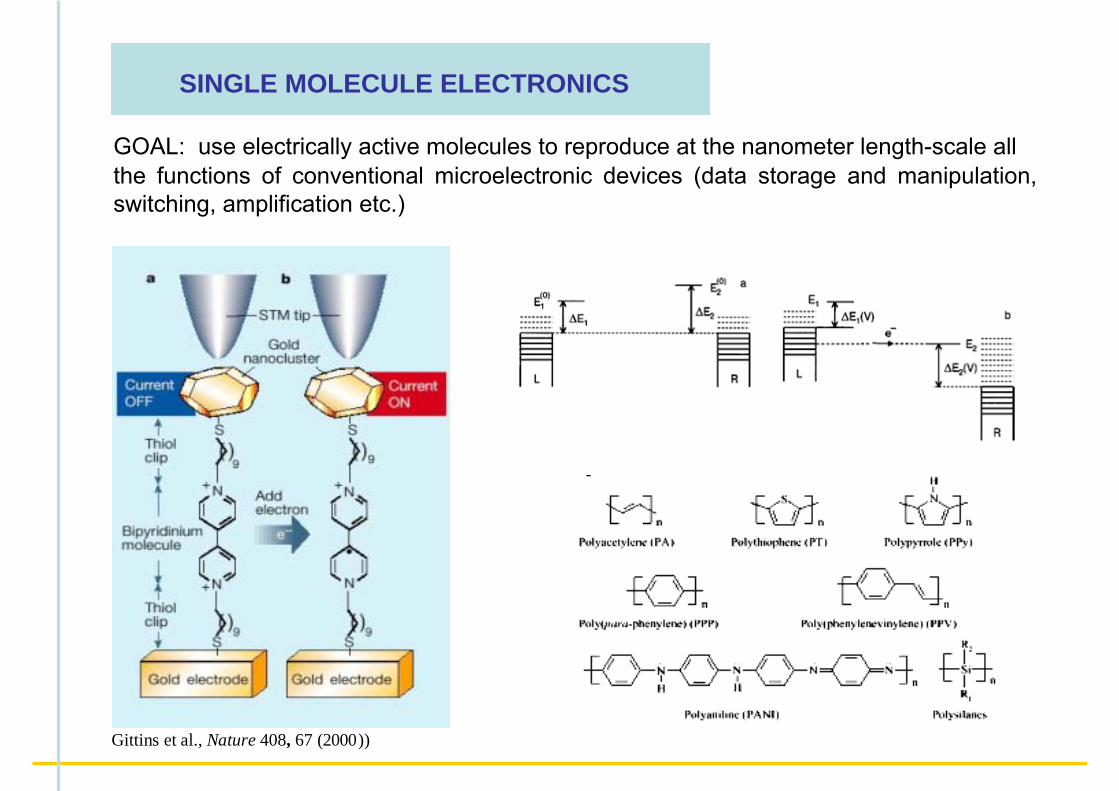
SINGLE MOLECULE ELECTRONICS
GOAL: use electrically active molecules to reproduce at the nanometer length-scale all the functions of conventional microelectronic devices (data storage and manipulation, switching, amplification etc.)
Gittins et al., Nature 408, 67 (2000))

A MOLECULAR MEMORY CELL
Red-ox center made of 3 benzenic rings, the central element being activated by the presence of NO2 and NH2 side groups.
Upon increasing voltage, the initial configuration (A) is reduced to a conducting state (B) or twice reduced to an insulating state (C ).
When the voltage is removed the molecule goes back to (A) with much shorter commuting times than ordinary solid-state devices.
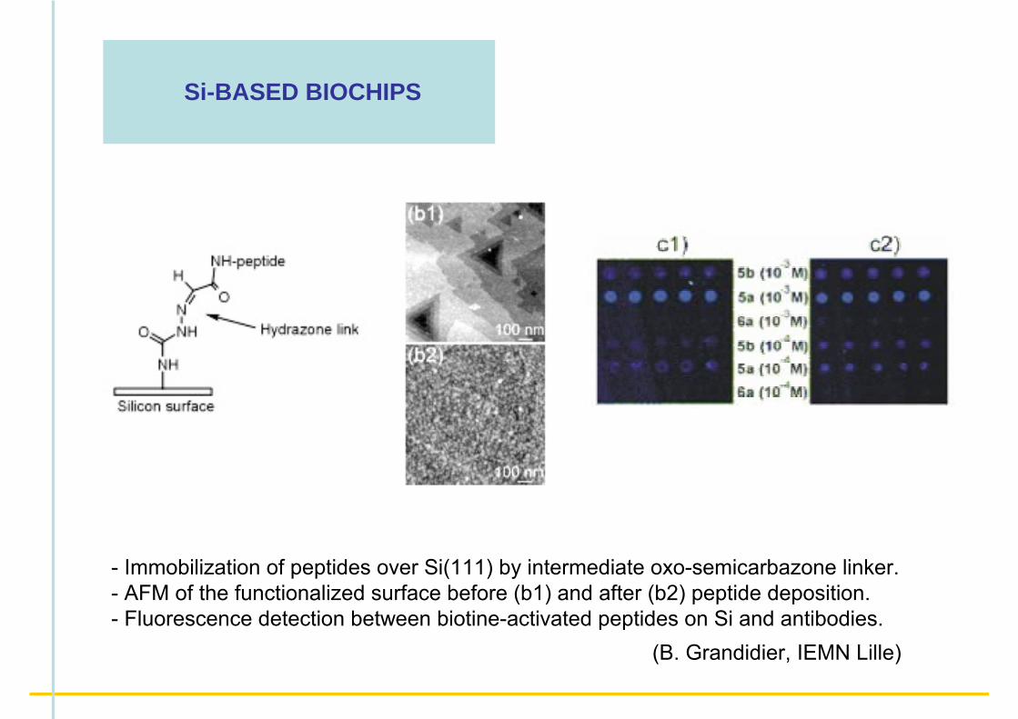
- Immobilization of peptides over Si(111) by intermediate oxo-semicarbazone linker. - AFM of the functionalized surface before (b1) and after (b2) peptide deposition.- Fluorescence detection between biotine-activated peptides on Si and antibodies.
(B. Grandidier, IEMN Lille)
Si-BASED BIOCHIPS
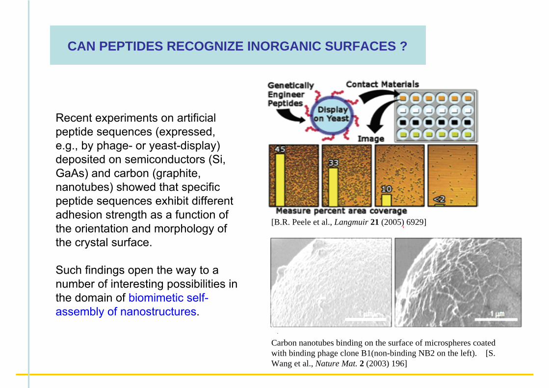
CAN PEPTIDES RECOGNIZE INORGANIC SURFACES ?
Recent experiments on artificial peptide sequences (expressed, e.g., by phage- or yeast-display) deposited on semiconductors (Si, GaAs) and carbon (graphite, nanotubes) showed that specific peptide sequences exhibit different adhesion strength as a function of the orientation and morphology of the crystal surface.
Such findings open the way to a number of interesting possibilities in the domain of biomimetic self-assembly of nanostructures.
Carbon nanotubes binding on the surface of microspheres coated with binding phage clone B1(non-binding NB2 on the left). [S. Wang et al., Nature Mat. 2 (2003) 196]
[B.R. Peele et al., Langmuir 21 (2005) 6929]

DEVICES BASED ON MOLECULAR MONOLAYERS
Sandwich a σ−π chain between a substrate ofSi (n-doped) and a metal contact (Al, Au)
CURRENT RECTIFICATIONIN MOLECULAR MONOLAYERS
D. Vuillaume et al.IEMN Lille

A MOLECULAR DIODE
Formed by an insulating σ-bonded alkyl chain (CH2)n + a “head” with delocalized π-electrons, e.g., phenyl, tiophene, polypirrole, phtalocyanine, etc.
H3Si(CH2)8COO-CH2(1,phenyl)
A dense monolayer of such molecules is grown onto a semiconducting Si substrate, and is subsequently contacted by an Al or Au electrode.
- What is the detailed structure of the Si / σ−π / metal interfaces ?- What is the behavior of energy bands & electrostatic potential in the sandwich ?
- How are the molecular levels modified and readjusted ?

THEORETICAL MODELLING STEPS - 1 (DFT-GGA + plane waves + pseudopotentials, Abinit/CPMD codes)
1) Free molecule (relaxation and energy levels)
2) 2-D packing of the free molecules
3) Covalent bonding between molecule and surface
4) Contact between monolayer and Si(100)
5) LDOS and energy bands(levels) scheme
6) Build top contact with Al (100) slab (open-circuit simulation)
7) New LDOS and energy bands(levels) scheme
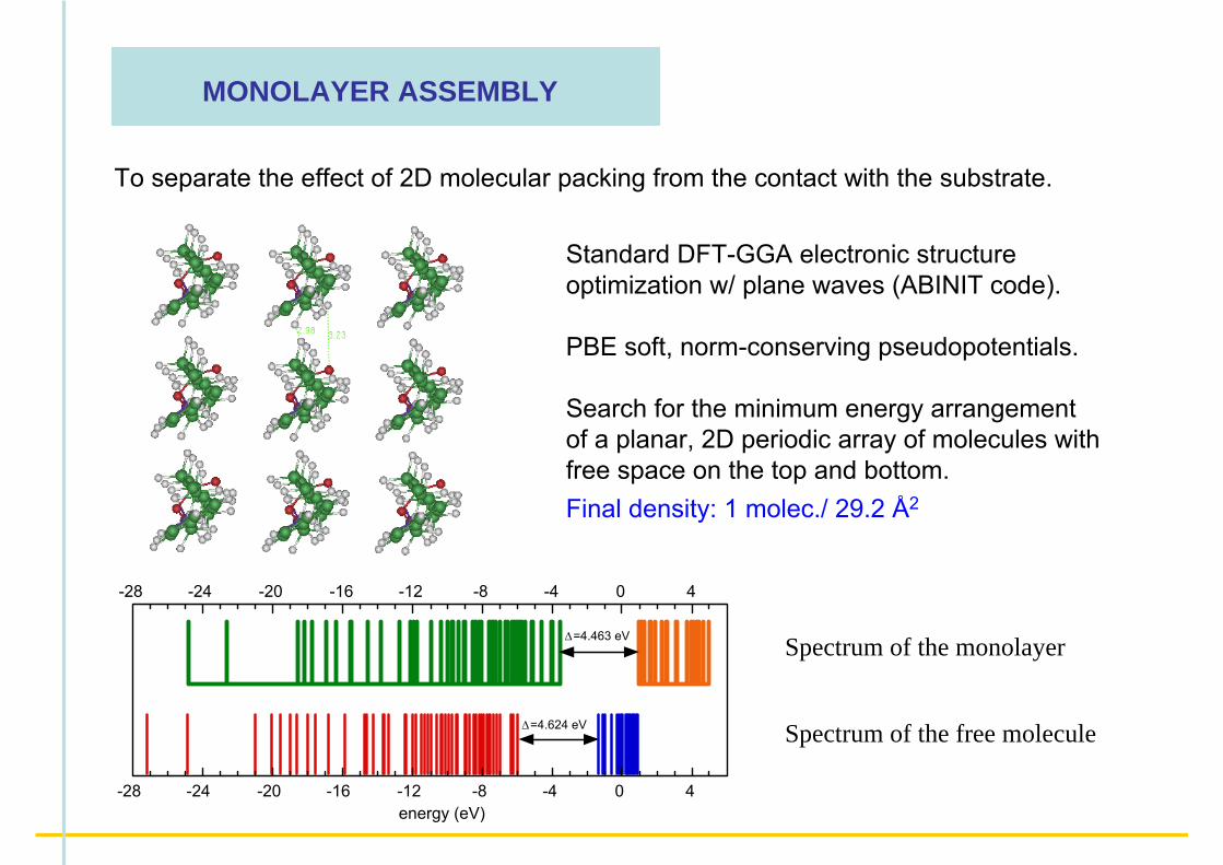
MONOLAYER ASSEMBLY
To separate the effect of 2D molecular packing from the contact with the substrate.
-28 -24 -20 -16 -12 -8 -4 0 4
-28 -24 -20 -16 -12 -8 -4 0 4
energy (eV)
Δ=4.624 eV
Δ=4.463 eV Spectrum of the monolayer
Spectrum of the free molecule
Standard DFT-GGA electronic structure optimization w/ plane waves (ABINIT code).
PBE soft, norm-conserving pseudopotentials.
Search for the minimum energy arrangement of a planar, 2D periodic array of molecules with free space on the top and bottom.Final density: 1 molec./ 29.2 Å2
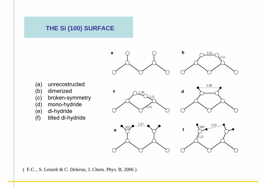
THE Si (100) SURFACE
(a) unrecostructed(b) dimerized(c) broken-symmetry(d) mono-hydride(e) di-hydride(f) tilted di-hydride
( F.C. , S. Letardi & C. Delerue, J. Chem. Phys. B, 2006 )
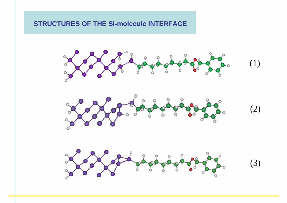
STRUCTURES OF THE Si-molecule INTERFACE
(1)
(2)
(3)

Different surface bonding configurations are observed as a function of the H chemical potential μ (for a fixed μch of the adsorbed alkyl chain)
( F.C. , S. Letardi & C. Delerue, J. Phys. Chem. B, 2006 )
Si-molecule INTERFACE BONDING STRUCTURE
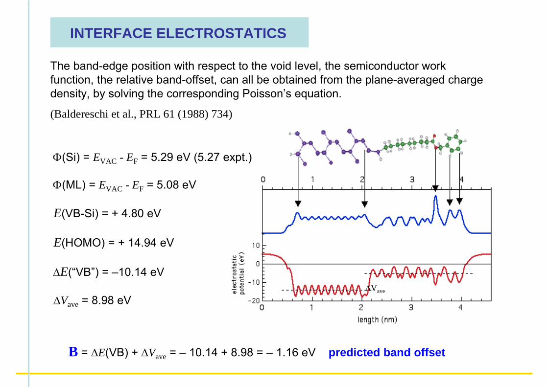
INTERFACE ELECTROSTATICS
The band-edge position with respect to the void level, the semiconductor work function, the relative band-offset, can all be obtained from the plane-averaged charge density, by solving the corresponding Poisson’s equation.
(Baldereschi et al., PRL 61 (1988) 734)
Φ(Si) = EVAC - EF = 5.29 eV (5.27 expt.)
Φ(ML) = EVAC - EF = 5.08 eV
E(VB-Si) = + 4.80 eV
E(HOMO) = + 14.94 eV
ΔE(“VB”) = –10.14 eV
ΔVave = 8.98 eV
B = ΔE(VB) + ΔVave = – 10.14 + 8.98 = – 1.16 eV predicted band offset
ΔVave
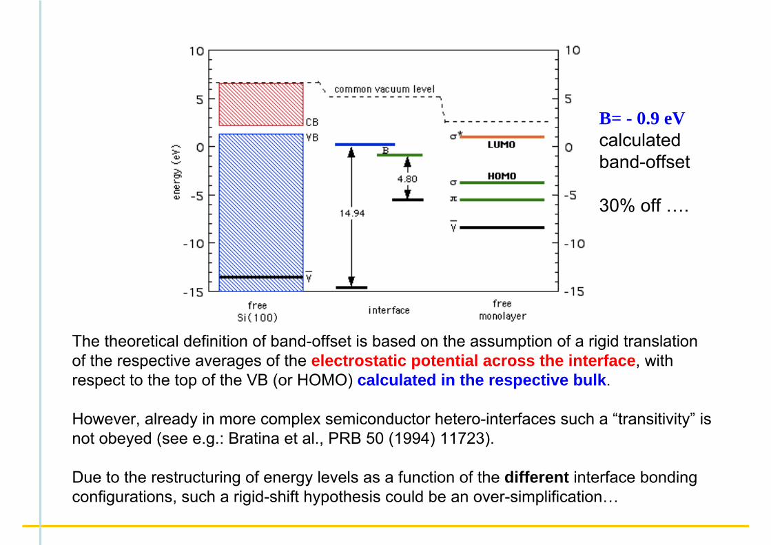
The theoretical definition of band-offset is based on the assumption of a rigid translation of the respective averages of the electrostatic potential across the interface, with respect to the top of the VB (or HOMO) calculated in the respective bulk.
However, already in more complex semiconductor hetero-interfaces such a “transitivity” is not obeyed (see e.g.: Bratina et al., PRB 50 (1994) 11723).
Due to the restructuring of energy levels as a function of the different interface bonding configurations, such a rigid-shift hypothesis could be an over-simplification…
B= - 0.9 eVcalculatedband-offset
30% off ….

Al contact
σ alkyl chain
Si(100) substrate
Benzyl head, orDioxy-benzene
-2 0 2 4 6E (eV)
Al
Si
C
C
σ
π
-1 0 1 2 3 4 5 6 7E (eV)
Al
Si
C
C
σ
π
Block-projected LDOS
Benz
Dioxy
B?
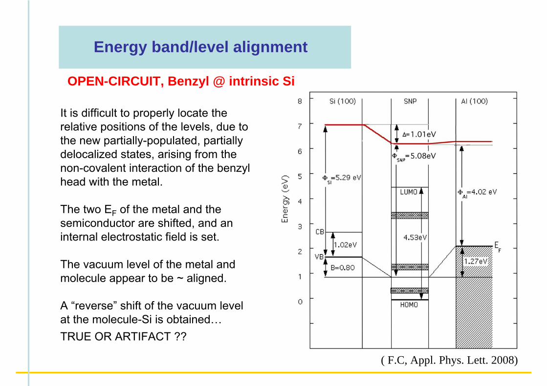
Energy band/level alignment
OPEN-CIRCUIT, Benzyl @ intrinsic Si
It is difficult to properly locate the relative positions of the levels, due to the new partially-populated, partially delocalized states, arising from the non-covalent interaction of the benzyl head with the metal.
The two EF of the metal and the semiconductor are shifted, and an internal electrostatic field is set.
The vacuum level of the metal and molecule appear to be ~ aligned.
A “reverse” shift of the vacuum level at the molecule-Si is obtained…TRUE OR ARTIFACT ??
( F.C, Appl. Phys. Lett. 2008)

THEORETICAL MODELLING STEPS - 2 (empirical MD + CHARMM force field + SW crystal Si pot.)
1) Interpolate surface-molecule covalent bonding parameters from ab initio
2) Build dense monolayer on Si (100) and (111) for differenthead groups
3) {NVT} molecular dynamics at different surface coverages
4) Study essential dynamics of molecules (not eigenmode analysis)
ANTHRACENE
C1
C1
BENZENE
H3
C1
H3
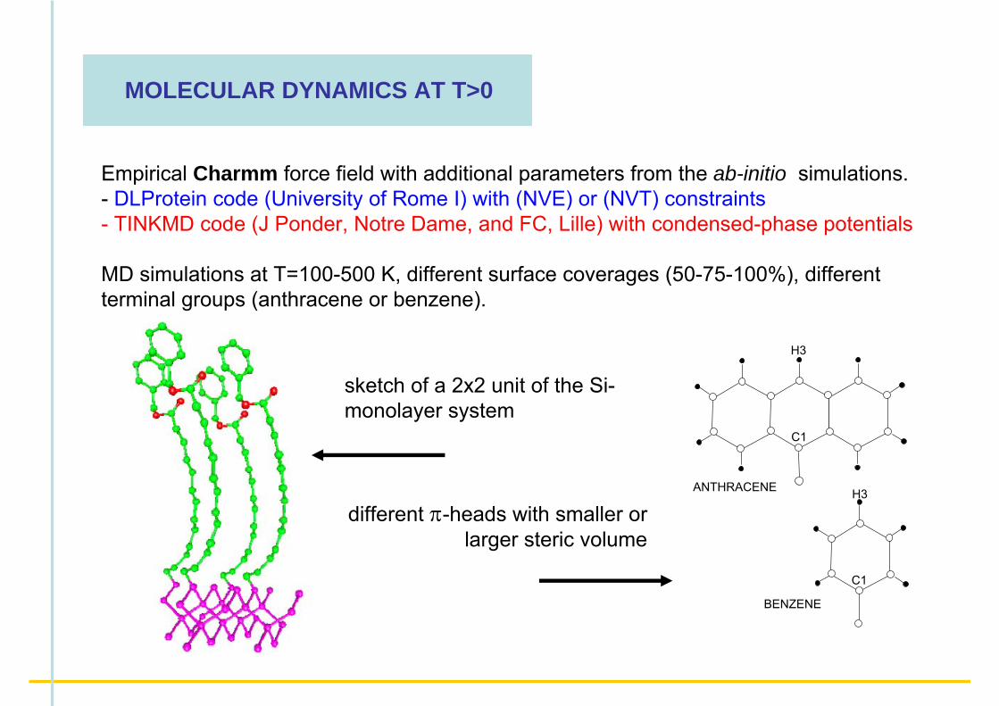
MOLECULAR DYNAMICS AT T>0
sketch of a 2x2 unit of the Si-monolayer system
different π-heads with smaller or larger steric volume
Empirical Charmm force field with additional parameters from the ab-initio simulations.- DLProtein code (University of Rome I) with (NVE) or (NVT) constraints- TINKMD code (J Ponder, Notre Dame, and FC, Lille) with condensed-phase potentials
MD simulations at T=100-500 K, different surface coverages (50-75-100%), different terminal groups (anthracene or benzene).
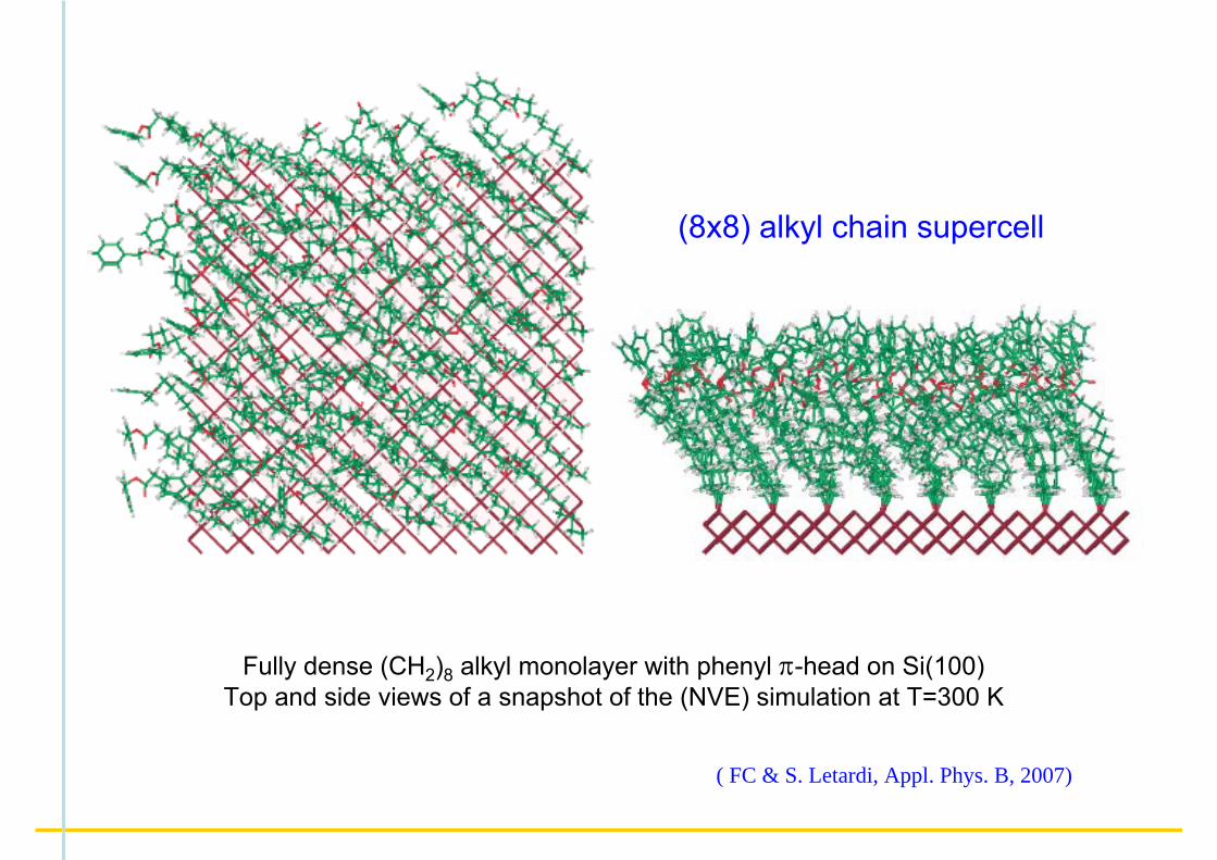
Fully dense (CH2)8 alkyl monolayer with phenyl π-head on Si(100)Top and side views of a snapshot of the (NVE) simulation at T=300 K
(8x8) alkyl chain supercell
( FC & S. Letardi, Appl. Phys. B, 2007)

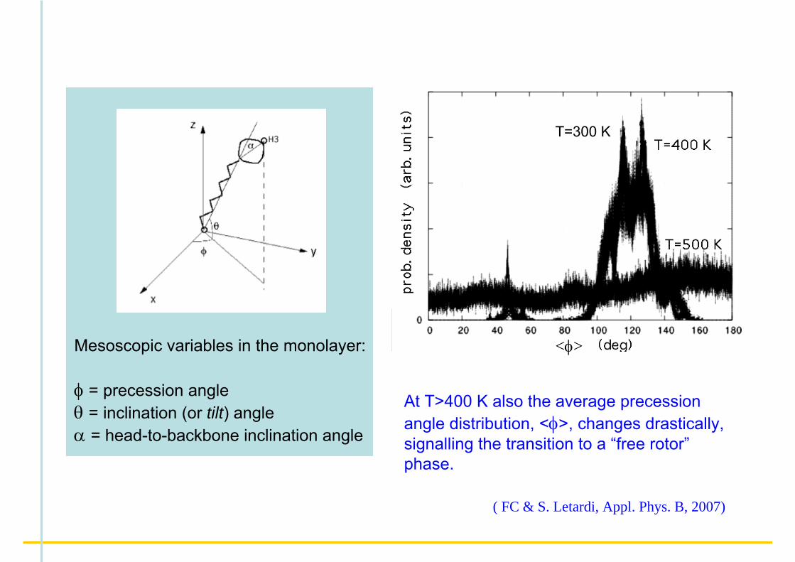
Mesoscopic variables in the monolayer:
φ = precession angleθ = inclination (or tilt) angleα = head-to-backbone inclination angle
MD time (~2x10⁻³ ps)
ESSENTIALDYNAMICS

Mesoscopic variables in the monolayer:
φ = precession angleθ = inclination (or tilt) angleα = head-to-backbone inclination angle
A = anthracene headB = benzene head
Upon increasing temperature, the molecules in the monolayer become more and more perpendicular to the substrate, with a rather sharp transition above T~400 K.
Mesoscopic variables in the monolayer:
φ = precession angleθ = inclination (or tilt) angleα = head-to-backbone inclination angle
T=300 K
<φ>
At T>400 K also the average precession angle distribution, <φ>, changes drastically, signalling the transition to a “free rotor”phase.
( FC & S. Letardi, Appl. Phys. B, 2007)
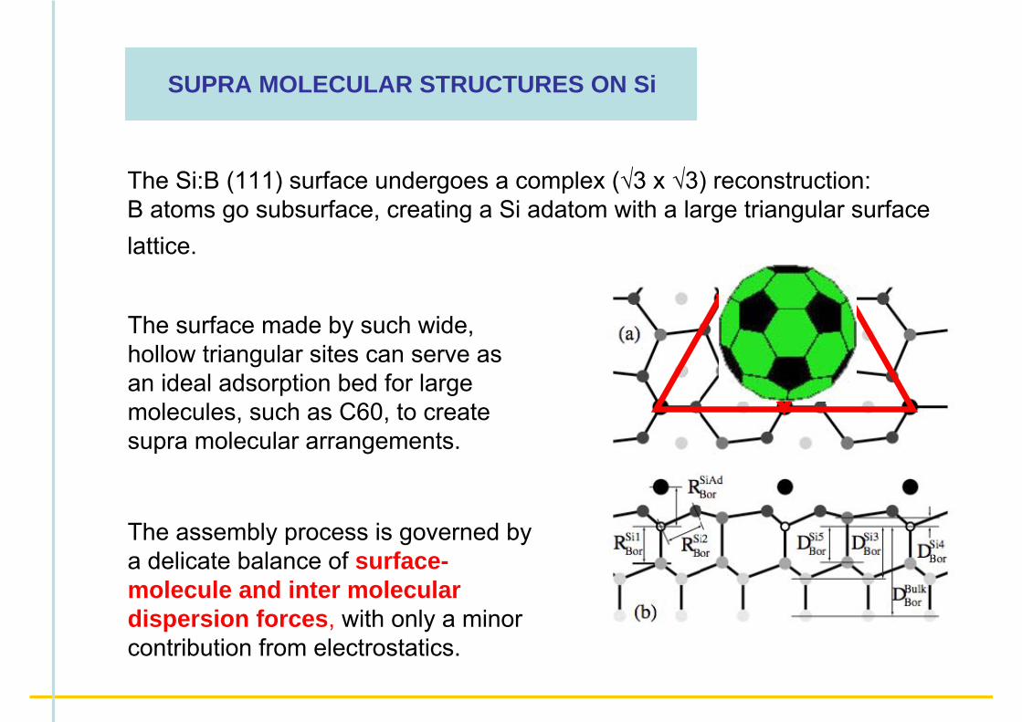
The Si:B (111) surface undergoes a complex (√3 x √3) reconstruction:B atoms go subsurface, creating a Si adatom with a large triangular surface lattice.
The surface made by such wide, hollow triangular sites can serve as an ideal adsorption bed for large molecules, such as C60, to create supra molecular arrangements.
SUPRA MOLECULAR STRUCTURES ON Si
The assembly process is governed by a delicate balance of surface-molecule and inter molecular dispersion forces, with only a minor contribution from electrostatics.

Experimentally, C60 on the pure Si(111) surface (7x7 reconstructed) has a strong interaction with Si dangling bonds and does not form regular super structures, unless a second-layer is grown.
On the Si:B(111) surface, C60 organizes in regular structures, growing from surface defects (steps, twins).
A regular hexagonal pattern is observed at the highest coverage density.
At lower density, less regular patterns are observed both in pure and B-doped (111) surfaces.
(T. Stimpel et al., Mat. Sci. Eng. B 89 (2002) 394)
THEORETICAL MODELLING STEPS - 3 (MM3 force field + SW crystal Si pot. + Kinetic Monte Carlo)
1) Role of Van der Waals forces in physisorption of molecular aggregates on surfaces (NOTE: VdW cannot yet be calculated fully ab-initio !)
1) Build monolayers of C-60 on Si:B(111) at different coverages
3) Run MD simulations with empirical Van der Waals forces
4) Model large scale and long time evolution of the system by Kinetic Monte Carlo

MOLECULAR DYNAMICS ON Si:B(111)
MD with Stilliger-Weber forces for Si and B atoms (plus constraints).C-60 described by the molecular force field MM3, with empirical Van der Waals forces:
VVDW (R) = ε σR
⎛ ⎝ ⎜
⎞ ⎠ ⎟
12
−σR
⎛ ⎝ ⎜
⎞ ⎠ ⎟
6⎡
⎣ ⎢
⎤
⎦ ⎥ σ,ε additive (Berthelot)
atom-dependent parameters
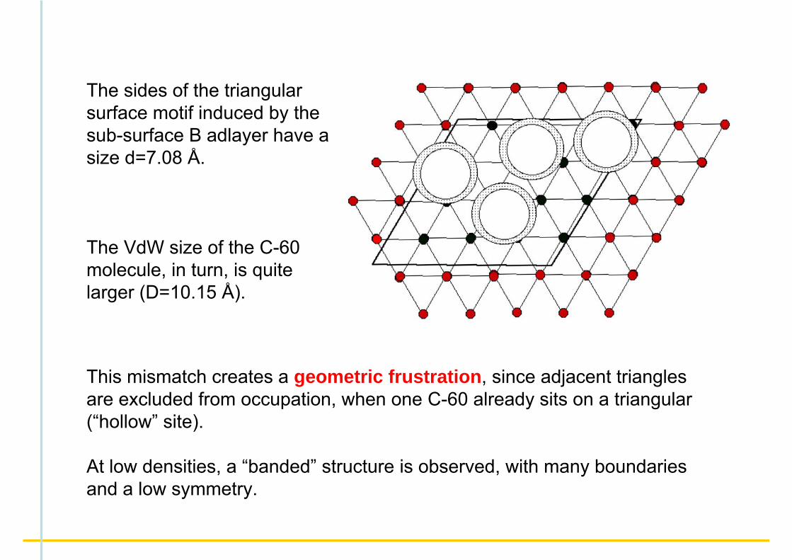
The sides of the triangular surface motif induced by the sub-surface B adlayer have a size d=7.08 Å.
The VdW size of the C-60 molecule, in turn, is quite larger (D=10.15 Å).
This mismatch creates a geometric frustration, since adjacent triangles are excluded from occupation, when one C-60 already sits on a triangular (“hollow” site).
At low densities, a “banded” structure is observed, with many boundaries and a low symmetry.

Upon increasing the density, the C-60 have to overcome the frustration by choosing other occupation schemes.
One possibility suggested by MD simulations at increasing coverage is that some molecules occupy a “top” site, by sitting over a Si adatom.
This is a trade-off between the increase in intermolecular interactions (6 neighbors instead of 3) and the decrease in surface interaction.
QuickTime™ e undecompressore TIFF (Non compresso)
sono necessari per visualizzare quest'immagine.
QuickTime™ e undecompressore TIFF (Non compresso)
sono necessari per visualizzare quest'immagine.
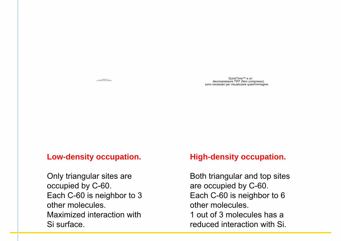
Low-density occupation.
Only triangular sites are occupied by C-60.Each C-60 is neighbor to 3 other molecules.Maximized interaction with Si surface.
High-density occupation.
Both triangular and top sites are occupied by C-60.Each C-60 is neighbor to 6 other molecules.1 out of 3 molecules has a reduced interaction with Si.

Kinetic Monte Carlo model of C60 on Si:B(111)
We use a fixed lattice with the symmetry of Si:B(111) surface. Site-occupation constraints are used to mimick the geometric constraints.
Site-site and site-surface interactions are described by a Ising hamiltonian:
Hij = α ijμiμ j + βj
∑ μi , μi=0,1
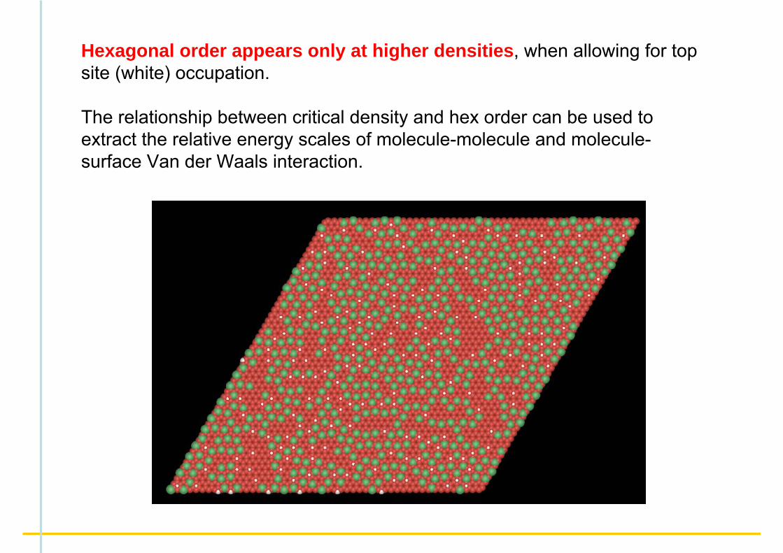
Hexagonal order appears only at higher densities, when allowing for top site (white) occupation.
The relationship between critical density and hex order can be used to extract the relative energy scales of molecule-molecule and molecule-surface Van der Waals interaction.

CONCLUSIONS
1. The structure of the molecule-semiconductor interface is a fundamental variable that determines many properties of the final device.
2. Electronic structure calculations supply the input structures and data to empirical molecular dynamics simulations. This coupling can elucidate the synthesis conditions of nanoscale molecular devices.
3. Molecular packing in the monolayer has a strong effect on both the electronic structure and interface electrostatics. A monolayer contacted to a semiconductor has additional constraints w/r to the free molecule.
4. The surface structure of the adsorbed monolayer exhibits stronginterplay between thermodynamic constraints and active degrees of freedom, e.g. internal rotation, libration and oscillations.
5. Non-covalent dispersion forces play a relevant role in supramolecular ordering transitions in 2Dim on semiconductor surfaces.
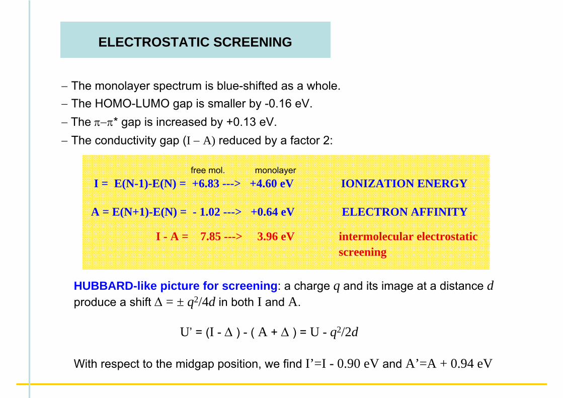
ELECTROSTATIC SCREENING
− The monolayer spectrum is blue-shifted as a whole.− The HOMO-LUMO gap is smaller by -0.16 eV.− The π−π* gap is increased by +0.13 eV.− The conductivity gap (I − A) reduced by a factor 2:
free mol. monolayerI = E(N-1)-E(N) = +6.83 ---> +4.60 eV IONIZATION ENERGY
A = E(N+1)-E(N) = - 1.02 ---> +0.64 eV ELECTRON AFFINITY
I - A = 7.85 ---> 3.96 eV intermolecular electrostatic screening
HUBBARD-like picture for screening: a charge q and its image at a distance dproduce a shift Δ = ± q2/4d in both I and A.
U’ = (I - Δ ) - ( A + Δ ) = U - q2/2d
With respect to the midgap position, we find I’=I - 0.90 eV and A’=A + 0.94 eV
A FEW CONCLUSIONS FROM THE ab initio MODEL
1) Si/molecule/metal constitute a significant test bed. Several interface bonding states may contribute, depending on local stoichiometry, and surface energetics. The atomic details of bonding influence heavily the energy level diagram.
2) Dense molecular packing leads to a sizeable electrostatic screening, changing the electron affinity (A) and ionization energy (I) of the free molecule: the nature of the gap states is changed, the conductivity gap I-A can be reduced by a large factor.
3) Band-offset is classically defined in terms of a rigid translation of the bands. In view of the complex rearrangement of the energy levels at the interface formation, this is probably an oversimplification.
4) Some arbitrariness is involved in assigning the band offset and vacuum levels of the multiple interface, for the open-circuit configuration. Polarization, and shift in the relative vacuum levels is obtained at the semiconductor-molecule interface.
5) Based on such observations, the analogy with heterogeneous semiconductors can be regarded only as qualitative and approximate.


SURFACE BONDING, ab initio MD
Monolayer of CH3-CH2-SiH3 on Si(100), density 1.7x10⁻² Å-2 (~ experimental dens.)Single-bond molecule-surface + dangling bonds saturated with H
- surface stress induces a strong distortion/reconstruction of the surface- this, in turn, gives rise to surface-localized electron states (→ e-h traps)
start after ~10 psec
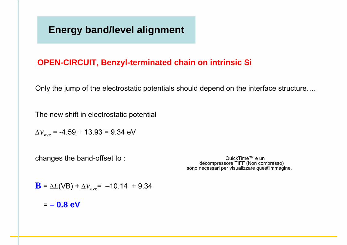
Energy band/level alignment
OPEN-CIRCUIT, Benzyl-terminated chain on intrinsic Si
QuickTime™ e undecompressore TIFF (Non compresso)
sono necessari per visualizzare quest'immagine.
Only the jump of the electrostatic potentials should depend on the interface structure….
The new shift in electrostatic potential
ΔVave = -4.59 + 13.93 = 9.34 eV
changes the band-offset to :
B = ΔE(VB) + ΔVave= –10.14 + 9.34
= – 0.8 eV

Building of the interface between Si and the monolayer implies a substantial rearrangement of the molecular levels :
- the HOMO splits into σ and π levels, at about EF-0.9 eV
- molecular packing creates unoccupied levels with σ character right below the LUMO of the free molecule
FREE MOLECULEGap H-L = 4.64 eVGap π−π∗ = 4.64 eV
MONOLAYERGap H-L = 4.53 eVGap π−π∗ = 4.75 eV
Si-mol INTERFACEGap H-L = 3.75 eVGap π−π∗ = 4.71 eV