section v service and alignmentmgk25/r1250/r1250-sec5.pdf · 2007-03-19 · section v service and...
TRANSCRIPT

SECTION v SERVICE AND ALIGNMENT
This &on povida the d c e and alignment information that will u d the amice mpx- mtative in blating and corrrctiag equipment malfunctions.
I he correction procedure for g d f i c equipment faults are outlined to the a t m t of identifying thc mjor rrrcmbly that hrr malfunctioned.
5.4 MAINTENANCE PROCEDURE
Two lcvels of mrintemce ye -tined in this document, preventive mintmanu which is outlined in table 5-1. md axrcctive maintarurcc pmccdure that uc based on the receiver pcrforrmnce cat.
h c h level of mrintenrncc t presented in f l o w d r t formrt that d e n followed, will provide r rtcpbr-step fault tobtion sequence ruch that only r cmcstIy apcnting receiver will allow the rcrvice rqmcntative to 'END' the mrintmnnce qumcc .
6.3 PREVENTnn MAINTENANCE
.Rnmtive m i n t e ~ n c e include amcct iostlthtion urd cmnecdon, @odic inspection, dean-ing. md the opartion/vu%ation of the d mperforoynce tat.
I h e model R-I250 d mk r rdid-mrte dcdmnic instnmrcpt b t requires r minimum of @odic mrintmure unless abusive anidition, airt nrch uImproperhandlingmd operation. or mvironmental atremes.
6.3.1 PERIODIC MAINTENANCE
The procedures &own in table S1a= the *odic mrintmnnceb k a t h t Bould k followed at the rpecific intends shown to hdp &sure b t the receivermvlnr agar-I.

TABLE 5-1 PREVENTIVEMAINIENANCE
WiH
Inspect Cables 4 Months Check for frayed cables md wire. Check that wires md amx csbles are not crimped krwecn rtnrclural mem-krr. Inspea cannectorr.
InspectC i t Cards 12 Months Look for dircoloration of resistor md rapcitor coding bands or loss of wating that would fndicate abnormal opention such as extreme heat condi- tions.
Clan Connectors 12 Months D i i k and wipe awry any grease deposits on a r d connectors and front m d rear panel connections. Use a cot- ton swab dipped in F m n TF or 01-ahol. Do oat burnish a r d edge con- Dectors.
12 Months Wipe dldust stgrme from the inte- rior md at- drrrsis parts. Remove dirt and otha deposits with a ncuurn or ~l~lpmscdair.
Execute Performcc 12 Months Performtho- alibntion of recaver Tat and Adjust as to fatwe wpcc%ed performance is mquired maintained

5.3. PERFORMANCETEST
The performance test squence requires the utilization of specific item of test equipment, as bted in table 5-2, connsted to the rsaver as shown in figure 5-1.
The t a t sequence consists of applying eithw r CW signal or r modulated input signal to the -ver and monitoring the output while activating each r p p m p ~ t efront panel function to detcnnine proper operation.
Connect the t a t equipment and s a the controls as outlined in the following paragraphs. If r d v c r function is inoperable or out of tolerance, b a t e the malfunction from the list of table 5-3 which will direct the operator or rmice rcprammtive to the applicable Lult isolation
r. Connect r signal genmtor to the desired & v a input connector.
b. Set the signal partor for r frequency within the mnge of the Wired lmnd. at an output level of -2OdBM.
c S a the signal gmmtor to the ypc of modulation desired. CW, AM, or FM. Far AM s i p l s we r modulation frepuency of 1000 Hz rdjusted to modulate at r SDL amplitude. For FM we r 1000Hz modulation frequency.
d C m e a r rpatrumrnrlyza to the desired monitor point depending on the type of input s i p 1 ulectd. For rudio output sign&. oormect m audio monitor to the rpproprirte output )I&
c Vdfy that the tscdvcr functions arc apentiod b e d on the frequency nngeand modula- tion mode relccted. For h r ~ o n s regarding rcceivu opention, rdcr to Section I11 of this donrmcnt.
f. A complete performance test coatist of providing input sign& within dre frequency mnge of ahh n d (1 through 7). using eah typeof cvrier (CW or modulated). .bdchecking each control, stlator. a indicator awchted with the rpplierble cign~I.

m I S PAGE m I O N A L L Y LEFT BLANK)

R l Z S O AM VIDEO CALIBRATE IN
1
I C
1 0lBU.L I N e I CALIORATE IY 0ImU.L IN
L O W A
tllf 0 A I
-------1LOW r n E 0 I
I I L---
I I I
L-----J ,,,--J
1
76 E N E R A T O R I
1-AT lz-
I M O U l T O R ! I A N A L Y Z E R I
r-.A-- -.,I S P E C T R U M I
L,,,,-d L - - - - J L,,,,, J
-
FIGURE 5-1 EQUIPMENT OONNECHON

mISPAGE INTENTIONALLY LEFT BLANK)

TABLE 5-2 rrsrEQUIPMENT
S i g ~ lGenera tor 1 w H z t o l G H z S y s t m n ~ M o d c l 1 7 0 2 AM,FM,CW
RMS Voltmeter 1mV to 3 V.F.S. Hewln Rchrd Model 3406 2OKJ-h to 600MHz
spcctrUm.Ilafyrcr 10KHztolJGHz TelaronkModtl7013/7L13
OIcilloscope 200MHz Bandwidth Tckronix Model 475
Frequency Counta DC to 2.5 GHz H c v l n REkvd Model 5248U5254C
Mimwrve Power Meter 10 pW to 10 MW Hewlm Rckud Model 432 B FS.
Didtal Multimaa 01000 VDC, 01A Hewla Rckrd Mod4 3465A 0500 VAC 01A 010 ~ e g &

TABLE 6-3 MALFUNCTION WCATION
INPUT SIGNAL SELECIQR OR MICATOR 5-7.543-9 AWFM SELEmOR OR MICATOR 5-12.5-13
AGC SEIEmOR OR FUNCIION 5-10.5-1 1.5-12.5-13,DIGITAL RF GAIN ADJUSOR mICATOR 5-7.5-12.5-13,DlGITAL
A T E N SELECTOR OR JNDICAXIR 5-7.5-10,+11,5-12,513, DIGITAL BW SELECIQR OR INDICATOR 5-10.5-1 1. DIGITAL FREQ SELEmOR. TUNWG OR MICATOR 5-7.5-10.5-11.5-14, DIGITAL
AUDIO LEVEL ADJUST5-12.5-13
AUDIO OUTPUT 5-12,5-13
AM W E 0 OUTPUT 5-12,513
FM W E 0 OUCPUT 5-12.5-13 SO MHz IF OUT OR INDICATOR 5-10. DIGITAL
100 KHz IF OUT OR INDICATOR 5-1 1. DIGITAL
BFO SELECTOR OR FUNCI'ION 5-12,s-13 LOGhlN SELEm 5-10.5-1 1.5-12.5-13 PREDEECI'ION SELECT. ADJUST OR MICATOR 5-10.5-11.5-125-13,DIGlTAL AM PULSE SIRETCWSLIDE BACK ADJUST5-12.5-13
REMOTE INDICATOR OR FUNCIION DIGITAL
.

TABLE 5-4 MAINTENANCESELECTION
8 T U D Y MA IYT
IY~DIYATIOY
COY CLCTC MAIMT
C M C C I 8
1 CXCCVTC
CCI~DIYAMCI T L 8 T
Y
7l1e operator or service rqmsmtative should m d the maintamnee information and become familiar with the equipment.
Select the lcvel of maintenance &at is to be performed.
Clsln mGor check the applicable items listed in pmgmph 5.3.2.
Initiate a complete performance test and list my rrmlfunctio~indicated.
If a nomud performance test has been com-pleted, the instrument is rady for usr

CONNECT
EDUlPlENT
APPLY POWERd
EXECUTE CCnIORmANcEm
TABLE 5-5 TEST SEQUENCE
Ensure that t a t squipment b dibmted and in proper working condition .
Ensure &at the controls on both the instru-ment to be tated md the t a t equipment, are Kt for the type of mursurancnt to be per-formtd.
Check for proper Eouial ab le connections and t a t equipment interamncction
Vaify &at the line voltage rpplied to the in-stmment is ntcd for the rpc&cd input.
bwer -ply Iadiaton on the w panel of (he instrument indicate ourput d y , not aor- rsct volmgt lcvelz.
Refer to (he power supply rdjustment pruneten listed in p g r a p h 5.5.9.
lnitirte r complete pcrforrmnce t a t and list any malfunctions indicated.
If r narmrl pdonaurce test hrr been aom-ptetrd, thc inrtnmvnt i B rra* for w.

TABLE 5-6 FAULT LOCATION, GENERAL
DLt lNL CAULT Malfunctions should kmmparcd with the as-rror TAILC h t e d functions h t d in table 5-3. I-)
1 c n c c u Ensure&at the instrument and test equipment
SWITCHRWTROL switches and mntrok are properly set. B L T T I N # I
1 cnccu
-1 properforCheck cable connections C A I L L
LOIlIlCCTIONB
1 CLRFORY
CAUL1 ISOLATION
and test equipment intmnneaion.
Initiate the isohtion requcnce indicated by the rppliable flow chrtd#tdfrom table 5-3.
I f the mlfunction wrs not ba ted by the se-quence of the first flow &art, d d n e the kult area.
When l e d u n c t i o n i a h t e d . initiate a repair a rephmnent lequence.
Ccmplae c a t i t i o n rcguirrs rophistimted test equipment. When a suburanbly has been rcpkd,rdato bKfield Kniceadjustments.
I L P A l l 011
l L C L A C C
1 C L r C O r r
CALI8 IATION

TABLE 5-7 FAULT lSOlATlON RF SECTION
VERlrY TEST COUlPlCNT COYNLCTIOY
1 ACCLY IUPUT
OIONAL
1 (IOYITOR
TCOT POINT -4-
(IONITOR T L I T COIN1
- I -
Ensure that properly operating t a t equipment b oorratly connected and applicable to the 1 s t Kquencc.
Apply a CW cigml of 530 MHz at a level of -20 d0M.
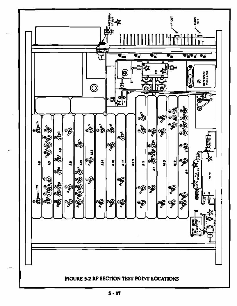
Refer to figure 5-2 for h t i o n of t a t points. Verify a u g d of U)MHz at approx. -9dB.M.
A normal signal indiata thrt the malfunction b rehted to a tanal able connedions or test equipment opcntion
Refer to f i 5-2 for bcation of test points. Va%y a aipd 1470M k at approx. -8 d0.M.
A normal aigd indiata but the rmlfunction m y krelated to the M2 .ucmbly. An abnor-ml aipd indiata a @Ian dated to the MI .uembly.

TABLE 6-8 FAULT ISOLAflON M1 ASSEMBLY
VLllCT m r r o u ~ r v r u r Emwe that properly opting test equipment
C W Y L C ~ U t eorrartly connected and applicable to the
1 test sequence.
APPLY INPUT
SlOUAL Apply r CW d p a l of 530 MHz r t r level of
1 1. \
-20 dBM.
UON1701 TEST POINT
=I
Refer to figure 5-2 for location of test points. Vaifj a -1 of 1470 MHz rt rpprox. .BdBM.
A normal signal indicates but the malfunction t related to a t d ab l e connections or test equipment operation
UONITOI Activate K5 by applying +28 VDC at 1122-17 TEST POINT
-6-and r signal of 1470 MHz at rpprox. -16.5 dBM.
Lobte the a u s e of the d u n d o n and repair o r rrptce.
.ONtTOn RIT Pm*T
Verify a d g d d 2000 MHz at approx. +7 - m - dBM.
bobte the a w e of the d m c t i o n and repair or rcpbce.
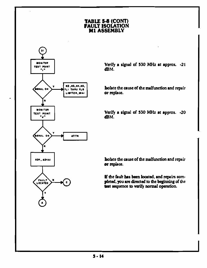
TABLE 5-8 (Corn)FAULT ISOLATION HlASSEMBLY
uoulmn Vcrify a signal of 550 MHz at approx. -21n w mur. . I dBM.
1 2 .KS.14.11. Isolate the ause of the dunctionand rcpair~ L ITMIU CLO LlWI1Cn.wI.l o r replace.
m O Y I 1 o n TCIT POINT Vcrify a signal of 550 MHz at approx. -20
=.I- dBM.
AW. A I 4 A I Isolate the ause of the dunction and rcpair or *cc.
lf the huhhskm bated, and repaincorn-pletd.youucdiread to the bqhningof the tat re~umoct o e n o d option.
-

TABLE 5-9 FAULT ISOIAlION M2 ASSEMBLY
Apply r CW signal of 1470 MHz at r level of 4dBM.
Refa to figure 5-2 for beation of t a t points. Vaify r signal of 30 MHz at rpprox. -9 dBM.
Vaify proper able atnnections and cable loss lrcton for interconnecring coax line within the RF section
Vaify r signal of 2000 MHz at rpprox. +10 d0M.
Refa to figure 5-2 for bation of test points. Vaify r S@d of 500 MHz 8t 8pproX. +12 dBM.
Vaify r signal of 125 MHz at rppmx. +5 dBM.
M t e the uwof rbc d f h c t i o n and repair or rcpbcc.

Isolate the museofthe malfunction and repair or replace.
Refer to figure 5-2 for h t i o n of test points. Verify r signal of 125 MHz at rpprox. +7dBM.

OlUS PAGE WlZhTIONALLY LEFTBLAMO
. APPLY
DI@NAL AT TI*? POINT "A"
4 ~ O Y I T O R
TL*? PDIU1"D"
@O*lTOR TL*T PO~YI-O-
AM,AlB ,A l~ ,A l7 , AI*[email protected],UI, DVNTU @LEIION
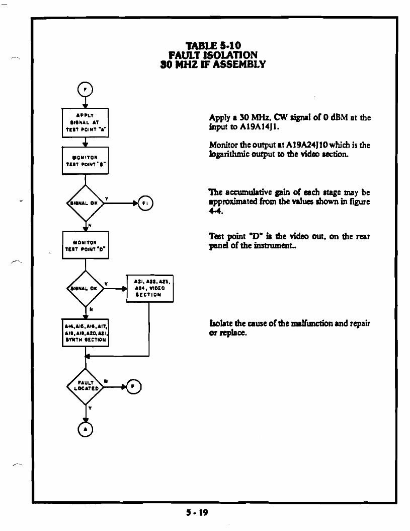
TABLE 5-10 FAULT lSOLAnON
30 MHz IF ASSEMBLY
Apply a 30 MHz.CW s i p 1 of 0 dBM at the input to A19A1411.
Monitor the output at Al9A24J10 which is the bgarithmic output to the vidso acction.
Ihe acmmStive p i n of mch stage my be approximated Crom the nlua&own in figure u.
Tat point P' is tbe video out. on the rear pand of the inswummt..
b t t e the cruse of the d d o n and repair or replace.

TABLE 5-10(CONT)FAULT1SOLATlON
SO MHZ IFASSEMBLY
A CPLY ~ I ~ Y A LAT Apply 8 30 MHz 8t 0 dBM 8t
TLIT ~ O I Y T . ~ " A 1 9 A 2 4 J 1 7 .
4 ? Tsl point %' i s the output of the IF nage.
UOYlTOll TEST m w .c" A19A29j12. V&fy 8 30 MHz Cig~ l .
V d y proper able mnnections mdable loss facton for intemmatbg oou l ins within tbe IF Icetion.
Lolate the awof the matfunctionmdrepairA24.U!4A26,u r , ~ ! e . ~ z s . or replace.
V I M 0 a€CTmN
-

--- ----
100 ID0 t w
( A l )
0 0 0 0 A*CI W K U t WOKMI tDOIM1 000KI ia O+IaV
wrrurv (A3 l -41-
,rma 0 l is t -2 ) #*m* ( A 2 5 1 ( A 2 0 1 eU:k? (A30-1) OOEMI QOKUI r w r w a MOIWZ (~10) I 0
0 0 0 0 o +lev o a r c r O 0 0 0 w r 4 8 0
(A231 lay*IYCUT 0 0::TL'g8WUIO
0 - l e v (A221 *,avo 41, IF DCT. (A21)A r c 1 0
---- ------. (AS) 0 0 0 ( A 2 4 1
OUlCUT
808W1 100M I 8 O W I ( A 9 1 I C 0-10 v zL ( IOWTrn
(*SO-5) WWUT 'I4 M I U I - I ~ V T O LO* Ir 0 O I U P U T 0 0 0
*--
(*so-2) " N 0 8 ~ ? l Q y f i v 8 .8 -m .46 InaI.0 OJ*+ l 8 V
800 MI 1 w M r #O M r (A81 IF IUFUT
0 0 0 IUCUT
aecr ( A 7 1 ( A 6 1
APPLY 8IBNAL AT
T E I T POINT *A.
I O Y I T O R T E I l POINT .E-
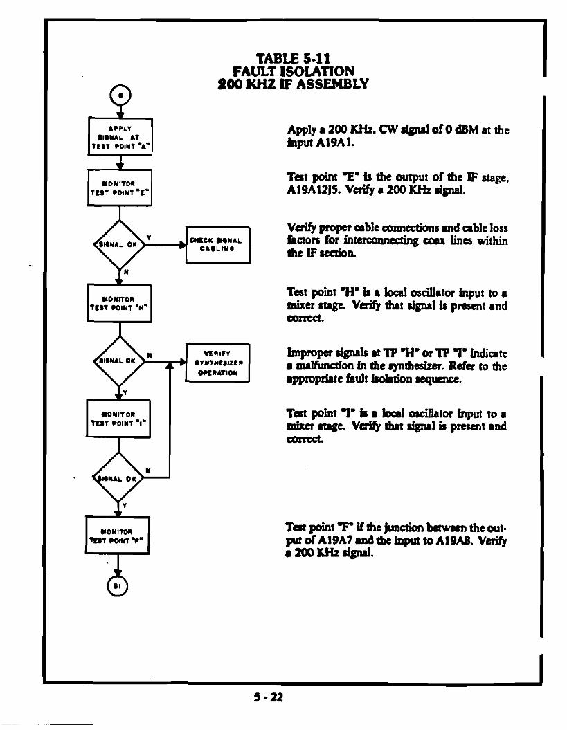
Apply r 200 KHz. CW dgnrl of 0 dBM rt the fnput A19A1.
Tcst point 2' the output of the IF stage. A19A1215. Vcxify r 200 KHz signal.
Verifjproper cable ooanationsand able loss OlLCU ..NIL
C A I L l Y l b a o a for intmxwnecting coax line within the IFwetion. I Tcst point 'H' t r local osdhtor input to r mixer stagc Verify that s i p 1 is pmcnt rnd 00rr#1. I Jmpropcr sipb at TP W' orTP 1' indimre
mlfunuion in the rynthairer. Refer to the 8pprc@te bult hobtion re~uarce.
I
mONITOR I E I T POlYl - I "
Test point 1't r b l adla tor input to r mfxa stage Verify bat d p l is present and earred.
TCFIpoint Fifthe functionbetwenthe out. pt dA19A7 .adrbc input to A19A8. Vcxify 8 2 0 0 K H t ~ . I

TABLE5-11(CONT)FAULTISOIATION
100 M Z IFASSEMBLY
Isolate the causeof the malfunction urd repair VIOCO 8 L C T I M I or replace.
Apply r 200 KHz -1 rt 0 dBM to the input ofA19A8.
Tat point 'G' b the log output to the video d o n Monitor A 19A13J6 for r 200 KHz Bigm1.
A8,AIO,AI I ,AIZ VlDLO ~ C T I O N
W t e the aureofthe nulfunction md repair or *u.

L
TABU 5-12 FAULT lSOIA'TJON
30 MHZ VIDEO
Apply r 30 MHz righal, CW or modulated. d d a r to the signal used d e n the malfunc-tion was noted
ff the input signal is frsqumcy modulated. rdcr m stadng point HI.
Refer to figure 5 4 for bation of monitor points.
b k t e the awe of dfunctioa md repair or -=FJk=
Refer to figure 54 for location of monitor points. If the ibpuf dgIYl is unplihl& modulated rdcr to the stadng point H2.
M a tothe A7 cud rcbcrmticfor the bcltion of the BFO output monitor point.
b k t e the aw ofmrlfunetScmand repair or @ace.

TAB= 5-12 (COW)FAULT ISOLATION
30 MHZ VIDEO
YOUITOR .IJ*
Refer to figure 5-4 for location of monitor points.
Lolate the malfunction md repair or replace.
VOUITW AmJ1
Refer to figurc 5 4 for bcation of monitor points.
• U,.II,UB.U* Lolate tbe d m d i o n md rrpoir or replace. -8
5-25
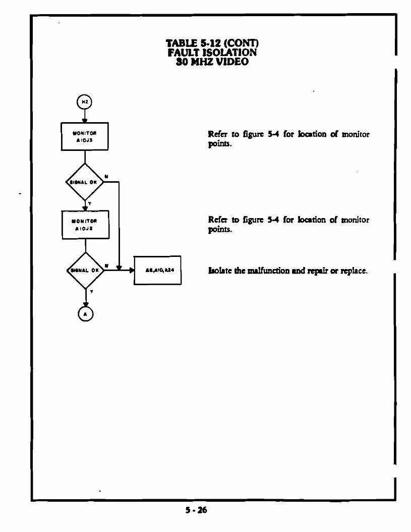
TABLE 5-12 (CONTIFAULT ISOLATION
80 MHZ VIDEO
YONITOI) Refer to figure 54 for h t i o n of monitor l l O J A points.
-
ION ITOR Rcfa to figure 5 4 for h t i o n of monitor 1 1 0 J 1 points.
lroktc the mrlfuadion md rrpiror replace.

TABLE 5-13 FAULT ISOLATION 200 KHzWDEO
V C l l t V T E S T
COUICYLUT
4 ACCLV I I C U T
. I@YAL
mOYITOn A 8 J 8
V A R V uco
O U T C U T
Apply a 200 KHz signal. CW or modulated. similar to the signal used when the malfunc-tion was n o t d
Kthc input s&nal is frequencymodulated refer to starting point 11.
Refa to figure 54 for bcltion of monitor paint.
lsokte the =use of d funa ion md repair or replace.
R d a to figure 54 for bcltion of monitor paints. U the input d g ~ li s amplitude modulated dertomrringpaint IZ.
Vary tbe oscilhtor output to obtain a beat fre- qucncy arder to the Khemrtic of the A7 card h r anoutput monitor point.
b h t c tbe mrlfundon md rrpritor replace.

TABLE 5-13 (CONT)FAULT ISOLATION 200 KHzVIDEO
>
10)1170R A ~ J B R d a to figure 54 for Location d monitor
points.
Lokte the malfunction and repair or replace.
U O Y l T W Refa to figure 54 for Location of monitor A B J 1 points.
-Lokte the malfunction md repair or replace.
,


('IliIS PAGE INTENTIONALLY E F T BLANK)


CMlS PAGE INTENTIONALLY lEm BLAMO
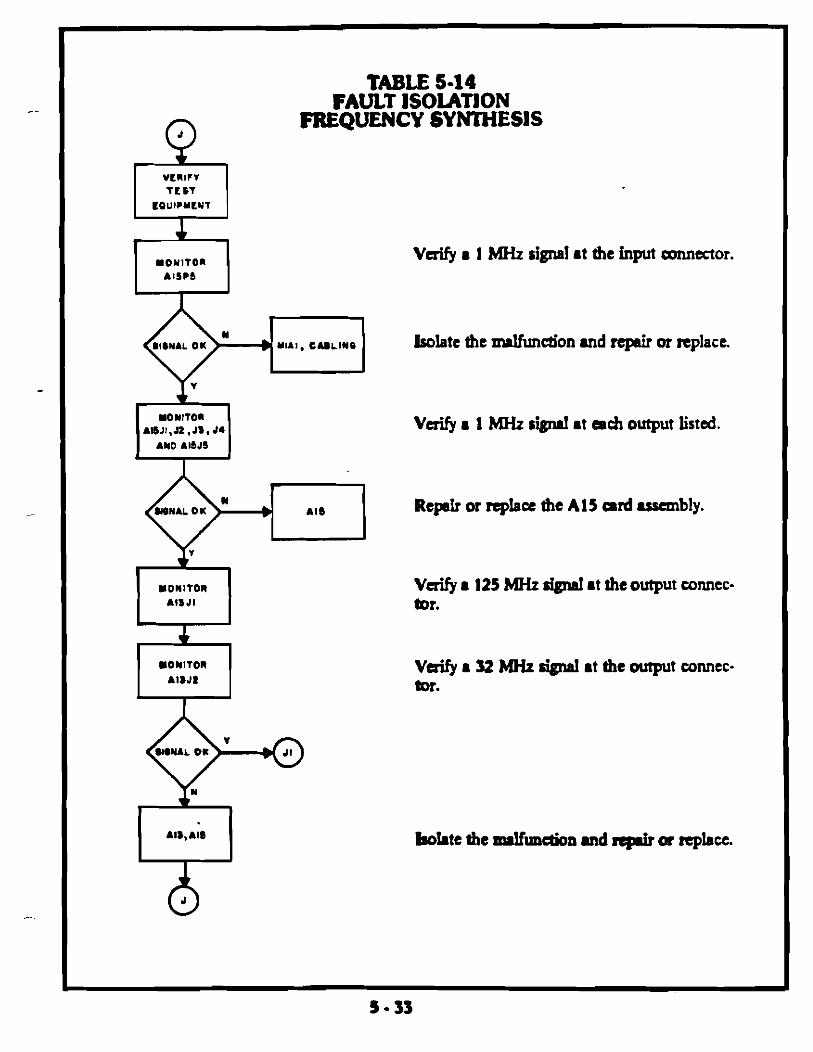
TABLE 5-14 FAULT ISOLATION
FREQUENCY SYNTHESIS 0
Verify r 1 MHz signal at the input canator.
blatc the malf~mdonand repair or replace.YUI. CULIUO
Verify r 1 MHz signal at a& output listed.
Repair or replace the A15 a r d assembly.
Verify r 125 MHz signal rt the output wnnec-tor.
Vaify r S2 MHz signal rt the autput wnnec-tor.
bokte the d1111ction and rrpItor teptce.
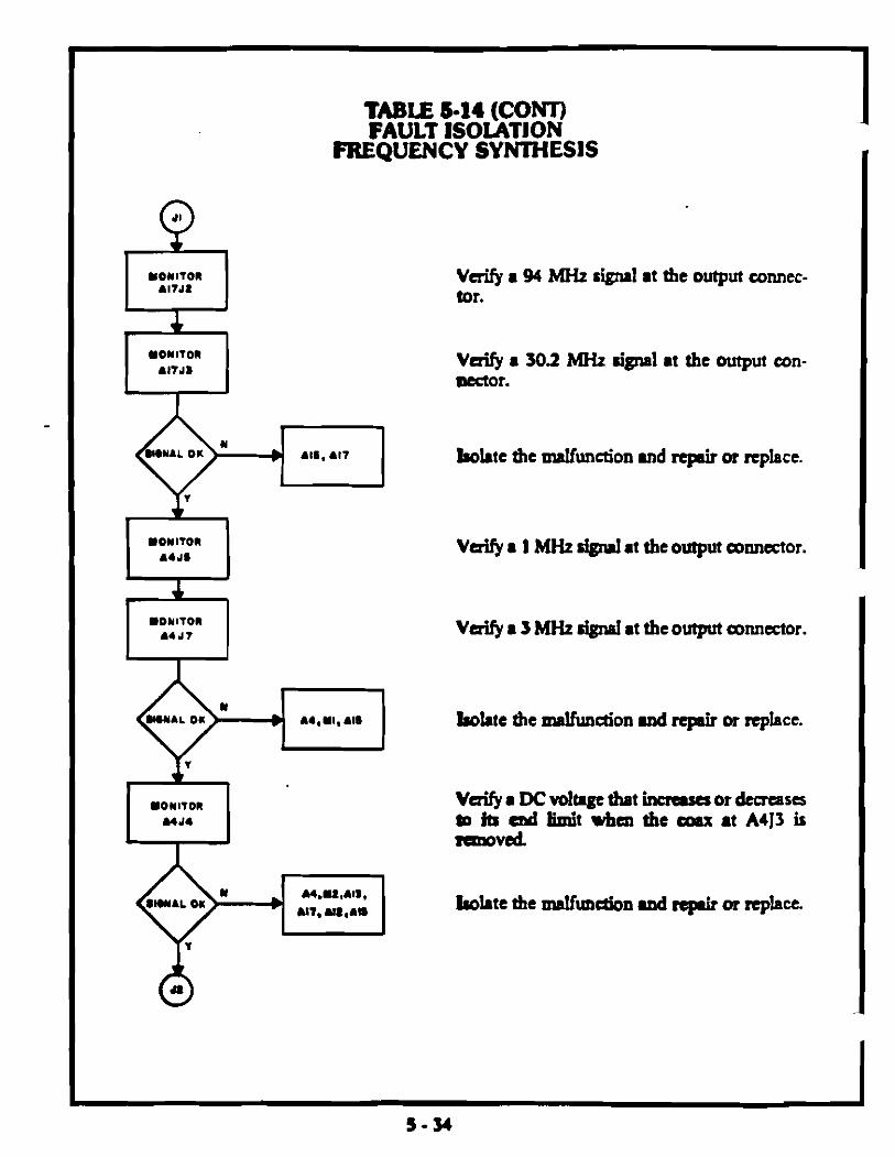
TABLE 6-14 ( C O WFAULT ISOlATlON
FREQUENCY SYNTHESIS
UO*ITOR .ITJI
V d y r 94 MHz signal at the output connec-tor.
4-~ 0 * 1 1 0 R
. l l J 1 Vaily r 30.2 MHz signal at the output con-nector.
418. .IT kokte the d u n a i o n md rrpirareplace.
.on ITOR .4JS
Vaily r 1MHz sigd at the output atnnector.
i .OYITOR
A 4 J 7 Vaily r 3 MHz rignrf at the output connector.
b k t e the rmlfunction mdrrpir or replace.
~ O * I T O R Vaily r DCvoltage that in- ordeaeasa WJ4 U ib ad limit vbm the cau at A413 is
raaoved
Lokte the d m u i o n and rrpitor replace.

TABLE 5-14 (COW)FAULT ISOlATlON
FREQUENCY SYN7HESlS
Verify an output frequency that Wies from 1 to 2 MH2 in 100 Hz steps as the tuning knob b rotated
Isolate !he rmlfunaion and repair or replace. A I 1 . D l K U . A l 5
Vcrify an output frequency that varies from 1 to 2 MHz in 1 Hz rtcps rr the huring knob is rotated
Al~.Dl*l lAL.AI5 bolrte b e mrlfunction and rrpair or replace.
Vwify m output fkqucncy that n r i e s from 52.8 to 42.6 MHz rr the tuning knob is rotated
Verify an output frrquency that n r i e s from 50.25 to 50.0 MHz at the tuning knob is rotated
. + Verify m output fkquency that vuies fromIONITOR
U I J 5 5 2 to 3.45 MHza the tuningb b &rotated.
-A I Z , ~ * ~ A L . A I S bolrte the mrlfunction and repair or replace.

(THIS PAGE INTENTIONALLY LEFT BLANK)

5.4 DISASSEMBLY
***CAUTION**+ thecam&pmwntdomogrbllmq&laod
~ - M & M & ~ - O T ~ purrcdbdghtadfnnnthemdngeonnsdrw. Lbe d r w m l ? & r ~ ~ d a l l p a s l b r ~ .b n o c bmdrl$dcoppu@da monlhon nocr-a y l o ~ N # d L h r m . ~ n s o r t h a u b W r .
Top and Bottom C o v m and SMB Connecton - 'Ibe d v a my be disassembled with ordi-my hand tools. Removing the top aver rllows rccas to the plug-in rssanblia in the a r d a g e .
NO^*** k b ~ r o p r w e n & m o g c r o C h e h c -rm L & t h S u B C o r a o d o r ~ r 4 p r ~ p a c $ kChemmdrdmoncroocaray id l&~~thc a n u u d o n o n C h e k p o o / t h d ~
The atmaor should alsobe used w h a t possible on similarconnaorsthroughout the receiver whether used with a d or flaible d a l able.
Inside the bottom amr arc individual covm that d o w recess to mbmanblia of the IF cb.szir. A19 &on.
hrmd
T o r c m o v e t b e r a r p n c l p d o m t b e f o ~ s t e p s .Mndlonrmmv&wedtomthe nu.
1. -paves=d
2. RQYmcopana.
3. Relate4 rtiLatcb6 .ad trmovc plug-inmodulr
4. R m v e 8KTCWS - 4 retaining ach of the control connectors located at the bottom leh c o m a of the panel. I b e hardware is sptive behind the pnel.
5. Remove 4 ruewr -rest the bottom edge of the panel.
6. Remove 2 rcrcrwr adjacent to the left ride handle.
7. R m v e 2 r u m s adjacent to the right ude handle.
8. Pull stmight mf on the panel until the connector louted next to the plug-in module connector t dbaumatcd h m the d m m e .
9. Rassembly my kaccomplished by perf- steps 1 through 8 in the muacorder.
.** CAVflON *** Urormdoaramthatthramncdwbmdng
pcpr l fyw&htkhc~conndor.¬ J k l D C I t i / r h e e o M c d o r r h o u r b r ~ ~ m c ~ ~ IImoybrnec~~rytoiruhadpmssunanduU. chmwldoh&a8gntkhcnwhmrdmton-hg thr rarrpacl.
il&akbd
Remove aU umvs from the pnel.
Right Slde Rae1
Perform the following rteps:
1. D i i p w r c o r d
2. Remove top ana.
3. Disconnect the 2 scmv on "mblmanatom bcrted on the bnckct at the r a r or the ude pncl. m d the 1-10connector toward the front panel.
4. Remove al ly lbe 8 rcmnbated rround lbe periphay dlbe side p n e l plu the 2 -b a t e d n-t the rru dgc of Qe pnd AUotherlaearruerecuriagcomponartstotbeddepnd
5. 7bac b suffidmt r d c c bop in the tcmrinIng abhtombw lbe r i d e p m l m l i e f L t k r i d e t h e ~ v a f o r ~ d r y l .Ifhbdecircdto a~mplctclydirconnecc lbe ride pncL Qe rrmrininp o~aaeaarrm yabcrteabyvirrnlinrpsctiw.

-6. To reinstall the pand, perform steps2 thro@ 5 in the m m e arda.
BQaeud
To temove the front panel perform the following rteps. DlrecUom m rn vkwed born the tonC
1. Disconnee! power cord
2. Remove top ma.
3. Disconnext the in-line connecton in the tigid arur bmted im-mrdistcly khind the POWER witch at the top, Mt a m m of the pnel.
.0.NO7E... L h 2 ~ m c h r o / t h c p f i ~ ~ l ~ t o O D d d d p m o B
4. Remove 4 rcrm narcst the bottom edge of the p n d .
5. Release the o t c h a and disamncct tbe 4 zcch@ar &aped eonnee-tors bu ted a m the front d t h e cud oge.
6. Using the SMB Connector Exmetor, disconnect the -tire bundle of maxi1 u b l a interconnecting the front pand with the top of the o r d ugc. This is the bundle comingup behind the AM SLIDEBACK aontml.
7. Remove 2 ramadjrcent to kft ride hmdle.
8. Remove 2 ramadjacent to right dde handle.
9. Remove the SMBown- to the kft ride of the front pncl b a r d
10. Slide the front pnclfonnrd until it it hd the reaim.
11. To rrinnan the froat pnel perform steps2 thmgh9in tbe meme a d a .
w

6.5 FXELD SERVICE ADJUSTMENTS
6.5.1 GENERAL
The following arc rdjummts h r may be requiredwhm 8 previously rdjuted -re assembly i,hulled in the receiva. No s p ' d tat fixture or quiprnents 8E requiredotha than those d+scn'bed.
Unless o t h d s e dirrdcd for @Cutr rdjushnents. the repbeanent wrd should be tem- pnrily h t a l l d using brt atendm ord to&. and ablcr nrpplied with the receiver.
The procedures mke w of 8 q u hdpd pocasd normally &mu& the receiver. 7 % ~50 KHz position of the BANDWIDTH 4- b tsod to route the d p l throuc the 30 MHz IF circuits md the 20 KHz position is rrrd for the theKHz IF. Unless othenvire s ~ ~ e d .the d v a is tuned to 10 MHz
*** CAUTION *** Twnq(/themdurwhcn manodno aCrtPlIing
I

.
5.5.2 A4 M I C R O W A V E OSCILLATOR PLL CONTROL
setup:
I iI +I__[ANALYZER
1 Iy-I SIGNAL I GENERATOR RECEIVER 03QIlATOR
Rocedure:
ARWeTSupplV
1. bt.1I Be A4 h a r d on the at=& cud
2. Monitor B e output voltage at 18.
3. Adjust Rl00 for +I5VDC*.1.
4. Monitor the voltage across aprdtar CS8.
5. Adjust R95 for -15VDCt.l.
8.Frrquefq Muhlplicr
1. Connect the signal -tor to 16.
2. k t t h e ~ ~ t o r f a rI MHt,cw.mtOdBM.
5. CoancarheordllorcopetoP.
4. AdjurtU.adU~~MHrGdputimtd2vol~.
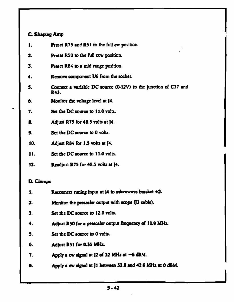
C Shpins Amp
1. b e t R75 and R51 to the f d m position.
2. Reset R50 to the full ccw position.
b e t R84 to 8 mid nnge position.
R ~ v m U6 from the loeket. a m p o l l ~ ~ t
5. Connect 8 h b l e DC source (G12V) to the junction d C57 and R43.
6. Monitor the voltage level 8t 14.
I 7. Set t h e D C m t o 11.0volts.
Adjust R75 for 48.5 volts 8t 14.
Set the DCm r c e to 0 volts. 1 9.I 10. Adjust R84 for 1.5 volts 8t 14.
11. Set the DC toraec to 11.0 volts.
12. Rmdjust R75 for 48.5 volts at v.
D. a-P 1. Rcanmect mbqjinput m 14 m rduwmvcbndtet +2.
2. Monitor the prrscllu output with ropc (15 able).
5. Set the DC m 12.0 volts. r o l ~ ~ ~
4. Adjust R50 fa lpramla wtprd k p n qd 10.9 MHr
5. SettheDCror~crmOvolts.
6. Ad@ R51 for 0.BMHz.
7. m l y 8 ~ d g d 8 t J 2 d U M H t U d d B M .
8. A # & 8 ~ d g ~ l i t J IbawernU.Bd42.6MHt.tOdBM.

1. Connca the p a l e r output to J3.
2. RcpLce component U6.
3. Monitor the prcsala output.
4. Vdfy that the 11 signal variesbawecn32.8 MHzmnd 42.6 MHz mnd thrt the presdcr output rimult.neouly varies ktwccn B MHzm d 10.6 M h
5. Radjust the upper damp to 11 MHt md mdjwt the lower drmp to the aulimrmrmluc t h t t a~atirtmtwith rtrbiiry mt .B MHz urd throughout Be q.
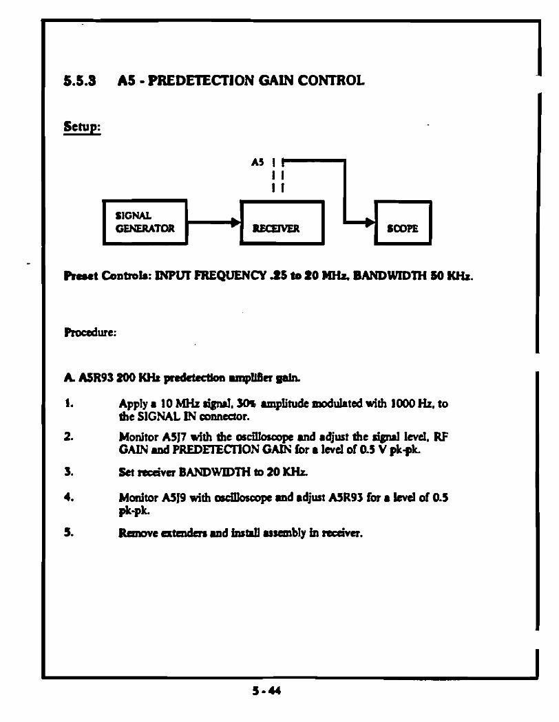
5.5.3 AS - PREDETECflON GAIN CONTROL
Setup:
RaetCootrob: INPUTFREQUENCY 3 5 to20 MHz. BANDWIDTH 50 KHz.
Pmxdute:
A ASR93 400KHz pndctcctknmmpWn #ah
1. Apply 8 10 hfk S @ d , U)s .rnplit~demoduktd 6th1000HZ,to h e SIGNALIN eonneclor.
2. Monitor A517 with h e orcillorcapc and adjust h e sipd level. RF GALN .adPREDEIEmON GAIN for r level of 0.5 V pk-pk
5. Set d v e r BANDWIDTHto20 KHz
4. M d t o r AS19 6thorIllorcapc and rdjrut ASR93 for r level of 0.5 pk-pk
5. Ranovc atadenand fnrhtl usanb!y in rrcdver.

--
6.5.4 A6-AGC RF OVERLOAD -AUTORANGING
setup:
SCOPE Ab
PlrutControk INPUl FREQUENN 0 to 2 5 MHz. AGGOFF. FR GAIN fully CW.
Rocedurt:
A A 6 R 1 4 - B M d l h 1 t Q d ~ d ~ l d .
1. Tune d v e r to 100 KHz
2. Apply r 100 KHz dgnal. SOs amplitude modulated with 1000 Hz. to the S I G W IN comsror. Adjust d g d gmmtor output level to -25 dBM.
3. Adjust A6R 14 to d c e the OVERLOAD Miator frtrt a&.
a.A6RB - Band 1Attmuator ardorurglngbv-kvcl(frrrdrold
1. R o c e c d u i n A l m d Z a e c p W ~ t o r o r r t p u t t o - U I d B M .
2. adheope to A6U5 pin 10.
3. Adjust A6R8 to nukc bre s i p ! aca~on the ordlbrcopepbbuc +s3 v dc 1on modulrtioa p k r .
4. Olefk mcnrntor ndomnging by fncrotiag the modulatioa kvd to 1m . n d ~ ~ t h c ~ ~ o r a p d l c v d l D + 2 o d B M .
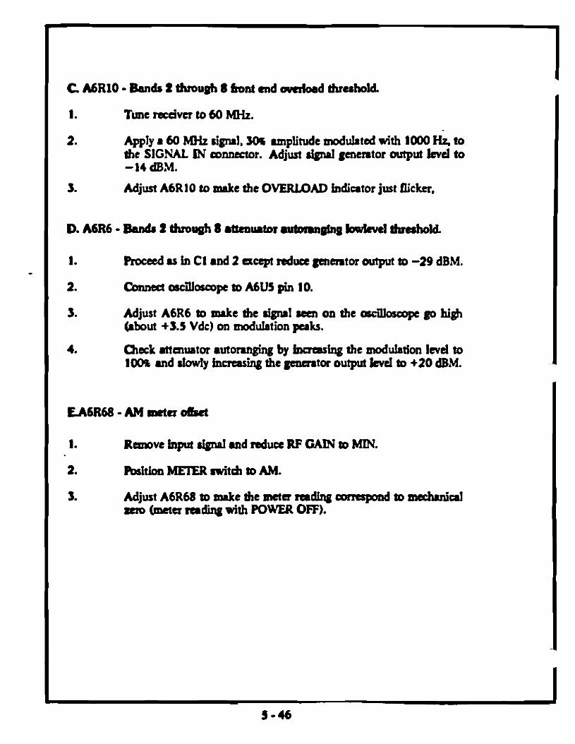
C A6R10 - Bands2throu* 8 h n i end GICllOlld threshold.
1. Tune d v n to 60 MHz.
2. Apply r 60 MHz signal, U)B amplitude modulated with 1000I&to the SIGNAL IN connector. Adjust dpd gcnentor output level to -I4 dBM.
S. Adjust A6RlO tomake the OVERLOAD indicator just flicker,
D.A6R6 - Bandr 2through8 aftmuator-@ng karlr\Ht Umxhold.
1. Proceed as in C1 8nd 2accpt reduce fenemtor artput to -29 dBM.
2. Cased adloscope toMU5 pin 10.
S. Adjust A6R6 to make the c i g ~ l on the d o s c o p e p high~ c n (.bout +S.S Vdc) on modulation p k s .
4. C%ak 8ltcnmtor 8utormging by hasring the modulation levd to lOOe and dowly increasing the gemator output level to +20dBM.
U6R68 -AM mrta o b d
1. Rmrove in@ dpdmd reduce RF GAIN to MIN.
2. Mtion MEIER rvitcb to AM.
3. Adjust A6R68 to make the ma mding axrespond to mffhujul om,beta mdingwith POWER OFF).

6.5.5 A7 - A-M m d BFO DETECTORS
SCOPE I S I G W GENERATOR
Fraet Com*ob: INPUT FREQUENCY 3 5 to tOMHr
Rocedure:
A A m 200 KHz m d 30MHz detector balance
1. Set BANDWIDTH10 50 KH5.(30MHz ddector)
2. A m 8 450 -1, -9S4B. 10Vel 10 the SIGNAL IN conn+dor.
4. hi t ion the BANDWMHrelector (D 10 (200KHr dotoe to t ) mnd again mtc tbelevelasinstcpf. ~ d r e l m ~ ~ ~ ~ ~ 3 l a d 4 u c r m s q u r l r d j ~ t A7R25 to equalize rhmwhile dtchhg betmcn the 20 .ad SO KHz W d t h p~siti~r~S.lo t . : . cbantea tbo 200KUc dotactor only
1 S e t t h e ai(mo1 (onorator t o a froqnoncy of SOlllc -95dBo 1 . ~ 0 1 .
J l o n l t o r UI VIDEO ont on .cop..

4. Let A H - l l - 8 1 0 muitch to 8 1 0 .
3. Adjunt A ? (available at top of A? ar#embly for sero beat on the #cope.
888NOE888
~ , R 2 5 , o d R 5 1 ~PI#rd~mcsA,BondC ~ h m ~ e b k ~ ~ b o t h t h c o ~ o o n d & k r e h w c e q ~ d / ~ d m o e ~ ~ k acMLu&Lrrpn#chmc.
C A7T51-rnKHrA-Mdrtcctordcdht
1. This adjustmcnr is not q u i d unless indioted by B.3. U necessary. q e a t proecdurcs A a d B. accp adjust A7R51 inttad of R6.
D.A J R ~ ~ - ~ O M H ~ B F O ~ U ~ ~ A ~ ~ ~ - ~ ~ ~ K H ~ B F O ~ 7
1. Set &va bandwidth to MKHz and paform poadure A. 1 3 m d 3 above. a#pttura OK ~ i g dmodulation.
2. Monitor A7PI pin R or 14 with the osdosmpe O b r m tbe audio beet I
aa on the oscillos#)pe and adjust A7RS2 for rmdmumoutput.
3. U m g e receiver bandwidth to 20 KHz and adjust A7R76 br muimum output kvel of the audio bat w e .
4. While altanrting ktwemhndwidth rmingrof20rod SO KHz, readjustother RS2 or R76 to m&c the higha orbput qur l to tbe lowaobtained in steps 2 and 3 above.
5. RcmovccdcadmladhttrI l~lyintscdva.
-

--
6.5.6 AS - 30MHZ LOG IF DETECfOR
setup:
*Ti,, Reset Cootmls: LNPmFREQUENCY .2S to 20 MHz. BANDWIDTH. 60KHz. AM VIDEO -LINEAR RF GAIN-w co9atu&kwLse.
Rocedure:
A A B R 6 9 - D C w
1. Monitor the ~ignalat the AM VIDEO connector with the oscilloscope. The dc level d the video rignal should k tclo. If not. ace the adjustment procedure for A10.
2. hi t ion the AM VIDEO witch to UX;.Adjust A8R69. Unsessay. to ren,the dchvddrbcdgnali&nonthedorcopc.
3. Remove amdmad inrtlll assembly in r d v a .
- -
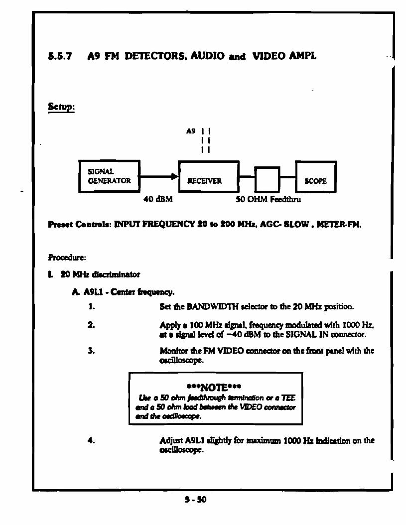
5.5.7 A9 FM DETECTORS, AUDIO and VIDEO AMP1 ~-
setup:
A9 l I 1 I I I
SIGNAL GENERATOR RECEIVER SCOPE
40 dBM 50 OHM Fkdrhnr
h u t Conbola: OVPUI FREQUENCY 20 to 200 MHz. AGC SLOW, HETER-FM.
Roadure:
I. tOMHrdi8ulmi~tor
A A9U-Crnsrr-.
1. Set h e BANDWIDlli rdector to h e 20 MHz position.
2. Apply r 100MHz -1. frcqumq modutted with 1000 Hz. n r dgd lev4 of -40 dBM to the SIGNAL IN connector.
5. Monhor the FM VIDEO -on h e h a t panel with the dv.
h
088NOm888 U u o 5 0 o h m ~ h ~ o n a o T E E
a n d o 5 0 d m h d b Q o m d r ~ O e o n n d a andtheodmape.
4. Adjust A9L1 di&tly for b r r m 1000 Hz fadimtion on the acillwcopc.
I

aA9R26-FUnwtrrokt
1. Uada the ame anditions u in A above. a c q t remove modStimfrom input aigarl, rdjust A9R26 for r center scale =ding on the TUNING meter.
C A9R30 - FUmrtrr galn.
1. While dtmting the dgnrl gcnmtor output frequency bc-tween 95 MHz and 105 MHz. adjust A9RfO for r meter read-ingof about 116 and 516 full sale rcs@vely.
0. mKHr DLnimtMtor
A A9U- h q v
1. Set the BANDWIDTH ulator to the 2 MHz position.
2. Continue aomplete procedure as inIA accpt adjust A9U.
B. A9R33 - FUllrtrrclbrL
1. Turn off ga~mtormodStioa rad adjust A9R33 for r center rcllc rsding om the 'NhWG maw.

While dtmvting the up1 gmmtor frequency be-tween 99.950 md 100.050 MHz. adjust A9R39 for r meter mding of about 1/6 and 5/6 f d d e .
111 100KHrDbuhhtor
A A 9 S Cmtrr kqueaq.
1. SU the BANDWIDTH relator to the 20 KHz position.
2. bntinuc amplcte u in I. A, accpt adjust A9L3.
Tum off gcnentor modukth d adjust A9R41 for a center rale mding on l e Thing mcta. I
C A9R46-FMu~ttrgabL
1. While dtemrtbg brc signal -tor output frequency be-tween 99.975 and 100.025 MHz,adjwt A9R46 for r meter mdhgofabout 1/6and 5.6fullralr

IV. 1 O K H Z ~ t o r
A A9LA - h t e ~Frequency
1. Sa the BANDWDTH selector to the 10 KHz position.
2. Continue wmplde pmccdw as in I& aacept adjust A9U.
B. A9R47- FM meter offcet
1. 'Ibm offgcnartor modulation d adjust A9R47 for a center =le mading of the Timing mda.
C A9R52 -FMmeter gain.
1. While dtrmrting the -1 gcnmtor output frequency be-tween 99.995 m d 100.005 MHz, adjust A9R52 for 8 meter readingof b u t 116 a d 516 full d e .
.+ONOTEOOO
Tho@ubn~~~ojprocrdurrrN.ABondCfn-~~mcr~:haUebbe~rrprolrd~thrdcprrrd d n g s am owned

.
5.5.8 A10 A-M VIDEO-SLIDEBACK PULSE-AUDIO STRETCH
SCNE
1"""k.l-1V I D E O O U T
h 8 e l ~ o t o ) :lNPVf FREQUENCY .S $0 10 HHz.BANDWIDTH SO M H Z AM VIDEO -UNlUR RF G m - mw-. PRU)RECnON GAIN-0.
hcdurc:
A AlORls Vibo dc alhL
1. Monitor h e signal at h e AM VIDEO ta~eaorwith the osdlos~ope.
2. Adjust AlOR 18. Unrmury, to ~ m ,the dc kvdof the dgnd s e n on the orallorcope.
( A 1 0 1 1 8 i o aroilabla from top o f A 1 0 onoembly; axtender not topoired)

I
5.5.9 A l l Los i c and Switching Cont ro l
a E T U C :
I
B I Q N A L R E C E I V E R B C O P E IQ E N E R A T O R AM V I D E O *
Procedure:
1. Monitor a i 8 n a l a t AH V I D E O connrc to r on ecopr .
I. S e t t b e a i s n a l Ranera tor -9SdBmt o 1 0 0 1 1 ~ ~ l e v e l .
3. Tone r e c e i v e r t o 100H8x. I00KHr BW, a t t e n u a t o r 0, p rede t ac t 8 . i ~ 0.
4. A d j u r t m23 ( a v a i l a b l e from t o p of A 1 1 ar rembly) f o r 1 v o l t o u t on .cope.
B. A1152S MDC OAin Conpenration
ROTE 8 T b i r i r a DSI Sya ten a d j o a t n e n t and a n o t r e q u i r e d f o r a tanda lone ope ra t ion .
1 Lnrore t h a t and-to-end s a i n i a c o r r e c t aa i n t b e procadurr .
S t e p A. Monitor a i e n a l a t AH VIDEO connec tor on acope.
- I. Connect conpo te r t o r e c e i v e r I E E E po r t .
3. Pu t r e c e i v e r i n q n a r i remote mode (command 114).
4. S e t e i ~ n a l Remerator t o 10018x, -82dBn l e v a l .
5 Tone r e c e i v e r to 1 0 0 1 8 ~ ~ t o 0,o a t a? a t t e n o a t o r # e l e c t I00KHs bandwidth.
6. A d j o r t All525 ( e v a i l a b l a from t o p of A 1 1 aaaanbly) f o r 1 v o l t peek v idao o i ~ n a l .
5.6 HARNESSESAND ~ C O N N E C T l O N
&me 5 6 rbovr tbe cud age am atrmatw baths. Table 5-15 Em cbeam hmess oormeaion,totbecudr..adrbaanwbaetbenriaurmmlovted.
TbMe 5-16 5-26are i t t ~ thewirirU(not apu)bcrvecn the roccivcn modules doaneetorr. .
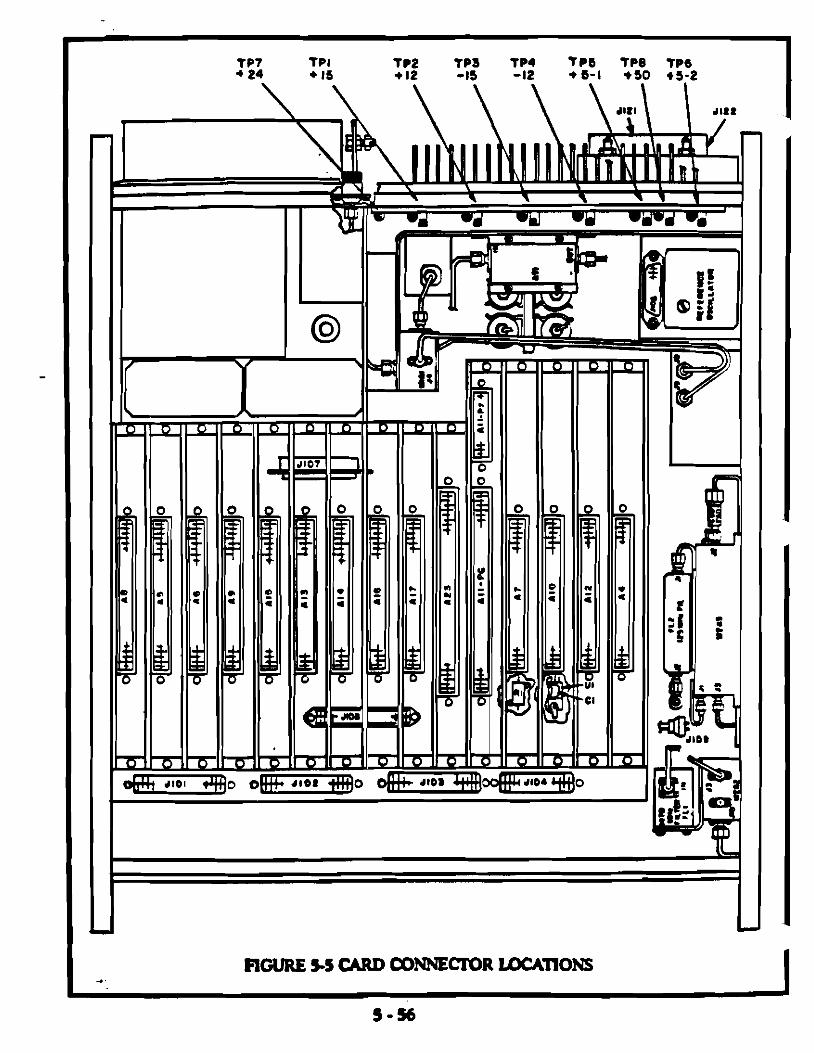
TP7 TPI TP2 TPS TP4 T P I TP8 TP6 24 -12 I +50 t 5 - 2
FIGURE 5-5 CARDCONNEmR LOCAIIONS I

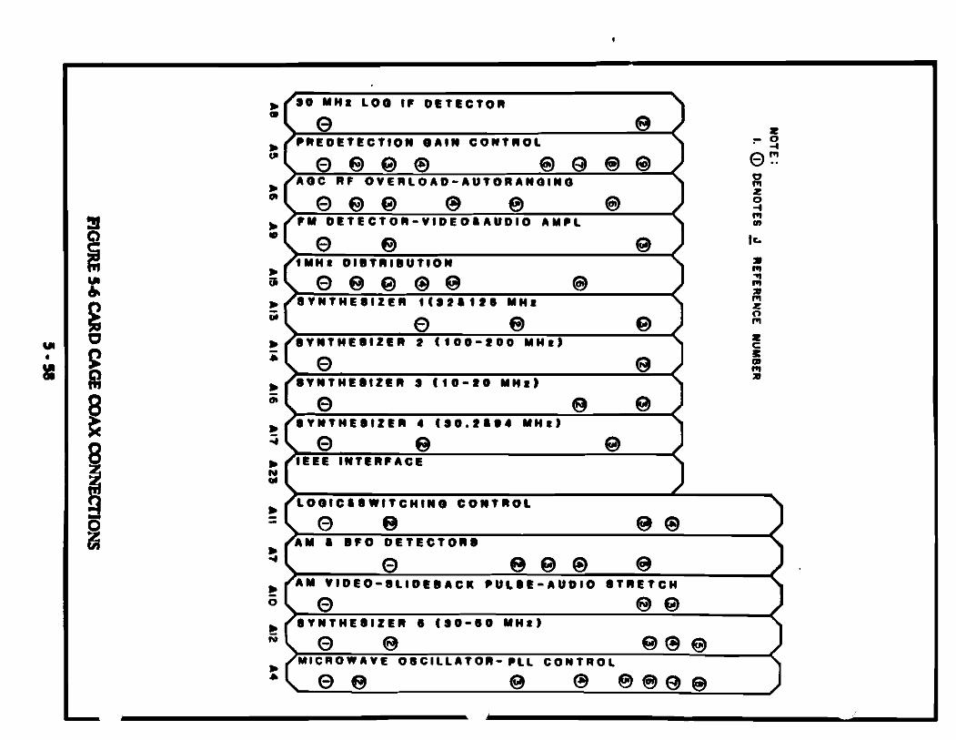
C n E o t t t c t t o n o A l n C O W T ~ O L 6
I ) - V I D E O a A U D I O A Y C L @
8
3 80 l V I ( T M E l I 2 E I I 2 ( 1 0 0 - S O 0 Y M c )-
* Q ,- l Y W T M E l l Z C I I a ( 1 0 - S O Y M c ) a 0 6
I J V M T M E ~ I Z ~ ~4 t s o . r r e 4 Y M S )t J 0 8 , I E L E I n T E n F A C E
0 N a
, L O O I C ~ ~ W I T C M I ~ Oc o n t n o t -- 0 Q A M a B F O D E T E C T 0 l ) b: 0 8 0 0 A M V I D E O - 8 L I O t B A C K C U L l t - A U D I O l T n E T C ME
0 0 k l V M T M E l l Z t I I 6 ( a 0 - 6 0 Y M C ) N 0 8
M I C R O W A V E 0 8 C I L L A T O l l - P L L C O N T R O L, 0 8 8 @ @@0@

CMlS PAGE lNI'ENI1ONALLY LEFT B W )

CARDCAGECOAXIAL CONNECTOR LIST TABLE 5-15 -
Assembly Connector S i l Connects To
A4 32.8 to 42.6 MHz A1213 32 MHz .8 to 10.6 MHz
A l y 2uWave Bkt r 2
VCO Tune uWave Bkt r 2 15 6
lMHz out I MHz Input3MHz +15V
A1 lJ4 uWave Bkt r1 Al9J2 uWave Bkt r 2
200KHzIF A1915 30 MHz IF A19112
A24J7 IF in A24 3 0 ~Pred IF ~ ~ A91I 30 MHz Pred IF A71 1
8 200KHzRedIF A912 9 200KHzRedIF A713
AGC Sig 30 MHz IF Overload
A1013 A1919
200 KHz IF overload A1913
3%' A1 113 A19
AGC 2 A19 30MHzPdIF M17 30 MHz Lag Video 200KHzRedIF
A812 A5J9
200 KHz log IF Ave Det Output30 MHz IF
A19J6 A101 1 A19110
1 30 MHz LogVidso 30 MHz Pred IF
A712 A96
2 200 KHz Red IF A518 FM Video Ou"rt Ave Detected ideo Input Video Output AGC SignallMHz
A2415 A7J5 A2413 A61 1 A24Al J3
RFGain.hh RF Gaii
A24 A6J4
lMHz A4J5 1MHt A1511 1-2 MHz Al6J2 32.8-42.6 MHr A4J1 U).25-50.01MH~3.2 -3 A5 MHz
A1917 A19J4

CARDCAGECOAMLUST(COW
Assembly Connaxor Signal
A13 125MHz 32 MHz 1 MHz
A14 1 MHz 1-2 MHz
A15 1MHz 1 MHz 1 MHz 1 MHz 1 MHz 1MHz lMHz 1-2 MHz 1-2 MHz lMH2 94 MH2 30.2 MH2
Connects To
uWave Bkt +2 A412 A1515 A15J4 A 1 613 A12Jl Al7J1 Al6Jl A1411 A1313 uWave Bk + 1 A1513 A12J2 A14J2 A15J2 uWave Bk +2 A1911 1

R-125B WIRE L I S T
SIGNAL NAME
+ isv + i S V + i S V +15v + 1 5 V +1SV +15v +1SV +15v + I S V + l S V +15v +1SV +15v -1%' -15v -1%' -1%' -1% -15V -1% -1SV -1SV -1SV -1SV -1SV -1%' +12v +12v +12v +12v +12v +12v SYNTH. 5 V REG. I N +12v -12v -12v -12v -12v -12v -12v CINALDG+5V 6NALDG+SV ANALDG+SV 6NALDG+SV 6NALDG+SV CINCILOG+SV M L O G + S V 4taLOO+W
WIRE COLOR
RED RED RED RED RED RED RED RED RED RED RED RED RED RED V I0 V I O V I0 V I O V I O V I O V I O V I O V I O V I O V I O V I D V I D RED RED RED RED RED RED ERN RED RED V I O V I O V I O V I O V I O V I O 6RN 6RN 6RN GRN 6RN 6RN BRN BW
WIRE FROM FROM TO TO BAUGE CONN PIN CONN PIN
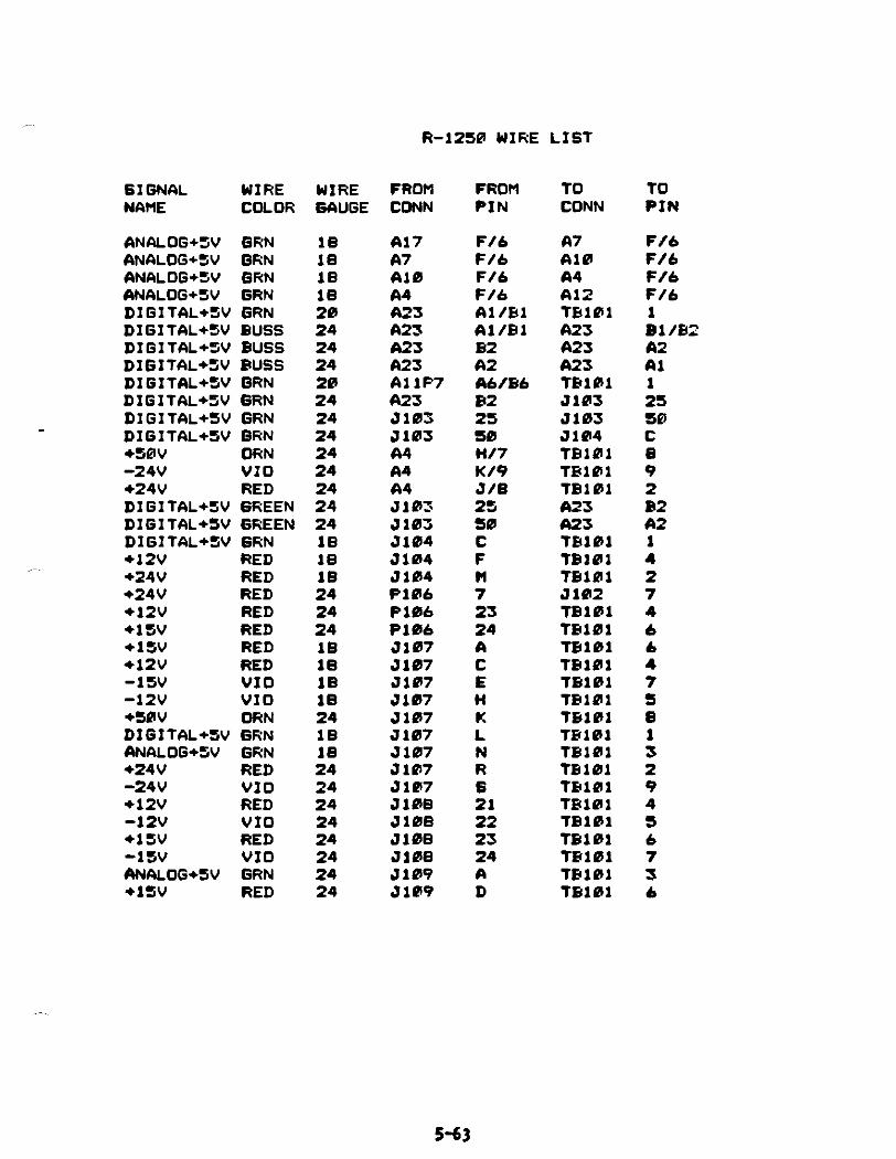
R-125m WIRE LIST
6IGNAL WIRE WIRE FROM FROM TO NAME COLOR G4UGE CONN PIN CONN
AN4LOG+SV ERN ANALOG+SV QRN ANALOG+SV GHN ANALOG+SV GRN DlGlTAL+SV SRN DlGlTAL+SV BUSS DIGlTAL+SV BUSS DIGITAL+SV PUSS DlGITAL+SV QRN DIGlTAL+SV GRN DIGlTAL+SV GRN DlGlTAL+SV QHN +5BV OHN -24V VIO +24V RED DlGlTAL+SV 6REEN DlGlTAL+SV GREEN DIGITAL+SV 6RN +12V RED +24V RED +24V RED +12V RED +15V RED +15V RED +12V RED -15v VIO -12v VIO +56V ORN DIGITAL+SV GRN ANALOG+SV GRN +24V RED -24V VI0 +12V RED -12v VIO +15V RED -15v VIO ANALOG+SV GRN +lSV RED
TO PIN
F/6 F/6 F/6 F/6 1 B1/B2 LLZ A1 1 25 50 C B 9 2 B2 A2 1 4 2 7 4 6 6 4 7 s 8 1 3 2 9 4 5 6 7 3 6
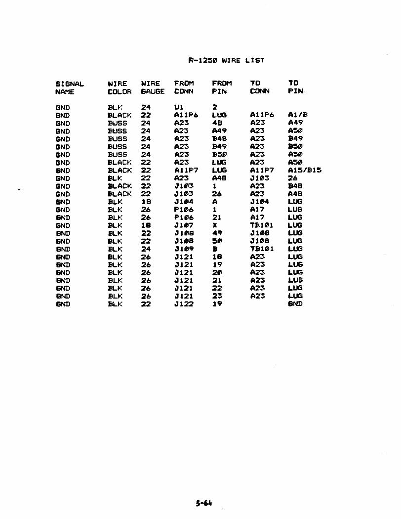
R-1256 WIRE L I S T
SIGNAL NCIME
GND GND GtJD GND GND GND GND GND END GND GND GND END GtJD GND GND GND GND QND GND BND BND BND GND GtJD GND
WIRE WIRE FROM FROM TO COLOR 6AUGE CONN PIN CONN
ELK 24 2 BLCICK 22 LUG BUSS 2 4 48 BUSS 24 (149 BUSS 24 848 BUSS 24 849 BUSS 24 850 BLACK 22 LUG BLCICK 22 LUG BLK 22 (14B BLCICK 22 1 BLClCC: 22 26 BLK 1 B (1 PLK 26 1 BLC: 26 21 ELK 10 X BLK 22 49 ELK 22 56 BLK 24 B ELK 26 10 BLK 26 19 ELK 26 26 BLK 26 21 ELK 26 22 BLK 26 23 ELK 22 19
TO PIN
A 1 /B A 4 9 A5PI 849 BS@ ASPI (150 (115/81CJ 26 848 (148 LUG LUG LUG LUG LUG LUG LUG LUG LUG LUG LUG LUG LUG 6ND

R-125@ WIRE L I S T
SIGNAL NAME
WBACL WPACL WBACL LSTAT ANALDG+SV ANALDG+SV +56V +24V -24V
WIRE COLOR
W/V WHT W/R WHT GRN BHN ORN RED V I0
WIRE FRON GAUGE CONN
FRDN PIN
C / 3 C / 3 C / 3 f / S F/6 F/L H / 7 J I B K / 9
TO T0 CDNN PIN.
Jlb2 P I 0 6 J122 A 1 l P 6 A l b A12 T B l b l T B l b l T b l b l

R-125b WIRE L I S T
61ONAL WIRE WIRE FRDN FRDN TO TO NAME COLOR GWGE CDNN P I N CDNN P I N .
RED RED V I D VJO RED VJD GRN W/V WHT W/V W/V W/V W/V
R-12SB WIRE L I S T
SIGNAL NAME
1BBdBLED* BIEdBLED* 60dBLED* 4bdBLED. ZbdBLED* BdBLED* 2bdB 26DP 48dB 4bdH AGCS* RFDL HAB MAC R*/L R*/L R+/L ATSWW* ATSW 1 b* ATSWBB* ATSWbP* ATSW48* -1sv -1SV +15v +1SV 9bdBLED. 76dBLED* SBdBLED* 3BdBLED l0dPLED l b d B -1BdB 3bdB 3bdP AH MET AGCF* DETDL )(CIA w
bLIVTo* BCLVTO* SAVTO* ATSW1bb* ATSW2@* ATW9br AT81J70. ATWSB* LWALOG+SV
WIRE WIRE FRDM FROM TO TO COLDR GAUGE CONN P I N CDNN P I N
YELLOW 2 6 J lb l YELLDW 26 J l a l YELLOW 26 J I B 1 YELLOW 2 6 J lb l YELLOW 26 J lb l YELLOW 26 J l b l WHT 2 6 P l b 6 WHT 26 J l 8 6 WHT 26 P l P 6 WHT 26 JllFB WHT 26 A1 l P 6 WHT 26 A1 1P6 WHT 2 6 A1 l P 6 WHT 2 6 A1 l P 6 WHT 26 A1 l P 6 WHT 26 A23 WHT 26 J llFS W/V 26 J1b2 W/V 26 J102 W/V 26 5102 W/V 26 5162 W/V 26 Jl02 VIO 2 4 as VIO 2 4 A9 RED 2 4 A5 RED 2 4 A9 YELLOW 26 J l0 l YELLOW 26 J lb l YELLOW 26 J l0 l YELLOW 26 J lb l YELLOW 26 J l0 l WHT 26 P l b 6 WHT 26 J l B B M T 26 P l 0 6 WHT 26 J l B B W /V 26 51914 WHT 2 6 A1 l P 6 WHT 26 A1 l P 6 WHT 26 A1 I P 6 UHT 26 A1 l P 6

R-I=@ WIRE L I S T
SIGNAL WINE WIRE FRDU FRDU TD T D NAME CDLDN GAUGE CDNN P I N CDNN P I N
ANCILDG+SV GRN 1B A 6 Y A9 Fl6
6IGNAL NAUE
LOG* +15v +15v -15V -15v +12v +12V -12v -12v ANALOG+5V ANALOG+SV fPlMHZI F
BFO TUNE BFO AUDIO
R-1256 WIRE L I S T
WIRE WIRE FROU FROM TO TO COLOR GAUGE CONN P I N CONN P I N
WHT A 1 lP6 RED A 1 lP7 RED A 1 0 V I O A 1 7 V I O A lP l RED A 1 7 RED A lP l V I O A 1 7 V I O A 1 6 GRN A 1 7 GRN A lP l WHT A 1 lP6
COAX COAX

R - 1 2 5 6 WIRE L I S T
61GNAL WIRE WIRE FROM FROM TO TO NAME COLOR GAUGE CONN P I N CONN PIN'
+15V RED 2 4 AB 8/2 A 1 2 B +15V RED 24 AB P/2 A 5 B/2 - 1 5 V V I O 2 4 AB C/3 A 5 C / 5
R-125B WIRE
SIGNAL NAME
FM MET +15V +15V -1%' -1%' +12v +12v -12v -12v ANCILOG+CJV aNF\LOG+5V FM AUDIO FMlnt:: FMlPlPlK FM2BBK FM26M
WIRE COLOR
W/V RED RED V I O V I O RED RED V I O V I O GRN GRN coax W/Vw/v W/V W/V
WIRE QAUGE
26 24 24 24 24 24 24 24 24 18 18
FROM FROM TO TO CONN P I N CONN PIN
R-1256 WIRE L I S T
SIGNAL NAME
WIRE COLDR
WIRE GAUGE
+12V RED PULSESTRCH W/V SLIDEBACK W/V SIDEBCKVDL W/V SLBACk: WHT
VBWD VBWD
W/V W/V. . . - -
+1SV RED +15V RED -1SV V I O -15V V I O +12V RED -12V V I D ANALDG+5V BRN ANALOG+% GkN PULSESTRCH CDAX AH AUDIO CDAX VPWC w/v VBWB W/V VBNA/NF4M W/V
FRDM CDNN
A 1 0 A l b A 1 0 A 1 6 A l b
A 1 0 A l b
A 1 0 A l d A 1 0 A 1 0 A 1 0 A 1 0 A l l 3 A l b A 1 0 A l l 3 A 1 0 A 1 0 A 1 0
FRDM T O T O P I N CDNN PIN

Rv12SC WIRE L I S T
6IGNAL WIRE WIRE FROM FROM TO TO NAME COLOR EAUGE CONN P I N CONN P I N -
+ l S v +ISV -1S'd
RED RED V I O
2 4 24 24
a12 a12 a12
P P C / 3
a8 a i r i l a10
8/2 B/Z C / 3
-15V V I O 2 4 A12 C / 3 6 l l P 7 P4 /&4 BD l * WHT 26 4412 D / 4 411P6 A l B
WHT ORN WHT WHT WHT WHT WHT WHT WHT WHT UHT GRN

R-125B MIRE L I S T
8IGNAL WIRE WIRE FROM FRDM TD TD NQME CDLDR GAUGE CONN P I N CDNN P I N
RED RED V1D V I O
CSB WHT CSB WHT
GUN GUN WHT
WHT
R - 1 ~ 3 0 WIRE L I S T
61GNAL NAME
ODBF0D ODBFBC ODPFPlB ODBFPlA ODBF1D ODBFl C ODPF1B ODBFlA ODBF2D ODBF2C ODBF2B ODBF2A ODBFSD ODBFSC ODBFSP ODBFSA +1SV +1SV -1SV -1SV ANALDG+5V C\NaLOG+5V SYNS
UlRE COLOR
UHT UHT UHT WHT WHT UHT UHT UHT UHT UHT UHT UHT UHT UHT UHT UHT RED RED VIO VIO GHN GRN UHT
UlRE FROn FROM TO TO GAUGE CONN PIN CONN PIN
R-1250 WIRE LIST
SIGNAL WIRE WIRE FROM FROM T0 TO NAME COLOR GAUGE CONN PIN CONN PIN
RED RED RED VXO VIO VI0 RED RED RED VIO VIO VIO GRN 6RN GRN

R-12SB WIRE L I S T
WIRE COLOR
UHT UHT UHT UHT UHT UHT UHT UHT RED RED v 1 0 v 1 0 GRN GRN UHT UHT
WIRE FROM FROM TO TO GAUGE CDNN PIN CDNN P I N
61GNAL NAME
+15v +15v -15V -1%' +12v +12v -12v -12v &NALOG+SV ANALDG+SV DUN. CONV. DUN. CONV. 94HHZPUH
94MHZPUH 6ND GND
WIRE COLOR
RED RED v10 V I O RED RED V I D V I D GRN WsN WHT WHT WHT
WHT BLK PLK
WIRE FROM FROM TO BAUGE CONN P I N CONN
A17 J / B 417 LUG 417 LUG
TO P I N
812 87/47c/s C / 3 D / 4 D /4 E / 5 E / 5 E / 5 F/6 439 26 H/7

R-125P WIRE L I S T
SIGNAL WME
DIGITAL+SV DIGITAL+SV DIGITAL+SV DIGITAL+SV ADDHB ADDR 1 ADDH2 ADDR3 € 0 1 ATN 6R0 NHFF' NDAC DAV REN 1FC GND
GND BND GND 6ND DIGITAL+SV
POR*
PDR* . . ACCEPTED*
DTAVL* DTAVL* COMF'CLR* CDMCLR*
R* /L DaTAPI* DaTA l * DaTA2. DATAS*
.+5V
WIRE WIRE FROM FROM TO CDLDH GAUGE CONN P I N CONN
BUSS A23 GRN T B l b l BUSS =3 GREEN 5163 WHT A l l P 6 WHT A1 l P 6 WHT A l l P 6 UHT A l l P 6 WHT 5121 WHT 5121 WHT 5121 WHT 5121 WHT 5121 WHT 5121 WHT J l Z l WHT J l Z l BLK J16S
BUSS BUSS BUSS BLACK BUSS
WHT
WHT WHT
WHT WHT WHT WHT
UHT WHT WHT UKT WHT
BREEN YClT YClT YClT YHT YHT YHT YWT YHT YWT
TO P I N
A 2 1 82 58 A 6 Bb A 7 87 5 11 16 7 B 6 17 9 26
48 A49 856 LUG A1/El
R-12Sb WIRE L I S T
SIGNAL NAME
D I b 6 D I b 7 D I b B 6ND END END END QND 6ND QND
- END QND LOGICGND
WIRE COLOR
WHT WHT WHT BLACK PUSS PUSS BLE PLK PLK BLK PLK BLC: PLK
WIRE FROM GAUGE CONN
FROM P I N
P 4 5 ,846 B47 848 849 B5B LUG LUG LUG LUG LUG LUG LUG
TO TO CONN P I N
14 1s 16 1 B4B P 4 9 1B 19 2p1 21 22 23 24
R-12% WIRE LIST
SIGNAL MINE NAME COLOR
DIGITAL+SV GRN DIGITAL+SV QRN DIGITAL+SV GNN DIGITAL+5V GRN +24V RED
ANALOG+SV BRN ANALOG+5V GRN ANALOG+SV BRN
+lZV RED
+lSV RED
+SbV ORN +SbV ORN
BND PLK QND BLC:
+24V RED +24V RED
+12V RED
+12V RED +12V RED +12V RED -12v VI0 -12 VI0 -12v VIO -12V VIO +15V RED +1SV RED +13V RED +l5V RED
-13V VI0 -1SV VI0 -1 SV VI0
-24V VIO -24V VIO
WIRE FROM FROM TO TD GAUGE CONN PIN CONN PIN
1 1 1 1 2 2 2 3 3 3 4 4 4 4 4 5 5 5 S 6 6 6 6 6 7 7 7 9 e 9 9
LUG LUG
R-IZSIF WIRE L I S T
SIGNAL NAME
BWSePILED* BW2PIBLED* DETOLED* BWlbGILED* PDOLED* BW'JPILED* PD1 @LED* BWZbLED* PDZPILED* BW 1RILED* PD3PILEDI- BUSLED* 3bMHZLED* BWZLED* 2bbMHZLED* BWlLED* KHZLED* KHZLED*
1DbdBLED* 9bdBLEDe BbdBLED* 70dBLfD1 bbdBLED* SadBLED* 4bdBLEDe 391dBLED ZBdBLED* lbdBLED RFOLED*
WIRE WIRE FROM FROM TO TO COLOR OAUGE CONN PIN CONN PJN
YELLOW 26 J l b l YELLOW 26 J l b l YELLOW 26 J lb l YELLOW 26 J lb l YELLOW 26 J lb l YELLOW 26 J ld l YELLOW 26 J ld l YELLOW 26 J l b l YELLOW 26 J lb l YELLOW 26 J lb l YELLOW 26 J ld l YELLOW 26 J lb l YELLOW 26 J lb l YELLOW 26 Jlbl YELLOW 26 J lb l YELLOW 26 J lb l YELLOW 26 J l b l YELLOW 26 J l b l
J lb l J l0l J l b l Jib1 J l b l Jib1 J ib1 J ib1
YELLOW 26 J10l J l b l
YELLOW 26 Jl0l YELLOW 26 J l B l YELLOW 26 Jl0l YEUOW 26 Jlbl YELLOW 26 J l B l YELLOW 26 J lb l YEUOW 26 J l b l YELLOW 26 J10l YELLOW 26 J I B 1 YELLOW 26 JlQ'l YELLOW 26 J lb l
J l b l YELLOW 26 J l b l YELLOW 26 J l b l YELLOW 26 J10l
J l b l Jlbl J l b l J l C l J10l J I B 1

R-1256 WIRE L I S T
SIGNAL NAME
BWSWCl BWSW1 BWSW2 DWSWf BWSW4 +24 +24 +24
SL IN*
RBB EBB CALRLY BDlEN DBS/BEN* BDS/BEN* BD1/2EN*
PDSWA PDSWB
laACL W A C L PREBl
WIRE CDLOR
W/V W/V W/V W/V W/V W/V WHT RED
W/V W/V YHT
WHT
W T
YHf
WIRE FROM FRDM TO To GAUGE CONN P I N CONN P I N .
26 A t 1P6 26 A 1 l P 6 26 A1 l P 6 26 A1lF6 26 A1 IF'&
J l b B 26 J l b B 2 4 PI66
26 26 26
26
26
?b

R-1256 WIRE L I S T
6IGNAL WIRE WIRE FROM FRDM TO r o NAME COL OH SAUGE .CONN P I N CDNN PIN
PULSESTRCH W/V SLIDEPbCK W/V 6IDEBCC:VDL W/V

R-l=B WIRE LIST
FROH FRDH TO CONN PIN CONN
SIGNAL WIRE NAHE CDLDR
GND BLACK
DTAVL* WHT DTAVL* WHT R* /L WHT DATAE WHT DATA 1 WHT DATA2 WHT DATA3 UHT ACCEPTED* WHT POR* WHT
CONPCLR* WHT COHCLR* UHT ODBFBA WHT ODBFBB WHT ODBFBC WHT ODBFPID WHT ODBF1A WHT ODBF1B WHT ODBF1C WHT ODBF 1D WHT ODBF2A UHT ODBF2B UHT DDBF2C WHT ODkF2D WHT ODBFSA WHT ODBFZB WHT
BND BLACK ODBF3C UHT ODBF3D WHT N26 WHT
WHT N22 WHT N23 W T N24 WHT N25 WHT =6 WHT w7 WHT NSB UHT Nsl WHT N32 WHT u34 W Nss mr N36 UHT Ns7 W
R-1 =6 WIRE
FROM FROM TO TO CONN P I N CDNN PIN^
6 1 GNAL WIRE NAME CDLDR
BDl* WHT BDZ WHT CSA WHT
CSB UHT '
WSLF* WHT DIGlTAL+SV GRN D l G lTAL+S V BRN
- DlGlTAL+5V GREEN
WIRE BAUGE
26 26 26
26
26 2 4 2 4 2 4
R-12513 WIRE L I S T
6IGNAL NAnE
WIRE COLOR
WIRE 6AUGE
FROM CDNN
FROM P I N
TO CONN
T0 PIN.
DIGITAL+SV DIGIThL+5V A l l BET FPI BET +12V AC
ERN GRN W/V W/V RED 6RAY
AC GRAY
A t GRAY
AC BRAY L
6ND PLY: +24V RED PUL6ESTRCH CDAX
AUDID COAX FPI AUDIO COAX AM AUDI 0 COAX BFD AUDI 0 COAX
BFO TUNE COAX
LUG n N P R 6 T U v W X
GND l b d B ZbdF 3bdF 4 0 d F ED1 /ZEN*
RB5 RBS
RBB EBB LJBACL
BND - 1 2 + IZV +1SV
PLI.: WHT WHT WHT WHT W/V
RED
w/v W/V WHT
PLK V I D RED RED
R-1ZSE WIRE
WIRE FRDn FRDn TD GAUGE CDNN P I N P I N
LUG 5 4 6

R-1256 WIRE L I S T
SIGNAL WIRE WIRE FROM FROM TO TO NAME COLOR GAUGE CONN F I N CONN PIN
+15'J RED
+12V RED
+24V RED -24V V I 0 AC GRAY
Ae GRAY
AC GRAY
LUG

R-125b WIRE LIST
SIGNAL NAME
BW 1 BW2 DWZ BW4 RW5 RW6 BW7 BWB BW9 BWlbl: BW 16M- BWllK BWl lM BWl2 BW13 BW14 BWICJ bulb BW17 BWlB +1ZV -1ZV +15V -15V CALRLY BDlEN DWN. CDNV.
DUN. CDNV. DB3/BEN*
NF. en VBWD
VBWD s n D L
MIRE CDLDR
w/v W/V W /V W/V W/Vw/v W/Vw/vw/vw/v W/V W/Vw/vw/vw/vw/v W/Vw/v W/V W/V RED VI0 RED VI D W /vw/vWHT
WHT w/v
YHT w/v
bmT M T UHT M T W/vbmT
WIRE GAUGE
FRDM CDNN
JlbB JlbB JlbB JlOlB JlGlB JlbB JlbB JlbB J16B J1EB J160 J16B JlbB Jl6B Jl6B J 166 Jl6B Jl6B Jl6B J16B Jl6B JlbB J16B J16B JlCB JlCB JIBE
JICB
JICB JlBB JIBE JlbB JIB8 JIBE JIBE JIPB
FRDM TD TO PIN CDNN PIN
R-1258 WIRE LIST
S 1GN4L WIRE WIRE FROM FROM T 0 TO NAME COLOR GAUGE CONN P I N CONN P I N
JlbB 41 JlbB 42 JlbB 43 JlbB 44 3108 45 Jl0B 46 JlbB 47 JlBB 48
GND BLI.: 22 JlbB LUG 3168 49 GND BLK 22 JlbB LUG JlBB 58
R-1250 WIRE L I S T
61GNAL NAME
D I D 1 DIP12 DIP13 D l 0 4 € 0 1 DAV NRFF' NDAC I F C 6R0 ATN D l 6 5 DIP16 DIP17 DIDB REN GND GND GND 6ND 6ND 6ND LOG1 CGND SHI ELDGND
WIRE COLOR
WHT WHT WHT WHT WHT WHT WHT WHT WHT WHT WHT WHT WHT WHT WHT WHT PLC: BLC: PLK BLtC OLK BLK OLK ELK
WIRE FRDM BAUGE CONtJ
FRDM P I N
1 2 5 4 S 6 7 B 9
10 11 1S 1 4 15 16 17 1e 19 2 B 21 22 23 2 4 LUG
TO TO CDNN P I N
B4m 841 B 4 1 B 4 3 A4b A45 A43 A44 A47 A42 A4 1 B44 P45 P46 8 4 7 A46 LUG LUG LUG LUG LUG LUG LUG 12
R-1250 WIRE LIST
SIGNAL WIRE WIRE FROM FROM T0 TO NAME COLOR WUGE CONN . PIN CONN PIN
DETOL* WfR RFOL* U/R LSTAT WfR PREBI WHT
WHT
WHT
WHT
WHT
WHT
WfR WHT
BND

R-1250 WIRE LIST
61GNFIL WIRE WIRE FROn FRO^ TO TO NAHE COLOR SAUGE CONN P I N CONN PIN.

R-1256 WIRE L I S T
61GNCIL NAME
GND DCITLIP* DATLI2* LOG* POOLED* KHZLED* HHZLED* b D I * B D l *
WSLF* M C I wc BWSWPI bWSWZ BWSW4 SLPCICK BWSbLED* BW266LED* BWlLED* BW'JLED* BW2bLED* PDSWCI V4MHZPWR V4PIHZPWR BCIGCS* RFOL* 206MHZLED* SLIVTO*
DWN. CONV.
DWN. CONV. BYN1 RFOL PDZbLED* POR*
WlRE COLOR
PLLICC: UHT WHT WHT YELLOW
WIRE 6AUGE
22 26 26 26 26
YELLOW 26 YELLOW UHT UHT
UHT UHT WHT W/V W/V U / V UHT YELLOW YELLOW YELLOW
26 26 26
26 26 26 26 26 26 26 26 26 26
YELLOW 26 YELLOW W/V UHT UHT W/V W/R YELLOW U / V
UHT WHT WHT YELLOW YKT
26 26 26 26 26 26 26 26
26 26 26 26 26
FROM FROM TO CONN P I N CDNN
A 1 lP6 A 2 5 A23 A 7 J l b l Jib1 Jlbl A 1 2 5105
Jib5 A 6 A 6 31412 Jib2 J102 A l b J lbl Jlb1 J l B l J lL l J lbi J I B 2 A 1 7 A 15 J I B 2 3122 J lb l A 6
TO PIN
LUG 816 B18 l b S 1B 4 4 0 1 4 45

R-125P WIRE L I S T
6 IONC\L MIRE MIRE NAME COLOR WUGE
ADDRO ADDRZ LSTAT DTnVL* DTnVL* DC\TC\1 DC\TC\3* R*/L P D IPILED* PD3GLED+ KHZLED* ED2 wne naD BWSWl BWSW; SLIDEBFICCCL SL IN* BW1@BLED* BWS@@LED* BW2LED* BWIPILED* PDSWB SC\GCF* 36MHZ I F 36MHZ I F 30MHZ I F
WHT 26 UHT 26 U/R 26 UHT 26 UHT 26 UHT 26 UHT 26 UHT 26 YELLOW 26 YELLOW 26 YELLOW 26 UHT 26 UHT 26 UHT 26 U/V 26 U/V 26 YELLOW 26 U/V 26 YELLOW 26 YELLOW 26 YELLOW 26 YELLOW 26 W/V 26 U/V 26 W/V 26 UHT 26 UHT 26
36MHZLED* YELLOW 26 DETOL* U/R 26 AUTOLED* YELLOW 26 SYN2 UHT 26 RFDLED* YELLOW 26 COMCLR* UHT 26 COnCLR* WIT 26
MTOLED* AGCF* BW2 e u 4 BW6 e u B BW1SC: eu11K MI x2 mu12 40DH1 ADDR3 I Y N S LSTAT
YELLOW 26 YHT 26 Y/V 26 U /V 26 U/V 26 U /V 26 U/V 26 U /V 26 WIT 26 U/V 26 YHT 26 YHT 26 WIT 26 Ut4-l 26
FROM CONN
FROM PIN
TO CONN
A23 A 2 5 J122 Jlb3 A23 A23 A25 A 6 J lb l J l b l J lb l 5103 A 6 A 6 5162 J162 J1.1 J162 J161 J I B 1 J ld l J ld l J162 Jl62 A 5 A 7 AS
J I C l J122 J l b l A16 J l 0 l 5103 A23
J lb l &6 J I b B J10B J10B J 1 0 B J I O B J1.B A16 J1.B A25 A23 A14 A4
TO P I N