sd card pack : synthesizable cores technical reference manual
TRANSCRIPT

SD/eMMC/MMC card emulator
SD Card Pack : synthesizable coresTechnical Reference Manual
Written by:
December 1, 2016
John ClaytonKlugwhallah FPGA design team

SD Card Pack
Table of Contents1 List of Acronymns.............................................................................................................................22 Introduction.......................................................................................................................................23 Description of Cores..........................................................................................................................3
3.1 Background................................................................................................................................33.2 Summary of Cores In Package...................................................................................................33.3 sd_card_cmd_rx.........................................................................................................................43.4 sd_card_responder.....................................................................................................................53.5 sd_card_data_unit......................................................................................................................83.6 sd_card_emulator.....................................................................................................................10
Register 0x0 : Card Status.........................................................................................................14Register 0x1 : RCA, DSR.........................................................................................................16Register 0x2 : EXT_CSD address.............................................................................................16Register 0x3 : EXT_CSD data..................................................................................................18Registers 0x4 – 0x7 : CSD........................................................................................................18
3.7 mmc_data_pipe........................................................................................................................22
1 List of AcronymnsDDR Double Data Rate
FPGA Field Programmable Gate Array
JTAG Joint Test Access Group
MMC Multi-Media Card
SD Secure Digital
USART Universal Synchronous/Asynchronous Receiver/Transmitter
VHDL VHSIC Hardware Description Language
VHSIC Very High Speed Integrated Circuit
2 IntroductionThis document provides a description of the interface signals, internal structure and registers presentin the synthesizable cores within the VHDL package file named “sd_card_pack.vhd” Some of the cores may be intended for use at lower levels of a design, in hierarchical fashion. All cores in the VHDL package are synthesizable and have been tested via simulation and in hardware using a Xilinx “ARTY” Artix 7 FPGA development board.
2
SD Card Pack
3 Description of Cores
3.1 BackgroundThe “sd_card_pack.vhd” VHDL package consists of several VHDL entities which combine to realize a core that emulates the functions of a Multi-Media Card (MMC). The naming used for the VHDL entities reflects the roots of the VHDL code, which originated with a project called “SD controller.” That project, hosted on www.opencores.org, supported only SD cards, and could read/write SD cards, but could not emulate them. The original code was written in Verilog by Marek Czerski, but it was subsequently translated into VHDL by John Clayton. As the code was imported into this design, the maximum data bus width was expanded, the code re-written, and new cores created and tested in the course of development. Even though the cores are still named with the “sd” nomenclature, they provide extensive support in compliance with MMC specifications. The main specification document used during development was the JEDEC document JESD84-A44titled “Embedded MultiMediaCard(e•MMC)” (MMCA, 4.4) version.
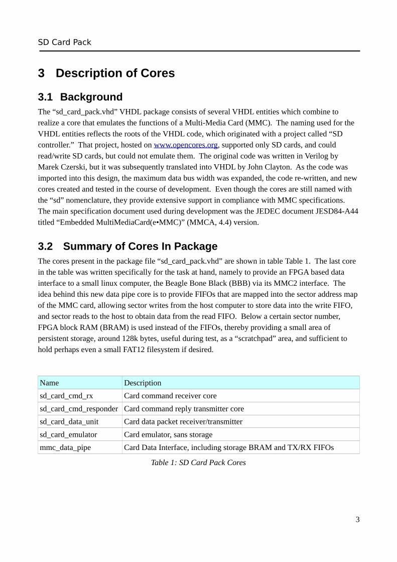
3.2 Summary of Cores In PackageThe cores present in the package file “sd_card_pack.vhd” are shown in table Table 1. The last core in the table was written specifically for the task at hand, namely to provide an FPGA based data interface to a small linux computer, the Beagle Bone Black (BBB) via its MMC2 interface. The idea behind this new data pipe core is to provide FIFOs that are mapped into the sector address mapof the MMC card, allowing sector writes from the host computer to store data into the write FIFO, and sector reads to the host to obtain data from the read FIFO. Below a certain sector number, FPGA block RAM (BRAM) is used instead of the FIFOs, thereby providing a small area of persistent storage, around 128k bytes, useful during test, as a “scratchpad” area, and sufficient to hold perhaps even a small FAT12 filesystem if desired.
Name Description
sd_card_cmd_rx Card command receiver core
sd_card_cmd_responder Card command reply transmitter core
sd_card_data_unit Card data packet receiver/transmitter
sd_card_emulator Card emulator, sans storage
mmc_data_pipe Card Data Interface, including storage BRAM and TX/RX FIFOs
Table 1: SD Card Pack Cores
3

SD Card Pack
3.3 sd_card_cmd_rxThe first core is one of the most elementary and basic, an SD/MMC command receiver. Its internal structure is shown in this block diagram:
This module clocks incoming serial command bits into a 48 bit shift register. It starts when a '0' (start) bit is found, and then shifts in 47 additional bits. The expected format of the command is:
0 1 [index] [arg] [crc] 1
Where:
index = 6 bits
arg = 32 bits
crc = 7 bits
It checks that the second bit is a '1' indicating that the command is from the host to the card. It also checks that the last bit is a '1' (stop) bit. The seven bits immediately prior to the stop bit are checkedusing a CRC-7 code. If any of the checks does not pass, the associated error bits are set, and the cmd_ outputs remain unchanged. If all checks pass, then the newly received command contents are stored into the cmd_ outputs, and the cmd_rx_done_o output is pulsed high for one sd_clk_i cycle.
Note that this receiver runs entirely within the sd_clk_i clock domain. Therefore, care must be taken when using the outputs. A FIFO can form a natural "clock domain boundary crossing" or the user may need to implement other special handshaking to safely transfer signals into a different clock domain.
4
47 bit shift
registerStart bit detector
(coundown load)
6 bit down counter
Command Data
CRC-7 checker
Out
put L
atch
cmd_raw_o
cmd_index_o
cmd_arg_o
(error flags)

SD Card Pack
3.4 sd_card_responderThis core is used to send responses to commands which are received by the sd_card_cmd_receiver. The block diagram of this core is:
This module latches parallel data into a shift register, and then shifts the data out as a command response, using the sd_clk_i input as the clock. The process of sending a response begins when the respond_i input is driven high. The generic N_CR determines how many clocks occur between the respond_i pulse, and the actual start bit of the response. Per the SD/MMC card specifications, thereare two clock periods of tri-state bus "turnaround time" following the stop bit of the command. Theturnaround time is when neither the host nor the card are required to drive the bus, so the stray capacitance on the bus lines briefly holds the previous value that was on the bus, but the voltages are then constantly decaying. Then the card takes over at the end of the turnaround time and begins driving the bus, initially through a pullup resistance, and then when the full N_CR time has expired,with actual response bits. The value of N_CR must not be set below 5 to comply with the minimumvalues in the SD/MMC specification. If the respond_i input occurs in the clock following the command stop bit, then a value of 4 is the lowest permitted N_CR. The sd_cmd_oe_o signal, controlled by the up-counter “n_cr_count” is meant to allow for the accomplishment of the 2 clock turnaround time, but this has been commented out in the current VHDL code. That is because in thecurrent implementation, the response_i input occurs several clocks after the last bit of the incoming command, and so the turnaround time is already accounted for.
5
shift register
8 bit counter
sd_cmd_o
CRC-7 generatordone_o
respond_i
resp_pyld_i
resp_index_i
Mux
sd_cmd_oe_o
sd_clk_i
busy_o

SD Card Pack
According to the SD/MMC card specification, there are several different types of card responses:
Type Length Structure
R1 48 bit "00" & 6 bit index & 32 bit card status & 7 bit CRC & '1'
R2 136 bit "00111111" & 120 bit CID or CSD & 7 bit CRC & '1'
R3 48 bit "00111111" & 32 bit OCR & "11111111"
R4 48 bit "00100111" & 16 bit RCA & 1 bit status & 7 bit reg addr & 8 bit reg read data & 7 bit CRC & '1'
R5 48 bit "00101000" & 16 bit RCA & 16 bit undefined & 7 bit CRC & '1'
Table 2: SD Card Response Types
The length of the shift register is determined by a generic parameter, RESP_PYLD_LEN, accordingto the following formula:
shift_reg_length = 8 + RESP_PYLD_LEN + 8 = 16 + RESP_PYLD_LEN
Thus, for the 48 bit response, RESP_PYLD_LEN is set to 32, and for the 136 bit response, RESP_PYLD_LEN is set to 120.
This module automatically populates the first two bits of the reply with "00", Because all of the replies begin with "00." The next 6 bits are supplied by the "resp_index_i" signal. After that, the next set of bits is supplied by the signal "resp_pyld_i" which stands for "response payload." Since the payload could be either 32 bits or 120 bits long, the payload length is set by the RESP_PYLD_LEN generic.
This module contains a CRC unit which calculates the 7 CRC bits to place at the end, and the final stop bit is also sent out automatically.
Whenever the responder is idle, asserting the respond_i input causes the response to be latched immediately, and the first bit of the newly requested reponse is sent out on the following clock cycle. If a response is already being actively sent out, the respond_i input is simply ignored.
It is envisioned that several instances of the responder may be used in parallel, each being connected to a different SD/MMC card register. Therefore, coordination of the response signals needs to be done in a higher level module, possibly through some sort of data selector or "mux" to
6

SD Card Pack
determine which sd_cmd_o and sd_cmd_oe_o outputs get used, and also perhaps through logic to ensure that only the desired respond_i input is asserted. This may seem somewhat "messy," but it was done with the idea in mind that certain types of responses could be easily left out of the design completely, by eliminating the associated responder instance. The higher level module is also responsible for determining the timing between receipt of a command, and the start of the response.
For instance, the SD/MMC card standard specifies that for identification responses, exactly 5 clock cycles should exist between the stop bit of the command, and the start bit of the response.
Note that this responder runs entirely within the sd_clk_i clock domain. Therefore, care must be taken when supplying the inputs. A FIFO can form a natural "clock domain boundary crossing" or the user may need to implement other special handshaking to safely receive signals from a different clock domain.
7

SD Card Pack
3.5 sd_card_data_unitThis core handles all of the data transactions between the SD/MMC card and the host. A block diagram of the unit is shown here:
This module accepts SD/MMC card data transfers, and generates return transfers for sending data tothe cardbus host. Currently stream based reads and writes are not supported, so if the "continuous_i" input is asserted, the unit remains in IDLE state and does not respond to read, write and bustest requests.
Data transfers in SD/MMC cards begin with a low asserted start bit, followed by data and then a 16-bit CRC code and a high asserted stop bit. In this sense, because the data transfers resemble asynchronous serial transmissions, the sd_card_data_unit could be considered roughly equivalent toeight parallel USARTs which handle characters that are 512+ bits long, with a 16-bit CRC instead of a single parity bit. Since all the data bits are transferred synchronously according to the sd_clk_i input, there is no “asynchronous” nature to it.
The crc_ok_o output indicates the validity of the CRC-16 field of the data received through sd_dat_i.
8
Finite State Machine
dat_reg
CRC-16 generator
CRC-16 generator
CRC-16 generator
CRC-16 generator
CRC-16 generator
CRC-16 generator
CRC-16 generator
CRC-16 generator
transf_cnt (16-bit)
blkcnt_reg
sd_dat_i (8 bits)
dat_muxsd_dat_o (8 bits)
sd_dat_oe_o
tx_dat_i (8 bits)
rx_dat_o (8 bits)
tx_dat_rd_orx_dat_we_o
sd_dat_busy_o
fsm_busy_o
crc_ok_o
blksize_i (12 bits)
bus_size_i (2 bits)
continuous_i
blkcnt_i (16 bits)
bustest_r_ibustest_w_i
d_write_id_read_i
d_stop_i
sd_clk_i
SD Card Pack
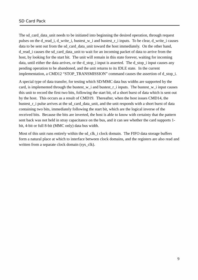
The sd_card_data_unit needs to be initiated into beginning the desired operation, through request pulses on the d_read_i, d_write_i, bustest_w_i and bustest_r_i inputs. To be clear, d_write_i causes data to be sent out from the sd_card_data_unit toward the host immediately. On the other hand, d_read_i causes the sd_card_data_unit to wait for an incoming packet of data to arrive from the host, by looking for the start bit. The unit will remain in this state forever, waiting for incoming data, until either the data arrives, or the d_stop_i input is asserted. The d_stop_i input causes any pending operation to be abandoned, and the unit returns to its IDLE state. In the current implementation, a CMD12 “STOP_TRANSMISSION” command causes the assertion of d_stop_i.
A special type of data transfer, for testing which SD/MMC data bus widths are supported by the card, is implemented through the bustest_w_i and bustest_r_i inputs. The bustest_w_i input causes this unit to record the first two bits, following the start bit, of a short burst of data which is sent out by the host. This occurs as a result of CMD19. Thereafter, when the host issues CMD14, the bustest_r_i pulse arrives at the sd_card_data_unit, and the unit responds with a short burst of data containing two bits, immediately following the start bit, which are the logical inverse of the received bits. Because the bits are inverted, the host is able to know with certainty that the pattern sent back was not held in stray capacitance on the bus, and it can see whether the card supports 1-bit, 4-bit or full 8-bit (MMC only) data bus width.
Most of this unit runs entirely within the sd_clk_i clock domain. The FIFO data storage buffers form a natural place at which to interface between clock domains, and the registers are also read andwritten from a separate clock domain (sys_clk).
9

SD Card Pack
3.6 sd_card_emulatorThis core combines all the lower level units needed in order to emulate the behavior of an SD/MMCdevice. However, boot sectors and DDR transfers are not supported. Instead of a full complement of FLASH based storage cells such as a normal SD/MMC device includes, this core provides a data interface so that outside logic can store and provide data to be used by the card. A block diagram ofthe unit is shown here:
This module does what an SD/MMC card would do, within reason. That is to say, it responds to commands, and accepts and provides data, but it does not contain the actual data storage cells. Instead of storing data directly into a non-volatile memory array, this module provides an addressed parallel bus interface, so that FIFOs or other RAM buffers can be attached and used as storage. Theidea is that entire ranges of addresses can be mapped into the same storage buffer, or a set of bufferswhich are set up on certain address boundaries. With these buffers in place, the sd_card_controller can act as a "bridge" between a host system and the FIFOs. Data can be transferred to and from the FIFO buffers, all the while the host system believes it is communicating with an SD or MMC card.
Obviously, this scheme does not include the concept of a file system, which therefore necessitates the use of a host command which can read and write to specific SD/MMC sectors, which are most often 512 bytes each in length. For Linux hosts, there exists a command, namely the "dd" command, which can serve to access individual sectors. An example of this command being issued from the Linux command line is given below, along with debug output shown after the command, helping to illustrate the sequence of SD/MMC commands and responses which occur as part of the
10
Finite State
Machine
sd_card_cmd_rx
sd_card_respondersd_card_respondersd_card_respondersd_card_respondersd_card_responder
sd_card_data_handler
Card Registers
EXT_CSD RAM
sd_cmd_i
sd_cmd_o
Bus interface
sd_cmd_oe_o
sd_od_mode_o
SD Data Signals Interface
to Data FIFOs
and RAM

SD Card Pack
transfer:
WRITE BLOCK 0 : dd if=/dev/zero of=/dev/mmcblk1 bs=4k count=1
Jan 15 11:45:31 bbb user.debug kernel: [ 253.042114] omap_hsmmc 481d8000.mmc: enabled
Jan 15 11:45:31 bbb user.debug kernel: [ 253.042235] omap_hsmmc 481d8000.mmc: mmc1: CMD25, argument 0x00000000
Jan 15 11:45:31 bbb user.debug kernel: [ 253.042274] omap_hsmmc 481d8000.mmc: IRQ Status is 1
Jan 15 11:45:31 bbb user.debug kernel: [ 253.096448] omap_hsmmc 481d8000.mmc: IRQ status is 2
Jan 15 11:45:31 bbb user.debug kernel: [ 253.096478] omap_hsmmc 481d8000.mmc: mmc1: CMD12, argument 0x00000000
Jan 15 11:45:31 bbb user.debug kernel: [ 253.096511] omap_hsmmc 481d8000.mmc: IRQ Status is 3
Jan 15 11:45:31 bbb user.debug kernel: [ 253.096617] omap_hsmmc 481d8000.mmc: mmc1: CMD13, argument 0x00010000
Jan 15 11:45:31 bbb user.debug kernel: [ 253.096640] omap_hsmmc 481d8000.mmc: IRQ Status is 1
Jan 15 11:45:31 bbb user.debug kernel: [ 253.195201] omap_hsmmc 481d8000.mmc: disabled
From the above command, we can see that a block of 4K bytes was being written, starting at sector 0x00000000. The CMD25 is an eMMC “Write Multiple Block” command, where the argument is the starting sector of the transfer. Then, the CMD12 is the “Stop Transmission” command issued bythe host after it has written the eight sectors that comprise the 4K byte block of data, and finally the CMD13 is a “Send Status” command.
This SD/MMC card emulator can implement all of the response types shown in Table 2. There is a "modified" R1 response, called R1b, in which the D0 line can be held low to signify that the card needs more time because it is busy. Currently, the R1b option to delay is not implemented by the R1 responder unit that is instantiated inside the sd_card_emulator. However, the practice of holdingD0 low to indicate card busy status is implemented by both the sd_card_data_unit and by a special “programming emulation” delay implemented in the state machine of the sd_card_emulator. For the sd_card_data_unit, busy indication is given whenever the card is receiving data, and a new sector is being “written” into FLASH. This delay is set by the generic BLK_PRG_TIME on the sd_card_data_unit. The delay implemented in sd_card_emulator is to cover other types of card delay. Busy delays implemented by the sd_card_emulator are summarized in Table 3.
Time (eMMC clks) Structure
200 Sector programming busy time, implemented by sd_card_data_unit
4000 CMD6 (“SWITCH”) delay time
4000 CMD28 (“SET_WRITE_PROT”) delay time
4000 CMD29 (“CLR_WRITE_PROT”) delay time
4000 CMD38 (“ERASE”) delay time
4000 CMD7 (“SELECT”) emerging from CARD_INA delay time
Table 3: SD Card Busy Delay Times
11

SD Card Pack
Note that for CMD28, CMD29 and CMD38, the sd_card_emulator does not actually do anything besides giving a busy delay indication back to the host. For example, when commanded to ERASE sectors, the sd_card_emulator currently does not issue bus cycles or signals to cause the storage to actually be erased. If the user desires to modify the busy delays, there is no constant or generic parameter to use because the delays are currently “hard coded” for each case. Simply search through the VHDL code for the number, and these settings can be found.
The R4 and R5 card response types are optional, according to the eMMC specification, and they canbe de-selected by setting the USE_R4_RESPONSE and USE_R5_RESPONSE generics to zero.
Boot modes are not supported, although they probably could be with a modicum of additional work.The states are already provided in the card state machine, along with some comments detailing whatneeds to be done.
This module assumes it is the only card on the host SD/MMC card bus. Therefore, it does not "bitwise monitor its outgoing bitstream" when responding to ALL_SEND_CID (CMD2). See eMMC Specification JESD84-A44, section 7.4.5 "Card Identification Process" for further details.
In the sd_card_emulator, there are “card registers” and “module registers.” This distinction is madefor clarity when discussing the structure and operation of the sd_card_emulator. The six card registers are summarized in Table 4. Further technical details about these registers can be found in the eMMC Specification JESD84-A44, section 8, “Card registers.”
12

SD Card Pack
Acronym Notes
OCR The 32-bit operation conditions register (OCR) stores the VDD voltage profile of the card and the access mode indication.
CID The 128-bit Card IDentification (CID) register contains the card identification information used during the card identification phase (MultiMediaCard protocol). Each card has a unique CID.
CSD The 128-bit Card-Specific Data (CSD) register provides information on how to access the card contents. The CSD defines the data format, error correction type, maximum data access time, data transfer speed, whetherthe DSR register can be used etc. sd_card_emulator does not implementprogramming this register via eMMC commands, but it does implement full programmability of it via system bus module register access.
EXT_CSD The 512 byte long Extended CSD register defines the card properties and selected modes. The most significant 320 bytes are the Properties segment, which defines the card capabilities and cannot be modified by the host. The lower 192 bytes are the Modes segment, which defines the configuration the card is working in. These modes can be changed by the host by means of the SWITCH command, which is fully implemented by the sd_card_emulator. Read/write access to the entire EXT_CSD contents is given via the system bus using module registers.
RCA The writable 16-bit relative card address (RCA) register carries the card address assigned by the host during the card identification. This address is used for the addressed host-card communication after the card identification procedure. The default value of the RCA register is 0x0001. The value 0x0000 is reserved to set all cards into the Stand-by State with CMD7.
DSR The 16-bit driver stage register (DSR) can be optionally used to improvethe bus performance for extended operating conditions (depending on parameters like bus length, transfer rate or number of cards). The CSD register carries the information about the DSR register usage. The default value of the DSR register is 0x404. Although the sd_card_emulator does not modify its transceiver performance parameters in response to this register, it does implement the register.
Table 4: Summary of card registers
13

SD Card Pack
Several of the card registers are accessible via the system registers, some with full read/write access, and some with read only or partial write access. In addition, a system register was allocated for counting the number of CRC errors found in commands received by the sd_card_emulator, but this function has not yet been implemented. The module registers are summarized in Table 5.
Address Structure
0x0 Card Status (reported)
0x1 RCA in bits 31..16, DSR in bits 15..0
0x2 EXT_CSD address, in bits 8..0
0x3 EXT_CSD data, in bits 7..0
0x4 CSD(31:0)
0x5 CSD(63:32)
0x6 CSD(95:64)
0x7 CSD(127:96)
0xF SD command CRC error count. Write to clear. (Not implemented)
Table 5: Summary of module registers
In order to use the sd_card_emulator effectively, it is helpful to have a more detailed understanding of the individual fields contained within the registers. Each register is provided with its own detailed diagram, showing the bits which are implemented versus those which are not implemented,and giving the names of the fields and bits. Also, the access mode is shown, and the default value isgiven in binary within the diagram.
Register 0x0 : Card Status
The card status register is not implemented fully as it is in a real card. However, full access to the register is given through the system register interface, so that apart from the read only fields, any desired value can be written into it.
14

SD Card Pack
The meaning of the values in the card state field are shown in Table 6.
Value Name Meaning
0x0 CARD_IDLE Card is idle (default power on state)
0x1 CARD_READY Card competes for the bus, while sending its CID
0x2 CARD_IDENT Card is waiting to be assigned a relative address (RCA)
0x3 CARD_STBY Card is awaiting general commands
0x4 CARD_TRAN Card is selected, awaiting transfer command
0x5 CARD_DATA Card is sending data to host
0x6 CARD_RCV Card is receiving data from host
0x7 CARD_PRG Card is programming data into flash storage
0x8 CARD_DIS Card is disabled
0x9 CARD_BTST Card is doing bus test operations
0xA CARD_SLP Card is in sleep mode
0xB (others) Illegal states, should not occur
Table 6: Card State Values
15
Addr: 0x0 Access: Read/Write (*Fields are read only)
crc_
err_
repl
y*
cmd_
err_
repl
y*
read
y_fo
r_da
ta*
status(31:24) status(21:13) card state* status(7:0)0 0 0 0 0 0 0 0 0 0 0 0 0 0 0 0 0 0 0 0 0 0 0 1 0 0 0 0 0 0 0 031 0

SD Card Pack
Register 0x1 : RCA, DSR
The Relative Card Address (RCA) and Driver Stage Register (DSR) are packed into a single systemregister.
The default values have been set according to the normal card defaults, as described in the eMMC specification. The DSR is not used to alter the behavior of any drivers in the design, but it still exists as a register that can be written by a host sending CMD4, SET_DSR. The RCA can be written by a host sending CMD3, SET_RELATIVE_ADDRESS. This register has the Read Only access mode because it cannot be written using the system bus.
Register 0x2 : EXT_CSD address
An indirect addressing approach is used to read and alter the contents of the EXT_CSD ram, which contains 512 bytes of information. This register contains the 9-bit address of the desired byte, and then register 0x3 is used to read or write the selected data byte.
During development of the sd_card_emulator, two different cards were tested, and the EXT_CSD was read out of both. It was found that most of the bytes contained 0x00. The non-zero bytes are shown in Table 7.
16
Addr: 0x1 Access: Read Only
Relative Card Address (RCA) Driver Stage Register (DSR)0 0 0 0 0 0 0 0 0 0 0 0 0 0 0 1 0 0 0 0 0 1 0 0 0 0 0 0 0 1 0 031 0
Addr: 0x2 Access: Read/Write
address0 0 0 0 0 0 0 0 0 0 0 0 0 0 0 0 0 0 0 0 0 0 0 0 0 0 0 0 0 0 0 031 0

SD Card Pack
EXT_CSDAddress
Field Name Pretec CardContents
Transcend CardContents
0xB7 BUS_WIDTH 0x02 0x02
0xC0 EXT_CSD_REV 0x00 0x01
0xC2 CSD_STRUCTURE 0x03 0x02
0xC4 CARD_TYPE 0x03 0x03
0xD7-D4 SEC_COUNT 0x0078F800 0x00000000
Table 7: EXT_CSD Non-Zero Values
Since the Pretec card is less than 2GB, it has a storage capacity that is determined by the contents ofthe CSD register, specifically the C_SIZE, C_SIZE_MULT and READ_BL_LEN fields, according to a formula given in the eMMC specification. The Transcend card, on the other hand, is greater than 2GB, so its capacity is given by the EXT_CSD SECTOR_COUNT field. Briefly, the value 0x0078F800 = 7,927,808 sectors. Each sector is 512 bytes in length, equaling 4,059,037,696 bytes. This is somewhat less than 4GB = 2^32 bytes = 4,294,967,296. It’s not very far off, actually about 5.5% less than the full 4GB capacity.
17

SD Card Pack
Register 0x3 : EXT_CSD data
This register is the “window” through which the particular EXT_CSD byte, selected by the EXT_CSD address register, is accessed.
According to the specification, only values in the “properties segment” of the EXT_CSD, which begins at byte 192 and extends through byte 512, are able to be written through card commands. However, via the system bus all bytes in the EXT_CSD of the sd_card_emulator can be written at any time.
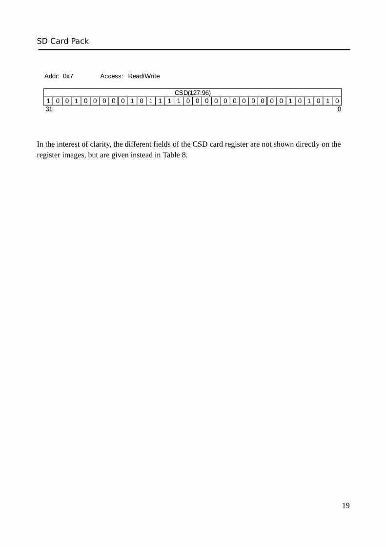
Registers 0x4 – 0x7 : CSD
These four registers contain the bits of the single 128-bit card register called CSD.
18
Addr: 0x3 Access: Read/Write
ext_csd data byte0 0 0 0 0 0 0 0 0 0 0 0 0 0 0 0 0 0 0 0 0 0 0 0 0 0 0 0 0 0 0 031 0
Addr: 0x4 Access: Read/Write
CSD(31:0)1 0 0 1 0 1 1 0 0 1 0 0 0 0 0 0 0 0 0 0 0 0 0 0 0 0 0 0 0 0 0 031 0
Addr: 0x5 Access: Read/Write
CSD(63:32)1 1 1 0 1 1 0 1 1 0 1 1 0 1 1 1 0 0 0 0 0 1 1 1 1 1 1 1 1 1 1 131 0
Addr: 0x6 Access: Read/Write
CSD(95:64)0 0 0 1 1 1 1 1 0 1 0 1 1 0 0 1 0 0 0 0 0 0 1 1 1 1 0 1 0 0 1 131 0
SD Card Pack
In the interest of clarity, the different fields of the CSD card register are not shown directly on the register images, but are given instead in Table 8.
19
Addr: 0x7 Access: Read/Write
CSD(127:96)1 0 0 1 0 0 0 0 0 1 0 1 1 1 1 0 0 0 0 0 0 0 0 0 0 0 1 0 1 0 1 031 0

SD Card Pack
CSD bits Field Name Description
[127:126] CSD_STRUCTURE CSD structure
[125:122] SPEC_VERS System specification version
[121:120] - Reserved
[119:112] TAAC Data read access-time 1
[111:104] NSAC Data read access-time 2
in CLK cycles (NSAC*100)
[103:96] TRAN_SPEED Max. bus clock frequency
[95:84] CCC Card command classes
[83:80] READ_BL_LEN Max. read data block length
[79:79] READ_BL_PARTIAL Partial blocks for read allowed
[78:78] WRITE_BLK_MISALIGN Write block misalignment
[77:77] READ_BLK_MISALIGN Read block misalignment
[76:76] DSR_IMP DSR implemented
[75:74] - Reserved
[73:62] C_SIZE Device size
[61:59] VDD_R_CURR_MIN Max. read current @ VDD min
[58:56] VDD_R_CURR_MAX Max. read current @ VDD max
[55:53] VDD_W_CURR_MIN Max. write current @ VDD min
[52:50] VDD_W_CURR_MAX Max. write current @ VDD max
[49:47] C_SIZE_MULT Device size multiplier
[46:42] ERASE_GRP_SIZE Erase group size
[41:37] ERASE_GRP_MULT Erase group size multiplier
[36:32] WP_GRP_SIZE Write protect group size
[31:31] WP_GRP_ENABLE Write protect group enable
20

SD Card Pack
[30:29] DEFAULT_ECC Manufacturer default ECC
[28:26] R2W_FACTOR Write speed factor
[25:22] WRITE_BL_LEN Max. write data block length
[21:21] WRITE_BL_PARTIAL Partial blocks for write allowed
[20:17] - Reserved
[16:16] CONTENT_PROT_APP Content protection application
[15:15] FILE_FORMAT_GRP File format group
[14:14] COPY Copy flag (OTP)
[13:13] PERM_WRITE_PROTECT Permanent write protection
[12:12] TMP_WRITE_PROTECT Temporary write protection
[11:10] FILE_FORMAT File format
[9:8] ECC ECC code
[7:1] CRC 7 CRC
[0:0] - Not used, always’1’
Table 8: CSD Fields
For further details about the nature and use of these fields, please refer to eMMC specifications.
21

SD Card Pack
3.7 mmc_data_pipeThis core combines an sd_card_emulator, with a small amount of RAM, mapped to lower sector numbers, and TX and RX FIFOs mapped to higher sectors. A parallel bus interface enables control of the unit. The sd_card_emulator operates in the sd_clk_i clock domain, so dual ported block RAMs are used for the RAM and FIFOs in order to enable the data to safely cross into the system clock domain. The core is parameterized, so that the sizes of the RAM and the TX/RX FIFOs can be adjusted according to the resources available within the target device. A block diagram of the core is given here:
The use of the Parallel System Bus interface is optional, and the entire interface can be left disconnected, as long as the default register settings and generic settings are set up for the needed operation.
The FIFO_DEPTH integer generic sets the size of the FIFO buffers. Default setting is 2048 bytes, but other sizes can be used depending on the number of block RAMs available within the FPGA.
The MMC_RAM_ADR_BITS integer generic sets the size of the address bus feeding to the Data Block RAM, and hence the size of the actual RAM itself. In testing, the value of 17 has been used, resulting in 128k bytes of Data Block RAM available. Since the size of a sector is 512 bytes, there are 256 sectors available in the 128k block of RAM. Any card write to sector 256 or above sends the data to the Write FIFO (“TX FIFO”). Any card read from sector 256 or above reads the data from the Read FIFO (“RX FIFO”).
The TX and RX FIFOs cross from the SD/MMC card clock domain, into the FPGA system clock domain, which makes this core function as a sort of “data pipe” through which information can be passed to the host system, over SD/MMC signaling.
There are no additional registers inside the mmc_data_pipe core. The sd_card_emulator registers are all available over the parallel system bus.
22
Opcode Data ready to process
DataBlock RAM
sd_card_emulator
Write FIFO
Read FIFO
Parallel System Bus interface
Status Data ready to read
R/W RAM Access
SD/MMC bus