scilab textbook companion for integrated circuits by k. r
TRANSCRIPT

Scilab Textbook Companion forIntegrated Circuitsby K. R. Botkar1
Created byTushar Kashyap
B.TECHElectronics Engineering
Model Engineering CollegeCollege Teacher
Ms.Vineetha George E, Model Engineering CollegeCross-Checked by
Ms. Vineetha George E
July 31, 2019
1Funded by a grant from the National Mission on Education through ICT,http://spoken-tutorial.org/NMEICT-Intro. This Textbook Companion and Scilabcodes written in it can be downloaded from the ”Textbook Companion Project”section at the website http://scilab.in

Book Description
Title: Integrated Circuits
Author: K. R. Botkar
Publisher: Khanna Publishers
Edition: 5
Year: 2010
ISBN: 81-7409-208-0
1
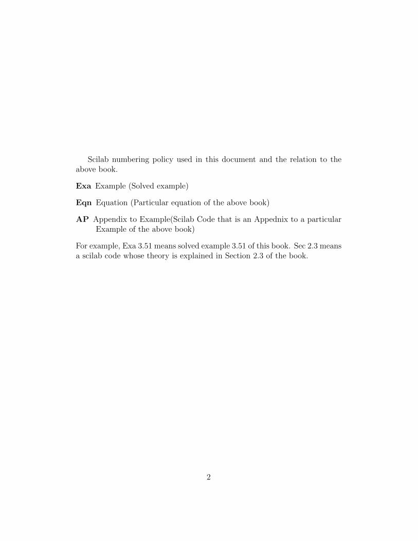
Scilab numbering policy used in this document and the relation to theabove book.
Exa Example (Solved example)
Eqn Equation (Particular equation of the above book)
AP Appendix to Example(Scilab Code that is an Appednix to a particularExample of the above book)
For example, Exa 3.51 means solved example 3.51 of this book. Sec 2.3 meansa scilab code whose theory is explained in Section 2.3 of the book.
2

Contents
List of Scilab Codes 4
2 Thick Film And Thin Film Hybrid ICs 5
3 Semoconductor Devices Fundamentals 13
5 Monolithic Components 18
7 Operational Amplifier Characteristics 22
8 Applications of Operational Amplifier 30
9 Active Filters 35
10 Special Purpose Amplifiers 37
11 Nonlinear Circuit Application 43
12 Signal Generators 46
13 Voltage Regulators 51
15 Phase Locked Loops 54
16 Bipolar and MOS Digital Gate Circuits 59
3

17 Light Emitting Diodes and Liquid Crystal Displays 65
4

List of Scilab Codes
Exa 2.1 Resistance . . . . . . . . . . . . . . . . . . . 5Exa 2.2 Resistance Calculation . . . . . . . . . . . . 6Exa 2.3 Sheet Resistivity . . . . . . . . . . . . . . . 7Exa 2.4 Design Capacitor . . . . . . . . . . . . . . . 7Exa 2.6 Capacitance . . . . . . . . . . . . . . . . . . 8Exa 2.8 Thickness . . . . . . . . . . . . . . . . . . . 9Exa 2.9 Length . . . . . . . . . . . . . . . . . . . . . 9Exa 2.10 Absolute Coefficient . . . . . . . . . . . . . 10Exa 2.11 Ratio . . . . . . . . . . . . . . . . . . . . . . 11Exa 3.2 Resistivity . . . . . . . . . . . . . . . . . . . 13Exa 3.3 Resistivity of Intrinsic Ge . . . . . . . . . . 14Exa 3.4 Hole Concentration . . . . . . . . . . . . . . 14Exa 3.5 Resistivity of Cu . . . . . . . . . . . . . . . 15Exa 3.6 Bipolar Transistor Parameters . . . . . . . . 15Exa 5.1 Transit Time . . . . . . . . . . . . . . . . . 18Exa 5.2 Unit gain frequency . . . . . . . . . . . . . . 19Exa 5.3 Resistance and Sheet resistance . . . . . . . 19Exa 5.4 Capacitance per unit area . . . . . . . . . . 20Exa 7.1 Bipolar Differential Amplifier Parameter . . 22Exa 7.2 Rc and Re . . . . . . . . . . . . . . . . . . . 23Exa 7.4 Offset Voltage Change . . . . . . . . . . . . 24Exa 7.5 Temperature Coefficient . . . . . . . . . . . 25Exa 7.14 Effect on Output Voltage . . . . . . . . . . 26Exa 7.15 Slew rate and Fmax . . . . . . . . . . . . . 27Exa 7.16 Largest Amplitude . . . . . . . . . . . . . . 27Exa 7.17 Maximum allowable frequency . . . . . . . . 28Exa 8.1 Device Temperature . . . . . . . . . . . . . 30Exa 8.2 Device Temperature . . . . . . . . . . . . . 31
5

Exa 8.3 Device Temperature . . . . . . . . . . . . . 31Exa 8.4 Device Temperature . . . . . . . . . . . . . 32Exa 8.7 Output Voltage . . . . . . . . . . . . . . . . 32Exa 8.8 Vp and Vo . . . . . . . . . . . . . . . . . . . 33Exa 9.6 Determine Q Fl and Fh . . . . . . . . . . . 35Exa 9.12 Unity gain frequency and Capacitor determi-
nation . . . . . . . . . . . . . . . . . . . . . 35Exa 10.3 Class B Power Amplifier . . . . . . . . . . . 37Exa 10.4 Power Output . . . . . . . . . . . . . . . . . 38Exa 10.8 LM4250 Parameters . . . . . . . . . . . . . 39Exa 10.9 Common Emitter Amplifier Parameters . . . 40Exa 11.4 Time taken . . . . . . . . . . . . . . . . . . 43Exa 11.5 Rise Time . . . . . . . . . . . . . . . . . . . 43Exa 11.11 Design Peak Detector . . . . . . . . . . . . . 44Exa 12.6 555 Timer . . . . . . . . . . . . . . . . . . . 46Exa 12.11 Design . . . . . . . . . . . . . . . . . . . . . 47Exa 12.12 Generating pulse by 555 timer . . . . . . . . 47Exa 12.20 Waveform Generator . . . . . . . . . . . . . 49Exa 13.3 Maximum Efficiency and Power . . . . . . . 51Exa 13.14 Inductor and Capacitor . . . . . . . . . . . 52Exa 15.2 Output Signal Frequency . . . . . . . . . . . 54Exa 15.3 VCO and Phase detector . . . . . . . . . . . 55Exa 15.4 Second Order Butterworth Filter . . . . . . 56Exa 15.5 Lock Range . . . . . . . . . . . . . . . . . . 57Exa 16.2 Noise Margin . . . . . . . . . . . . . . . . . 59Exa 16.3 Fanouts . . . . . . . . . . . . . . . . . . . . 60Exa 16.12 NMOS operating region . . . . . . . . . . . 61Exa 16.13 Power Dissipation . . . . . . . . . . . . . . . 62Exa 16.14 AC Power . . . . . . . . . . . . . . . . . . . 63Exa 17.2 Viewing distance . . . . . . . . . . . . . . . 65
6

Chapter 2
Thick Film And Thin FilmHybrid ICs
Scilab code Exa 2.1 Resistance
1 // Chapter 2 Th ick Film and Thin Film Hybrid ICs2 // Capt ion : R e s i s t a n c e3 // Example2 . 1 : a ) A r e s i s t o r has an a s p e c t r a t i o o f
2 0 : 1 and s h e e t r e s i s t a n c e o f 200 ohm/ squa r e . Findout the v a l u e o f r e s i s t a n c e .
4 // b ) Find out the number o f s q u a r e s c o n t a i n e d i n a2 k i loohm r e s i s t o r whose s h e e t r e s i s t a n c e i s 200ohm per squa r e .
5 // S o l u t i o n : a )6 clear;
7 clc;
8 function y= myfunction(x,z)//y : r e s i s t a n c e , x : s h e e tr e s i s t a n c e =200ohm/ square , z : a s p e c t r a t i o =20:1
9 y = x*z // s i n c e , r e s i a t a n c e=s h e e t r e s i s t a n c e10 disp( ’ r e s i s t a n c e i s =”)11 d i s p ( ’ ohm ’,y)12 endfunction
13
14 // S o l u t i o n : b )
7

15 // we have to f i n d number o f s qua r e which i s to f i n da s p e c t r a t i o .
16 function s=myfunction1(r,p)// r : r e s i s t o r =2kohm ( or2000ohm) , p : s h e e t r e s i s t a n c e =200 Ohm/ square , s :number o f s qua r e ( a s p e c t r a t i o )
17 s=r/p// s i n c e , number o f s qua r e =( r e s i s t o r / s h e e tr e s i s t a n c e )
18 disp( ’ number o f s q u a r e s a r e =”) // i n c l u d e ” ; ” at thet ime o f c a l l i n g the f u n c t i o n
19 d i s p ( ’ squares ’,s)20 endfunction
21 // myfunct ion ( 2 0 0 , 2 0 / 1 ) ; myfunct ion1 ( 2 0 0 0 , 2 0 0 ) ;
Scilab code Exa 2.2 Resistance Calculation
1 // Chapter 2 Th ick Film and Thin Film Hybrid ICs2 // Capt ion : R e s i s t a n c e c a l c u l a t i o n3 // Example2 . 2 : A t h i c k f i l m r e s i s t o r i s s c r e e n e d with
a p a s t e o f f s h e e t r e s i s t i v i t y 10000 ohm/ square ,and the r e s i s t o r i s d e f i n e d as 0 . 2 4 cm long and0 . 0 6 cm wide . C a l c u l a t e the r e s i s t a n c e R.
4 // S o l u t i o n :5 clear;
6 clc;
7 function R=myfunction3(p,l,w)// r : r e s i s t o r , p=s h e e tr e s i s t a n c e =10000 ohm/ square , l : l e n g t h o f r e s i s t o r=0.24cm , w: width o f the r e s i s t o r =0.06cm
8 R=p*(l/w)// s i n c e , r e s i s t a n c e=s h e e t r e s i s t a n c e ∗ (l e n g t h o f r e s i s t o r / width o f the r e s i s t o r )
9 disp( ’ r e s i s t a n c e o f the t h i c k f i l m r e s i s t o r i s= ’)// at the t ime o f c a l l i n g the f u n c t i o ni n c l u d e ” ; ” a f t e r i t
10 disp( ’ ohm ’ ,R)11 endfunction
12 // myfunct ion3 ( 1 0 0 0 0 , 0 . 2 4 , 0 . 0 6 ) ;
8

Scilab code Exa 2.3 Sheet Resistivity
1 // Chapter 2 Th ick Film and Thin Film Hybrid ICs2 // Capt ion : Shee t R e s i s t i v i t y3 // Example2 . 3 : C a l c u l a t e the s h e e t r e s i s t i v i t y o f a
squa r e o f t h i c k f i l m r e s i s t o r m a t e r i a l with thef o l l o w i n g p r o p e r t i e s : bu lk r e s i s t i v i t y =10ˆ−1ohm−cm and t h i c k f i l m t h i c k n e s s =10 micrometer .
4 // S o l u t i o n :5 clear;
6 clc;
7 function Ps=myfunction4(p,t)// Ps : s h e e t r e s i s t a n c e ,p : bu lk r e s i s t i v i t y o f t h i c k f i l m =10ˆ−1( or 0 . 0 1 ) ,t : t h i c k n e s s o f t h i c k f i l m =10 micrometer(=10∗10ˆ−4=0.001)
8 Ps=p/t// s i n c e , s h e e t r e s i s t a n c e o f the f i l m=bulk r e s i s t a n c e o f the f i l m / t h i c k n e s s o f thef i l m
9 disp( ’ s h e e t r e s i s t i v i t y i s= ’ )// i n c l u d e ” ; ” a t a tthe t ime o f c a l l i n g the f u n c t i o n
10 disp( ’ ohm per squa r e ’ ,Ps)11 endfunction
12 // myfunct ion4 (10ˆ−1 ,10∗10ˆ−4) ;
Scilab code Exa 2.4 Design Capacitor
1 // Chapter 2 Th ick Film and Thin Film Hybrid ICs2 // Capt ion : Des ign C a p ac i t o r3 // Example2 . 4 : Des ign a c i r c u l a r 100pF c a p a c i t o r with
the t h i c k f i l m d i e l e c t r i c hav ing d i e l e c t r i c f i l mt h i c k n e s s =0.02mm( or 0 . 0 0 2 cm) , assume Er=100
9

4 // S o l u t i o n : We have to f i n d the r a d i u s o f c r c u l a rc a p a c i t o r i n o r d e r to d e s i g n i t .
5 clear;
6 clc;
7 function r1= myfunction5(c,t)
8 r1=c*t// c o n s t a n t=c a p a c i t o r ∗ t h i c k n e s s o f t h i c kf i l m
9 Er=100 // g i v e n r e l a t i v e p e r m e a b i l i t y o f t h i c kf i l m
10 r=sqrt(r1/(Er*%pi *8.85*10^ -12))// r a d i u s o fc i r c u l a r c a p a c i t o r , Eo=8 ,85∗10ˆ−12( d i e l e c t r i c
c o n s t a n t o f f r e e space )11 disp( ’ r a d i u s o f c i r c u l a r c a p a c i t o r i s= ’ )//
i n c l u d e ” ; ” at the t ime o f c a l l i n g thef u n c t i o n
12 disp( ’ meter ’ ,r)13 endfunction
14 // myfunct ion5 (100∗10ˆ −12 ,0 .002) ;
Scilab code Exa 2.6 Capacitance
1 // Chapter 2 Th ick Film and Thin Film Hybrid ICs2 // Capt ion : Capac i t ance3 // Example2 . 6 : Find out the c a p a c i t a n c e o f a t h i c k
f i l m c a p a c i t o r , i f the d i e l e c t r i c c o n s t a n t Er =100 ,d i e l e c t r i c f i l m t h i c k n e s s =25 micrometer and a r ea A=0.0625 cm squa r e .
4 // S o l u t i o n :5 clear;
6 clc;
7 function c=capacitance(Er,A,t)
8 c=8.8*10^ -12* Er*A/(10^ -12*t)// c a p a c i t a n c e v a l u ew i l l be 2.2∗10ˆ−10 or 220pF , Eo : d i e l e c t r i c
c o n s t a n t o f f r e e space =8.8∗10ˆ−12 , Er :d i e l e c t r i c c o n s t a n t o f t h i c k f i l m= 100( g i v e n )
10

, A: a r ea o f t h i c k f i l m =0.0626 cm squa r e ( or0.0625∗10ˆ−4m squa r e ) , t : t h i c k n e s s o f thet h i c k f i l m= 25∗10ˆ−6m)
9 // c a p a c i t a n c e=Eo∗Er∗A/ t10 disp( ’ c a p a c i t a n c e i s= ’ )// c =2.200D
−10(=2.2∗10ˆ−10)F , i n c l u d e ” ; ” at l a s t at thet ime o f c a l l i n g the f u n c t i o n
11 disp( ’ pF ’ ,c)//pF : p i c o Farad12 endfunction
13 // c a p a c i t a n c e (100 ,0 .0625∗10ˆ−4 ,25∗10ˆ−6) ;
Scilab code Exa 2.8 Thickness
1 // Chapter 2 Th ick Film and Thin Film Hybrid ICs2 // Capt ion : Th i ckne s s3 // Example2 . 8 : The bulk r e s i s t i v i t y o f nichrom i s 120
uohm−cm . C a l c u l a t e the t h i c k n e s s T i n angst romso f a f i l m with s h e e t r e s i s t i v i t y o f 100ohm/ squa r e.
4 // S o l u t i o n :5 function T=thickness(Ps,p)// Ps : s h e e t r e s i s t i v i t y
o f nichrom =100ohm/ square , p : bu lk r e s i s t i v i t y o fnichrom =120uohm−cm
6 T=p/(Ps*10^ -8) // s i n c e Ps=p/T and 1 angstrom=10ˆ−8cm , so d i v i d i n g by 10ˆ−8 he r e
7 disp( ’ t h i c k n e s s i s= ’ )// i n c l u d e ” ; ” at the t imeo f c a l l i m g the f u n c t i o n
8 disp( ’ angstrom ’ ,T)9 endfunction
10 // t h i c k n e s s (100 ,120∗10ˆ−6) ;
Scilab code Exa 2.9 Length
11

1 // Chapter 2 Th ick Film and Thin Film Hybrid ICs2 // Capt ion : Length3 // Rxample2 . 9 : C a l c u l a t e the l e n g t h o f a 400ohm t h i n
f i l m r e s i s t o r . Given a s h e e t r e s i s t i v i t y o o f 100ohm/ squa r e and a r e s i s t o r width o f 100um
4 // S o l u t i o n :5 clear;
6 clc;
7 function L=extent(r,w,Ps)// L : l e n g t h o f t h i n f i lm , r: r e s i s t a n c e o f t h i n f i l m =400ohm , w: width o fr e s i s t o r =100um, Ps : s h e e t r e s i s t a n c e =100ohm/ squa r e
8 L=r*w/(10^ -6*Ps)// s i n c e , r=Ps∗L/w and l e n g t h i nmicrometer so d i v i d i n g by 10ˆ−6.
9 disp( ’ l e n g t h o f t h i n f i l m i s= ’ )// i n c l u d e ” ; ” atthe t ime o f c a l l i n g the f u n c t i o n at l a s t
10 disp( ’ mic rometer ’ ,L)11 endfunction
12 // e x t e n t (400 ,100∗10ˆ −6 ,100) ;
Scilab code Exa 2.10 Absolute Coefficient
1 // Chapter 2 Th ick Film and Thin Film Hybrid ICs2 // Capt ion : Abso lu te C o e f f i c i e n t3 // Example2 . 1 0 :A t h i n f i l m r e s i s t o r measures 150 ohmat
25 d e g r e e c e l c i u s and 1 5 1 . 5 ohm at 100 d e g r e ec e l c i u s . C a l c u l a t e i t s a b s o l u t e c o e f f i c i e n t o fr e s i s t a n c e i n p a r t s per m i l l i o n (ppm) per deg r ec e l c i u s .
4 // S o l u t i o n :5 clear;
6 clc;
7 function TCR=absresistor(Rt1 ,Rt2 ,T1,T2)// TCR:a b s o l u t e t empera tu r e c o e f f i c i e n t o f r e s i s t a n c e ,Rt1 : r e s i s t a n c e at 100 d e g r e e c e l c i u s =150ohm , Rt2 :r e s i s t a n c e at 25 d e g r e e c e l c i u s =151.5ohm , T1 :
12

t empera tu re =100 d e g r e e c e l c i u s , T2 : t empera tu r e =25d e g r e e c e l c i u s
8 TCR=(Rt2 -Rt1)*10^6/( Rt1*(T1 -T2))
9 disp( ’ a b s o l u t e c o e f f i c i e n t o f r e s i s t a n c e i s =”) //i n c l u d e ” ; ” at the t ime o f c a l l i n g the
f u n c t i o n at l a s t10 d i s p ( ’ ppm/degree Celsius ’,TCR)// ppm : pa r t per
m i l l i o n11 endfunction
12 // a b s r e s i s t o r ( 1 5 0 , 1 5 1 . 5 , 1 0 0 , 2 5 ) ;
Scilab code Exa 2.11 Ratio
1 // Chapter 2 Th ick Film and Thin Film Hybrid ICs2 // Capt ion : Rat io3 // Example2 . 1 1 : Two t h i n r e s i s t o r a r e measured at 50
d e g r e e c e l c i u s and 100 d e g r e e c e l s i u s and a r efound to have the f o l l o w i n g v a l u e s :
4 // Temperatur ( d e g r e e C) Ra(ohm)Rb(ohm)
5 // 50 50100
6 // 100 511 0 2 . 1
7 // C a l c u l l a t e the r a t i o TCR i n ppm/ d e g r e e c e l c i u s .8 // S o l u t i o n :9 function TCR= ratio(Rat1 ,Rbt1 ,Rat2 ,Rbt2 ,T1,T2)
10 TCR=(Rat2/Rbt2 -Rat1/Rbt1)*10^6/(( Rat1/Rbt1)*(T1 -
T2))
11 disp( ’ r a t i o TCR i s =”) // i i n c l u d e ” ; ” at the t imeo f c a l l i n g the f u n c t i o n at l a s t
12 d i s p ( ’ ppm/degree Celsius ’,TCR)//ppm : pa r t perm i l l i o n
13 endfunction
14 // r a t i o ( 1 0 0 , 5 0 , 1 0 2 . 1 , 5 1 , 1 0 0 , 5 0 ) ;
13

14

Chapter 3
Semoconductor DevicesFundamentals
Scilab code Exa 3.2 Resistivity
1 // Chapter 3 Semoconductor De v i c e s Fundamentals2 // Capt ion : R e s i s t i v i t y3 // Example3 . 2 : A Sample o f S i i s doped with 10ˆ17
phosphorus atoms / c u b i c cm . What i s i t sr e s i s t i v i t y ? Given Un=700 squa r e cm/v−s e c .
4 // S o l u t i o n :5 clear;
6 clc;
7 function Res=resistivity(u,n)//n : doped c o n c e n t r a t i o n=10ˆ17 atoms / c u b i c cm , u : m o b i l i t y o f e l e c t r o n s=700 squa r e cm/v−s e c .
8 q=1.6*10^ -19 //q : cha rge9 Res =1/(q*u*n)// s i n c e P i s n e g l e g i b l e .10 disp( ’ r e s i s t i v i t y o f the s i doped with n−
dopant i s : ’ )// i n c l u d e ” ; ” at the t ime o fc a l l i n g
11 disp( ’ ohm−cm ’ ,Res)12 endfunction
13 // a f t e r e x e c u t i n g c a l l i n g r e s i t i v i t y ( u=700 and n
15

=10ˆ17) i . e . , r e s i s t i v i t y( 1 0 ˆ 1 7 , 7 0 0 ) ;
14 // R e s u l t : R e s i s t i v i t y o f the S i doped with n−dopanti s : 0 . 0 8 9 ohm−cm( approx )
Scilab code Exa 3.3 Resistivity of Intrinsic Ge
1 // Chapter 3 Semoconductor De v i c e s Fundamentals2 // Capt ion : R e s i s t i v i t y o f I n t r i n s i c Ge3 // Example3 . 3 : Find the r e s i s t i v i t y o f i n t r i n s i c Ge
at 300K. Given un =3900 , and up=1900 cmˆ2/N s e c .and n i =2.5∗10ˆ13 cmˆ−3 f o r i n t r i n s i c Ge .
4 // S o l u t i o n :5 function RES=resistivity(un,up)// un : e l e c t r o n
c o n c e n t r a t i o n , up : h o l e c o n c e n t r a t i o n6 q=1.6*10^ -19; // i n coulumb7 ni =2.5*10^13; // c o n c e n t r a t i o n i n cmˆ−38 RES =1/(q*ni*(un+up))// s i n c e n=p=n i9 disp( ’ r e s i s t i v i t y o f i n t r i n s i c Ge i s : ’ )
10 disp( ’ ohm−cm ’ ,RES)11 endfunction
12 // r e s i s t i v i t y ( 3 9 0 0 , 1 9 0 0 ) ;
Scilab code Exa 3.4 Hole Concentration
1 // Chapter 3 Semoconductor De v i c e s Fundamentals2 // Capt ion : Hole C o n c e n t r a t i o n3 // Example3 . 4 : A semi conduc to r i s doped with a
c o n c e n t r a t i o n o f 10ˆ17 atoms /cmˆ3 o f r s e n i c .What i s the e q u i l i b r i u m h o l e c o n c e n t r a t i o n p at300K. Given n i =1.5∗10ˆ10 cmˆ−3
4 // S o l u t i o n :5 clear;
16

6 clc;
7 function p=holeconcentration(ni ,Nd)// n i= i n t r i n s i i cc o n c e n t r a t i o n =1.5∗10ˆ10 cmˆ−3 , Nd : donarc o n c e n t r a t i o n ; s i n c e , Nd>>ni , so Nd=n=10ˆ17 atoms/cm ˆ 3 .
8 p=ni^2/Nd
9 disp( ’ h o l e c o n c e n t r a r t i o n at 300K i s : ’ )10 disp( ’ pe r c u b i c cm ’ ,p)11 endfunction
12 // h o l e c o n c e n t r a t i o n ( 1 . 5∗ 1 0 ˆ 1 0 , 1 0 ˆ 1 7 ) ;
Scilab code Exa 3.5 Resistivity of Cu
1 // Chapter 3 Semoconductor De v i c e s Fundamentals2 // Capt ion : R e s i s t i v i t y o f Cu3 // Example3 . 5 : The r e s i s t i v i t y o f meta l i s g i v e n by p
=1/nqu , where n i s number o f e l e c t r o n s per c u b i cmeter , u i s m o b i l i t y , a nd q i s e l e c t r o n i c cha rge. Determine the r e s i s t i v i t o f copper at roomtempera tu re . Given n =8.5∗10ˆ28 per c u b i c meter , u=3.2∗10ˆ−3 mˆ2/V−sec , a t room tempera tu r e .
4 // S o l u t i o n :5 q=1.6*10^ -19;
6 n=8.5*10^28;
7 u=3.2*10^ -3;
8 p=1/(n*q*u);
9 disp( ’ r e s i s t i v i t y o f the copper i s : ’ )10 disp( ’ ohm−meter ’ ,p)11 // 2 . 2 9 8D−08 means 2.298∗10ˆ−8
Scilab code Exa 3.6 Bipolar Transistor Parameters
1 // Chapter 3 Semoconductor De v i c e s Fundamentals
17

2 // Capt ion : B i p o l a r T r a n s i s t o r Parameters3 // Example3 . 6 : Determine Cu , Ccs ,Gm, C1 , R1 , R0 and Ru
f o r a b i p o l a r t r a n s i s i t o r . Given : I c =0.2 mA, Vcb=10V, Vcs=15V, Cuo=0.25pF , Cje=1 pF , Ccso =1.5pF , Bo=2000 , Tf =0.3 ns , n=2∗10ˆ−4 and Vo=0.55V f o r a l lj u n c t i o n s .
4 // S o l u t i o n :5 clear;
6 clc;
7 Cuo =0.25; // c o l l e c t o r −base d e p l e t i o n r e g i o nc a p a c i t a n c e i n p i c o Farad (pF) f o r z e r o b i a s
8 Ccso =1.5 ;// c o l l e c t o r −s u b s t r a t e j u n c t i o nc a p a c i t a n c e i n p i c o Farad (pF) f o r z e r o b i a s
9 q=1.6*10^ -19 ;// e l e c t r o n cha rge i n coulomb10 Ic=0.2 ;// c o l l e c t o r c u r r e n t i n ampere (A)11 k=8.6*10^ -5; // i n eV/K, where 1eV=1.6∗10ˆ−1912 T=300; // a b s o l u t e t empera tu r e i n k e l v i n (K)13 Vcb =10 ;// fo rward b i a s on the j u n c t i o n i n v o l t ( v )14 Vcs =15 ;// c o l l e c t o r −s u b s t r a t e b i a s i n v o l t (V)15 Cje=1 ;// d e p l e t i o n r e g i o n c a p a c i t a n c e i n p i c o Farad (
pF)16 Bo=200; // s m a l l s i g n a l c u r r e n t ga in17 Tf=0.3; // t r a n s i t t ime i n fo rward d i r e c t i o n i n nano
s e c o n d s ( nS )18 n=2*10^ -4; // p r o p o r t i o n a l i t y c o n s t a n t f o r Ro and gm19 Vo =0.55; // b i a s v o l t a g e i n v o l t (V)20 Cu=Cuo/sqrt (1+( Vcb/Vo));// c o l l e c t o r −base
c a p a c i t a n c e21 disp( ’Cu i s : ’ )22 disp( ’ pF ’ ,Cu)23 Ccs=Ccso/sqrt (1+( Vcs/Vo));// c o l l e c t o r −s u b s t r a t e
c a p a c i t a n c e24 disp( ’ Ccs i s : ’ )25 disp( ’ pF ’ ,Ccs)26 gm=q*Ic/(k*T*1.6*10^ -19);// s i n c e k i s i n eV so
c o n v e r t i n g i t i n Coulomb/ Ke lv in27 disp( ’gm i s : ’ )// t r a n s c o n d u c t a n c e o f the b i p o l a r
t r a n s i s t o r he r e
18

28 disp( ’mA/V ’ ,gm)29 Cb=Tf*gm;// d i f f u s i o n c a p a c i t a n c e i n p i c o Farad (pF)30 C1=Cb+Cje;// s m a l l s i g n a l c a p a c i t a n c e o f b i p o l a r
t r a n s i s t o r31 disp(”C1 i s : ”)32 disp(”pF”,C1)33 R1=Bo/gm;// s m a l l s i g n a l i nput r e s i s t a n c e o f b i p o l a r
t r a n s i s t o r34 disp( ’R1 i s : ’ )35 disp( ’ k i l o Ohm ’ ,R1)36 Ro=1/(n*gm);// s m a l l s i g n a l output r e s i s t a n c e37 disp( ’R0 i s ’ )38 disp( ’ k i l o Ohm ’ ,Ro)39 Ru=10*Bo*Ro /10^3; // c o l l e c t o r −base r e s i s t a n c e40 disp( ’Ru i s : ’ )41 disp( ’ Mega Ohm ’ ,Ru)
19

Chapter 5
Monolithic Components
Scilab code Exa 5.1 Transit Time
1 // Chapter 5 M o n o l i t h i c Components2 // Capt ion : T r a n s i t Time3 // Example5 . 1 : A l a t e r a l pnp d e v i c e base width i s 8
um and the d i f f u s i o n c o f f i c i e n t f o r base r e g i o ni s 10 cmˆ2/ s e c . C a l c u l a t e the base t r a n s i t t imeand the u n i t y ga in f r e q u e n c y .
4 // S o l u t i o n :5 function T=transittime(W,D)//W: base width=8um; D:
base d i f f u s i o n c o f f i c i e n t =10 sq cm/ s e c .6 T= W^2/(2*D);// s i n c e f ( t r a n s i t f r e q u e n c y
r e s p o n s e ) =2∗D/(Wˆ2)7 disp( ’ base t r a n s i t t ime i s : ’ )8 disp( ’ ns ’ ,T*10^9) // i n nanoseconds ( ns )9 F=1/(2* %pi*T)// where F=u n i t y ga in f r e q u e n c y
=1/(2∗%pi∗ t r a n s i t t ime )10 disp( ’ u n i t y ga in f r e q u e n c y i s : ’ )11 disp( ’MHz ’ ,F/10^6) // i n Mega Hertz12 endfunction
13 // t r a n s i t t i m e ((8∗10ˆ−6) ,10∗10ˆ−4) ;
20

Scilab code Exa 5.2 Unit gain frequency
1 // Chapter 5 M o n o l i t h i c Components2 // Capt ion : Unit ga in f r e q u e n c y3 // Example5 . 2 : a ) Find Fl ( u n i t ga in f r e q u e n c y ) f o r
the l a t e r a l pnp d e v i c e . Assume d i f f u s i o nc o f f i c i e n t o f h o l e s i n the base o f 0 . 5 sq cm/ s e cand base width o f 10um.
4 // b ) Find the Fs ( u n i t ga in f r e q u e n c y ) f o r thes u b s t r a t e pnp d e v i c e . Assume D=20 sqcm/ s e c and W=8um.
5 clear;
6 clc;
7 // a ) S o l u t i o n : f o r the l a t e r a l pnp d e v i c e8 Wl=10*10^ -4; // base width i n micro c e n t i m e t e r (ucm)9 Dl=0.5; // base d i f f u s i o n c o f f i c i e n t i n sq cm/ s e c10 Fl=2*Dl/(Wl^2);
11 disp( ’ u n i t ga in f r e q u e n c y f o r l a t e r a l pnp d e v i c e i s; ’ )
12 disp( ’MHz ’ ,Fl /10^6)13 //b ) S o l u t i o n : f o r s u b s t r a t e pnp d e v i c e14 Ws=8*10^ -4; // base i n ucm15 Ds=20; // base d i f f u s i o n c o f f i c i e n t i n sq cm/ s e c16 Fs=Ds/(Ws^2);
17 disp( ’ u n i t ga in f r e q u e n c y f o r s u b s t r a t e pnp d e v i c ei s ; ’ )
18 disp( ’MHz ’ ,Fs /10^6)
Scilab code Exa 5.3 Resistance and Sheet resistance
1 // Chapter 5 M o n o l i t h i c Components2 // Capat ion : R e s i s t a n c e and Sheet r e s i s t a n c e
21

3 // Example5 . 3 : a )A base d i f f u s i o n l a y e r l e n g t h i s 100um and i t ’ s width i s 10um. The s h e e t r e s i s t a n c e o f
the l a y e r i s 100 ohm/ squa r e . C a l c u l a t e i t sr e s i s t a n c e .
4 //b ) C a l c u l a t e the s h e e t r e s i s t a n c e o f a 20um th i ck, 5 ohm−cm ep− l a y e r .
5 // a ) S o l u t i o n :6 L=100; // base d i f f u s i o n l a y e r i n um7 W=10; // base d i f f u s i o n width i n um8 Rs=100; // s h e e t r e s i s t a n c e i n ohm/ squa r e9 R=L*Rs/W;
10 disp( ’ r e s i s t a n c e o f base d i f f u s i o n l a y e r i s : ’ )11 disp( ’Ohm ’ ,R)12 //b ) S o l u t i o n :13 Pe=5*10^ -2; // ep− l a y e r r e s i s t i v i t y i n ucm14 t=20*10^ -6; // t h i c k n e s s o f the l a y e r i n um15 Rse=Pe/t;// s h e e t r e s i t i v i t y o f ep− l a y e r16 disp( ’ s h e e t r e s i s t a n c e o f ep− l a y e r i s : ’ )17 disp( ’Ohm ’ ,Rse)
Scilab code Exa 5.4 Capacitance per unit area
1 // Chapter 5 M o n o l i t h i c Components2 // Capt ion : Capac i t ance per u n i t a r ea3 // Example5 . 4 : Determine the c a p a c i t a n c e per u n i t
a r ea o f the 400 armstrong ga t e o x i d e o f a MOSFETd e v i c e r e l a t i v e p e r m i t t i v i t y o f s i l i c o n d i o x i d e=3 .9 .
4 // S o l u t i o n :5 clear;
6 clc;
7 Eo =8.86*10^ -14; // p e r m i t t i v i t y o f f r e e space i n F/cm8 Er=3.9; // r e l a t i v e p e r m i t t i v i t y o f MOSFET d e v i c e9 t=0.4*10^ -5; // t h i c k n e s s o f the ga t e o x i d e i n cm
10 Co=Eo*Er/t;// s i n c e c a p o a c i t a n c e (C)=p e r m i t t i v i t y (E) ∗
22

a r ea (A) / t h i c k n e s ( t ) ; so C/A=e / t11 disp( ’ c a p a c i t a n c e per u n i t a r ea o f ga t e o x i d e i s : ’ )12 disp( ’F/cmˆ2 ’ ,Co)
23

Chapter 7
Operational AmplifierCharacteristics
Scilab code Exa 7.1 Bipolar Differential Amplifier Parameter
1 // Chapter 7 O p e r a t i o n a l A m p l i f i e r C h a r a c t e r i s t i c s2 // Capt ion : B i p o l a r D i f f e r e n t i a l A m p l i f i e r Parameter3 // Example7 . 1 : The f o l l o w i n g s p e c i f i c a t i o n a r e g i v e n
f o r the dua l input , ba l anced output b i p o l a rd i f e r e n t i a l a m p l i f i e r :
4 //Rc=2.2 kOhm, Re=4/7kOhm, Rs=50 ohm , Vcc=10V, Vee=−10Vand Bf=Bo=100. Assume Vbe=0.7V.
5 // Determine6 // a ) I c q and Vceq7 //b ) D i f f e r e n t i a l −mode v o l t a g e f g a i n , and8 // c ) Input and output r e s i s t a n c e s .9 clear;
10 clc;
11 // a ) S o l u t i o n : \12 Rc =2.2*10^3; // c o l l e c t o r r e s i s t a n c e i n one
t r a n s i s t o r i n ohm13 Re =4.7*10^3; // e m i t t e r e s i t a n c e o f one t r a n s i s t o r i n
ohm14 Rs=50; // base or s o u r c e r e s i t a n c e o f one t r a n s i s t o r
24

i n ohm15 Vcc =10; // c o l l e c t o r power supp ly i n Vol t16 Vee=-10; // n e g a t i v e e m i t t e r power supp ly17 Bf=100; // ga in o f the t r a n s i s t o r18 Bo=Bf;
19 Vbe =0.7; // base e m i t t e r v o l t a g e o f one t r a n s i a t o r20 Icq=(abs(Vee)-Vbe)/(2*Re+(Rs/Bf));
21 Vceq=Vcc+Vbe -Rc*Icq;
22 //b ) S o l u t i o n :23 gm=Icq /(25*10^ -3);// where t r a n s c o n d u c t a n c e gm=I c /Vt
, Vt=25mV at room temperature , so gm =I c /2524 Ad=-gm*Rc;// d i f f e r e n t i a l mode v o l t a g e ga in I c q he r e
w i l l be taken as found above not approx imatedto as g i v e n book
25 // c ) S o l u t i o n :26 r=Bo/gm;// input r e s i s t a n c e o f one t r a n s i s t o r27 Ri=2*r;// d i f f e r e n t i a l mode input r e s i s t a n c e28 Ro=Rc;// d i f f e r e n t i a l mode output r e s i s t a n c e29 disp( ’A ’ ,Icq*10^3, ’ o p e r a t i n g p o i n t c o l l e c t o r c u r r e n t
’ )30 disp( ’V ’ ,Vceq , ’ c o l l e c t o r −to−e m i t t e r v o l t a g e i s : ’ )31 disp(abs(Ad), ’ D i f f e r e n t i a l −mode v o l t a g e ga in ’ )32 disp( ’ k i l o Ohm ’ ,Ri/10^3, ’ Input R e s i s t a n c e ’ )33 disp( ’ k i l o Ohm ’ ,Ro/10^3, ’ Output R e s i s t a n c e ’ )34 // Note :35 // v a l u e o f I c q i s taken as 0 . 0 0 0 9 8 93 A or 0 . 9 8 9 3 mA
not approx imated to 0 . 9 8 mA
Scilab code Exa 7.2 Rc and Re
1 // Chapter 7 O p e r a t i o n a l A m p l i f i e r C h a r a c t e r i s t i c s2 // Capt ion : Rc and Re3 // Example7 . 2 : A b i p o l a r d i f f e r e n t a i l a m p l i f i e r u s e s
a t r a n s i s t o r hav ing Bo=200 and b i a s e d at I cq =100uA . Determine Rc and Re so tha t abs (Ad) =500 and
25

CMRR=80 dB .4 // S o l u t i o n :5 clear;
6 clc;
7 //CMRR i n dB i s e x p r e s s e d as 20logCMRR , so 80=20logCMRR or
8 CMRR =10^(80/20);
9 Icq =100*10^ -6; // c o l l e c t o r c u r r e n t10 Vt=25*10^ -3; // s tandard v a l u e o f t h r e s h o l d v o l t a g e at
room tempera tu r e11 gm=Icq/Vt;
12 Re=CMRR /(2*gm);// s i n c e CMRR=2∗gm∗Re ( approx )13 Ad=500; // a b s o l u t e v a l u e o f d i f f e r e n t i a l mode
v o l t a g e ga in14 Rc=-Ad/gm;// C o l l e c t o r r e s i s t a n c e15 disp( ’ Mega Ohm ’ ,Re/10^6, ’ e m i t t e r r e s i t a n c e ( Re ) o f
b i p o l a r d i f f e r e n t i a l a m p l i f i e r i s : ’ )16 disp( ’ K i l o Ohm ’ ,abs(Rc)/10^3, ’ c o l l e c t o r r e s i s t a n c e (
Rc ) o f b i p o l a r d i f f e r e n t i a l a m p l i f i e r i s : ’ )
Scilab code Exa 7.4 Offset Voltage Change
1 // Chapter 7 O p e r a t i o n A m p l i f i e r C h a r a c t e r i s t i c s2 // Capt ion : O f f s e t Vo l tage Change3 // Example7 . 4 : What i s the change i n the o f f s e t
v o l t a g e o f a b i p o l a r t r a n s i s t o r a m p l i f i e r f o r ad i f f e r e n c e o f 10V i n the c o l l e c t o r −to−e m i t t e rv o l t a g e and Va=250 V. Assume room tempera tu r e .
4 // S o l u t i o n :5 clear;
6 clc;
7 Vt=25*10^ -3; // t h r e s h o l d v o l t a g e at room tempera tu r ei n Vol t
8 Va=250; // e a r l y v o l t a g e o f the b i p o l a r t r a n s i s t o r i nv o l t
26

9 deltaVce =1; // l e t us assume 1V o f change i n Vce (c o l l e c t o r −to−e m i t t e r v o l t a g e )
10 deltaVos1=Vt*(-deltaVce/Va);
11 disp( ’mV’ ,abs(deltaVos1)*10^3, ’ change i n o f f s e tv o l t a g e f o r 1 V change i n Vce i s : ’ )
12 for i=1:1,
13 if i==1 then
14 deltaVce =10; // i n v o l t15 deltaVos=deltaVce*deltaVos1;
16 disp( ’mV’ ,abs(deltaVos)*10^3, ’ change i no f f s e t v o l t a g e o f b i p o l a r t r a n s i s t o r f o r10V c o l l e c t o r −to−e m i t t e r v o l t a g e ( Vce )d i f f e r e n c e i s : ’ )
17 end
18 end
Scilab code Exa 7.5 Temperature Coefficient
1 // Chapter 7 O p e r a t i o n a l A m p l i f i e r C h a r a c t e r i s t i c s2 // Capt ion : Temperature C o e f f i c i e n t3 // Example7 . 5 : Determine the t empera tu r e c o e f f i c i e n t
o f the input o f f s e t v o l t a g e f o r the b i p o l a rd i f f e r e n t i a l a m p l i f i e r hav ing Vos =1.5 mV. What i sthe p e r c e n t a g e change i n the Vos per d e g r e e
t empera tu re change .4 // S o l u t i o n :5 clear;
6 clc;
7 // t empera tu r e c o f f i c i e n t o f the input o f f s e tv o l t a g e f o r the b i p o l a r d i f f e r e n t i a l a m p l i f i e rVos i s=dVos/dT=Vos/T;
8 Vos =1.5*10^ -3; // input o f f s e t v o l t a g e f o r b i p o l a rd i f f e r e n t i a l t r a n s i s t o r a m p l i f i e r
9 T=300; // assuming room tempera tu r e10 TC=Vos/T;// t empera tu re c o f f i c i e n t o f Vos
27

11 // p e r c e n t a g e change i n the Vos per d e g r e et empera tu re change w i l l be g i v e n by as f o l l o w :
12 PC=(TC/Vos)*100; // p e r c e n t a g e change (PC) i n the Vosper d e g r e e t empera tu r e change
13 disp( ’ %per d e g r e e c e l c i u s ’ ,PC , ’ p e r c e n t a g e change i nthe Vos per d e g r e e t empera tu r e change i s : ’ )
Scilab code Exa 7.14 Effect on Output Voltage
1 // Chapter 7 O p e r a t i o n a l A m p l i f i e r C h a r a c t e r i s t i c s2 // Capt ion : E f f e c t on Output Vo l tage3 // Example7 . 1 4 : For the n o n i n v e r t i n g OP−Amp with
input r e s i s t a n c e R1 nad f e e d b a c k r e s i s t a n c e R2f i n d the e f f e c t on output v o l t a g e Vo because o fthe common mode v o l t a g e Vcm when the inputv o l t a g e Vs changes by 1V. Given CMRR=70 dB .
4 // S o l u t i o n :5 clear;
6 clc;
7 CMRR =70; //Common Mode R e j e c t i o n Rat io i n dB8 // s i n c e CMRR=20∗ l o g (Vcm/Vdm) dB9 // so Vdm=Vcm/10ˆ(CMRR/20)10 // s i n c e output v o l t a g e o f OP−Amp i s Vo=(R1+R2) ∗Vdm/
R1=(R1+R2) ∗Vcm/(R1∗10ˆ(CMRR/20) )11 R1=100; // assuming input r e s i s t a n c e s tandard v a l u e i n
k i l o Ohm12 R2=900; // assuming f e e d b a c k r e s i s t a n c e s tandard v a l u e
i n k i l o Ohm13 Vs=1; // change i n input v o l t a g e g i v e n i n q u e s t i o n14 Vcm=Vs;// s i n c e change i n input v o l t a g e i s a p p l i e d to
n o n i n v e r t i n g input and through the f e e d b a c k tothe i n v e r t i n g i p u t o f the Op−Amp as w e l l .
15 Vo=(R1+R2)*Vcm/(R1*10^( CMRR /20))
16 disp( ’mV’ ,abs(Vo)*10^3, ’ change i n output v o l t a g e dueto common mode Vo l tage (Vcm) i s : ’ )
28

17 // Note :18 // CMRR,Vdm, Vo may be o f e i t h e r p o l a r i t y . Here
a b s o l u t e v a l u e i s c a l c u l a t e d
Scilab code Exa 7.15 Slew rate and Fmax
1 // Chapter 7 O p e r a t i o n a l A m p l i f i e r C h a r a c t e r i s t i c s2 // Capt ion : Slew r a t e and Fmax3 // Example7 . 1 5 : For type 741 Op−Amp f o l l o w i n g
parameter a r e g i v e n . Qu i e s c en t c o l l e c t o r c u r r e n tI c =9.5 uA , Cc=30 pF . Peak ampl i tude o f i nputv o l t a g e Vm=15V.
4 // a ) Determine the s l ew r a t e5 //b ) Determine f u l l power bandwidth Fmax f o r the s l ew
r a t e as o b t a i n e d from par t ( a ) .6 clear;
7 clc;
8 // a ) S o l u t i o n :9 Ic =9.5*10^ -6; // o p e r a t i n g c o l l e c t o r c u r r e n t i n A10 Cc =30*10^ -12; // p a r a s i t i c c a p a c i t a n c e11 SlewRate =2*Ic/Cc;
12 disp( ’V/ us ’ ,SlewRate /10^6 , ’ Slew r a t e i s : ’ )13 //b ) S o l u t i o n :14 Vm=15; // ampl i tude o f i nput v o l t a g e i n Vol t15 Fmax=SlewRate /(2* %pi*Vm);// f u l l power bandwidth16 disp( ’ kHz ’ ,Fmax /10^3, ’ f u l l power bandwidth Fmax f o r
the Slew Rate o b t a i n e d above i s : ’ )
Scilab code Exa 7.16 Largest Amplitude
1 // Chapter 7 O p e r a t i o n a l A m p l i f i e r C h a r a c t e r i s t i c s2 // Capt ion : L a r g e s t Amplitude
29

3 // Example7 . 1 6 : An a m p l i f i e r has a 10 kHz s inewaveinput s i g n a l . Find the l a r g e s t ampl i tude tha t the
output o f the a m p l i f i e r can be , w i thoutd i s t o r t i o n owing to s l ew r a t e l i m i t i n g . Givens l ew r a t e =0.5V/u s e c .
4 // S o l u t i o n :5 clear;
6 clc;
7 Fmax =10*10^3; // f r e q u e n c y o f s inewave input s i g n a l i nHz
8 SlewRate =0.5*10^6; // g i v e n i n q u e s t i o n i n V/ s e c9 Vm=SlewRate /(2* %pi*Fmax);// S i n c e Fmax=s l ew r a t e /(2∗
%pi∗Vm)10 disp( ’V( peak ) ’ ,Vm , ’ l a r g e s t ampl i tude tha t the output
o f the a m p l i f i e r can be wi thout d i s t o r t i o n owingto s l ew r a t e l i m i t a t i o n i s : ’ )
11 // Note :12 // c a l c u l a t e d ampl i tude i s 7 . 9 5 7 7 V, which can be
approx imated to 8 V
Scilab code Exa 7.17 Maximum allowable frequency
1 // Chapter 7 O p e r a t i o n a l A m p l i f i e r C h a r a c t e r i s t i c s2 // Capt ion : Maximum a l l o w a b l e f r e q u e n c y3 // Example7 . 1 7 : When a low f r e q u e n c y s i n u s o i d a l
waveform i s a p p l i e d to an input o f then o n i n v e r t i n g Op−Amp the a m p l i f i e r r e sp o nd sl i n e a r l y ove r an output range from −10V to +10V.I f R1=R2 and the s l ew r a t e o f the a m p l i f i e r i s 50V/u sec , what i s the maximum a l l o w a b l e f r e q u e n c yo f an input s i n u s o i d i f the output s i g n a l swingi s to be ma inta ined from −10V to +10V withoutd i s t o r t i o n ? r e s i s t a n c e and R2 i s f e e d b a c kr e s i t a n c e .
4 // S o l u t i o n
30

5 clear;
6 clc;
7 SlewRate =50/10^ -6; // i n V/ s e c8 Vo=10-( -10);// from q u e s t i o n output i s r a n g i n g from
−10V to +10V9 Vom=Vo;// where Vom i s the maximum v a l u e o f Vo10 // t h e r e f o r e11 Fmax=SlewRate /(2* %pi*Vom);
12 disp( ’ kHz ’ ,Fmax /10^3, ’maximum a l l o w a b l e f r e q u e n c y o fan input s i n u s o i d a l f o r output swing mainta ined
from −10V to +10v i s : ’ )13 // Note :14 // o b t a i n e d maximum a l l o w a b l e ampl i tude i s 3 9 7 . 8 8 7 36
kHz which can be approx imated to 400 kHz
31

Chapter 8
Applications of OperationalAmplifier
Scilab code Exa 8.1 Device Temperature
1 // Chapter 8 A p p l i c a t i o n s o f O p e r a t i o n a l A m p l i f i e r2 // Capt ion : Dev i ce Temperature3 // Example8 . 1 : The Heat g e n e r a t e d by a l i n e a r IC , uA
741 i s 200 mW. I f the therma l r e s i s t a n c e i s 150d e g r e e C e l s i u s /Watt and the ambient t empera tu r ei s 25 d e g r e e c e l s i u s . c a l c u l a t e the d e v i c et empera tu re .
4 // S o l u t i o n :5 clear;
6 clc;
7 Pd =200*10^ -3; // heat g e n e r a t e d8 Rt=150; // therma l r e s i s t a n c e9 Ta=25; // ambient t empera tu r e i n d e g r e e c e l s i u s10 // assuming therma l e q u i l i b r i u m c o n d i t o n11 Td=Pd*Rt+Ta;
12 disp( ’ d e g r e e c e l s i u s ’ ,Td , ’ The d e v i c e t empera tu r e i s :’ )
32

Scilab code Exa 8.2 Device Temperature
1 // Chapter 8 A p p l i c a t i o n s o f O p e r a t i o n a l A m p l i f i e r2 // Capt ion : Dev i ce Temperature3 // Example8 . 2 : For the d e v i c e i n Example8 . 1 , Pdmax
=500 mW. Determine the d e v i c e t empera tu r e a f t e re q u i l i b r i u m i s a t t a i n e d f o r an ambientt empera tu re o f 75 d e g r e e c e l s i u s and i f thed e v i c e i s s u b j e c t e d to maximum heat g e n e r a t i o n .Maximum a l l o w a b l e d e v i c e t empera tu r e i s 150d e g r e e C e l s i u s .
4 // S o l u t i o n :5 clear;
6 clc;
7 Pmax =500*10^ -3;
8 Pd=Pmax;// s i n c e d e v i c e i s s u b j e c t e d to maximum heatg e n e r a t i o n
9 Rt=150; // therma l r e s i t a n c e10 Ta=75; // ambient t empera tu r e11 Td=Pd*Rt+Ta;
12 disp( ’ d e g r e e c e l s i u s ’ ,Td , ’ d e v i c e t empera tu r e i s : ’ )
Scilab code Exa 8.3 Device Temperature
1 // Chapter 8 A p p l i c a t i o n s o f O p e r a t i o n a l A m p l i f i e r2 // Capt ion : Dev i ce Temperature3 // Example8 . 3 : a ) The ambient t empera tu r e o f the d e v i c e
o f Example8 . 2 r i s e s above 90 d e g r e e c e l s i u s .What i s the new v a l u e o f Td i f i t s t i l l g e n e r a t e s
500 mW?4 // a ) S o l u t i o n :5 clear;
33

6 clc;
7 Pd =500*10^ -3;
8 Rt=150; // therma l r e s i s t a n c e9 Ta=90; // ambient t empera tu r e10 Td=Pd*Rt+Ta;
11 disp( ’ d e g r e e c e l s i u s ’ ,Td , ’New v a l u e o f d e v i c et empera tu re i s : ’ )
Scilab code Exa 8.4 Device Temperature
1 // Chapter 8 A p p l i c a t i o n s o f O p e r a t i o n a l A m p l i f i e r2 // Capt ion : Dev i ce Temperature3 // Example8 . 4 : Forced a i r c o o l i n g p rov id ed f o r the
d e v i c e i n Example8 . 3 l o w e r s the ambientt empera tu re at 60 d e g r e e c e l s i u s . What i st empera tu re o f the d e v i c e ?
4 // S o l u t i o n :5 clear;
6 clc;
7 Pd =500*10^ -3;
8 Rt=150; // therma l r e s i s t a n c e9 Ta=60; // ambient t empera tu r e10 Td=Pd*Rt+Ta;
11 disp( ’ d e g r e e c e l s i u s ’ ,Td , ’ Temperature o f the d e v i c ei s : ’ )
Scilab code Exa 8.7 Output Voltage
1 // Chapter 8 A p p l i c a t i o n s o f O p e r a t i o n a l A m p l i f i e r2 // Capt ion : Output Vo l tage3 // Example8 . 7 : In the summing a m p l i f i e r ( i n v e r t i n g
mode ) the s i g n a l s to be combined a r e V1=3V, V2=2v, and V3=1V. The input r e s i s t o r a r e R1=R2=R3=3
34

k i l o ohm . The f e eddback r e s i s t o r Rf=1 k i l o ohm .Cons ide r i d e a l Op−Amp, de t e rmine Vo .
4 // S o l u t i o n :5 clear;
6 clc;
7 V1=3; // input s i g n a l8 V2=2; // input s i g n a l9 V3=1; // input s i g n a l10 Rf =1*10^3; // f e e d b a c k r e s i t o r11 R1 =3*10^3; // input r e s i s t o r i n ohm12 R2=R1;// input r e s i s t o r i n ohm13 R3=R2;// input r e s i s t o r i n ohm14 Vo=-(Rf/R1*V1+Rf/R2*V2+Rf/R3*V3);
15 disp( ’V ’ ,Vo , ’ Output Vo l tage o f summing a m p l i f i e r i s :’ )
Scilab code Exa 8.8 Vp and Vo
1 // Chapter 8 A p p l i c a t i o n s o f O p e r a t i o n a l A m p l i f i e r2 // Capt ion : Vp and Vo3 // Example8 . 8 : In the c i r c u i t o f non− i n v e r t i n g
summing Op−Amp, V1=+2V, V2=−4V, V3=+5V. inputr e s i s t o r s f o r a l l the t h r e e input s i g n a l a r e sameand a r e e q u a l to 1 k i l o Ohm. The f e e d b a c k
r e s i s t o r Rf i s 2 k i l o ohm . Determine the v o l t a g eVp at the n o n i n v e r t i n g p in o f the Op−Amp and theoutput Vo . Assume i d e a l Op=Amp.
4 // S o l u t i o n :5 clear;
6 clc;
7 Rf =2*10^3; // f e e d b a c k r e s i s t o r8 R1 =1*10^3;
9 R2=R1;
10 R3=R2;
11 V1=2;
35

12 V2=-4;
13 V3=5;
14 n=3; // no o f i n p u t s15 Vp=(Rf/R1*V1+Rf/R2*V2+Rf/R3*V3)/n;
16 Vo=(1+Rf/R1)*Vp;
17 disp( ’V ’ ,Vp , ’ v o l t a g e at n o n i n v e r t i n g p in i s : ’ )18 disp( ’V ’ ,Vo , ’ output v o l t a g e v o l t a g e o f n o n i n v e r t i n g
summing Op−Amp i s : ’ )
36

Chapter 9
Active Filters
Scilab code Exa 9.6 Determine Q Fl and Fh
1 // Chapter 9 A c t i v e F i l t e r s2 // Capt ion : Determine Q Fl and Fh3 // Example9 . 6 : A c e r t a i n two−p o l e band pas s f i l t e r
r e s p o n s e i s r e q u i r e d with a c e n t r e f r e q u e n c y o f 2kHz and a 3 dB bandwidth o f 400 Hz . Determine Q,
Fl and Fh .4 // S o l u t i o n :5 clear;
6 clc;
7 Fo =2*10^3; // c e n t r e f r e q u e n c y i n Hz8 BW=400; // 3 dB bandwidth9 Q=Fo/BW;// Q− f a c t o r o f band pas s f i l t e r10 Fl=Fo*sqrt (1+1/(4*Q^2))-Fo/(2*Q);
11 Fh=Fo*sqrt (1+1/(4*Q^2))+Fo/(2*Q);
12 disp( ’ Hz ’ ,Fl , ’ l owe r c u t t o f f f r e q u e n c y i s : ’ )13 disp( ’ Hz ’ ,Fh , ’ H igher c u t t o f f f r e q u e n c y i s : ’ )
Scilab code Exa 9.12 Unity gain frequency and Capacitor determination
37

1 // Chapter 9 A c t i v e F i l t e r s2 // Capt ion : Unity ga in f r e q u e n c y and C a p a c i t o r
d e t e r m i n a t i o n3 // Example9 . 1 2 : a ) Determine the u n i t y ga in f r equency ,
Fo , o f a s w i t c h e d c a p a c i t o r i n t e g r a t o r hav ingf o l l o w i n g s p e c i f i c a t i o n s : Fc lk=1 kHz , C1=1 pF , andC2=15.9 pF
4 //b )What i s the v a l u e o f c a p a c i t o r f o r an RCi n t e g r a t o r hav ing R=1.6 mega Ohm and Fo aso b t a i n e d i n pa r t ( a ) .
5 // a ) S o l u t i o n :6 clear;
7 clc;
8 C1=1*10^ -12; // s o u r c e c a p a c i t o r i n F9 C2 =15.9*10^ -12; // f e e d b a c k c a p a c i t o r10 Fclk =1*10^3; // c l o c k f r e q u e n c y or s w i t c h i n g f r e q u e n c y11 Fo=1*(C1/C2)*Fclk /(2* %pi);
12 disp( ’ Hz ’ ,Fo , ’ u n i t y ga in f r e q u e n c y i s : ’ )13 //b ) S o l u t i o n :14 R=1.6*10^6; // r e s i s t o r o f RC i n t e g r a t o r i n Ohm15 C=1/(2* %pi*Fo*R);
16 disp( ’ nF ’ ,C*10^9, ’ f o r Rc i n t e g r a t o r v a l u e o fc a p a c i t o r needed i s : ’ )
17 // Note :18 // Obtained r e s u l t s a r e approx imated to n e a r e s t
va lue s , thus Fo=10 Hz and C=10 nF
38

Chapter 10
Special Purpose Amplifiers
Scilab code Exa 10.3 Class B Power Amplifier
1 // Chapter 10 S p e c i a l Purpose A m p l i f i e r s2 // Capt ion : C l a s s B Power A m p l i f i e r3 // Example10 . 3 : A c l a s s −B audio power a m p l i f i e r has a
supp ly v o l t a g e o f abs ( Vcc ) =15V. The c l o s e d l oopga in Av=50 and the a m p l i f i e r has to d e l i v e r 10W
o f power i n t o an 8 ohm load . Find :4 // a ) the peak output v o l t a g e swing5 //b ) the peak output c u r r e n t swing6 // c ) the input s i g n a l r e q u i r e d ( rms )7 //d ) the t o t a l power from the power supp ly8 // e ) the power d i s s i p a t e d i n the a m p l i f i e r9 // f ) the power c o n v e r s i o n e f f i c i e n c y10 clear;
11 clc;
12 // a ) S o l u t i o n :13 Po=10; // power i n Watt14 Rl=8; // l oad r e s i s t a n c e i n Ohm;15 Vorms=sqrt(Po*Rl);// s i n c e output power Po=Vorms ˆ2/
Rl16 Vom=sqrt (2)*Vorms;// peak output v o l t a g e swing17 disp( ’V ’ ,abs(Vom), ’ The peak output Vo l tage swing : ’ )
39

18 //b ) S o l u t i o n :19 Iom=Vom/Rl;
20 disp( ’A ’ ,abs(Iom), ’ The peak output c u r r e n t swing i s :’ )
21 // c ) S o l u t i o n :22 Av=50; // c l o s e d l oop ga in23 Vsrms=Vorms/Av;
24 disp( ’V ’ ,Vsrms , ’ The input rms s i g n a l r e q u i r e d i s : ’ )25 //d ) S o l u t i o n :26 Vcc =15; // a b s o l u t e v a l u e o f poer supp ly i n v o l t27 Pin =2*Vcc*Iom/%pi;// s i n c e Iorms ∗2 ˆ ( 1 / 2 )=Iom28 disp( ’W’ ,Pin , ’ The t o t a l power from power supp ly i s : ’
)
29 // e ) S o l u t i o n :30 Pd=(2/ %pi)*Vcc*sqrt (2*Po/Rl)-Po;
31 disp( ’W’ ,Pd , ’ The power d i s s i p a t e d i n the a m p l i f i e ri s : ’ )
32 // f ) S o l u t i o n :33 n=(Po/Pin)*100;
34 disp( ’% ’ ,n, ’ The power c o n v e r s i o n e f f i c i e n c y i s : ’ )35 // Note :36 //Vcc ,Vom and Iom can be o f e i t h e r p o l a r i t y but he r e
on ly a b s o l u t e v a l u e i s c o n s i d e r e d and c a l c u l a t e d
Scilab code Exa 10.4 Power Output
1 // Chapter 10 S p e c i a l Purpose A m p l i f i e r2 // Capt ion : Power Output3 // Example10 . 4 : For the a m p l i f i e r o f Example10 . 3 ,
f i n d the power output l e v e l a t which the powerd i s s i p a t i o n w i l l bw maximum and the maximum power
d i s s i p a t i o n .4 // S o l u t i o n :5 clear;
6 clc;
40

7 Vcc =15; // power supp ly i n v o l t8 Rl=8; // l oad r e s i s t a n c e i n ohm9 // s i n c e Pd=2∗Vcc/%pi∗ s q r t (2∗Po/ Rl )−Po10 // to de t e rmine the v a l u e o f Po at which Pd i s
maximum we d i f f e r e n t i a t e above e q u a t i o n andequate to zero , we f i n d Po as
11 Po=2*Vcc ^2/(( %pi)^2*Rl);
12 // t h e r e f o r e maximum power d i s s i p a t e d i s13 Pdmax =2* Vcc/%pi*sqrt (2*Po/Rl)-Po;
14 disp( ’W’ ,Po , ’ The power output l e v e l f o r maximumpower d i s s i p a t i o n i s : ’ )
15 disp( ’W’ ,Pdmax , ’Maximum power d i s s i p a t i o n f o rc o r r e s p o n d i n g output power l e v e l i s ; ’ )
Scilab code Exa 10.8 LM4250 Parameters
1 // Chapter 10 S p e c i a l Purpose A m p l i f i e r s2 // Capt ion : LM4250 Parameters3 // Example10 . 8 : The micropower programmable Op−Amp LM
4250 i s s u p p l i e d by 3 v s o u r s e ( a b s o l u t e v a l u e )s o u r c e . Determine the v a l u e o f s e t r e s i s t o r f o rI s e t =0.1 uA i f Rset i s connec t ed to ( a ) Vee and ( b) ground . ( c ) de t e rmine the q u i e s c e n t supp lyc u r r e n t and the q u i e s c e n t power d i s s i p a t i o n .
4 clear;
5 clc;
6 // a ) S o l u t i o n :7 Vcc =3; // power supp ly i n Vol t8 Vee=-Vcc;// n e g a t i v e power supp ly i n Vol t9 Iset =0.1*10^ -6; // b i a s s e t t i n g c u r r e n t i n A;
10 Rset=(Vcc+abs(Vee) -0.5)/Iset;
11 disp( ’ mega Ohm ’ ,Rset /10^6, ’ The b i a s s e t t i n g c u r r e n tr e s i s t o r f o r Vee=−10 V i s : ’ )
12 //b ) S o l u t i o n :13 clear Vee;
41

14 Vee =0; // s i n c e Rset i s connec t ed to ground15 Rset=(Vcc+abs(Vee) -0.5)/Iset;
16 disp( ’ mega Ohm ’ ,Rset /10^6, ’ The b i a s s e t t i n g c u r r e n tr e s i s t o r f o r Vee=0 V i s : ’ )
17 // c ) S o l u t i o n :18 Qcurrent =5* Iset;
19 Qpower =(Vcc+3)*Qcurrent;// where abs ( Vee )=3 V20 disp( ’uA ’ ,Qcurrent *10^6 , ’ The q u i e s c e n t c u r r e n t
supp ly i s : ’ )21 disp( ’uW’ ,Qpower *10^6, ’ The q u i e s c e n t power
d i s s i p a t e d i s : ’ )
Scilab code Exa 10.9 Common Emitter Amplifier Parameters
1 // Chapter 10 S p e c i a l Purpose A m p l i f i e r s2 // Capt ion : Common Emit te r A m p l i f i e r Parameters3 // Example10 . 9 : A s i n g l e common e m i t t e r a m p l i f i e r has
f o l l o w i n g d e v i c e and c i r c u i t pa ramete r s : Rb=60Ohm, Rs=40 Ohm, Cu=1.5 pF , Cl=1 pF , f t =1.6 GHz at I c=2.5 mA q u i e s c e n t c u r r e n t . Determine each o f thef o l l o w i n g f o r two v a l u e s o f Rl : 30 Ohm and 100Ohm. a ) f 1 b ) F2 ( c )BW ( d ) Avmid ( e ) avmid∗Bw.
4 clear;
5 clc;
6 Ft =1.6*10^9; // reduced u n i t y ga in f r e q u e n c y i n Hz7 Ic =2.5*10^ -3; // c o l l e c t o r c u r r e n t i n A8 Vt=25*10^ -3; // t h r e s h o l d v o l t a g e at room tempera tu re9 gm=Ic/Vt;// t r a n s c o n d u c t a n c e10 Cu =1.5*10^ -12;
11 Cl=1*10^ -12;
12 Rs=40;
13 Rb=60;
14 C2=gm/(2* %pi*Ft)-Cu
15 for i=1:2,
16 if i==1 then
42

17 Rl=30; // l oad r e s i s t a n c e18 F1 =1/(2* %pi*(Rs+Rb)*(C2+Cu*(1+gm*Rl)));//
f i r s t break f r e q u e n c y19 F2 =1/(2* %pi*Rl*(Cu+Cl));// second break
f r e q u e n c y20 BW=F1;// s i n c e s i n g l e common e m i t t e r
a m p l i f i e r so n=1 thus BW=F1∗ s q r t ( 2 ˆ ( 1 / n )−1) , i . e . ,BW=F1
21 Avmid=-gm*Rl;// mid f r e q u e n c y ga in22 GBW=Avmid*BW;// gain−bandwidth product23 disp( ’ ∗∗∗∗∗∗∗∗For Rl=30 Ohm∗∗∗∗∗∗∗∗ ’ )24 disp( ’MHz ’ ,F1/10^6, ’ f i r s t break f r e q u e n c y i s
: ’ )25 disp( ’MHz ’ ,F2/10^6, ’ s e cond break f r e q u e n c y
i s : ’ )26 disp( ’MHz ’ ,BW/10^6, ’ Bandwidth i s : ’ )27 disp(abs(Avmid), ’ mid f r e q u e n c y ga in i s : ’ )28 disp( ’MHz ’ ,abs(GBW)/10^6 , ’ ga in−bandwidth
product i s : ’ )29 else
30 Rl=100; // l oad r e s i s t a n c e i n ohm31 F1 =1/(2* %pi*(Rs+Rb)*(C2+Cu*(1+gm*Rl)));//
f i r s t break f r e q u e n c y32 F2 =1/(2* %pi*Rl*(Cu+Cl));// second break
f r e q u e n c y33 BW=F1;// s i n c e s i n g l e common e m i t t e r
a m p l i f i e r so n=1 thus BW=F1∗ s q r t ( 2 ˆ ( 1 / n )−1) , i . e . ,BW=F1
34 Avmid=-gm*Rl;// mid f r e q u e n c y ga in35 GBW=Avmid*BW;// gain−bandwidth product36 disp( ’ ∗∗∗∗∗∗∗∗For Rl=100 Ohm∗∗∗∗∗∗∗∗ ’ )37 disp( ’MHz ’ ,F1/10^6, ’ f i r s t break f r e q u e n c y i s
: ’ )38 disp( ’MHz ’ ,F2/10^6, ’ s e cond break f r e q u e n c y
i s : ’ )39 disp( ’MHz ’ ,BW/10^6, ’ Bandwidth i s : ’ )40 disp(abs(Avmid), ’ mid f r e q u e n c y ga in i s : ’ )41 disp( ’MHz ’ ,abs(GBW)/10^6 , ’ ga in−bandwidth
43

product i s : ’ )42 end
43 end
44

Chapter 11
Nonlinear Circuit Application
Scilab code Exa 11.4 Time taken
1 // Chapter 11 N o n l i n e a r C i r c u i t A p p l i c a t i o n2 // Capt ion : Time taken3 // Example11 . 4 : b ) Type 741 Op−amp i s used as a
comparator and i t s s l ew r a t e i s 0 . 5V/ us . How longw i l l i t change from +10 V to −10v?
4 //b ) S o l u t i o n :5 clear;
6 clc;
7 deltaVo =10-( -10);
8 SlewRate =0.5*10^ -6;
9 t=deltaVo/SlewRate;
10 disp( ’ us ’ ,t/10^6, ’ t ime taken by the output v o l t a g eto change from +10 V to −10 V i s : ’ )
Scilab code Exa 11.5 Rise Time
1 // Chapter 11 N o n l i n e a r C i r c u i t A p p l i c a t i o n2 // Capt ion : R i s e Time
45

3 // Example11 . 5 : The upper 3−dB f r e q u e n c y o f an Op−Ampi s 1MHz. C a l c u l a t e the r i s e t ime o f the output .
I f the upper 3−dB f r e q u e n c y o f the Op−Amp i si n c r e a s e d to 50 MHz by r e d u c i n g the ga in suchtha t ga in bandwidth product rema ins cons tant , then
f i n d out the new r i s e t ime . D i s c u s s the e f f e c t o fi n c r e a s i n g bandwidth on accu ra cy o f comparator .
4 // S o l u t i o n :5 clear;
6 clc;
7 F3dB =1*10^6; // upper 3−dB f r e q u e n c y o f Op−Amp8 Tr =0.35/ F3dB;// from d e f i n i t i o n o f r i s e t ime9 disp( ’ n s e c ’ ,Tr*10^9, ’ R i s e t ime o f the output i s : ’ )10 F3dB1 =50*10^6;
11 Tr1 =0.35/ F3dB1;
12 disp( ’ n s e c ’ ,Tr1*10^9, ’ R i s e t ime o f the output i s : ’ )
Scilab code Exa 11.11 Design Peak Detector
1 // Chapter 11 N o n l i n e a r C i r c u i t A p p l i c a t i o n2 // Capt ion : Des ign Peak D e t e c t o r3 // Example11 . 1 1 : Des ign a p o s i t i v e peak d e t e c t o r
u s i n g type uA 760 comparator tha t can re spond toa 100 mV( pp ) ,5 MHz s i n u s o i d a l i nput s i g n a l . Thed e v i c e has f o l l o w i n g s p e c i f i c a t i o n s . Responset ime =25 ns , p r o p a g a t i o n t ime =12 ns , and Inputb i a s c u r r e n t =8uA .
4 // S o l u t i o n :5 clear;
6 clc;
7 Vp=50*10^ -3; // s i n c e peak−peak v o l t a g e i s 100 mV8 f=5*10^6;
9 T=200*10^ -9;
10 t=15*10^ -9 // s i n c e r i s e t ime ( t ) shou ld be g r e a t e rthan p r o p a g a t i o n d e l a y (12 ns )
46

11 deltaVc=Vp*(1-cos (4*t/T*90*( %pi)/180));
12 Ib=8*10^ -6; // input b i a s c u r r e n t13 C=Ib/( deltaVc/T);
14 disp( ’mV’ ,deltaVc *10^3, ’ v o l t a g e change i s : ’ )15 disp( ’ pF ’ ,C*10^12 , ’ c a p a c i t o r v a l u e i s : ’ )16 // Note :17 // the Exact v a l u e as c a l c u l a t e d i s taken to
c a l c u l a t e C, so C=293.59555 pF . I f approx v a l u eo f de l taVc i s taken as 5 mV then C=320 pF
47

Chapter 12
Signal Generators
Scilab code Exa 12.6 555 Timer
1 // Chapter 12 S i g n a l Gene ra to r s2 // Capt ion : 555 Timer3 // Example12 . 6 : C a l c u l a t e ( a ) Tc ( b )Td , and ( c ) the
f r e e runn ing f r e q u e n c y f o r the t ime r 555connec t ed i n a s t a b l e mode . Given Ra=6.8 k i l o Ohm;Rb=3.3 k i l o Ohm; C=0.1 uF . What i s the duty c y c l e
, d , o f the c i r c u i t ?4 // S o l u t i o n :5 clear;
6 clc;
7 Ra =6.8*10^3;
8 Rb =3.3*10^3;
9 C=0.1*10^ -6;
10 // Using e q u a t i o n f o r a s t a b l e m u l t i v i b r a t o r we have11 Tc =0.69*( Ra+Rb)*C;// c h a r g i n g t ime12 Td =0.69* Rb*C;// d i s c h a r g i n g t ime13 f=1.44/(( Ra+2*Rb)*C);// f r e e runn ing f r e q u e n c y14 d=Rb/(Ra+2*Rb);// duty c y c l e15 disp( ’ms ’ ,Tc*10^3, ’ c h a r g i n g t ime o f 555 t ime r i n
a s t a b l e mode i s : ’ )16 disp( ’ms ’ ,Td*10^3, ’ d i s c h a r g i n g t ime o f 555 t ime r i n
48

a s t a b l e mode i s : ’ )17 disp( ’ kHz ’ ,f/10^3, ’ f r e e runn ing f r e q u e n c y o f 555
t ime r i n a s t a b l e mode i s : ’ )18 disp(d, ’ duty c y c l e o f 555 t ime r i n a s t a b l e mode i s : ’
)
Scilab code Exa 12.11 Design
1 // Chapter 12 S i g n a l Gene ra to r s2 // Capt ion : Des ign3 // Example12 . 1 1 : A 555 one sho t c i r c u i t with Vcc=16 V
i s to have a 2 ms output p u l s e width . Des ign as u i t a b l e C i r c u i t . I t h r e s =0.25 uA(max . ) from datas h e e t o f the d e v i c e .
4 // S o l u t i o n :5 clear;
6 clc;
7 Ithres =0.25*10^ -6;
8 T=2*10^ -3 // output p u l s e width9 Vcc =16; // power supp ly to 55510 //The v a l u e o f minimum c a p a c i t o r c h a r g i n g c u r r e n t I c
shou ld be much g r e a t e r than the t h r e s h o l dCurrent I t h r e s
11 Icmin =1000* Ithres;// s i n c e Icmin>>I t h r e s12 Ra=Vcc /(3* Icmin);
13 C=T/(1.1* Ra);
14 disp( ’ k i l o Ohm ’ ,Ra/10^3, ’ r e s i t a n c e d e s i g n i s : ’ )15 disp( ’ uF ’ ,C*10^6, ’ C a p ac i t o r d e s i g n i s : ’ )
Scilab code Exa 12.12 Generating pulse by 555 timer
1 // Chapter 12 S i g n a l Gene ra to r s2 // Capt ion : Gene ra t ing p u l s e by 555 t ime r
49

3 // Example12 . 1 2 : ( a ) Des ign a 555 a s t a b l e m u l t i v i b r a t o rto g e n e r a t e an output p u l s e with p u l s e
r e p e t i t i o n f r e q u e n c y (PRF)=4 kHz and a duty c y c l eo f 60%. Given Vcc=15V.
4 // ( b ) Analyse the c i r c u i t d e s i g n e d i n pa r t ( a ) tode t e rmine the a c t u a l PRF and duty c y c l e . GivenI t h r e s =25 uA(max . ) f o r t ime r 5 5 5 .
5 clear;
6 clc;
7 // a ) S o l u t i o n :8 d=60*10^ -2; // duty c y c l e g i v e n9 PRF =4*10^3;
10 Vcc =15; // power supp ly11 T=1/PRF;// where T=Tc+Td12 Tc=d*T;
13 Td=T-Tc;
14 Ithres =25*10^ -6;
15 Icmin =1*10^ -3; // s i n c e Icmin>>I t h r e s , so assumingIcmin=1 mA
16 R=Vcc /(3* Icmin);// where R=Ra+Rb17 C=Tc /(0.7*R);
18 Rb=Td /(0.7*C);
19 Ra=R-Rb;
20 disp( ’ k i l o Ohm ’ ,Ra/10^3, ’ Des igned r e s i s t o r (Ra) f o r555 t ime r i n a s t a b l e mode i s : ’ )
21 disp( ’ k i l o Ohm ’ ,Rb/10^3, ’ Des igned r e s i s t o r (Rb) f o r555 t ime r i n a s t a b l e mode i s : ’ )
22 disp( ’ uF ’ ,C*10^6, ’ Des igned Ca p a c i t o r f o r 555 t ime ri n a s t a b l e mode i s : ’ )
23 //b ) S o l u t i o n :24 // from e q u a t i o n o f c h a r g i n g25 Tc1 =0.7*R*C;
26 Td1 =0.7* Rb*C;
27 T1=Tc1+Td1;
28 PRFa =1/T1;
29 da=Tc1/(Tc1+Td1)*100;
30 disp( ’ kHz ’ ,PRFa /10^3, ’ a c t u a l Pu l s e R e p e t i t i o nFrequency i s : ’ )
50

31 disp( ’% ’ ,da , ’ a c t u a l duty c y c l e i s : ’ )
Scilab code Exa 12.20 Waveform Generator
1 // Chapter 12 S i g n a l Gene ra to r s2 // Capt ion : Waveform Generato r3 // Example12 . 2 0 : Des ign a waveform g e n e r a t o r u s i n g
type 8038 IC . The f r e q u e n c y o f O s c i l l a t i o n i s 5kHz and the duty c y c l e s i s 50%. From data shee t ,t y p i c a l v a l u e s f o r the d e v i c e at Vcc=5 V ar e asf o l l w s :
4 //Voh=3.6 V; Vol =0.2 V; I l l =−1.6 mA and I l h =40 uA .5 // S o l u t i o n :6 clear;
7 clc;
8 Fo =5*10^3;
9 // f o r 50% duty c y c l e Tp=Tn10 Vcc =5; // i n v o l t11 Vol =0.2; // i n Vol t12 Voh =3.6; // i n v o l t13 Ill = -1.6*10^ -3;
14 Ilh =40*10^ -6;
15 Tp =1/(2* Fo);
16 C=0.01; // assuming the C a p a c i t o r v a l u e i n uF f o roptimum d e s i g n
17 Ra=Tp /(1.66*C);
18 Rb=2*Ra*Tp /(1.66* Ra*C+Tp);
19 R2min=(Vcc -Vol)/(2*10^ -3 - abs(Ill));// s i n c e I l l i sn e g a t i v e
20 R2max=(Vcc -Voh)/(1*10^ -6+ Ilh);// s i n c e I l h i sp o s i t i v e
21 disp( ’ k i l o Ohm ’ ,Ra*10^3, ’ d e s i g n e d v a l u e o f Ra i s : ’ )22 disp( ’ k i l o Ohm ’ ,Rb*10^3, ’ d e s i g n e d v a l u e o f Rb i s : ’ )23 disp( ’ k i l o Ohm ’ ,R2min /10^3, ’ minimum p u l l−up r e s i s t o r
i s : ’ )
51

24 disp( ’ k i l o Ohm ’ ,R2max /10^3, ’maximum p u l l−up r e s i s t o ri s : ’ )
52

Chapter 13
Voltage Regulators
Scilab code Exa 13.3 Maximum Efficiency and Power
1 // Chapter 13 V o l t a g e R e g u l a t o r s2 // Capt ion : Maximum E f f i c i e n c y and Power3 // Example13 . 3 : C a l c u l a t e the maximum e f f i c i e n c y and
a s s o c i a t e d power d i s s i p a t i o n f o r the 5 V MC7805s e r i e s r e g u l a t o r . The input r i p p l e i s 10 V and the
l oad c u r r e n t i s 1 A. The output i s between 4 . 7 5to 5 . 2 5 f o r &v<=Vin<=20 V.
4 // S o l u t i o n :5 clear;
6 clc;
7 Vo=5;
8 Vin =17; // s i n c e f o r MC7805 a maximum o f 7 . 5 V i sadded to the r i p p l e . S i n c e 10 V r o p p l e i s g i v e n so
Vin=10+7=17 V9 Il=1; // l oad c u r r e n t i n ampere10 n=Vo/Vin *100; // s e r i e s pa s s r e g u a t o r o v e r a l l
e f f i c i e n c y11 Pd=(Vin -Vo)*Il;
12 disp( ’% ’ ,n, ’maximum e f f i c i e n c y f o r 5V MC7805 s e r i e sr e g u l a t o r i s : ’ )
13 disp( ’W’ ,Pd , ’ power d i s s i p a t i o n f o r the 5V MC7805
53

s e r i e s r e g u l a t o r i s : ’ )
Scilab code Exa 13.14 Inductor and Capacitor
1 // Chapter 13 V o l t a g e R e g u l a t o r s2 // Capt ion : I n d u c t o r and Ca p a c i t o r3 // Example13 . 1 4 : A s w i t c h i n g v o l t a g e r e g u l a t o r
o p e r a t e s at a s w i t c h i n g f r e q u e n c y o f 30kHz and i sto supp ly a l oad c u r r e n t Io o f 1 A at a dc
output v o l t a g e Vo o f +10V. The dc input v o l t a g e i sVin=20V and the output ( peak−peak ) r i p p l e f a c t o r
i s not to exceed 0 . 0 5%. Assume Rl=10 Ohm.4 // a ) Find the v a l u e o f the f i l t e r i n d u c t o r L such
tha t the maximum change or r i p p l e i n the c u r r e n tthrough the i n d u c t o r w i l l not exceed 40% o f theave rage or dc c u r r e n t .
5 //b ) Find the v a l u e o f the outpur c a p a c i t o r CL f o r L1=100 uH and f o r L2=500 uH .
6 clear;
7 clc;
8 // a ) S o l u t i o n :9 Rl=10;
10 D=0.5;
11 T=2.5;
12 fs =30*10^3;
13 L=Rl*T*(1-D)/fs;
14 disp( ’uH ’ ,L/10^-6, ’ f i l t e r i n d u c t o r L to e n s u r emaximum r i p p l e i n the c u r r e n t through thei n d u c t o r w i l l not exceed 40% o f the dc c u r r e n t i s: ’ )
15 //b ) S o l u t i o n :16 L1 =100*10^ -6;
17 RF =0.05*10^2; // output ( peak−peak ) r i p p l e f a c t o rmaximum l i m i t
18 // f o r r i p p l e f a c t o r c o n d i t i o n we have
54

19 CL1 =1/(15* fs^2*L1*RF);
20 disp( ’ ∗∗∗∗∗∗∗∗For L=100 uH∗∗∗∗∗∗∗∗ ’ )21 disp( ’ uF ’ ,CL1 *10^10 , ’ output c a p a c i t o r i s : ’ )22 disp( ’ ∗∗∗∗∗∗∗∗For L=500 uH∗∗∗∗∗∗∗∗ ’ )23 L2 =500*10^ -6;
24 CL2 =1/(15* fs^2*L2*RF);
25 disp( ’ uF ’ ,CL2 *10^10 , ’ output c a p a c i t o r i s : ’ )
55

Chapter 15
Phase Locked Loops
Scilab code Exa 15.2 Output Signal Frequency
1 // Chapter 15 Phase Locked Loops2 // Capt ion : Output S i g n a l Frequency3 // Example 1 5 . 2 : A PLL has a Ko o f 2∗%pi (1 kHz ) /V, a
Kv o f 500 per sec , and a f r e e runn ing f r e q u e n c yo f 500Hz .
4 // a ) For a c o n s t a n t input s i g n a l f r e q u e n c y o f 250 Hzand 1kHz . f i n d v f .
5 clear;
6 clc;
7 // a ) S o l u t i o n :8 Ko=2*%pi *10^3; // VCO ga in i n kHz/V9 Kv=500; // l oop bandwith i n per second10 Wc=500; // Free runn ing f r e q u e n c y o f VCO i n PLL or 2∗
%pi ∗50011 //Wi=a n g u l a r input s i g n a l f r e q u e n c y i n Hz12 //Wo=a n g u l a r output s i g n a l f r e q u e n c y i n Hz13 // s i n c e v f =(Wo( t )−Wc) /Ko14 // under l o c k e d c o n d i t i o n Wo=Wi , so v f =(Wo−Wc) /Ko15 for i=1:2,
16 if i==1 then
17 Wo=250;
56

18 // or19 Fo=2*%pi*Wo;// i n Hz20 vf=(Fo -2* %pi *500)/Ko;
21 disp( ’ ∗∗∗∗∗∗∗∗For input s i g n a l f r e q u e n c y W=250 Hz∗∗∗∗∗∗∗∗ ’ )
22 disp( ’V ’ ,vf , ’ output s i g n a l v o l t a g e o f PLL f o r Wo=250 Hz i s : ’ )
23 else
24 Wo =1000;
25 Fo=2*%pi*Wo;// i n Hz26 vf=(Fo -2* %pi *500)/Ko;
27 disp( ’ ∗∗∗∗∗∗∗∗For input s i g n a l f r e q u e n c y Wo=1kHz∗∗∗∗∗∗∗∗ ’ )
28 disp( ’V ’ ,vf , ’ output s i g n a l v o l t a g e o f PLL f o rWo=1kHz i s : ’ )
29 end
30 end
Scilab code Exa 15.3 VCO and Phase detector
1 // Chapter 15 Phase Locked Loops2 // Capt ion : VCO and Phase d e t e c t o r3 // Example15 . 3 : A PLL has f r e e runn ing f r e q u e n c y Wc
=500 kHz , bandwith o f low pas s f i l t e r =10kHz .Suppose an input s i g n a l o f f r e q u e n c y 600 kHz i sa p p l i e d . Wi l l the l oop a c q u i r e l o c k ? What i s VCOoutput f r e q u e n c y ? The phase d e t e c t o r p roduce s sum
and d i f f e r e n c e f r e q u e n c y components .4 // S o l u t i o n :5 clear;
6 clc;
7 BW=10; // bandwidth o f low pas s f i l t e r i n kHz8 Fi=600; // input f r e q u e n c y i n kHz9 Fc=500; // f r e e runn ing f r e q u e n c y i n kHz10 // Output from phase d e t e c t o r i s
57

11 Sum=Fi+Fc;
12 Difference=Fi -Fc;
13 disp( ’ kHz ’ ,Sum , ’ sum f r e q u e n c y component o f phased e t e c t o r i n kHz ’ )
14 disp( ’ kHz ’ ,Difference , ’ d i f f e r e n c e f r e q u e n c ycomponent o f phase d e t e c t o r i n kHz ’ )
15 if Sum >BW then
16 if Difference >BW then
17 disp( ’ Both Sum and D i f f e r e n c e f r e q u e n c ycomponents a r e o u t s i d e the pas sbando f low−pas s f i l t e r ’ )
18 disp( ’ Loop w i l l not a c q u i r e l o c k ’ )19 disp( ’VCO f r e q u e n c y w i l l be i t s f r e e runn ing
f r e q u e n c y ’ )20 end
21 end
Scilab code Exa 15.4 Second Order Butterworth Filter
1 // Chapter 15 Phase Locked Loops2 // Capt ion : Second Order Butte rworth F i l t e r3 // Example 1 5 . 4 : A S y n t h e s i z e r u s i n g PLL has Kv=5∗%pi
rad / s . What v a l u e o f low−pas s f i l t e r bandwidthshou ld be used so tha t the c l o s e d−l o op systemapprox imate s a second−o r d e r Butte rworth f i l t e r ?
4 // S o l u t i o n :5 clear;
6 clc;
7 // For Butte rworth f i l t e r the damping r a t i o ( Dr ) i s8 Dr =0.707;
9 Kv=5*%pi;
10 Wl=Kv*(2*Dr)^2; // s i n c e (Wl/Kv) ˆ2=2∗Dr11 disp( ’ rad / s e c ’ ,Wl , ’ low pas s f i l t e r bandwidth ’ )12 // BW f o r c l o s e d l oop system i s13 BW=sqrt(Kv*Wl);// s i n c e BW=Wn, where Wn=n a t u r a l
58

f r equency ,BW=bandwidth o f c l o s e d l oop system14 Wn=real(BW);
15 t=2.2/ Wn;
16 disp( ’ rad / s e c ’ ,BW , ’ bandwidth o f c l o s e d l oop systemi s : ’ )
17 disp( ’ s e c ’ ,t, ’ c o r r e s p o n d i n g system r i s e t ime i s : ’ )
Scilab code Exa 15.5 Lock Range
1 // Chapter 15 Phase Locked Loops2 // Capt ion : Lock Range3 // Example15 . 5 : A PLL has a VCO with Ko=25kHz/V and
Fc=50kHz . The a m p l i f i e r ga in i s A=2 and the phased e t e c t o r has a maximum output v o l t a g e swing o f+0.7V and −0.7V. Find the l o c k range o f the PLL .Assume f i l t e r ga in e q u a l to u n i t y .
4 // S o l u t i o n :5 clear;
6 clc;
7 k1 =2*0.7/ %pi;// p o s i t i v e maximum ga in v a l u e o f phased e t e c t o r
8 k2=-k1;// n e g a t i v e maximum ga in v a l u e o f phased e t e c t o r
9 A=2; // a m p l i f i e r ga in10 Ko=25; // VCO ga in i n kHz11 // p o s i t i v e maximum output v o l t a g e swing o f phase
d e t e c t o r i s12 V1=k1*%pi /2;
13 // Nega t i v e maximum output v o l t a g e swing o f phased e t e c t o r i s
14 V2=k2*%pi /2;
15 Vf1=k1*A*%pi/2; // P o s i t i v e maximum c o n t r o l v o l t a g ea v a i l a b l e to d r i v e VCO
16 Vf2=k2*A*%pi/2; // n e g a t i v e maximum c o n t r o l v o l t a g ea v a i l a b l e to d r i v e VCO
59

17 //maximum VCO f r e q u e n c y swing tha t can be o b t a i n e di s
18 Fh=Ko*Vf1;// p o s i t i v e maximum VCO f r e q u e n c y swing19 Fl=Ko*Vf2;// Negat i v e maximum VCO f r e q u e n c y swing20 // so l o c k range o f PLL i s21 f=Fh -Fl;
22 disp( ’ kHz ’ ,f, ’ The l o c k range o f the PLL i s : ’ )
60

Chapter 16
Bipolar and MOS Digital GateCircuits
Scilab code Exa 16.2 Noise Margin
1 // Chapter 16 B i p o l a r and MOS D i g i t a l Gate C i r c u i t s2 // Capt ion : No i s e Margin3 // Example 1 6 . 2 : An RTL gat e has the wors t c a s e
v o l t a g e s l i s t e d below :4 // Temp( d e g r e e C) Voh (V) Vih (V)
V i l (V) Vol (V)5 // −55 1 . 0 1 4 1 . 0 1
0 . 7 1 8 0 . 7 1 06 // 25 0 . 8 4 4 0 . 8 1 5
0 . 5 6 5 0 . 3 0 07 // 125 0 . 6 7 3 0 . 6 7
0 . 3 2 5 0 . 3 2 08 // C a l c u l t e the wors t c a s e NMl and NMh n o i s e marg ins .9 // S o l u t i o n :10 clear;
11 clc;
12 T=[ -55;25;125]; // t e m p e r a t u r e s i n d e g r e e c e l s i u sg i v e n i n t a b l e
13 for j=1:3,
61

14 if j==1 then
15 disp( ’ No i s e marg ins f o r T=−55 d e g r e e c e l s i u s a r e: ’ )
16 NMl =0.718 -0.710; // s i n c e NMl=Vi l−Vol17 NMh =1.014 -1.01; // s i n c e NMh=Vih−Voh18 disp( ’ Vo l t ’ ,NMl , ’ l owe r l i m i t o f n o i s e margin at
−55 d e g r e e c e l s i u s i s : ’ )19 disp( ’ v o l t ’ ,NMh , ’ upper l i m i t o f n o i s e l i m i t at
−55 d e g r e e c e l s i u s i s : ’ )20 elseif j==2 then
21 disp( ’ No i s e margin f o r T=25 d e g r e e c e l s i u s a r e : ’)
22 NMl =0.565 -0.300;
23 NMh =0.844 -0.815;
24 disp( ’ Vo l t ’ ,NMl , ’ l owe r l i m i t o f n o i s e margin at25 d e g r e e c e l s i u s i s : ’ )
25 disp( ’ Vo l t ’ ,NMh , ’ upper l i m i t o f n o i s e margin at25 d e g r e e c e l s i u s i s : ’ )
26 elseif j==3 then
27 disp( ’ No i s e margin f o r T=125 d e g r e e c e l s i u s a r e :’ )
28 NMl =0.325 -0.320;
29 NMh =0.673 -0.670;
30 disp( ’ Vo l t ’ ,NMl , ’ l owe r l i m i t o f n o i s e margin at125 d e g r e e c e l s i u s i s : ’ )
31 disp( ’ Vo l t ’ ,NMh , ’ uppwr l i m i t o f n o i s e margin at125 d e g r e e c e l s i u s i s : ’ )
32 end
33 end
Scilab code Exa 16.3 Fanouts
1 // Chapter 16 B i p o l a r and MOS D i g i t a l Gate C i r c u i t s2 // Capt ion : Fanouts3 // Example 1 6 . 3 : A TTL gat e i s g u a r t n t e e d to s i n k 10
62

mA without e x c e e d i n g ann output v o l t a g e Vol =0.4Vand to s o u r c e 5mA without dropp ing below Voh=2.4V. I f Tih=100uA at 2 . 4V and I i l =1mA at 0 . 4V,c a l c u l a t e the low−s t a t e and high−s t a t e fan−out s .
4 // S o l u t i o n :5 clear;
6 clc;
7 // f o r TTL gat e8 // f a no u t at low output i s= c o l l e c t o r s a t u r a t i o n
c u r r e n t o f output t r a n s i t o r / l oad c u r r e n t o f thed r i v e n ga t e .
9 // f a no u t f o r h igh output i s=s o u r c e c u r r e n t i nd r i v i n g g a t t e / input c u r r e n t o f l o ad ga t e
10 // from q u e s t i o n g i v e n11 Ic3 =10*10^ -3; // c o l l e c t o r s a t u r a t i o o n c u r r e n t at
output t r a n s i s t o r12 Ie=1*10^ -3; // l oad c u r r e n t o f d r i v e n ga t e13 Ie4 =5*10^ -3; // s o u r c e c u r r e n t i n d r i v i n g ga t e14 Ic1 =100*10^ -6; // input c u r r e n t o f l o ad ga t e15 Fl=Ic3/Ie;
16 disp(Fl, ’ f an out at low output s t a t e i s : ’ )17 Fh=Ie4/Ic1;
18 disp(Fh, ’ f an out at h igh output s t a t e i s : ’ )
Scilab code Exa 16.12 NMOS operating region
1 // Chapter 16 B i p o l a r and MOS D i g i t a l Gate C i r c u i t s2 // Capt ion : NMOS o p e r a t i n g r e g i o n3 // Example 1 6 . 1 2 : A NMOS t r a n s i s t o r with K=20uA/Vˆ2
and Vth =1.5V i s o p e r a t e d at Vgs=5V and I d s =100uA .Determine the r e g i o n o f the o p e r a t i o n on I−V
c h a r a c t e r i s t i c s and f i n d Vds .4 // S o l u t i o n :5 clear;
6 clc;
63

7 K=20*10^ -6;
8 Vgs =5;
9 Vth =1.5;
10 Ids =100*10^ -6;
11 Id=(K/2)*(Vgs -Vth)^2;
12 disp( ’uA ’ ,Id/10^-6, ’ d r a i n c u r r e n t i n s a t u r a t i o nr e g i o n ’ )
13 if Id>Ids then
14 disp( ’ r e g i o n o f o p e r a t i o n o f NMOS t r a n s i s t o r onI−V c h a r a c t e r i s t i c s i s LINEAR REGION ’ )
15 end
16 // s i n c e NMOS l i e s i n LINEAR REGION so I d s =(K/2) ∗ ( 2∗ (Vgs−Vth ) ∗Vds−Vds ˆ2) ; thus s u b s t i t u t i n g the v a l u e s
we have17 // 100∗10ˆ−6==(20∗10ˆ−6/2) ∗ (2∗ (5 −1 .5 ) ∗Vds−Vds ˆ2) ;18 // so Vdsˆ2−7∗Vds+10=0; e q u i v a l e n t to q u a d r a t t i c
e q u a t i o n o f form aXˆ2+b∗X+c=019 Vds=poly(0, ’ Vds ’ );20 p=Vds^2-7*Vds +10; // e q u a t i o n whose r o o t s has to be
found21 z=roots(p);
22 z=real(z)
23 if (z(1) <(Vgs -Vth)) then
24 disp( ’ Vo l t ’ ,z(1), ’ d r a i n to s o u r c e v o l t a g e ( Vds )i n t h i s L i n e a r Region i s : ’ )
25 elseif (z(2) <(Vgs -Vth)) then
26 disp( ’ Vo l t ’ ,z(2), ’ d r a i n to s o u r c e v o l t a g e ( Vds )i n t h i s L i n e a r Region i s : ’ )
27 end
Scilab code Exa 16.13 Power Dissipation
1 // Chapter 16 B i p o l a r and MOS D i g i t a l Gate C i r c u i t s2 // Capt ion : Power D i s s i p a t i o n3 // Example16 . 1 3 : C a l c u l a t e the maximum power
64

d i s s i p a t e d by s a t u r a t e d l oad NMOS i n v e r t e r f o rf o l l o w i n g g i v e n v a l u e s : Vdd=5V; Vth =1.5V; d e v i c et r a n s c o n d u c t a n c e parameter f o r l oad d e v i c e Kl=23.34∗10ˆ−6 A/Vˆ 2 . Assume Vo=0V i n low s t a t e .
4 // S o l u t i o n :5 clear;
6 clc;
7 Vdd =5; // d r a i n v o l t a g e o f NMOS i n v e r t e r i n Vol t8 Vth =1.5; // t h r e s h o l d v o l t a g e o f NMOS i n v e r t e r i n
Vol t9 Kl =23.34*10^ -6; // t r a n s c o n d u c t a n c e Parameter f o r
l oad d e v i c e10 // s i n c e maximum power can be o b t a i n e d i f maximum
d e v i c e c u r r e n t f l o w s whish i s when Vo=low i . e . , 0V. So , f o r s a t u r a t i o n r e g i o n o f o p e r a t i o n we haveId=Kl ∗ ( Vgs−Vth ) ˆ 2 / 2 ;
11 // f o r s a t u r a t e d l oad i n v e r t e r Vgs=Vds and12 //Vds=Vdd i n low output c o n d i t i o n , so Id=Kl ∗ (Vdd−Vth )
ˆ2/213 Id =23.34*10^ -6*(Vdd -Vth)^2/2;
14 Pmax=Id*Vdd;
15 disp( ’mW’ ,Pmax/10^-3, ’maximum power d i s s i p a t e d bys a t u r a t e d l oad NMOS i n v e r t e r i s : ’ )
Scilab code Exa 16.14 AC Power
1 // Chapter 16 B i p o l a r and MOS D i g i t a l Gate C i r c u i t s2 // Capt ion : AC Power3 // Example16 . 1 4 : C a l c u l a t e the ac power d i s s i p a t e d by
a CMOS i n v e r t e r which d r i v e s a 20pF load . Given f=1MHz and Vdd=10V.
4 // S o l u t i o n :5 clear;
6 clc;
7 Ct =20*10^ -12; // l oad c a p a c i t o r i n Farad
65

8 Vdd =10; // d r a i n v o l t a g e supp ly i n Volt9 f=1*10^6; // f r e q u e n c y at which output v o l t a g e changes10 // s i n c e P=Ct∗Vddˆ2∗ f11 P=20*10^ -12*(10) ^2*10^6;
12 disp( ’W’ ,P, ’ ac power d i s s i p a t e d by a CMOS i n v e r t e ri s : ’ )
66

Chapter 17
Light Emitting Diodes andLiquid Crystal Displays
Scilab code Exa 17.2 Viewing distance
1 // Chapter 17 L i g h t Emit t ing Diodes and L iqu idC r y s t a l D i s p l a y s
2 // Capt ion : Viewing d i s t a n c e3 // Example17 . 2 : Find out the v i ew inng d i s t a n c e d f o r
a seven segmant LED d i s p l a y f o r a c h a r a c t e rh e i g h t o f 1cm and a h e i g h t a n g l e o f 3 mete r s .
4 // S o l u t i o n :5 clear;
6 clc;
7 //d : v i ew ing d i s t a n c e8 h=1*10^ -2; // h e i g h t o f c h a r a c t e r i n cm9 O=3; // h e i g h t a n g l e i n mete r s
10 // e q u i v a q l e n t to h e i g h t a n g l e o f 3 mete r s11 d=h/tan (0.167* %pi /180);// where 3 mete r s h e i g h t a n g l e
i s e q u i v a l e n t to 0 . 1 6 7 d e g r e e s .12 disp( ’ mete r s ’ ,d, ’ v i ew ing d i s t a n c e i s : ’ )
67