sces639d –january 2007–revised march 2017 txb0101 … · v cca v ccb oe 1.8-v system controller...
TRANSCRIPT
Data
GNDGNDGND
Data A B
VCCA VCCB
OE
1.8-V
System
Controller
3.3-V
System
1.8 V 3.3 V
TXB0101
Product
Folder
Order
Now
Technical
Documents
Tools &
Software
Support &Community
An IMPORTANT NOTICE at the end of this data sheet addresses availability, warranty, changes, use in safety-critical applications,intellectual property matters and other important disclaimers. PRODUCTION DATA.
TXB0101SCES639D –JANUARY 2007–REVISED MARCH 2017
TXB0101 1-Bit Bidirectional Level-Shifting and Voltage TranslatorWith Auto Direction-Sensing and ±15-kV ESD Protection
1
1 Features1• Available in the Texas Instruments NanoFree™
Package• 1.2 V to 3.6 V on A Port and
1.65 V to 5.5 V on B Port (VCCA ≤ VCCB)• VCC Isolation Feature – If Either VCC Input is at
GND, All Outputs are in the High-Impedance State• OE Input Circuit Referenced to VCCA
• Low Power Consumption, 5 μA Maximum ICC
• Ioff Supports Partial-Power-Down Mode Operation• Latch-Up Performance Exceeds 100 mA Per
JESD 78, Class II• ESD Protection Exceeds JESD 22
– A Port– 2000 V Human Body Model (A114-B)– 250 V Machine Model (A115-A)– 1500 V Charged-Device Model (C101)
– B Port– 15 kV Human Body Model (A114-B)– 250 V Machine Model (A115-A)– 1500 V Charged-Device Model (C101)
2 Applications• Handsets• Smartphones• Tablets• Desktop PCs
3 DescriptionThis 1-bit noninverting translator uses two separateconfigurable power-supply rails. The A port isdesigned to track VCCA. VCCA accepts any supplyvoltage from 1.2 V to 3.6 V. The B port is designed totrack VCCB. VCCB accepts any supply voltage from1.65 V to 5.5 V. This allows for universal low-voltagebidirectional translation between any of the 1.2-V,1.5-V, 1.8-V, 2.5-V, 3.3-V, and 5-V voltage nodes.VCCA should not exceed VCCB.
When the output-enable (OE) input is low, all outputsare placed in the high-impedance state.
This device is fully specified for partial-power-downapplications using Ioff. The Ioff circuitry disables theoutputs, preventing damaging current backflowthrough the device when it is powered down.
To ensure the high-impedance state during power upor power down, OE should be tied to GND through apulldown resistor; the minimum value of the resistor isdetermined by the current-sourcing capability of thedriver.
NanoFree™ package technology is a majorbreakthrough in IC packaging concepts, using the dieas the package.
Device Information(1)
PART NUMBER PACKAGE BODY SIZE (NOM)TXB0101DBV SOT-23 (6) 2.90 mm × 1.60 mmTXB0101DCK SC70 (6) 2.00 mm × 1.25 mmTXB0101DRL SOT (6) 1.60 mm × 1.20 mmTXB0101YZP DSBGA (6) 1.1 mm × 1.20 mm
(1) For all available packages, see the orderable addendum atthe end of the data sheet.
Typical Operating Circuit
2
TXB0101SCES639D –JANUARY 2007–REVISED MARCH 2017 www.ti.com
Product Folder Links: TXB0101
Submit Documentation Feedback Copyright © 2007–2017, Texas Instruments Incorporated
Table of Contents1 Features .................................................................. 12 Applications ........................................................... 13 Description ............................................................. 14 Revision History..................................................... 25 Pin Configuration and Functions ......................... 36 Specification........................................................... 4
6.1 Absolute Maximum Ratings ...................................... 46.2 ESD Ratings.............................................................. 46.3 Recommended Operating Conditions....................... 46.4 Thermal Information .................................................. 56.5 Electrical Characteristics .......................................... 56.6 Timing Requirements, VCCA = 1.2 V ........................ 66.7 Timing Requirements, VCCA = 1.5 V ± 0.1 V ........... 66.8 Timing Requirements, VCCA = 1.8 V ± 0.15 V ......... 66.9 Timing Requirements, VCCA = 2.5 V ± 0.2 V ........... 66.10 Timing Requirements, VCCA = 3.3 V ± 0.3 V ......... 66.11 Switching Characteristics, VCCA = 1.2 V ................ 76.12 Switching Characteristics, VCCA = 1.5 V ± 0.1 V ... 76.13 Switching Characteristics, VCCA = 1.8 V ± 0.15 V . 76.14 Switching Characteristics, VCCA = 2.5 V ± 0.2 V ... 86.15 Switching Characteristics, VCCA = 3.3 V ± 0.3 V ... 86.16 Operating Characteristics........................................ 8
6.17 Typical Characteristics ............................................ 97 Parameter Measurement Information ................ 108 Detailed Description ............................................ 11
8.1 Overview ................................................................. 118.2 Functional Block Diagram ....................................... 118.3 Feature Description................................................. 118.4 Device Functional Modes........................................ 12
9 Application and Implementation ........................ 139.1 Application Information............................................ 139.2 Typical Application ................................................. 13
10 Power Supply Recommendations ..................... 1611 Layout................................................................... 16
11.1 Layout Guidelines ................................................. 1611.2 Layout Example .................................................... 16
12 Device and Documentation Support ................. 1712.1 Receiving Notification of Documentation Updates 1712.2 Community Resources.......................................... 1712.3 Trademarks ........................................................... 1712.4 Electrostatic Discharge Caution............................ 1712.5 Glossary ................................................................ 17
13 Mechanical, Packaging, and OrderableInformation ........................................................... 17
4 Revision HistoryNOTE: Page numbers for previous revisions may differ from page numbers in the current version.
Changes from Revision C (June 2015) to Revision D Page
• Added Absolute maximum junction temperature, TJ in Absolute Maximum Ratings ............................................................ 4• Added TXB0101 Port A and Port B specifications in ESD Ratings table............................................................................... 4• Added Receiving Notification of Documentation Updates section ....................................................................................... 17
Changes from Revision B (May 2012) to Revision C Page
• Added Pin Configuration and Functions section, ESD Ratings table, Feature Description section, Device FunctionalModes, Application and Implementation section, Power Supply Recommendations section, Layout section, Deviceand Documentation Support section, and Mechanical, Packaging, and Orderable Information section .............................. 1
• Removed Ordering Information table .................................................................................................................................... 1
Changes from Revision A (November 2008) to Revision B Page
• Added notes to pin out graphics............................................................................................................................................. 3
2GND OE
1
5
VCCA
A 43 B
6 VCCB
B1
A1
C1
B2
A2
C2
2GND OE5
1VCCA
3 4A B
6 VCCB
2GND OE5
3 4A B
61VCCA
VCCB
3 4A
2GND
B
5
1VCCA
OE
6 VCCB
3
TXB0101www.ti.com SCES639D –JANUARY 2007–REVISED MARCH 2017
Product Folder Links: TXB0101
Submit Documentation FeedbackCopyright © 2007–2017, Texas Instruments Incorporated
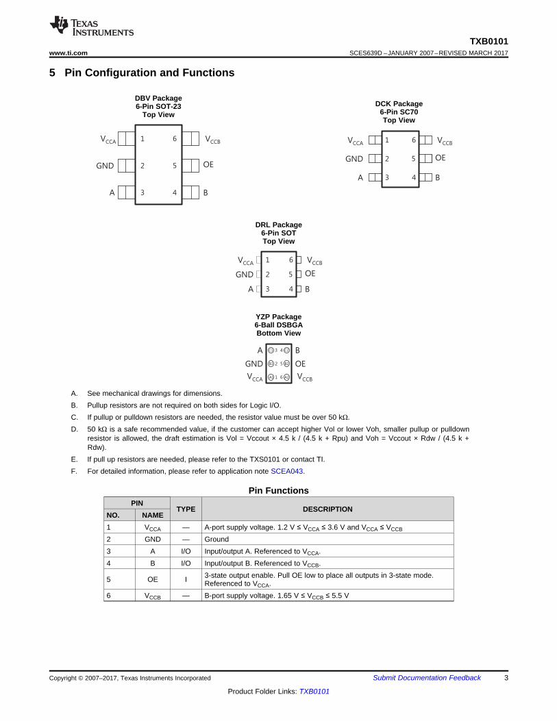
5 Pin Configuration and Functions
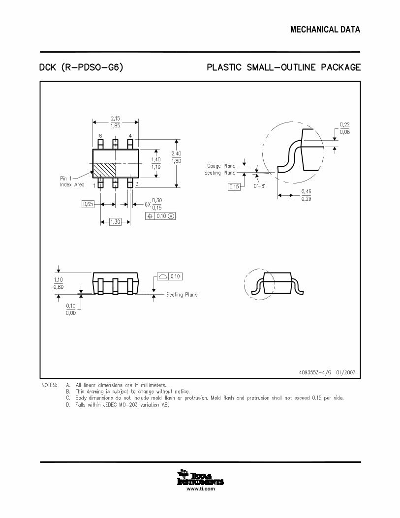
DBV Package6-Pin SOT-23
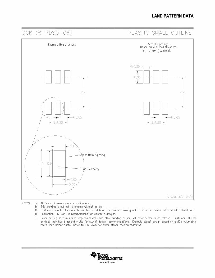
Top ViewDCK Package
6-Pin SC70Top View
DRL Package6-Pin SOTTop View
YZP Package6-Ball DSBGABottom View
A. See mechanical drawings for dimensions.B. Pullup resistors are not required on both sides for Logic I/O.C. If pullup or pulldown resistors are needed, the resistor value must be over 50 kΩ.D. 50 kΩ is a safe recommended value, if the customer can accept higher Vol or lower Voh, smaller pullup or pulldown
resistor is allowed, the draft estimation is Vol = Vccout × 4.5 k / (4.5 k + Rpu) and Voh = Vccout × Rdw / (4.5 k +Rdw).
E. If pull up resistors are needed, please refer to the TXS0101 or contact TI.F. For detailed information, please refer to application note SCEA043.
Pin FunctionsPIN
TYPE DESCRIPTIONNO. NAME1 VCCA — A-port supply voltage. 1.2 V ≤ VCCA ≤ 3.6 V and VCCA ≤ VCCB
2 GND — Ground3 A I/O Input/output A. Referenced to VCCA.4 B I/O Input/output B. Referenced to VCCB.
5 OE I 3-state output enable. Pull OE low to place all outputs in 3-state mode.Referenced to VCCA.
6 VCCB — B-port supply voltage. 1.65 V ≤ VCCB ≤ 5.5 V

4
TXB0101SCES639D –JANUARY 2007–REVISED MARCH 2017 www.ti.com
Product Folder Links: TXB0101
Submit Documentation Feedback Copyright © 2007–2017, Texas Instruments Incorporated
(1) Stresses beyond those listed under Absolute Maximum Ratings may cause permanent damage to the device. These are stress ratingsonly, and functional operation of the device at these or any other conditions beyond those indicated under Recommended OperatingConditions is not implied. Exposure to absolute-maximum-rated conditions for extended periods may affect device reliability.
(2) The input and output negative Voltage ratings may be exceeded if the input and output current ratings are observed.(3) The value of VCCA and VCCB are provided in the recommended operating conditions table.
6 Specification
6.1 Absolute Maximum Ratingsover operating free-air temperature range (unless otherwise noted) (1)
MIN MAX UNITVCCA Supply voltage –0.5 4.6
VVCCB Supply voltage –0.5 6.5VI Input voltage (2) –0.5 6.5 VVO Voltage applied to any output in the high-impedance or power-off state (2) –0.5 6.5 V
VO Voltage applied to any output in the high or low state (2) (3) A port –0.5 VCCA + 0.5V
B port –0.5 VCCB + 0.5IIK Input clamp current VI < 0 –50 mAIOK Output clamp current VO < 0 –50 mAIO Continuous output current ±50 mA
Continuous current through VCCA, VCCB, or GND ±100 mATJMAX Absolute maximum junction temperature 150 °CTstg Storage temperature –65 150 °C
(1) JEDEC document JEP155 states that 500 V HBM allows safe manufacturing with a standard ESD control process.(2) JEDEC document JEP157 states that 250 V CDM allows safe manufacturing with a standard ESD control process.
6.2 ESD RatingsVALUE UNIT
TXB0101 Port A
V(ESD) Electrostatic dischargeHuman body model (HBM), per ANSI/ESDA/JEDEC JS-001 (1) ±2000
VCharged-device model (CDM), per JEDEC specification JESD22-C101 (2) ±1500
TXB0101 Port B
V(ESD) Electrostatic dischargeHuman body model (HBM), per ANSI/ESDA/JEDEC JS-001 (1) ±15 kVCharged-device model (CDM), per JEDEC specification JESD22-C101 (2) ±1500 V
(1) The A and B sides of an unused data I/O pair must be held in the same state, i.e., both at VCCI or both at GND.(2) VCCA must be less than or equal to VCCB and must not exceed 3.6 V.(3) VCCI is the supply voltage associated with the input port.
6.3 Recommended Operating ConditionsSee (1) (2).
VCCA VCCB MIN MAX UNITVCCA Supply voltage
1.2 3.6V
VCCB 1.65 5.5
VIH High-level input voltageData inputs 1.2 V to 3.6 V 1.65 V to 5.5 V VCCI × 0.65 (3) VCCI VOE 1.2 V to 3.6 V 1.65 V to 5.5 V VCCA × 0.65 5.5
VIL Low-level input voltageData inputs 1.2 V to 5.5 V 1.65 V to 5.5 V 0 VCCI × 0.35 (3)
VOE 1.2 V to 3.6 V 1.65 V to 5.5 V 0 VCCA × 0.35
Δt/Δv Input transitionrise or fall rate
A-port inputs 1.2 V to 3.6 V 1.65 V to 5.5 V 40ns/V
B-port inputs 1.2 V to 3.6 V1.65 V to 3.6 V 404.5 V to 5.5 V 30
TA Operating free-air temperature –40 85 °C
5
TXB0101www.ti.com SCES639D –JANUARY 2007–REVISED MARCH 2017
Product Folder Links: TXB0101
Submit Documentation FeedbackCopyright © 2007–2017, Texas Instruments Incorporated
(1) For more information about traditional and new thermal metrics, see the Semiconductor and IC Package Thermal Metrics applicationreport.
6.4 Thermal Information
THERMAL METRIC (1)
TXB0101
UNITDBV (SOT-23)
DCK(SC70)
DRL (SOT) YZP(DSBGA)
6 PINS 6 PINS 6 PINS 6 PINSRθJA Junction-to-ambient thermal resistance 192.3 266.9 204.2 105.8 °C/WRθJC(top) Junction-to-case (top) thermal resistance 164.8 80.4 76.4 1.6 °C/WRθJB Junction-to-board thermal resistance 38.6 99.1 38.7 10.8 °C/WψJT Junction-to-top characterization parameter 43.7 1.5 3.4 3.1 °C/WψJB Junction-to-board characterization parameter 38.1 98.3 38.5 10.8 °C/WRθJC(bot) Junction-to-case (bottom) thermal resistance N/A N/A N/A N/A °C/W
(1) VCCI is the supply voltage associated with the input port.(2) VCCO is the supply voltage associated with the output port.
6.5 Electrical Characteristicsover recommended operating free-air temperature range (unless otherwise noted) (1) (2)
PARAMETER TESTCONDITIONS VCCA VCCB
TA = 25°C –40°C to 85°CUNIT
MIN TYP MAX MIN TYP MAX
VOHA IOH = –20 μA1.2 V 1.1
V1.4 V to 3.6 V VCCA – 0.4
VOLA IOL = 20 μA1.2 V 0.9
V1.4 V to 3.6 V 0.4
VOHB IOH = –20 μA 1.65 V to 5.5 V VCCB – 0.4 VVOLB IOL = 20 μA 1.65 V to 5.5 V 0.4 VII OE 1.2 V to 3.6 V 1.65 V to 5.5 V ±1 ±2 μA
IoffA port 0 V 0 V to 5.5 V ±1 ±2
μAB port 0 V to 3.6 V 0 V ±1 ±2
IOZ A or B port OE = GND 1.2 V to 3.6 V 1.65 V to 5.5 V ±1 ±2 μA
ICCAVI = VCCI or GND,IO = 0
1.2 V 1.65 V to 5.5 V 0.06
μA1.4 V to 3.6 V 1.65 V to 5.5 V 3
3.6 V 0 V 20 V 5.5 V –2
ICCBVI = VCCI or GND,IO = 0
1.2 V 1.65 V to 5.5 V 3.4
μA1.4 V to 3.6 V 1.65 V to 5.5 V 5
3.6 V 0 V –20 V 5.5 V 2
ICCA + ICCBVI = VCCI or GND,IO = 0
1.2 V 1.65 V to 5.5 V 3.5μA
1.4 V to 3.6 V 1.65 V to 5.5 V 8
ICCZA
VI = VCCI or GND,IO = 0,OE = GND
1.2 V 1.65 V to 5.5 V 0.05μA
1.4 V to 3.6 V 1.65 V to 5.5 V 3
ICCZB
VI = VCCI or GND,IO = 0,OE = GND
1.2 V 1.65 V to 5.5 V 3.3μA
1.4 V to 3.6 V 1.65 V to 5.5 V 5
Ci OE 1.2 V to 3.6 V 1.65 V to 5.5 V 2.5 3 pF
CioA port
1.2 V to 3.6 V 1.65 V to 5.5 V5 6
pFB port 11 13
6
TXB0101SCES639D –JANUARY 2007–REVISED MARCH 2017 www.ti.com
Product Folder Links: TXB0101
Submit Documentation Feedback Copyright © 2007–2017, Texas Instruments Incorporated
6.6 Timing Requirements, VCCA = 1.2 VTA = 25°C, VCCA = 1.2 V
VCCB = 1.8 V VCCB = 2.5 V VCCB = 3.3 V VCCB = 5 VUNIT
TYP TYP TYP TYPData rate 20 20 20 20 Mbps
tw Pulse duration Data inputs 50 50 50 50 ns
6.7 Timing Requirements, VCCA = 1.5 V ± 0.1 Vover recommended operating free-air temperature range, VCCA = 1.5 V ± 0.1 V (unless otherwise noted)
VCCB = 1.8 V± 0.15 V
VCCB = 2.5 V± 0.2 V
VCCB = 3.3 V± 0.3 V
VCCB = 5 V± 0.5 V UNIT
MIN MAX MIN MAX MIN MAX MIN MAXData rate 40 40 40 40 Mbps
tw Pulse duration Data inputs 25 25 25 25 ns
6.8 Timing Requirements, VCCA = 1.8 V ± 0.15 Vover recommended operating free-air temperature range, VCCA = 1.8 V ± 0.15 V (unless otherwise noted)
VCCB = 1.8 V± 0.15 V
VCCB = 2.5 V± 0.2 V
VCCB = 3.3 V± 0.3 V
VCCB = 5 V± 0.5 V UNIT
MIN MAX MIN MAX MIN MAX MIN MAXData rate 60 60 60 60 Mbps
tw Pulse duration Data inputs 17 17 17 17 ns
6.9 Timing Requirements, VCCA = 2.5 V ± 0.2 Vover recommended operating free-air temperature range, VCCA = 2.5 V ± 0.2 V (unless otherwise noted)
VCCB = 2.5 V± 0.2 V
VCCB = 3.3 V± 0.3 V
VCCB = 5 V± 0.5 V UNIT
MIN MAX MIN MAX MIN MAXData rate 100 100 100 Mbps
tw Pulse duration Data inputs 10 10 10 ns
6.10 Timing Requirements, VCCA = 3.3 V ± 0.3 Vover recommended operating free-air temperature range, VCCA = 3.3 V ± 0.3 V (unless otherwise noted)
VCCB = 3.3 V± 0.3 V
VCCB = 5 V± 0.5 V UNIT
MIN MAX MIN MAXData rate 100 100 Mbps
tw Pulse duration Data inputs 10 10 ns

7
TXB0101www.ti.com SCES639D –JANUARY 2007–REVISED MARCH 2017
Product Folder Links: TXB0101
Submit Documentation FeedbackCopyright © 2007–2017, Texas Instruments Incorporated
6.11 Switching Characteristics, VCCA = 1.2 VTA = 25°C, VCCA = 1.2 V
PARAMETER FROM(INPUT)
TO(OUTPUT)
VCCB = 1.8 V VCCB = 2.5 V VCCB = 3.3 V VCCB = 5 VUNIT
TYP TYP TYP TYP
tpdA B 6.9 5.7 5.3 5.5
nsB A 7.4 6.4 6 5.8
ten OEA 1 1 1 1
μsB 1 1 1 1
tdis OEA 18 15 14 14
nsB 20 17 16 16
trA, tfA A-port rise and fall times 4.2 4.2 4.2 4.2 nstrB, tfB B-port rise and fall times 2.1 1.5 1.2 1.1 nsMax data rate 20 20 20 20 Mbps
6.12 Switching Characteristics, VCCA = 1.5 V ± 0.1 Vover recommended operating free-air temperature range, VCCA = 1.5 V ± 0.1 V (unless otherwise noted)
PARAMETER FROM(INPUT)
TO(OUTPUT)
VCCB = 1.8 V± 0.15 V
VCCB = 2.5 V± 0.2 V
VCCB = 3.3 V± 0.3 V
VCCB = 5 V± 0.5 V UNIT
MIN MAX MIN MAX MIN MAX MIN MAX
tpdA B 1.4 12.9 1.2 10.1 1.1 10 0.8 9.9
nsB A 0.9 14.2 0.7 12 0.4 11.7 0.3 13.7
ten OEA 1 1 1 1
μsB 1 1 1 1
tdis OEA 5.9 31 5.7 25.9 5.6 23 5.7 22.4
nsB 5.4 30.3 4.9 22.8 4.8 20 4.9 19.5
trA, tfA A-port rise and fall times 1.4 5.1 1.4 5.1 1.4 5.1 1.4 5.1 nstrB, tfB B-port rise and fall times 0.9 4.5 0.6 3.2 0.5 2.8 0.4 2.7 nsMax data rate 40 40 40 40 Mbps
6.13 Switching Characteristics, VCCA = 1.8 V ± 0.15 Vover recommended operating free-air temperature range, VCCA = 1.8 V ± 0.15 V (unless otherwise noted)
PARAMETER FROM(INPUT)
TO(OUTPUT)
VCCB = 1.8 V± 0.15 V
VCCB = 2.5 V± 0.2 V
VCCB = 3.3 V± 0.3 V
VCCB = 5 V± 0.5 V UNIT
MIN MAX MIN MAX MIN MAX MIN MAX
tpdA B 1.6 11 1.4 7.7 1.3 6.8 1.2 6.5
nsB A 1.5 12 1.3 8.4 1 7.6 0.9 7.1
ten OEA 1 1 1 1
μsB 1 1 1 1
tdis OEA 5.9 31 5.1 21.3 5 19.3 5 17.4
nsB 5.4 30.3 4.4 20.8 4.2 17.9 4.3 16.3
trA, tfA A-port rise and fall times 1 4.2 1.1 4.1 1.1 4.1 1.1 4.1 nstrB, tfB B-port rise and fall times 0.9 4.5 0.6 3.2 0.5 2.8 0.4 2.7 nsMax data rate 60 60 60 60 Mbps
8
TXB0101SCES639D –JANUARY 2007–REVISED MARCH 2017 www.ti.com
Product Folder Links: TXB0101
Submit Documentation Feedback Copyright © 2007–2017, Texas Instruments Incorporated
6.14 Switching Characteristics, VCCA = 2.5 V ± 0.2 Vover recommended operating free-air temperature range, VCCA = 2.5 V ± 0.2 V (unless otherwise noted)
PARAMETER FROM(INPUT)
TO(OUTPUT)
VCCB = 2.5 V± 0.2 V
VCCB = 3.3 V± 0.3 V
VCCB = 5 V± 0.5 V UNIT
MIN MAX MIN MAX MIN MAX
tpdA B 1.1 6.3 1 5.2 0.9 4.7
nsB A 1.2 6.6 1.1 5.1 0.9 4.4
ten OEA 1 1 1
μsB 1 1 1
tdis OEA 5.1 21.3 4.6 15.2 4.6 13.2
nsB 4.4 20.8 3.8 16 3.9 13.9
trA, tfA A-port rise and fall times 0.8 3 0.8 3 0.8 3 nstrB, tfB B-port rise and fall times 0.7 3 0.5 2.8 0.4 2.7 nsMax data rate 100 100 100 Mbps
6.15 Switching Characteristics, VCCA = 3.3 V ± 0.3 Vover recommended operating free-air temperature range, VCCA = 3.3 V ± 0.3 V (unless otherwise noted)
PARAMETER FROM(INPUT)
TO(OUTPUT)
VCCB = 3.3 V± 0.3 V
VCCB = 5 V± 0.5 V UNIT
MIN MAX MIN MAX
tpdA B 0.9 4.7 0.8 4
nsB A 1 4.9 0.9 4.5
ten OEA 1 1
μsB 1 1
tdis OEA 4.6 15.2 4.3 12.1
nsB 3.8 16 3.4 13.2
trA, tfA A-port rise and fall times 0.7 2.5 0.7 2.5 nstrB, tfB B-port rise and fall times 0.5 2.3 0.4 2.7 nsMax data rate 100 100 Mbps
6.16 Operating CharacteristicsTA = 25°C
PARAMETER TEST CONDITIONS
VCCA
UNIT
1.2 V 1.2 V 1.5 V 1.8 V 2.5 V 2.5 V 3.3 VVCCB
5 V 1.8 V 1.8 V 1.8 V 2.5 V 5 V3.3 V
to5 V
TYP TYP TYP TYP TYP TYP TYP
CpdAA-port input, B-port output
CL = 0, f = 10 MHz,tr = tf = 1 ns,OE = VCCA
(outputs enabled)
7.8 8 8 7 7 8 8
pFB-port input, A-port output 12 11 11 11 11 11 11
CpdBA-port input, B-port output 38.1 28 29 29 29 29 30B-port input, A-port output 25.4 18 17 17 18 20 21
CpdAA-port input, B-port output
CL = 0, f = 10 MHz,tr = tf = 1 ns,OE = GND
(outputs disabled)
0.01 0.01 0.01 0.01 0.01 0.01 0.01
pFB-port input, A-port output 0.01 0.01 0.01 0.01 0.01 0.01 0.01
CpdBA-port input, B-port output 0.01 0.01 0.01 0.01 0.01 0.01 0.02B-port input, A-port output 0.01 0.01 0.01 0.01 0.01 0.01 0.03

VCCB (V)
B P
ort
I/O
Capacita
nce (
pF
)
0 0.5 1 1.5 2 2.5 3 3.5 4 4.5 5 5.50
2
4
6
8
10
12
D003
25°C (Room Temp)-40°C85°C
VCCA (V)
OE
Pin
Inp
ut
Ca
pa
citan
ce
(p
F)
0 0.5 1 1.5 2 2.5 3 3.5 40
1
2
3
4
5
6
D001
25°C (Room Temp)-40°C85°C
VCCA (V)
AP
ort
I/O
Ca
pa
cita
nce
(p
F)
0 0.5 1 1.5 2 2.5 3 3.5 40
1
2
3
4
5
6
D002
25°C (Room Temp)-40°C85°C
9
TXB0101www.ti.com SCES639D –JANUARY 2007–REVISED MARCH 2017
Product Folder Links: TXB0101
Submit Documentation FeedbackCopyright © 2007–2017, Texas Instruments Incorporated
6.17 Typical Characteristics
VCCB = 3.3 V
Figure 1. Input Capacitance for OE pin (CI) vs Power Supply(VCCA)
VCCB = 3.3 V
Figure 2. Capacitance for A Port I/O Pins (CiO) vs PowerSupply (VCCA)
VCCA = 1.8 V
Figure 3. Capacitance for B Port I/O Pins (CiO) vs Power Supply (VCCB)
From Output
Under Test
LOAD CIRCUIT FOR
ENABLE/DISABLE
TIME MEASUREMENT
S1
2 × VCCO
Open
50 kΩ
VCCI
0 V
VCCI/2 VCCI/2
tw
VOLTAGE WAVEFORMS
PROPAGATION DELAY TIMES
VOLTAGE WAVEFORMS
PULSE DURATION
Input
tPZL/tPLZ
tPHZ/tPZH
2 × VCCO
Open
TEST S1
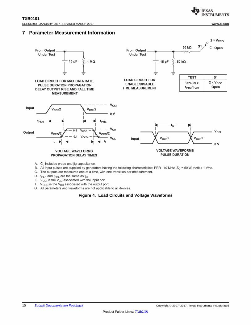
A. CL includes probe and jig capacitance.
B. All input pulses are supplied by generators having the following characteristics: PRR 10 MHz, ZO = 50 W, dv/dt ≥ 1 V/ns.
C. The outputs are measured one at a time, with one transition per measurement.
D. tPLH and tPHL are the same as tpd.
E. VCCI is the VCC associated with the input port.
F. VCCO is the VCC associated with the output port.
G. All parameters and waveforms are not applicable to all devices.
50 kΩFrom Output
Under Test
1 MΩ15 pF 15 pF
LOAD CIRCUIT FOR MAX DATA RATE,
PULSE DURATION PROPAGATION
DELAY OUTPUT RISE AND FALL TIME
MEASUREMENT
tPLH tPHL
0 V
VCCO/2
VCCI/2 VCCI/2
0.9 VCCOVCCO/2
tr
0.1 VCCO
tf
VCCIInput
OutputVOH
VOL
10
TXB0101SCES639D –JANUARY 2007–REVISED MARCH 2017 www.ti.com
Product Folder Links: TXB0101
Submit Documentation Feedback Copyright © 2007–2017, Texas Instruments Incorporated
7 Parameter Measurement Information
Figure 4. Load Circuits and Voltage Waveforms
OE
A
VCCA VCCB
One-Shot
4 N
One-Shot
4 N
B
11
TXB0101www.ti.com SCES639D –JANUARY 2007–REVISED MARCH 2017
Product Folder Links: TXB0101
Submit Documentation FeedbackCopyright © 2007–2017, Texas Instruments Incorporated
8 Detailed Description
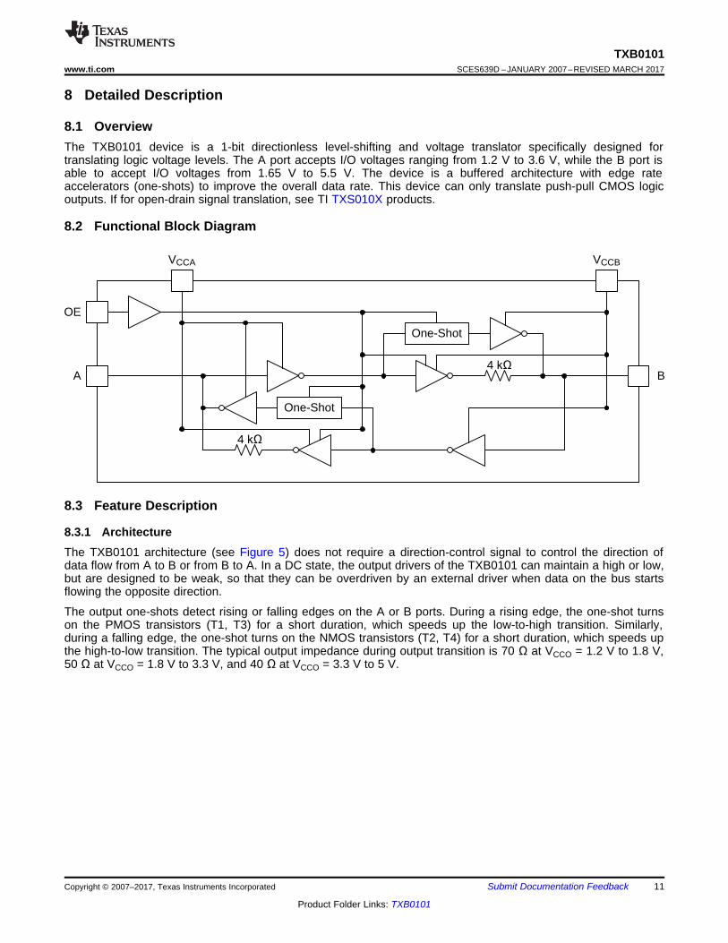
8.1 OverviewThe TXB0101 device is a 1-bit directionless level-shifting and voltage translator specifically designed fortranslating logic voltage levels. The A port accepts I/O voltages ranging from 1.2 V to 3.6 V, while the B port isable to accept I/O voltages from 1.65 V to 5.5 V. The device is a buffered architecture with edge rateaccelerators (one-shots) to improve the overall data rate. This device can only translate push-pull CMOS logicoutputs. If for open-drain signal translation, see TI TXS010X products.
8.2 Functional Block Diagram
8.3 Feature Description
8.3.1 ArchitectureThe TXB0101 architecture (see Figure 5) does not require a direction-control signal to control the direction ofdata flow from A to B or from B to A. In a DC state, the output drivers of the TXB0101 can maintain a high or low,but are designed to be weak, so that they can be overdriven by an external driver when data on the bus startsflowing the opposite direction.
The output one-shots detect rising or falling edges on the A or B ports. During a rising edge, the one-shot turnson the PMOS transistors (T1, T3) for a short duration, which speeds up the low-to-high transition. Similarly,during a falling edge, the one-shot turns on the NMOS transistors (T2, T4) for a short duration, which speeds upthe high-to-low transition. The typical output impedance during output transition is 70 Ω at VCCO = 1.2 V to 1.8 V,50 Ω at VCCO = 1.8 V to 3.3 V, and 40 Ω at VCCO = 3.3 V to 5 V.

4k
4k
A B
VCCA VCCB
One
Shot
One
Shot
One
Shot
One
Shot
T1
T2
T3
T4
12
TXB0101SCES639D –JANUARY 2007–REVISED MARCH 2017 www.ti.com
Product Folder Links: TXB0101
Submit Documentation Feedback Copyright © 2007–2017, Texas Instruments Incorporated
Feature Description (continued)
Figure 5. Architecture of TXB0101 I/O Cell
8.3.2 Power UpDuring operation, ensure that VCCA ≤ VCCB at all times. During power up sequencing, VCCA ≥ VCCB does notdamage the device, so any power supply can be ramped up first. The TXB0101 has circuitry that disables alloutput ports when either VCC is switched off (VCCA/B = 0 V) and are placed in high-impedance state.
8.3.3 Enable and DisableThe TXB0101 has an OE input that is used to disable the device by setting OE = low, which places all I/Os in thehigh-impedance (Hi-Z) state. The disable time (tdis) indicates the delay between when OE goes low and when theoutputs are actually disabled (Hi-Z). The enable time (ten) indicates the amount of time the user must allow forthe one-shot circuitry to become operational after OE is taken high.
8.3.4 Pullup or Pulldown Resistors on I/O LinesThe TXB0101 is designed to drive capacitive loads of up to 70 pF. The output drivers of the TXB0101 have low-DC drive strength. If pullup or pulldown resistors are connected externally to the data I/Os, their values must bekept higher than 50 kΩ to ensure that they do not contend with the output drivers of the TXB0101.
For the same reason, the TXB0101 should not be used in applications such as I2C or 1-Wire where an open-drain driver is connected on the bidirectional data I/O. For these applications, use a device from the TI TXS010Xseries of level translators.
8.4 Device Functional ModesThe TXB0101 device has two functional modes, enabled and disabled. To disable the device set the OE inputlow, which places all I/Os in a high-impedance state. Setting the OE input high will enable the device.
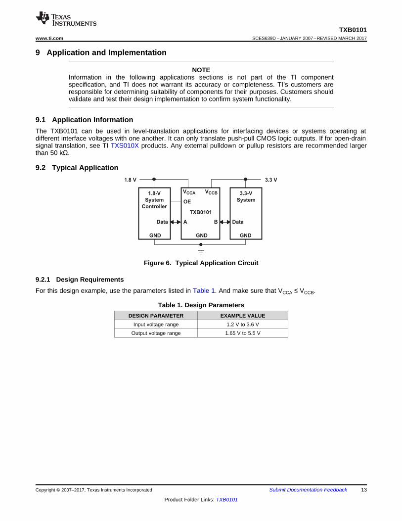
Data
GNDGNDGND
Data A B
VCCA VCCB
OE
1.8-V
System
Controller
3.3-V
System
1.8 V 3.3 V
TXB0101
13
TXB0101www.ti.com SCES639D –JANUARY 2007–REVISED MARCH 2017
Product Folder Links: TXB0101
Submit Documentation FeedbackCopyright © 2007–2017, Texas Instruments Incorporated
9 Application and Implementation
NOTEInformation in the following applications sections is not part of the TI componentspecification, and TI does not warrant its accuracy or completeness. TI’s customers areresponsible for determining suitability of components for their purposes. Customers shouldvalidate and test their design implementation to confirm system functionality.
9.1 Application InformationThe TXB0101 can be used in level-translation applications for interfacing devices or systems operating atdifferent interface voltages with one another. It can only translate push-pull CMOS logic outputs. If for open-drainsignal translation, see TI TXS010X products. Any external pulldown or pullup resistors are recommended largerthan 50 kΩ.
9.2 Typical Application
Figure 6. Typical Application Circuit
9.2.1 Design RequirementsFor this design example, use the parameters listed in Table 1. And make sure that VCCA ≤ VCCB.
Table 1. Design ParametersDESIGN PARAMETER EXAMPLE VALUE
Input voltage range 1.2 V to 3.6 VOutput voltage range 1.65 V to 5.5 V
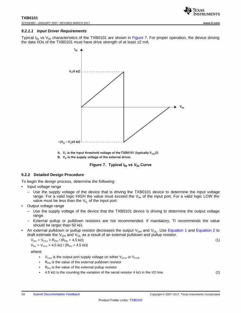
A. V is the input threshold voltage of the TXB0101 (typically /2.
B.T V
V is the supply voltage of the external driver.CCI
D
–(V – V )/4 kD T Ω
V /4 kT Ω
VIN
IIN
14
TXB0101SCES639D –JANUARY 2007–REVISED MARCH 2017 www.ti.com
Product Folder Links: TXB0101
Submit Documentation Feedback Copyright © 2007–2017, Texas Instruments Incorporated
9.2.1.1 Input Driver RequirementsTypical IIN vs VIN characteristics of the TXB0101 are shown in Figure 7. For proper operation, the device drivingthe data I/Os of the TXB0101 must have drive strength of at least ±2 mA.
Figure 7. Typical IIN vs VIN Curve
9.2.2 Detailed Design ProcedureTo begin the design process, determine the following:• Input voltage range
– Use the supply voltage of the device that is driving the TXB0101 device to determine the input voltagerange. For a valid logic HIGH the value must exceed the VIH of the input port. For a valid logic LOW thevalue must be less than the VIL of the input port.
• Output voltage range– Use the supply voltage of the device that the TXB0101 device is driving to determine the output voltage
range.– External pullup or pulldown resistors are not recommended. If mandatory, TI recommends the value
should be larger than 50 kΩ.• An external pulldown or pullup resistor decreases the output VOH and VOL. Use Equation 1 and Equation 2 to
draft estimate the VOH and VOL as a result of an external pulldown and pullup resistor.VOH = VCCx × RPD / (RPD + 4.5 kΩ) (1)VOL = VCCx × 4.5 kΩ / (RPU + 4.5 kΩ)
where• VCCx is the output port supply voltage on either VCCA or VCCB
• RPD is the value of the external pulldown resistor• RPU is the value of the external pullup resistor• 4.5 kΩ is the counting the variation of the serial resistor 4 kΩ in the I/O line. (2)
200 ns/div
2V
/div
15
TXB0101www.ti.com SCES639D –JANUARY 2007–REVISED MARCH 2017
Product Folder Links: TXB0101
Submit Documentation FeedbackCopyright © 2007–2017, Texas Instruments Incorporated
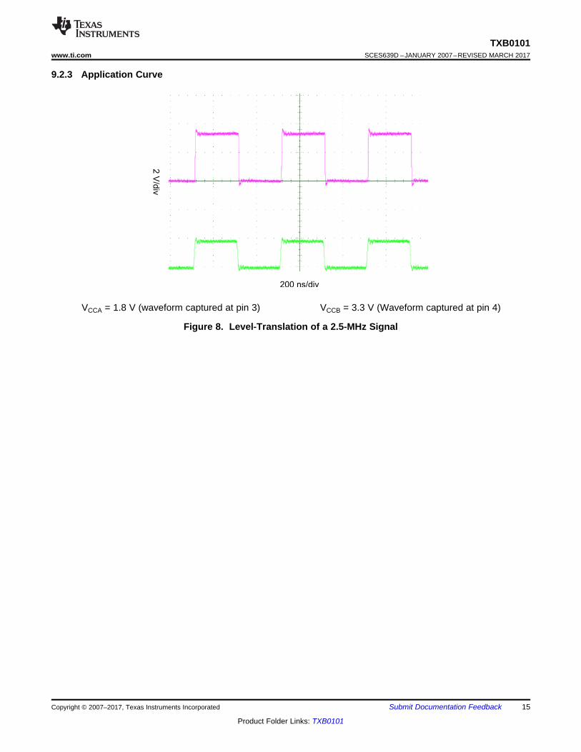
9.2.3 Application Curve
VCCA = 1.8 V (waveform captured at pin 3) VCCB = 3.3 V (Waveform captured at pin 4)
Figure 8. Level-Translation of a 2.5-MHz Signal
GND
B
VCCB
LEGEND
VIA to Power Plane
VIA to GND Plane (Inner Layer)
Polygonal Copper Pour
VCCA1
2
3 A
Keep OE low until VCCA and VCCB
are powered up
6
5
4
Bypass CapacitorBypass Capacitor
OETXB0101
VC
CA
To/From Controller/System
To/From
Controller/System
16
TXB0101SCES639D –JANUARY 2007–REVISED MARCH 2017 www.ti.com
Product Folder Links: TXB0101
Submit Documentation Feedback Copyright © 2007–2017, Texas Instruments Incorporated
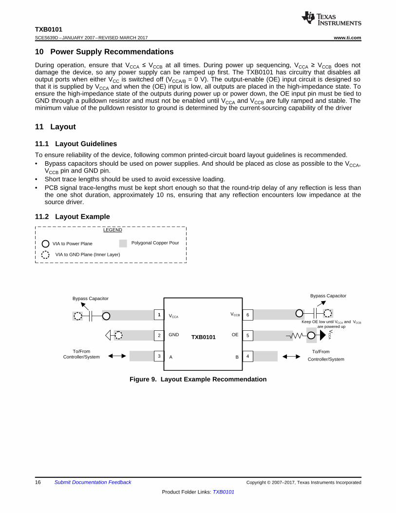
10 Power Supply RecommendationsDuring operation, ensure that VCCA ≤ VCCB at all times. During power up sequencing, VCCA ≥ VCCB does notdamage the device, so any power supply can be ramped up first. The TXB0101 has circuitry that disables alloutput ports when either VCC is switched off (VCCA/B = 0 V). The output-enable (OE) input circuit is designed sothat it is supplied by VCCA and when the (OE) input is low, all outputs are placed in the high-impedance state. Toensure the high-impedance state of the outputs during power up or power down, the OE input pin must be tied toGND through a pulldown resistor and must not be enabled until VCCA and VCCB are fully ramped and stable. Theminimum value of the pulldown resistor to ground is determined by the current-sourcing capability of the driver
11 Layout
11.1 Layout GuidelinesTo ensure reliability of the device, following common printed-circuit board layout guidelines is recommended.• Bypass capacitors should be used on power supplies. And should be placed as close as possible to the VCCA,
VCCB pin and GND pin.• Short trace lengths should be used to avoid excessive loading.• PCB signal trace-lengths must be kept short enough so that the round-trip delay of any reflection is less than
the one shot duration, approximately 10 ns, ensuring that any reflection encounters low impedance at thesource driver.
11.2 Layout Example
Figure 9. Layout Example Recommendation

17
TXB0101www.ti.com SCES639D –JANUARY 2007–REVISED MARCH 2017
Product Folder Links: TXB0101
Submit Documentation FeedbackCopyright © 2007–2017, Texas Instruments Incorporated
12 Device and Documentation Support
12.1 Receiving Notification of Documentation UpdatesTo receive notification of documentation updates, navigate to the device product folder on ti.com. In the upperright corner, click on Alert me to register and receive a weekly digest of any product information that haschanged. For change details, review the revision history included in any revised document.
12.2 Community ResourcesThe following links connect to TI community resources. Linked contents are provided "AS IS" by the respectivecontributors. They do not constitute TI specifications and do not necessarily reflect TI's views; see TI's Terms ofUse.
TI E2E™ Online Community TI's Engineer-to-Engineer (E2E) Community. Created to foster collaborationamong engineers. At e2e.ti.com, you can ask questions, share knowledge, explore ideas and helpsolve problems with fellow engineers.
Design Support TI's Design Support Quickly find helpful E2E forums along with design support tools andcontact information for technical support.
12.3 TrademarksNanoFree, E2E are trademarks of Texas Instruments.All other trademarks are the property of their respective owners.
12.4 Electrostatic Discharge CautionThese devices have limited built-in ESD protection. The leads should be shorted together or the device placed in conductive foamduring storage or handling to prevent electrostatic damage to the MOS gates.
12.5 GlossarySLYZ022 — TI Glossary.
This glossary lists and explains terms, acronyms, and definitions.
13 Mechanical, Packaging, and Orderable InformationThe following pages include mechanical, packaging, and orderable information. This information is the mostcurrent data available for the designated devices. This data is subject to change without notice and revision ofthis document. For browser-based versions of this data sheet, refer to the left-hand navigation.

PACKAGE OPTION ADDENDUM
www.ti.com 17-Mar-2017
Addendum-Page 1
PACKAGING INFORMATION
Orderable Device Status(1)
Package Type PackageDrawing
Pins PackageQty
Eco Plan(2)
Lead/Ball Finish(6)
MSL Peak Temp(3)
Op Temp (°C) Device Marking(4/5)
Samples
TXB0101DBVR ACTIVE SOT-23 DBV 6 3000 Green (RoHS& no Sb/Br)
CU NIPDAU Level-1-260C-UNLIM -40 to 85 (NFCF ~ NFCR)
TXB0101DBVRG4 ACTIVE SOT-23 DBV 6 3000 Green (RoHS& no Sb/Br)
CU NIPDAU Level-1-260C-UNLIM -40 to 85 (NFCF ~ NFCR)
TXB0101DBVT ACTIVE SOT-23 DBV 6 250 Green (RoHS& no Sb/Br)
CU NIPDAU Level-1-260C-UNLIM -40 to 85 (NFCF ~ NFCR)
TXB0101DBVTG4 ACTIVE SOT-23 DBV 6 250 Green (RoHS& no Sb/Br)
CU NIPDAU Level-1-260C-UNLIM -40 to 85 (NFCF ~ NFCR)
TXB0101DCKR ACTIVE SC70 DCK 6 3000 Green (RoHS& no Sb/Br)
CU NIPDAU Level-1-260C-UNLIM -40 to 85 27O
TXB0101DCKRG4 ACTIVE SC70 DCK 6 3000 Green (RoHS& no Sb/Br)
CU NIPDAU Level-1-260C-UNLIM -40 to 85 27O
TXB0101DCKT ACTIVE SC70 DCK 6 250 Green (RoHS& no Sb/Br)
CU NIPDAU Level-1-260C-UNLIM 27O
TXB0101DCKTG4 ACTIVE SC70 DCK 6 250 Green (RoHS& no Sb/Br)
CU NIPDAU Level-1-260C-UNLIM -40 to 85 27O
TXB0101DRLR ACTIVE SOT-OTHER DRL 6 4000 Green (RoHS& no Sb/Br)
CU NIPDAU Level-1-260C-UNLIM -40 to 85 27R
TXB0101DRLT ACTIVE SOT-OTHER DRL 6 250 Green (RoHS& no Sb/Br)
CU NIPDAU Level-1-260C-UNLIM -40 to 85 27R
TXB0101YZPR ACTIVE DSBGA YZP 6 3000 Green (RoHS& no Sb/Br)
SNAGCU Level-1-260C-UNLIM -40 to 85 (277 ~ 27N)
(1) The marketing status values are defined as follows:ACTIVE: Product device recommended for new designs.LIFEBUY: TI has announced that the device will be discontinued, and a lifetime-buy period is in effect.NRND: Not recommended for new designs. Device is in production to support existing customers, but TI does not recommend using this part in a new design.PREVIEW: Device has been announced but is not in production. Samples may or may not be available.OBSOLETE: TI has discontinued the production of the device.
(2) Eco Plan - The planned eco-friendly classification: Pb-Free (RoHS), Pb-Free (RoHS Exempt), or Green (RoHS & no Sb/Br) - please check http://www.ti.com/productcontent for the latest availabilityinformation and additional product content details.TBD: The Pb-Free/Green conversion plan has not been defined.Pb-Free (RoHS): TI's terms "Lead-Free" or "Pb-Free" mean semiconductor products that are compatible with the current RoHS requirements for all 6 substances, including the requirement thatlead not exceed 0.1% by weight in homogeneous materials. Where designed to be soldered at high temperatures, TI Pb-Free products are suitable for use in specified lead-free processes.
PACKAGE OPTION ADDENDUM
www.ti.com 17-Mar-2017
Addendum-Page 2
Pb-Free (RoHS Exempt): This component has a RoHS exemption for either 1) lead-based flip-chip solder bumps used between the die and package, or 2) lead-based die adhesive used betweenthe die and leadframe. The component is otherwise considered Pb-Free (RoHS compatible) as defined above.Green (RoHS & no Sb/Br): TI defines "Green" to mean Pb-Free (RoHS compatible), and free of Bromine (Br) and Antimony (Sb) based flame retardants (Br or Sb do not exceed 0.1% by weightin homogeneous material)
(3) MSL, Peak Temp. - The Moisture Sensitivity Level rating according to the JEDEC industry standard classifications, and peak solder temperature.
(4) There may be additional marking, which relates to the logo, the lot trace code information, or the environmental category on the device.
(5) Multiple Device Markings will be inside parentheses. Only one Device Marking contained in parentheses and separated by a "~" will appear on a device. If a line is indented then it is a continuationof the previous line and the two combined represent the entire Device Marking for that device.
(6) Lead/Ball Finish - Orderable Devices may have multiple material finish options. Finish options are separated by a vertical ruled line. Lead/Ball Finish values may wrap to two lines if the finishvalue exceeds the maximum column width.
Important Information and Disclaimer:The information provided on this page represents TI's knowledge and belief as of the date that it is provided. TI bases its knowledge and belief on informationprovided by third parties, and makes no representation or warranty as to the accuracy of such information. Efforts are underway to better integrate information from third parties. TI has taken andcontinues to take reasonable steps to provide representative and accurate information but may not have conducted destructive testing or chemical analysis on incoming materials and chemicals.TI and TI suppliers consider certain information to be proprietary, and thus CAS numbers and other limited information may not be available for release.
In no event shall TI's liability arising out of such information exceed the total purchase price of the TI part(s) at issue in this document sold by TI to Customer on an annual basis.
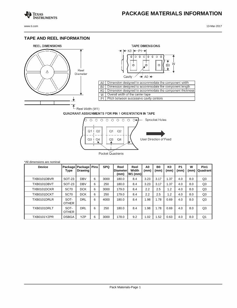
TAPE AND REEL INFORMATION
*All dimensions are nominal
Device PackageType
PackageDrawing
Pins SPQ ReelDiameter
(mm)
ReelWidth
W1 (mm)
A0(mm)
B0(mm)
K0(mm)
P1(mm)
W(mm)
Pin1Quadrant
TXB0101DBVR SOT-23 DBV 6 3000 180.0 8.4 3.23 3.17 1.37 4.0 8.0 Q3
TXB0101DBVT SOT-23 DBV 6 250 180.0 8.4 3.23 3.17 1.37 4.0 8.0 Q3
TXB0101DCKR SC70 DCK 6 3000 179.0 8.4 2.2 2.5 1.2 4.0 8.0 Q3
TXB0101DCKT SC70 DCK 6 250 179.0 8.4 2.2 2.5 1.2 4.0 8.0 Q3
TXB0101DRLR SOT-OTHER
DRL 6 4000 180.0 8.4 1.98 1.78 0.69 4.0 8.0 Q3
TXB0101DRLT SOT-OTHER
DRL 6 250 180.0 8.4 1.98 1.78 0.69 4.0 8.0 Q3
TXB0101YZPR DSBGA YZP 6 3000 178.0 9.2 1.02 1.52 0.63 4.0 8.0 Q1
PACKAGE MATERIALS INFORMATION
www.ti.com 13-Mar-2017
Pack Materials-Page 1
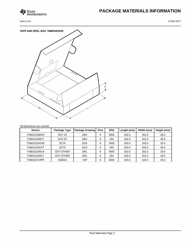
*All dimensions are nominal
Device Package Type Package Drawing Pins SPQ Length (mm) Width (mm) Height (mm)
TXB0101DBVR SOT-23 DBV 6 3000 202.0 201.0 28.0
TXB0101DBVT SOT-23 DBV 6 250 202.0 201.0 28.0
TXB0101DCKR SC70 DCK 6 3000 203.0 203.0 35.0
TXB0101DCKT SC70 DCK 6 250 203.0 203.0 35.0
TXB0101DRLR SOT-OTHER DRL 6 4000 202.0 201.0 28.0
TXB0101DRLT SOT-OTHER DRL 6 250 202.0 201.0 28.0
TXB0101YZPR DSBGA YZP 6 3000 220.0 220.0 35.0
PACKAGE MATERIALS INFORMATION
www.ti.com 13-Mar-2017
Pack Materials-Page 2

www.ti.com
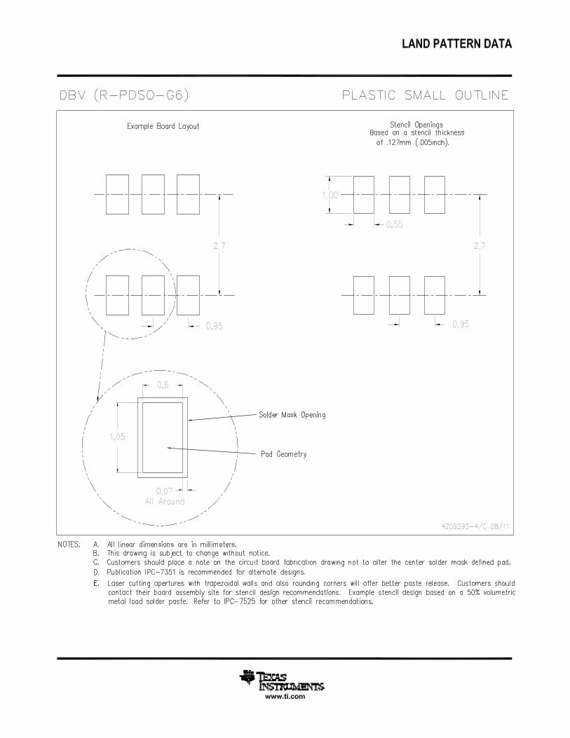
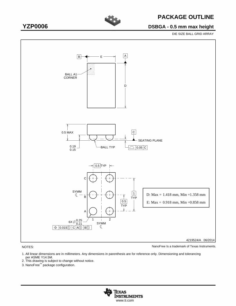
PACKAGE OUTLINE
C0.5 MAX
0.190.15
1TYP
0.5 TYP
6X 0.250.21
0.5TYP
B E A
D
4219524/A 06/2014
DSBGA - 0.5 mm max heightYZP0006DIE SIZE BALL GRID ARRAY
NOTES: 1. All linear dimensions are in millimeters. Any dimensions in parenthesis are for reference only. Dimensioning and tolerancing per ASME Y14.5M.2. This drawing is subject to change without notice.3. NanoFreeTM package configuration.
NanoFree Is a trademark of Texas Instruments.
BALL A1CORNER
SEATING PLANE
BALL TYP 0.05 C
B
A
1 2
0.015 C A B
SYMM
SYMM
C
SCALE 9.000
D: Max =
E: Max =
1.418 mm, Min =
0.918 mm, Min =
1.358 mm
0.858 mm

www.ti.com
EXAMPLE BOARD LAYOUT
6X ( )0.225(0.5) TYP
(0.5) TYP
( )METAL0.225 0.05 MAX
SOLDER MASKOPENING
METALUNDERMASK
( )SOLDER MASKOPENING
0.225
0.05 MIN
4219524/A 06/2014
DSBGA - 0.5 mm max heightYZP0006DIE SIZE BALL GRID ARRAY
NOTES: (continued) 4. Final dimensions may vary due to manufacturing tolerance considerations and also routing constraints. For more information, see Texas Instruments literature number SBVA017 (www.ti.com/lit/sbva017).
SYMM
SYMM
LAND PATTERN EXAMPLESCALE:40X
1 2
A
B
C
NON-SOLDER MASKDEFINED
(PREFERRED)
SOLDER MASK DETAILSNOT TO SCALE
SOLDER MASKDEFINED
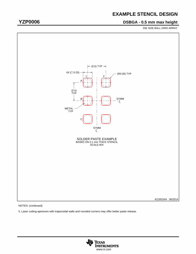
www.ti.com
EXAMPLE STENCIL DESIGN
(0.5)TYP
(0.5) TYP
6X ( 0.25) (R ) TYP0.05
METALTYP
4219524/A 06/2014
DSBGA - 0.5 mm max heightYZP0006DIE SIZE BALL GRID ARRAY
NOTES: (continued) 5. Laser cutting apertures with trapezoidal walls and rounded corners may offer better paste release.
SYMM
SYMM
SOLDER PASTE EXAMPLEBASED ON 0.1 mm THICK STENCIL
SCALE:40X
1 2
A
B
C